2.5a, dual-input, single-cell switchmode li-ion battery ... slusap4b –december 2011–revised...
TRANSCRIPT

SW
SYS
BAT
DRVPGND
PMIDU
USB
IUSB1
IUSB2
CE1
BOOT
HOST
PMIDI
IN
TEMP PACK+
+
PACK–
–
IUSB3
CE2PGCHG
VDPM
AC Adapter orWireless Power
SystemLoad
VBUS
D+
D–
GND
bq24165bq24166bq24167
www.ti.com SLUSAP4B –DECEMBER 2011–REVISED MARCH 2013
2.5A, Dual-Input, Single Cell Switch Mode Li-Ion Battery Charger with Power PathManagement
Check for Samples: bq24165 , bq24166, bq24167
1FEATURES APPLICATIONS• High-Efficiency Switch Mode Charger with • Handheld Products
Separate Power Path Control • Portable Media Players– Make a GSM Call with a Deeply Discharged • Portable Equipment
Battery or No Battery • Netbook and Portable Internet Devices– Instantly Startup System from a Deeply
Discharged Battery or No Battery DESCRIPTION• Dual Input Charger The bq24165, bq24166 and bq24167 are highly
integrated single cell Li-Ion battery charger and– 20V Input Rating, With Over-Voltagesystem power path management devices targeted forProtection (OVP)space-limited, portable applications with high capacity
– 6.5V for USB Input batteries. The single cell charger has dual inputs– 10.5V for IN Input which allow operation from either a USB port or
higher power input supply (i.e., AC adapter or– Integrated FETs for Up to 2.5A Charge Ratewireless charging input) for a versatile solution. The– Up to 2.5A from IN Input two inputs are fully isolated from each other and are
– Up to 1.5A from USB Input managed by the bq24165/166/167 with the IN inputhaving precedence.• Highly Integrated Battery N-Channel MOSFET
Controller for Power Path ManagementAPPLICATION SCHEMATIC• Safe and Accurate Battery Management
Functions– 0.5% Battery Regulation Accuracy– 10% Charge Current Accuracy
• Adjustable Charge Current, Input CurrentLimit, and VINDPM Threshold (for IN input)
• Easy JEITA Implementation– Charge Parameter Selector Inputs (CE1,
CE2) for (bq24165)• Voltage-based, NTC Monitoring Input (TS)
– Standard Temperature Range (bq24166)– JEITA Compatible (bq24167)
• Thermal Regulation Protection for OutputCurrent Control
• Low Battery Leakage Current, BAT Short-Circuit Protection
• Soft-Start Feature to Reduce Inrush Current• Thermal Shutdown and Protection• Available in Small 2.8mm x 2.8mm 49-ball
WCSP or 4mm x 4mm QFN-24 Packages
1
Please be aware that an important notice concerning availability, standard warranty, and use in critical applications ofTexas Instruments semiconductor products and disclaimers thereto appears at the end of this data sheet.
PRODUCTION DATA information is current as of publication date. Copyright © 2011–2013, Texas Instruments IncorporatedProducts conform to specifications per the terms of the TexasInstruments standard warranty. Production processing does notnecessarily include testing of all parameters.
bq24167 Not Recommended For New Designs
bq24165bq24166bq24167SLUSAP4B –DECEMBER 2011–REVISED MARCH 2013 www.ti.com
These devices have limited built-in ESD protection. The leads should be shorted together or the device placed in conductive foamduring storage or handling to prevent electrostatic damage to the MOS gates.
DESCRIPTION (CONTINUED)The power path management feature allows the bq24165/166/167 to power the system from a high efficiency DCto DC converter while simultaneously and independently charging the battery. The charger monitors the batterycurrent at all times and reduces the charge current when the system load requires current above the inputcurrent limit. This allows for proper charge termination and timer operation. The system voltage is regulated tothe battery voltage but will not drop below 3.5V. This minimum system voltage support enables the system to runwith a defective or absent battery pack and enables instant system turn-on even with a totally discharged batteryor no battery. The power-path management architecture also permits the battery to supplement the systemcurrent requirements when the adapter cannot deliver the peak system currents. This enables the use of asmaller adapter. The 2.5A input current capability allows for GSM phone calls as soon as the adapter is pluggedin regardless of the battery voltage.
The battery is charged in three phases: conditioning, constant current and constant voltage. In all charge phases,an internal control loop monitors the IC junction temperature and reduces the charge current if the internaltemperature threshold is exceeded. Additionally, the bq24166 and bq24167 offer a voltage-based battery packthermistor monitoring input (TS) that monitors battery temperature for safe charging. The TS function forbq24166 is JEITA compatible.
ORDERING INFORMATIONPART NUMBER USB OVP IN OVP NTC MONITORING (TS) JEITA COMPATIBLE Package
bq24165YFFR 6.5V 10.5 V No Yes WCSP
bq24165YFFT 6.5 V 10.5 V No Yes WCSP
bq24165RGER 6.5V 10.5 V No Yes QFN
bq24165RGET 6.5 V 10.5 V No Yes QFN
bq24166YFFR 6.5 V 10.5 V Yes No WCSP
bq24166YFFT 6.5 V 10.5 V Yes No WCSP
bq24166RGER 6.5 V 10.5 V Yes No QFN
bq24166RGET 6.5 V 10.5 V Yes No QFN
bq24167YFFR 6.5 V 10.5 V Yes Yes WCSP
bq24167YFFT 6.5 V 10.5 V Yes Yes WCSP
bq24167RGER 6.5 V 10.5 V Yes Yes QFN
bq24167RGET 6.5 V 10.5 V Yes Yes QFN
2 Submit Documentation Feedback Copyright © 2011–2013, Texas Instruments Incorporated
Product Folder Links: bq24165 bq24166 bq24167
bq24167 Not Recommended For New Designs

bq24165bq24166bq24167
www.ti.com SLUSAP4B –DECEMBER 2011–REVISED MARCH 2013
ABSOLUTE MAXIMUM RATINGS (1)
over operating free-air temperature range (unless otherwise noted)
VALUE/UNITS
Pin voltage range (with respect to PGND) IN, USB –2 V to 20 V
PMIDI, PMIDU, BOOT –0.3 V to 20 V
SW –0.7 V to 12V
ISET, ILIM, SCL, SYS, BAT, BGATE, DRV, PG, CHG, VDPM, IUSB_, –0.3 V to 7 VCE_,TS
BOOT to SW –0.3 V to 7 V
Output current (Continuous) SW 4.5 A
SYS, BAT 3.5 A
Input current (Continuous) IN 2.75 A
USB 1.75 A
Output sink current PG, CHG 10 mA
Operating free-air temperature range –40°C to 85°C
Junction temperature, TJ –40°C to 125°C
Storage temperature, TSTG –65°C to 150°C
Lead temperature (soldering, 10 s) 300°C
(1) Stresses beyond those listed under absolute maximum ratings may cause permanent damage to the device. These are stress ratingsonly, and functional operation of the device at these or any other conditions beyond those indicated under recommended operatingconditions is not implied. Exposure to absolute-maximum-rated conditions for extended periods may affect device reliability. All voltagevalues are with respect to the network ground terminal unless otherwise noted.
THERMAL INFORMATIONbq2416x
THERMAL METRIC (1) UNITS49 PINS (YFF) 24 PINS (RGE)
θJA Junction-to-ambient thermal resistance 49.8 32.6
θJCtop Junction-to-case (top) thermal resistance 0.2 30.5
θJB Junction-to-board thermal resistance 1.1 3.3°C/W
ψJT Junction-to-top characterization parameter 1.1 0.4
ψJB Junction-to-board characterization parameter 6.6 9.3
θJCbot Junction-to-case (bottom) thermal resistance n/a 2.6
(1) For more information about traditional and new thermal metrics, see the IC Package Thermal Metrics application report, SPRA953.
RECOMMENDED OPERATING CONDITIONSover operating free-air temperature range (unless otherwise noted)
MIN MAX UNITS
VIN IN voltage range 4.2 18 (1) V
IN operating voltage range 4.2 10
VUSB USB voltage range 4.2 18 (1) V
USB operating range 4.2 6
IIN Input current, IN input 2.5 A
IUSB Input current USB input 1.5 A
ISYS Ouput current from SW, DC 3 A
IBAT Charging 2.5 A
Discharging, using internal battery FET 2.5 A
TJ Operating junction temperature range 0 125 °C
(1) The inherent switching noise voltage spikes should not exceed the absolute maximum rating on either the BOOT or SW pins. A tightlayout minimizes switching noise.
Copyright © 2011–2013, Texas Instruments Incorporated Submit Documentation Feedback 3
Product Folder Links: bq24165 bq24166 bq24167
bq24167 Not Recommended For New Designs

ISETCHARGE
ISET
KI =
R
bq24165bq24166bq24167SLUSAP4B –DECEMBER 2011–REVISED MARCH 2013 www.ti.com
ELECTRICAL CHARACTERISTICSCircuit of Figure 1, VSUPPLY = VUSB or VIN (whichever is supplying the IC), VUVLO < VSUPPLY < VOVP and VSUPPLY > VBAT+VSLP,mm TJ = 0°C–125°C and TJ = 25ºC for typical values (unless otherwise noted)
PARAMETER TEST CONDITIONS MIN TYP MAX UNITS
VUVLO < VSUPPLY < VOVP and VSUPPLY > VBAT+VSLP,15
PWM switchingmA
ISUPPLY Supply current for control (VIN or VUSB) VUVLO < VSUPPLY < VOVP and VSUPPLY > VBAT+VSLP,5
PWM NOT switching
0°C < TJ < 85°C, High-Z Mode 175 μA
IBATLEAK Leakage current from BAT to the Supply 0°C < TJ < 85°C, VBAT = 4.2 V, VUSB = VIN = 0 V 5 μA
0°C < TJ < 85°C, VBAT = 4.2 V, VSUPPLY = 0 V or 5VBattery discharge current in high impedanceIBAT_HIZ 55 μA
mode, (BAT, SW, SYS) IUSB1=IUSB2=IUSB3=1, High-Z mode
POWER PATH MANAGEMENT
VSYS(REG) VBAT < VMINSYS 3.6 3.7 3.82System regulation voltage V
VSYSREGFETOFF Battery FET turned off, Charge disable or termination 4.26 4.33 4.37
VMINSYS Minimum system regulation voltage VBAT < VMINSYS, Input current limit or VINDPM active 3.4 3.5 3.62 V
VBAT –VBSUP1 Enter supplement mode threshold VBAT > 2.5 V V
40mV
VBAT –VBSUP2 Exit supplement mode threshold VBAT > 2.5 V V
10mV
ILIM(Discharge) Current limit, discharge or supplement mode Current monitored in internal FET only. 7 A
Measured from(VBAT -VSYS) = 300mV toDeglitch time, OUT short circuit duringtDGL(SC1) 250 μs
discharge or supplement mode VBGATE = (VBAT - 600mV)
Recovery time, OUT short circuit duringtREC(SC1) 60 ms
discharge or supplement mode
Battery range for BGATE operation 2.5 4.5 V
BATTERY CHARGER
YFF pkg 37 57Measured from BAT to SYS,Internal battery charger MOSFET on-RON(BAT-SYS) mΩ
resistance VBAT = 4.2 V RGE pkg 50 70
TA = 25°C, CE1 = CE2 = 0 4.179 4.2 4.221
CE1=CE2 = 0 or VWARM < VTS < VCOOL 4.160 4.2 4.24VBATREG Battery regulation voltage V
TA = 25°C, CE1=1, CE2=0 4.04 4.06 4.08
CE1=1, CE2=0 or VHOT < VTS < VWARM 4.02 4.06 4.1
ICHARGE Charge current programmable range 550 2500 mA
TA = 0°C to 125°C, CE1=CE2=0 or450 490 540
VWARM < VTS < VCOOLKISET Programmable fast charge current factor AΩTA = 0°C to 125°C, CE1 = 1, CE2 = 0 or VCOLD < VTS < VCOOL 225 245 270
VBATSHRT Battery short threshold VBAT Rising 2.9 3.0 3.1 V
VBATSHRThys Battery short threshold hysteresis VBAT Falling 100 mV
IBATSHRT Battery short current VBAT < VBATSHRT 50.0 mA
Deglitch time for battery short to fastchargetDGL(BATSHRT) 32 ms
transition
ICHARGE ≤ 1 A 7 10 11.5ITERM Termination charge current %ICHARGE
ICHARGE >1 A 8 10 11
Both rising and falling, 2-mV over- drive,tDGL(TERM) Deglitch time for charge termination 32 ms
tRISE, tFALL = 100 ns
VRCH Recharge threshold voltage Below VBATREG 120 mV
tDGL(RCH) Deglitch time VBAT falling below VRCH, tFALL=100ns 32 ms
Battery detection current before charge doneIDETECT 2.5 mA
(sink current)
tDETECT Battery detection time 250 ms
INPUT PROTECTION
IINUSB=USB100 90 95 100
IINUSB=USB500 450 475 500
IINUSB=USB150 135 142.5 150Input current limiting threshold (USB input USB charge mode, VUSB = 5V, CurrentIIN_USB mA
only) pulled from PMIDU IINUSB=USB900 800 850 900
IINUSB=USB800 700 750 800
IINUSB=1.5A 1250 1400 1500
4 Submit Documentation Feedback Copyright © 2011–2013, Texas Instruments Incorporated
Product Folder Links: bq24165 bq24166 bq24167
bq24167 Not Recommended For New Designs

ILIM
ILIM
KI =
RINLIM
bq24165bq24166bq24167
www.ti.com SLUSAP4B –DECEMBER 2011–REVISED MARCH 2013
ELECTRICAL CHARACTERISTICS (continued)Circuit of Figure 1, VSUPPLY = VUSB or VIN (whichever is supplying the IC), VUVLO < VSUPPLY < VOVP and VSUPPLY > VBAT+VSLP,mm TJ = 0°C–125°C and TJ = 25ºC for typical values (unless otherwise noted)
PARAMETER TEST CONDITIONS MIN TYP MAX UNITS
Maximum input current limit programmableIINLIM 1000 2500 mA
range for IN input
KILIM Maximum input current factor for IN input 238 251 264 AΩ
VIN_DPM threshold programmable range forVIN_DPM_IN 4.2 10 V
IN Input
VDPM threshold 1.18 1.2 1.22 V
USB100, USB150 4.175 4.28 4.36VIN_DPM_USB VIN_DPM threshold for USB Input V
USB500, USB800, USB900, 1.5A current limit selected 4.35 4.44 4.52
VDRV Internal bias regulator voltage VSUPPLY > 5.45V 5 5.2 5.45 V
IDRV DRV Output current 10 mA
DRV Dropout voltageVDO_DRV ISUPPLY = 1 A, VSUPPLY = 5 V, IDRV = 10 mA 450 mV
(VSUPPLY – VDRV)
VUVLO Under-voltage lockout threshold voltage VIN or VUSB rising, 150mV Hysteresis 3.6 3.8 4.0 V
Sleep-mode entry threshold, VSUPPLY-VSLP 2.0 V ≤ VBAT ≤ VOREG, VIN falling 0 40 100 mV
VBAT
VSLP_EXIT Sleep-mode exit hysteresis 2.0 V ≤ VBAT ≤ VOREG 40 100 175 mV
Deglitch time for supply rising aboveRising voltage, 2-mV over drive, tRISE = 100 ns 30 ms
VSLP+VSLP_EXIT
USB, VUSB Rising 6.3 6.5 6.7VOVP Input supply OVP threshold voltage V
IN, VIN Rising 10.3 10.5 10.7
VOVP(HYS) VOVP hysteresis Supply falling from VOVP 100 mV
1.025 × 1.05 × 1.075 ×VBOVP Battery OVP threshold voltage VBAT threshold over VOREG to turn off charger during charge V
VBATREG VBATREG VBATREG
VBATUVLO Battery UVLO threshold voltage 2.5 V
ILIMIT Cycle by Cycle current limit 4.1 4.9 5.6 A
TSHUTDWN Thermal shutdown 10C Hysteresis 165 C
TREG Thermal regulation threshold 120 C
Safety Timer 324 360 396 min
IUSB_, CE_, PG, CHG
VIH Input high threshold 1.3 V
VIL Input low threshold 0.4 V
IIH High-level leakage current V CHG = V PG = 5V 1 µA
VOL Low-level output saturation voltage IO = 10 mA, sink current 0.4 V
PWM CONVERTER
IIN_LIMIT = 500 mA, Measured from VUSB to PMIDU 95 175Internal top reverse blocking MOSFET on-mΩ
resistance IIN_LIMIT = 500 mA, Measured from VIN to PMIDI 45 80
Measured from PMIDU to SW 100 175Internal top N-channel Switching MOSFETmΩ
on-resistance Measured from PMIDI to SW 65 110
Internal bottom N-channel MOSFET on-Measured from SW to PGND 65 115
resistance
fOSC Oscillator frequency 1.35 1.50 1.65 MHz
DMAX Maximum duty cycle 95%
DMIN Minimum duty cycle 0
BATTERY-PACK NTC MONITOR (bq24166, bq24167)
VHOT High temperature threshold VTS falling 29.7 30 30.5%VDRV
VHYS(HOT) Hysteresis on high threshold VTS rising 1
VWARM Warm temperature threshold VTS falling, bq24167 only 37.9 38.3 39.6%VDRV
VHYS(WARM) Hysteresis on high threshold VTS rising, bq24167 only 1
VCOOL Cool temperature threshold VTS rising, bq24167 only 56.0 56.5 56.9%VDRV
VHYS(COOL) Hysteresis on low threshold VTS falling, bq24167 only 1
VCOLD Low temperature threshold VTS rising 59.5 60 60.4%VDRV
VHYS(COLD) Hysteresis on low threshold VTS falling 1
TSOFF TS Disable threshold VTS rising, 2%VDRV Hysteresis 70 73 %VDRV
tDGL(TS) Deglitch time on TS change 50 ms
Copyright © 2011–2013, Texas Instruments Incorporated Submit Documentation Feedback 5
Product Folder Links: bq24165 bq24166 bq24167
bq24167 Not Recommended For New Designs

USB
SW
BOOT
DRV
SYS
BAT
VMINSYS
BGATE
CHG
+
+
+
+
+
+
++
+
+
+
+
+
+
+
+
IUSB1
VDRV
TS
TS COLD
TS HOT
TS WARM
TS COOL1C/0.5C
DISABLE
V ComparatorSYSREG
PMIDU
DC-DC CONVERTERPWM LOGIC,
COMPENSATIONAND
BATTERY FET CONTROL
4.2V/4.06V
5.2-V Reference
VBATSHRT
VBATOVP
V ComparatorBATSC
VBAT
VBAT
VBAT
VUSB
VUSB
VIN
VIN
VUSBOVP
V +BAT VSLP
V +BAT VSLP
VINOVP
Termination Comparator
CHARGECONTROLLER
with Timer
PMIDI
IN
+
VSUPPLY
SUPPLY_SEL
V – 0.12VBATREG
Recharge Comparator
VBAT
VSYSEnable LinearCharge
PGND
Q4
Q3
Q2
Q1
IN IINLIM
CbC CurrentLimit
PG
References
EnableIBATSHRT
Supplement Comparator
VBSUP
VSYS
Hi-Z Mode
Sleep Comparators
bq24167
VBATGood BatteryCircuit
5A
IN VINDPM
USB IUSBLIM
USB VINDPM
VSYS(REG)
IBAT(REG)
VBAT(REG)
DIE TempRegulation
IBAT
VBATGD
Start RechargeCycle
DISABLE
OVP Comparators
V ComparatorBOVP
CE
ISET
bq24166/7IUSB2
IUSB3
bq24166/7
CE1
CE2
VDPM
ILIM
10% of ICHARGE
USBInput
CurrentLimit
Decode
bq24165bq24166bq24167SLUSAP4B –DECEMBER 2011–REVISED MARCH 2013 www.ti.com
BLOCK DIAGRAM
6 Submit Documentation Feedback Copyright © 2011–2013, Texas Instruments Incorporated
Product Folder Links: bq24165 bq24166 bq24167
bq24167 Not Recommended For New Designs

USB1
ISET
ILIM
SYS
PGND
DRV
VDPM
SYS
USB3
USB2
SW
PGND
PG
CH
G
CE
2
BG
AT
E
BA
T
BA
TB
OO
T
PM
IDI
INUS
B
PM
IDU
CE
1
ExposedThermal
Pad 15
14
13
bq24165RGE Package
(Top View)
24
23
22
21
20
19
1
2
3
4
5
7 8 9 10 11
12
18
17
16
6
USB1
ISET
ILIM
SYS
PGND
DRV
VDPM
SYS
USB3
USB2
SW
PGND
PG
CH
G TS
BG
AT
E
BA
T
BA
TB
OO
T
PM
IDI
INUS
B
PM
IDU
CE
ExposedThermal
Pad 15
14
13
bq24166/7RGE Package
(Top View)
24
23
22
21
20
19
1
2
3
4
5
7 8 9 10 11
12
18
17
16
6
USBUSBUSBIN
PMIDUPMIDUPMIDUPMIDI
SWSWSWSW
PGNDPGNDPGND
SW
IUSB1
PGND
BOOT
IN
PMIDI
PGND
VDPM IUSB2
1 2 3 4 5
A
B
C
D
E
IN
SW
IUSB3
PMIDI
PGND
6
BGATE DRVSYSSYS PGF SYS
IN
SW
ILIM
PMIDI
PGND
SYS
CE2 ISETBATBAT CHGBATBATG
7
bq24165YFF Package
(Top View)
Pin Configurations are Subject to Change
CE1
USBUSBUSBIN
PMIDUPMIDUPMIDUPMIDI
SWSWSWSW
PGNDPGNDPGND
SW
IUSB1
PGND
BOOT
IN
PMIDI
PGND
VDPM IUSB2
IN
SW
IUSB3
PMIDI
PGND
BGATE DRVSYSSYSSYS
IN
SW
ILIM
PMIDI
PGND
SYS
TS ISETBATBATBATBAT
1 2 3 4 5
A
B
C
D
E
6
PGF
CHGG
7
bq24166/7YFF Package
(Top View)
Pin Configurations are Subject to Change
CE1
bq24165bq24166bq24167
www.ti.com SLUSAP4B –DECEMBER 2011–REVISED MARCH 2013
PIN CONFIGURATION
49-Ball 2.8mm x 2.8mm WCSP
24-Pin 4mm x 4mm QFN
Copyright © 2011–2013, Texas Instruments Incorporated Submit Documentation Feedback 7
Product Folder Links: bq24165 bq24166 bq24167
bq24167 Not Recommended For New Designs

bq24165bq24166bq24167SLUSAP4B –DECEMBER 2011–REVISED MARCH 2013 www.ti.com
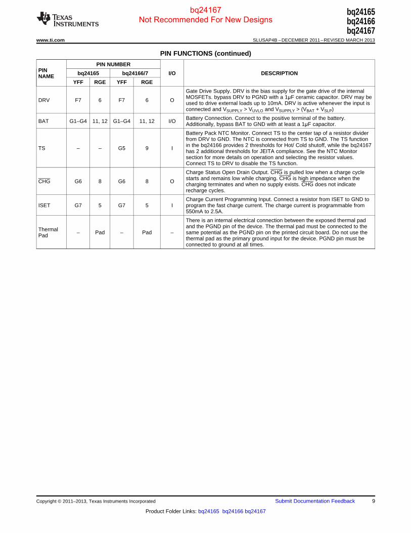
PIN FUNCTIONSPIN NUMBER
PIN bq24165 bq24166/7 I/O DESCRIPTIONNAMEYFF RGE YFF RGE
Input power supply. IN is connected to the external DC supply (AC adapter orIN A1–A4 21 A1–A4 21 I alternate power source). Bypass IN to PGND with at least a 1μF ceramic
capacitor.
USB Input Power Supply. USB is connected to the external DC supply (ACUSB A5–A7 22 A5–A7 22 I adapter or USB port). Bypass USB to PGND with at least a 1μF ceramic
capacitor.
Reverse Blocking MOSFET and High Side MOSFET Connection Point forHigh Power Input. Bypass PMIDI to GND with at least a 4.7μF ceramic
PMIDI B1–B4 20 B1–B4 20 O capacitor. Use caution when connecting an external load to PMIDI. ThePMIDI output is not current limited. Any short on PMIDI will result in damageto the IC.
Reverse Blocking MOSFET and High Side MOSFET Connection Point forUSB Input. Bypass PMIDU to GND with at least a 4.7μF ceramic capacitor.PMIDU B5–B7 23 B5–B7 23 O Use caution when connecting an external load to PMIDU. The PMIDU outputis not current limited. Any short on PMIDU will result in damage to the IC.
SW C1–C7 18 C1–C7 18 O Inductor Connection. Connect to the switched side of the external inductor.
Ground terminal. Connect to the thermal pad (for QFN only) and the groundPGND D1–D7 16, 17 D1–D7 16, 17 – plane of the circuit.
IN Input Current Limit Programming Input. Connect a resistor from ILIM toILIM E1 15 E1 15 I GND to program the input current limit for IN. The current limit is
programmable from 1A to 2.5A. ILIM has no effect on the USB input.
Input DPM Programming Input. Connect a resistor divider from IN to GNDwith VDPM connected to the center tap to program the Input Voltage based
VDPM E3 1 E3 1 I Dynamic Power Management (VIN-DPM) threshold. The input current isreduced to maintain the supply voltage at VIN-DPM. See the Input Voltagebased Dynamic Power Management section for a detailed explanation.
Charge Enable Input. CE is used to disable or enable the charge process. Alow logic level (0) enables charging and a high logic level (1) disablescharging. When charging is disabled, the SYS output remains in regulation,CE – – E4 24 I but BAT is disconnected from SYS. Supplement mode is still available if thesystem load demands cannot be met by the supply. BGATE is highimpedance when CE is high.
IUSB1 E5 4 E5 4 I USB Input Current Limit Programming Inputs. USB1, USB2 and USB3program the input current limit for the USB input. USB2.0 and USB3.0 currentIUSB2 E6 3 E6 3 Ilimits are available for easy implementation of these standards. Table 1shows the settings for these inputs. USB1, USB2 and USB3 have no effect onIUSB3 E2 2 E2 2 Ithe IN input.
CE1 E4 24 – – I JEITA Compliance Inputs. CE1 and CE2are used to change battery regulationand charge current regulation to comply with the JEITA charging standard.The charge voltage can be reduced by 140mV or the charge current may beCE2 G5 9 – – Ireduced to half the programmed value. See Table 2 for programming details.
High Side MOSFET Gate Driver Supply. Connect a 0.01μF ceramic capacitorBOOT E7 19 E7 19 I (voltage rating > 10V) from BOOT to SW to supply the gate drive for the high
side MOSFETs.
System Voltage Sense and Charger FET Connection. Connect SYS to theSYS F1–F4 13, 14 F1–F4 13, 14 I system output at the output bulk capacitors. Bypass SYS locally with at least
10μF. 47μF bypass capacitance is recommended for best transient response.
External Discharge MOSFET Gate Connection. BGATE drives an external P-Channel MOSFET to provide a very low resistance discharge path. Connect
BGATE F5 10 F5 10 O BGATE to the gate of the external MOSFET. BGATE is low during highimpedance mode and when no input is connected. BGATE is optional. Ifunused, leave BGATE unconnected.
Power Good Open Drain Output. PG is pulled low when a valid supply isconnected to either USB or IN. A valid supply is between VBAT+VSLP andPG F6 7 F6 7 O VOVP. If not supply is connected or the supply is out of this range, PG is highimpedance.
8 Submit Documentation Feedback Copyright © 2011–2013, Texas Instruments Incorporated
Product Folder Links: bq24165 bq24166 bq24167
bq24167 Not Recommended For New Designs
bq24165bq24166bq24167
www.ti.com SLUSAP4B –DECEMBER 2011–REVISED MARCH 2013
PIN FUNCTIONS (continued)
PIN NUMBERPIN bq24165 bq24166/7 I/O DESCRIPTIONNAME
YFF RGE YFF RGE
Gate Drive Supply. DRV is the bias supply for the gate drive of the internalMOSFETs. bypass DRV to PGND with a 1μF ceramic capacitor. DRV may beDRV F7 6 F7 6 O used to drive external loads up to 10mA. DRV is active whenever the input isconnected and VSUPPLY > VUVLO and VSUPPLY > (VBAT + VSLP)
Battery Connection. Connect to the positive terminal of the battery.BAT G1–G4 11, 12 G1–G4 11, 12 I/O Additionally, bypass BAT to GND with at least a 1μF capacitor.
Battery Pack NTC Monitor. Connect TS to the center tap of a resistor dividerfrom DRV to GND. The NTC is connected from TS to GND. The TS functionin the bq24166 provides 2 thresholds for Hot/ Cold shutoff, while the bq24167TS – – G5 9 I has 2 additional thresholds for JEITA compliance. See the NTC Monitorsection for more details on operation and selecting the resistor values.Connect TS to DRV to disable the TS function.
Charge Status Open Drain Output. CHG is pulled low when a charge cyclestarts and remains low while charging. CHG is high impedance when theCHG G6 8 G6 8 O charging terminates and when no supply exists. CHG does not indicaterecharge cycles.
Charge Current Programming Input. Connect a resistor from ISET to GND toISET G7 5 G7 5 I program the fast charge current. The charge current is programmable from
550mA to 2.5A.
There is an internal electrical connection between the exposed thermal padand the PGND pin of the device. The thermal pad must be connected to theThermal – Pad – Pad – same potential as the PGND pin on the printed circuit board. Do not use thePad thermal pad as the primary ground input for the device. PGND pin must beconnected to ground at all times.
Copyright © 2011–2013, Texas Instruments Incorporated Submit Documentation Feedback 9
Product Folder Links: bq24165 bq24166 bq24167
bq24167 Not Recommended For New Designs
SW
SYS
BAT
BGATE
DRV
PGND
PMIDU
USB
IUSB1
BOOT
1mF 4.7mF
PMIDI
IN
System
Load
PG
1mF 4.7mF
10mF
1mF
VBUS
D+
D-
GND
ADAPTER
IUSB2
HOST
0.01mF
CHG
ILIM
VDPM
ISET
IUSB3
TEMPPACK+
PACK-
GPIO
GPIO
GPIO
bq24166
bq24167
TS
VDRV
CE GPIO
SW
SYS
BAT
BGATE
DRV
PGND
PMIDU
USB
IUSB1
CE2
BOOT
1mF
4.7mF
PMIDI
IN
System
Load
GSM
PA
PG
1mF 4.7mF
10mF
1mF
VBUSD+
D-
GND
ADAPTER
IUSB2
HOST
GPIO
0.01mF
CHG
ILIM
VDPM
ISET
IUSB3
CE1
TEMPPACK+
PACK-
GPIO
GPIO
GPIO
GPIO
NTC
MONITOR
bq24165
bq24165bq24166bq24167SLUSAP4B –DECEMBER 2011–REVISED MARCH 2013 www.ti.com
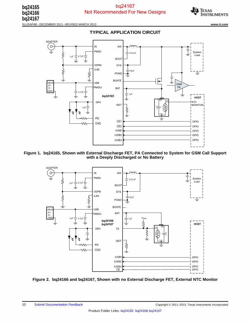
TYPICAL APPLICATION CIRCUIT
Figure 1. bq24165, Shown with External Discharge FET, PA Connected to System for GSM Call Supportwith a Deeply Discharged or No Battery
Figure 2. bq24166 and bq24167, Shown with no External Discharge FET, External NTC Monitor
10 Submit Documentation Feedback Copyright © 2011–2013, Texas Instruments Incorporated
Product Folder Links: bq24165 bq24166 bq24167
bq24167 Not Recommended For New Designs
1 A/div
2 V/div
2 V/div
20 ms/div
VCHG
VBAT
VSYS
IBAT
1 A/div
2 V/div
2 V/div
200 ms/div
VCHG
VBAT
VSYS
IBAT
bq24165bq24166bq24167
www.ti.com SLUSAP4B –DECEMBER 2011–REVISED MARCH 2013
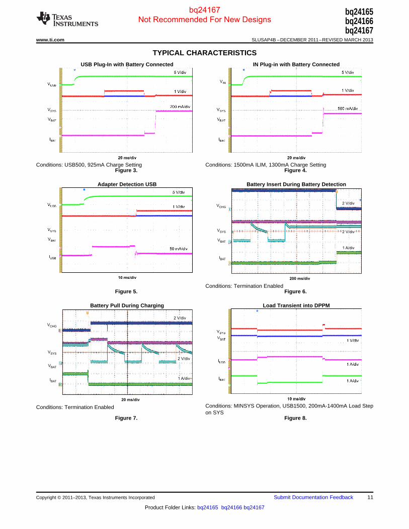
TYPICAL CHARACTERISTICS
USB Plug-In with Battery Connected IN Plug-in with Battery Connected
Conditions: USB500, 925mA Charge Setting Conditions: 1500mA ILIM, 1300mA Charge SettingFigure 3. Figure 4.
Adapter Detection USB Battery Insert During Battery Detection
Conditions: Termination EnabledFigure 5. Figure 6.
Battery Pull During Charging Load Transient into DPPM
Conditions: MINSYS Operation, USB1500, 200mA-1400mA Load StepConditions: Termination Enabledon SYS
Figure 7. Figure 8.
Copyright © 2011–2013, Texas Instruments Incorporated Submit Documentation Feedback 11
Product Folder Links: bq24165 bq24166 bq24167
bq24167 Not Recommended For New Designs

3.4
3.45
3.5
3.55
3.6
3.65
3.7
3.75
3.8
3.85
3.9
−50 0 50 100 150Temperature (°C)
SY
SR
EG
and
MIN
SY
S R
egul
atio
n (V
)
SYSREG Regulation MINSYS Regulation
G003
4.19
4.192
4.194
4.196
4.198
4.2
4.202
4.204
4.206
4.208
4.21
0 25 50 75 100 125Temperature (°C)
Bat
tery
Reg
ulat
ion
(V)
G004
0
10
20
30
40
50
60
70
80
90
100
0.1 1 3System Current (A)
Effi
cien
cy (
%)
VIN = 5 VVIN = 7 VVIN = 9 V
G001
0
10
20
30
40
50
60
70
80
90
100
0.1 1 2System Current (A)
Effi
cien
cy (
%)
VUSB = 5 VVUSB = 6 V
G002
500 mA/div
1 A/div
1 V/div
10 ms/div
VBAT
IUSB
VSYS
IBAT
4 ms/div
VCHG
VSW
VUSB
IBAT
500 mA/div
5 V/div
5 V/div
5 V/div
bq24165bq24166bq24167SLUSAP4B –DECEMBER 2011–REVISED MARCH 2013 www.ti.com
TYPICAL CHARACTERISTICS (continued)OVP Fault
Load Transient into Supplement Mode USB Input
Conditions: MINSYS Operation, USB500, 200mA - 1400mA LoadStep on SYS
Figure 9. Figure 10.
IN Efficiency USB Efficiency
Conditions: Charge Disabled, SYS loaded, VBATREG = 3.6V, IN2500 Conditions: Charge Disabled, SYS loaded, VBATREG = 3.6V, USB1500ILIM ILIM
Figure 11. Figure 12.
SYSREG and MINSYS Regulation vs. Temperature Battery Regulation vs Temperature
Conditions: VBAT = 3V Conditions: VBATREG = 4.2V, No load, Termination DisabledFigure 13. Figure 14.
12 Submit Documentation Feedback Copyright © 2011–2013, Texas Instruments Incorporated
Product Folder Links: bq24165 bq24166 bq24167
bq24167 Not Recommended For New Designs
0.05
0.051
0.052
0.053
0.054
0.055
0 0.5 1 1.5 2 2.5 3Battery Voltage (V)
I BA
TS
HR
T (
A)
G009
10
10.1
10.2
10.3
10.4
10.5
10.6
10.7
−50 0 50 100 150Temperature (°C)
10.5
V O
VP
Thr
esho
ld (
V)
Falling EdgeRising Edge
G007
2
2.01
2.02
2.03
2.04
2.05
2.06
2.07
2.08
2.09
2.1
2 2.5 3 3.5 4 4.5Battery Voltage (V)
Cha
rge
Cur
rent
(A
)
G008
0
100
200
300
400
500
600
700
−50 0 50 100 150Temperature (°C)
US
B In
put C
urre
nt L
imit
(mA
)
USB100 Current LimitUSB500 Current Limit
G005
6
6.1
6.2
6.3
6.4
6.5
6.6
6.7
−50 0 50 100 150Temperature (°C)
6.5
V O
VP
Thr
esho
ld (
V)
Falling EdgeRising Edge
G006
bq24165bq24166bq24167
www.ti.com SLUSAP4B –DECEMBER 2011–REVISED MARCH 2013
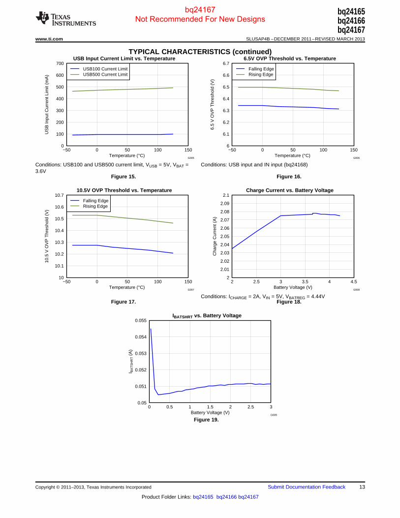
TYPICAL CHARACTERISTICS (continued)USB Input Current Limit vs. Temperature 6.5V OVP Threshold vs. Temperature
Conditions: USB100 and USB500 current limit, VUSB = 5V, VBAT = Conditions: USB input and IN input (bq24168)3.6V
Figure 15. Figure 16.
10.5V OVP Threshold vs. Temperature Charge Current vs. Battery Voltage
Conditions: ICHARGE = 2A, VIN = 5V, VBATREG = 4.44VFigure 17. Figure 18.
IBATSHRT vs. Battery Voltage
Figure 19.
Copyright © 2011–2013, Texas Instruments Incorporated Submit Documentation Feedback 13
Product Folder Links: bq24165 bq24166 bq24167
bq24167 Not Recommended For New Designs

Termination
RegulationCurrent
Regulation
voltage
Precharge
PhaseCurrent Regulation
Phase
Voltage Regulation
Phase
Charge Current
Battery
Voltage
VSYS
(3.6V)
System Voltage
Linear Charge
to Maintain
Minimum
System
Voltage
VBATSHORT
IBATSHORT
50mA Linear Charge
to Close Pack
Protector
Battery FET is ON
Battery
FET
is OFF
bq24165bq24166bq24167SLUSAP4B –DECEMBER 2011–REVISED MARCH 2013 www.ti.com
DETAILED DESCRIPTION
CHARGE MODE OPERATION
Charge ProfileCharging is done through the internal battery MOSFET. When the battery voltage is above 3.5V, the systemoutput (SYS) is connected to the battery to maximize the charging efficiency. There are 6 loops that influence thecharge current; constant current loop (CC), constant voltage loop (CV), input current loop, thermal regulationloop, minimum system voltage loop (MINSYS) and input voltage dynamic power management loop (VINDPM).During the charging process, all six loops are enabled and the dominate one takes control. The bq24165/6/7supports a precision Li-Ion or Li-Polymer charging system for single-cell applications. The minimum systemoutput feature regulates the system voltage to a minimum of VSYS(REG), so that startup is enabled even for amissing or deeply discharged battery. Figure 20 shows a typical charge profile including the minimum systemoutput voltage feature.
Figure 20. Typical Charging Profile of bq24165/6/7
PWM CONTROLLER IN CHARGE MODE
The bq24165/6/7 provides an integrated, fixed 1.5 MHz frequency voltage-mode converter to power the systemand supply the charge current. The voltage loop is internally compensated and provides enough phase marginfor stable operation, allowing the use of small ceramic capacitors with very low ESR.
The bq24165/6/7 input scheme prevents battery discharge when the supply voltages is lower than VBAT andalso isolates the two inputs from each other. The high-side N-MOSFET (Q1/Q2) switches to control the powerdelivered to the output. The DRV LDO supplies the gate drive for the internal MOSFETs. The high side FETs aresupplied through a boot strap circuit with external boot-strap capacitor is used to boost up the gate drive voltagefor Q1/Q2.
Both inputs are protected by a cycle-by-cycle current limit that is sensed through the internal MOSFETs for Q1and Q2. The threshold for the current limit is set to a nominal 5-A peak current. The inputs also utilize an inputcurrent limit that limits the current from the power source.
14 Submit Documentation Feedback Copyright © 2011–2013, Texas Instruments Incorporated
Product Folder Links: bq24165 bq24166 bq24167
bq24167 Not Recommended For New Designs
ISETISET
CHARGE
KR =
I
bq24165bq24166bq24167
www.ti.com SLUSAP4B –DECEMBER 2011–REVISED MARCH 2013
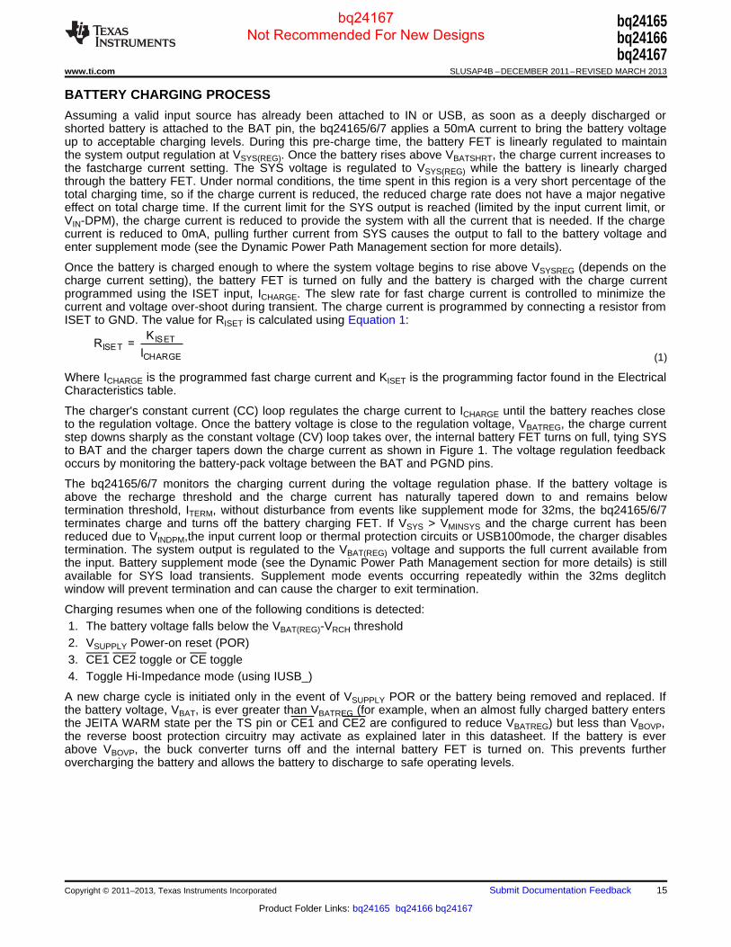
BATTERY CHARGING PROCESS
Assuming a valid input source has already been attached to IN or USB, as soon as a deeply discharged orshorted battery is attached to the BAT pin, the bq24165/6/7 applies a 50mA current to bring the battery voltageup to acceptable charging levels. During this pre-charge time, the battery FET is linearly regulated to maintainthe system output regulation at VSYS(REG). Once the battery rises above VBATSHRT, the charge current increases tothe fastcharge current setting. The SYS voltage is regulated to VSYS(REG) while the battery is linearly chargedthrough the battery FET. Under normal conditions, the time spent in this region is a very short percentage of thetotal charging time, so if the charge current is reduced, the reduced charge rate does not have a major negativeeffect on total charge time. If the current limit for the SYS output is reached (limited by the input current limit, orVIN-DPM), the charge current is reduced to provide the system with all the current that is needed. If the chargecurrent is reduced to 0mA, pulling further current from SYS causes the output to fall to the battery voltage andenter supplement mode (see the Dynamic Power Path Management section for more details).
Once the battery is charged enough to where the system voltage begins to rise above VSYSREG (depends on thecharge current setting), the battery FET is turned on fully and the battery is charged with the charge currentprogrammed using the ISET input, ICHARGE. The slew rate for fast charge current is controlled to minimize thecurrent and voltage over-shoot during transient. The charge current is programmed by connecting a resistor fromISET to GND. The value for RISET is calculated using Equation 1:
(1)
Where ICHARGE is the programmed fast charge current and KISET is the programming factor found in the ElectricalCharacteristics table.
The charger's constant current (CC) loop regulates the charge current to ICHARGE until the battery reaches closeto the regulation voltage. Once the battery voltage is close to the regulation voltage, VBATREG, the charge currentstep downs sharply as the constant voltage (CV) loop takes over, the internal battery FET turns on full, tying SYSto BAT and the charger tapers down the charge current as shown in Figure 1. The voltage regulation feedbackoccurs by monitoring the battery-pack voltage between the BAT and PGND pins.
The bq24165/6/7 monitors the charging current during the voltage regulation phase. If the battery voltage isabove the recharge threshold and the charge current has naturally tapered down to and remains belowtermination threshold, ITERM, without disturbance from events like supplement mode for 32ms, the bq24165/6/7terminates charge and turns off the battery charging FET. If VSYS > VMINSYS and the charge current has beenreduced due to VINDPM,the input current loop or thermal protection circuits or USB100mode, the charger disablestermination. The system output is regulated to the VBAT(REG) voltage and supports the full current available fromthe input. Battery supplement mode (see the Dynamic Power Path Management section for more details) is stillavailable for SYS load transients. Supplement mode events occurring repeatedly within the 32ms deglitchwindow will prevent termination and can cause the charger to exit termination.
Charging resumes when one of the following conditions is detected:1. The battery voltage falls below the VBAT(REG)-VRCH threshold2. VSUPPLY Power-on reset (POR)3. CE1 CE2 toggle or CE toggle4. Toggle Hi-Impedance mode (using IUSB_)
A new charge cycle is initiated only in the event of VSUPPLY POR or the battery being removed and replaced. Ifthe battery voltage, VBAT, is ever greater than VBATREG (for example, when an almost fully charged battery entersthe JEITA WARM state per the TS pin or CE1 and CE2 are configured to reduce VBATREG) but less than VBOVP,the reverse boost protection circuitry may activate as explained later in this datasheet. If the battery is everabove VBOVP, the buck converter turns off and the internal battery FET is turned on. This prevents furtherovercharging the battery and allows the battery to discharge to safe operating levels.
Copyright © 2011–2013, Texas Instruments Incorporated Submit Documentation Feedback 15
Product Folder Links: bq24165 bq24166 bq24167
bq24167 Not Recommended For New Designs

bq24165bq24166bq24167SLUSAP4B –DECEMBER 2011–REVISED MARCH 2013 www.ti.com
BATTERY DETECTION
When termination conditions are met, a battery detection cycle is started. During battery detection, IDETECT ispulled from VBAT for tDETECT to verify there is a battery. If the battery voltage remains above VDETECT for the fullduration of tDETECT, a battery is determined to present and the IC enters “Charge Done”. If VBAT falls belowVDETECT, battery detection continues. The next cycle of battery detection, the bq2416x turns on IBATSHORT fortDETECT. If VBAT rises to VDETECT, the current source is turned offand after tDETECT, the battery detection continuesthrough another current sink cycle. Battery detection continues until charge is disabled or a battery is detected.Once a battery is detected, the fault status clears and a new charge cycle begins. Figures 6 and 7 show theoscillation on VBAT prior to battery insertion and after battery removal. Battery detection is disabled whentermination is disabled.
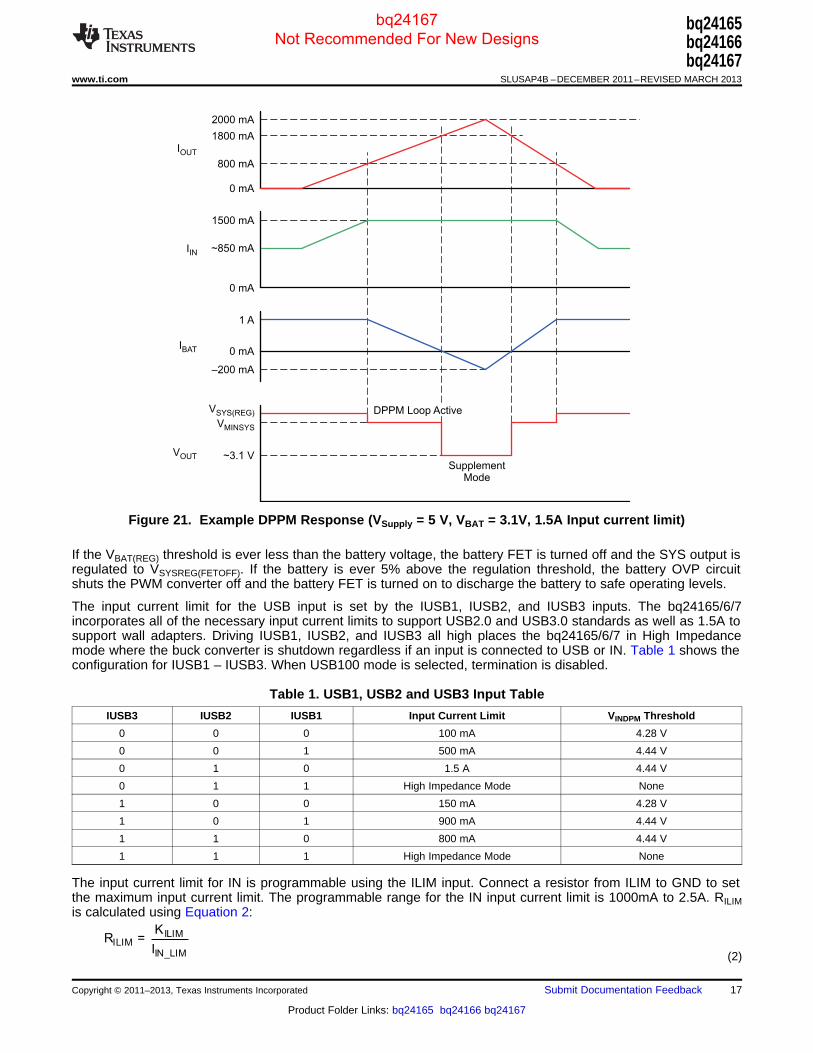
DYNAMIC POWER PATH MANAGEMENT
The bq24165/6/7 features a SYS output that powers the external system load connected to the battery. Thisoutput is active whenever a source is connected to IN, USB or BAT. The following sections discuss the behaviorof SYS with a source connected to the supply (IN or USB) or a battery source only.
INPUT SOURCE CONNECTED
When a source is connected to IN or USB, and the bq24165/6/7 is enabled, the buck converter starts up. Ifcharging is enabled using CE1 and CE2(bq24165) or CE (bq24166/7), the charge cycle is initiated. When VBAT >3.5V, the internal battery FET is turned on and the SYS output is connected to VBAT. If the SYS voltage falls toVSYS(REG), it is regulated to that point to maintain the system output even with a deeply discharged or absentbattery. In this mode, the SYS output voltage is regulated by the buck converter and the battery FET is linearlyregulated to regulate the charge current into the battery. The current from the supply is shared between chargingthe battery and powering the system load at SYS. The dynamic power path management (DPPM) circuitry of thebq24165/6/7 monitors the SYS voltage continuously. If VSYS falls to VMINSYS, the DPPM circuit adjusts chargecurrent to maintain the load on SYS while preventing the system voltage from crashing. If the charge current isreduced to zero and the load increases further, the bq24165/6/7 enters battery supplement mode. Duringsupplement mode, the battery FET is turned on and the battery supplements the system load. When the chargecurrent is reduced by the DPPM regulation loop, the safety timer runs at half speed, so that it is twice a long.This prevents false safety timer faults. See the Safety Timer section for more details.
16 Submit Documentation Feedback Copyright © 2011–2013, Texas Instruments Incorporated
Product Folder Links: bq24165 bq24166 bq24167
bq24167 Not Recommended For New Designs
ILIMILIM
IN_LIM
KR =
I
0 mA
0 mA
VSYS(REG)
VOUT
IBAT
IIN
IOUT
VMINSYS
~3.1 VSupplement
Mode
800 mA
1800 mA
2000 mA
–200 mA
1 A
1500 mA
~850 mA
0 mA
DPPM Loop Active
bq24165bq24166bq24167
www.ti.com SLUSAP4B –DECEMBER 2011–REVISED MARCH 2013
Figure 21. Example DPPM Response (VSupply = 5 V, VBAT = 3.1V, 1.5A Input current limit)
If the VBAT(REG) threshold is ever less than the battery voltage, the battery FET is turned off and the SYS output isregulated to VSYSREG(FETOFF). If the battery is ever 5% above the regulation threshold, the battery OVP circuitshuts the PWM converter off and the battery FET is turned on to discharge the battery to safe operating levels.
The input current limit for the USB input is set by the IUSB1, IUSB2, and IUSB3 inputs. The bq24165/6/7incorporates all of the necessary input current limits to support USB2.0 and USB3.0 standards as well as 1.5A tosupport wall adapters. Driving IUSB1, IUSB2, and IUSB3 all high places the bq24165/6/7 in High Impedancemode where the buck converter is shutdown regardless if an input is connected to USB or IN. Table 1 shows theconfiguration for IUSB1 – IUSB3. When USB100 mode is selected, termination is disabled.
Table 1. USB1, USB2 and USB3 Input Table
IUSB3 IUSB2 IUSB1 Input Current Limit VINDPM Threshold
0 0 0 100 mA 4.28 V
0 0 1 500 mA 4.44 V
0 1 0 1.5 A 4.44 V
0 1 1 High Impedance Mode None
1 0 0 150 mA 4.28 V
1 0 1 900 mA 4.44 V
1 1 0 800 mA 4.44 V
1 1 1 High Impedance Mode None
The input current limit for IN is programmable using the ILIM input. Connect a resistor from ILIM to GND to setthe maximum input current limit. The programmable range for the IN input current limit is 1000mA to 2.5A. RILIMis calculated using Equation 2:
(2)
Copyright © 2011–2013, Texas Instruments Incorporated Submit Documentation Feedback 17
Product Folder Links: bq24165 bq24166 bq24167
bq24167 Not Recommended For New Designs
bq24165bq24166bq24167SLUSAP4B –DECEMBER 2011–REVISED MARCH 2013 www.ti.com
Where IIN_LIM is the programmed input current limit and KILIM is the programming factor found in the ElectricalCharacteristics table.
The bq24165/6/7 manages the dual input supply paths as well. The IN input has precedence when valid suppliesare connected to both inputs. The two inputs are always isolated from one another. The bq24165/6/7 alwaysseeks to charge from a valid source. For example, if a valid source is connected to USB and a source isconnected to IN that is greater than the OVP threshold, the USB source is used to charge the battery. In thiscase, both the USB source and the battery would be isolated from the OVP source connected to the IN input.
BATTERY ONLY CONNECTED
When the battery is connected with no input source, the internal battery FET is turned on similar to supplementmode. In this mode, the current is not regulated; however, there is a short circuit current limit. If the short circuitlimit is reached, the battery FET is turned off for the deglitch time. After the deglitch time, the battery FET isturned on in order to determine if the short has been removed. If not, the FET turns off and the process repeatsuntil the short is removed.
EXTERNAL BATTERY DISCHARGE FET (BGATE)
The bq24165/6/7 contains a MOSFET driver to drive an external P-Channel MOSFET between the battery andthe system output. This external FET provides a low impedance path to supply the system from the battery.Connect BGATE to the gate of the external discharge MOSFET. BGATE is on under the following conditions:1. No valid input supply connected.2. IUSB1=IUSB2=IUSB3=high (High Impedance Mode)
This FET is optional and runs in parallel with the internal charge FET during discharge. Note that this FET is notprotected by the short circuit current limit.
SAFETY TIMER
At the beginning of charging process, the bq24165/6/7 starts the 6 hour safety timer. This timer is active duringthe entire charging process. If charging has not terminated before the safety timer expires, the charge cycle isterminated and the battery FET is turned off. To clear the safety timer fault, charging must be resumed by usingCE1 and CE2 (bq24165) or CE(bq24166/7) or High Impedance mode or a new charge cycle started by VSUPPLYPOR or battery remove and replace.
During the fast charge (CC) phase, several events increase the timer duration by 2X.1. The system load current reduces the available charging current.2. The input current needed for the fast charge current is limited by the input current loop.3. The input current is reduced because the VINDPM loop is preventing the supply from crashing.4. The device has entered thermal regulation because the IC junction temperature has exceeded TJ(REG).5. The CEx bits are reducing ICHARGE or VBAT.6. The battery voltage is less than VBATSHORT.7. The battery has entered the JEITA WARM or COLD state via the TS pin (bq24166/6) or CE1/CE2
(bq24165)configuration.
During these events, the timer is slowed by half to extend the timer and prevent any false timer faults. Starting anew charge cycle by VSUPPLY POR or removing/replacing the battery or resuming a charge by toggling theCE1/CE2(bq24165) or CE(bq24166/7) pins, resets the safety timer. Additionally, thermal shutdown events causethe safety timer to reset.
18 Submit Documentation Feedback Copyright © 2011–2013, Texas Instruments Incorporated
Product Folder Links: bq24165 bq24166 bq24167
bq24167 Not Recommended For New Designs
Maximum Charge Current: 1 C
Maximum Charge Voltage: 4.25 V(4.2 V Typical)
0.5 C
4.15 V Maximum
T1(0°C)
T2(10°C)
T3(45°C)
T4(50°C)
T5(60°C)
4.10 V Maximum
bq24165bq24166bq24167
www.ti.com SLUSAP4B –DECEMBER 2011–REVISED MARCH 2013
LDO OUTPUT (DRV)
The bq24165/6/7 contains a linear regulator (DRV) that is used to supply the internal MOSFET drivers and othercircuitry. Additionally, DRV supplies up to 10mA external loads to power the STAT LED or the USB transceivercircuitry. The maximum value of the DRV output is 5.45V so it is ideal to protect voltage sensitive USB circuits.The LDO is on whenever a supply is connected to the IN or USB inputs of the bq24165/166. The DRV isdisabled under the following conditions:1. VSUPPLY < UVLO2. VSUPPLY - VBAT< VSLP
3. Thermal Shutdown
CHARGE PARAMETER SELECTOR INPUTS (CE1, CE2, bq24165)
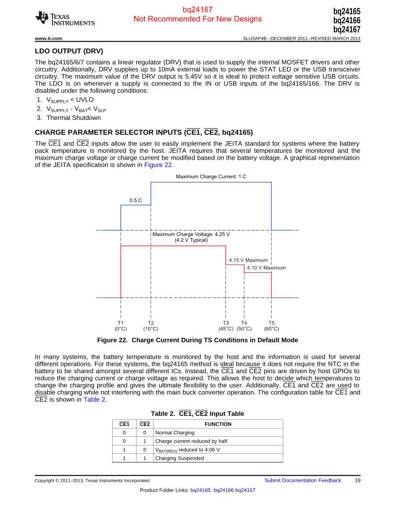
The CE1 and CE2 inputs allow the user to easily implement the JEITA standard for systems where the batterypack temperature is monitored by the host. JEITA requires that several temperatures be monitored and themaximum charge voltage or charge current be modified based on the battery voltage. A graphical representationof the JEITA specification is shown in Figure 22.
Figure 22. Charge Current During TS Conditions in Default Mode
In many systems, the battery temperature is monitored by the host and the information is used for severaldifferent operations. For these systems, the bq24165 method is ideal because it does not require the NTC in thebattery to be shared amongst several different ICs. Instead, the CE1 and CE2 pins are driven by host GPIOs toreduce the charging current or charge voltage as required. This allows the host to decide which temperatures tochange the charging profile and gives the ultimate flexibility to the user. Additionally, CE1 and CE2 are used todisable charging while not interfering with the main buck converter operation. The configuration table for CE1 andCE2 is shown in Table 2.
Table 2. CE1, CE2 Input Table
CE1 CE2 FUNCTION
0 0 Normal Charging
0 1 Charge current reduced by half
1 0 VBAT(REG) reduced to 4.06 V
1 1 Charging Suspended
Copyright © 2011–2013, Texas Instruments Incorporated Submit Documentation Feedback 19
Product Folder Links: bq24165 bq24166 bq24167
bq24167 Not Recommended For New Designs

RLO 0.383 RHIRWARM =
RLO RLO 0.383 RHI 0.383
´ ´
- ´ - ´
RLO 0.564 RHIRCOOL =
RLO RLO 0.564 RHI 0.564
´ ´
- ´ - ´
DRV
COLD
V1
VRHI =
1 1+
RLO RCOLD
-
DRV
COLD HOT
DRV DRV
HOT COLD
1 1V RCOLD RHOT
V VRLO =
V VRHOT 1 RCOLD 1
V V
é ù´ ´ ´ -ê ú
ë û
é ù é ù´ - - ´ -ê ú ê ú
ë û ë û
bq24165bq24166bq24167SLUSAP4B –DECEMBER 2011–REVISED MARCH 2013 www.ti.com
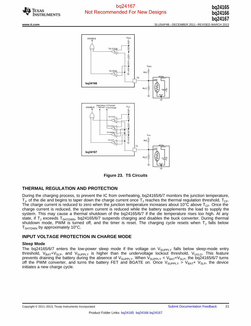
EXTERNAL NTC MONITORING (TS, bq24166/7)
The bq24166 and bq24167 provide a flexible, voltage based TS input for monitoring the battery pack NTCthermistor. The voltage at TS is monitored to determine that the battery is at a safe temperature during charging.For the bq24166, two temperature thresholds are monitored; the cold battery threshold (TNTC < 0°C) and the hotbattery threshold (TNTC > 60°C). These temperatures correspond to the VCOLD and VHOT thresholds. Charging issuspended and timers are suspended when VTS < VHOT or VTS > VCOLD.
To satisfy the JEITA requirements, the bq24167 monitors four temperature thresholds; the cold battery threshold(TNTC < 0°C), the cool battery threshold (0°C < TNTC < 10°C), the warm battery threshold (45°C < TNTC < 60°C)and the hot battery threshold (TNTC > 60°C). These temperatures correspond to the VCOLD, VCOOL, VWARM, andVHOT thresholds. As with the bq24166, charging is suspended and timers are suspended when VTS < VHOT or VTS> VCOLD. When VHOT < VTS < VWARM, the battery regulation voltage is reduced by 140mV from the programmedregulation threshold. When VCOOL < VTS < VCOLD, the charging current is reduced to half of the programmedcharge current.
The TS function is voltage based for maximum flexibility. Connect a resistor divider from DRV to GND with TSconnected to the center tap to set the threshold. The connections are shown in Figure 24. The resistor values arecalculated using the following equations:
(3)
(4)
Where:VCOLD = 0.60 × VDRV
VHOT = 0.30 × VDRV
Where RHOT is the NTC resistance at the hot temperature and RCOLD is the NTC resistance at coldtemperature.
For the bq24167, the WARM and COOL thresholds are not independently programmable. The COOL andWARM NTC resistances for a selected resistor divider are calculated using the following equations:
(5)
(6)
20 Submit Documentation Feedback Copyright © 2011–2013, Texas Instruments Incorporated
Product Folder Links: bq24165 bq24166 bq24167
bq24167 Not Recommended For New Designs
DISABLE
VDRV
TEMPPACK+
PACK-
+
+
VDRV
TS COLD
TS HOT
TS
bq24166
RHI
RLO
DISABLE
VDRV
TEMPPACK+
PACK-
+
+
+
+
VDRV
TS COLD
TS HOT
TS WARM
TS COOL
VBAT(REG)
–140 mV
bq24167
RHI
RLO
1xCharge/0.5xCharge
TS
bq24165bq24166bq24167
www.ti.com SLUSAP4B –DECEMBER 2011–REVISED MARCH 2013
Figure 23. TS Circuits
THERMAL REGULATION AND PROTECTION
During the charging process, to prevent the IC from overheating, bq24165/6/7 monitors the junction temperature,TJ, of the die and begins to taper down the charge current once TJ reaches the thermal regulation threshold, TCF.The charge current is reduced to zero when the junction temperature increases about 10°C above TCF. Once thecharge current is reduced, the system current is reduced while the battery supplements the load to supply thesystem. This may cause a thermal shutdown of the bq24165/6/7 if the die temperature rises too high. At anystate, if TJ exceeds TSHTDWN, bq24165/6/7 suspends charging and disables the buck converter. During thermalshutdown mode, PWM is turned off, and the timer is reset. The charging cycle resets when TJ falls belowTSHTDWN by approximately 10°C.
INPUT VOLTAGE PROTECTION IN CHARGE MODE
Sleep ModeThe bq24165/6/7 enters the low-power sleep mode if the voltage on VSUPPLY falls below sleep-mode entrythreshold, VBAT+VSLP, and VSUPPLY is higher than the undervoltage lockout threshold, VUVLO. This featureprevents draining the battery during the absence of VSUPPLY. When VSUPPLY < VBAT+VSLP, the bq24165/6/7 turnsoff the PWM converter, and turns the battery FET and BGATE on. Once VSUPPLY > VBAT+ VSLP, the deviceinitiates a new charge cycle.
Copyright © 2011–2013, Texas Instruments Incorporated Submit Documentation Feedback 21
Product Folder Links: bq24165 bq24166 bq24167
bq24167 Not Recommended For New Designs
( )INDPM DPM
DPM
10 kΩ V VRTOP =
V
´ -
V
5 V Adapterrated for 750 mA
IN
IIN
VSYS
IBAT
ISYS
bq24165bq24166bq24167SLUSAP4B –DECEMBER 2011–REVISED MARCH 2013 www.ti.com
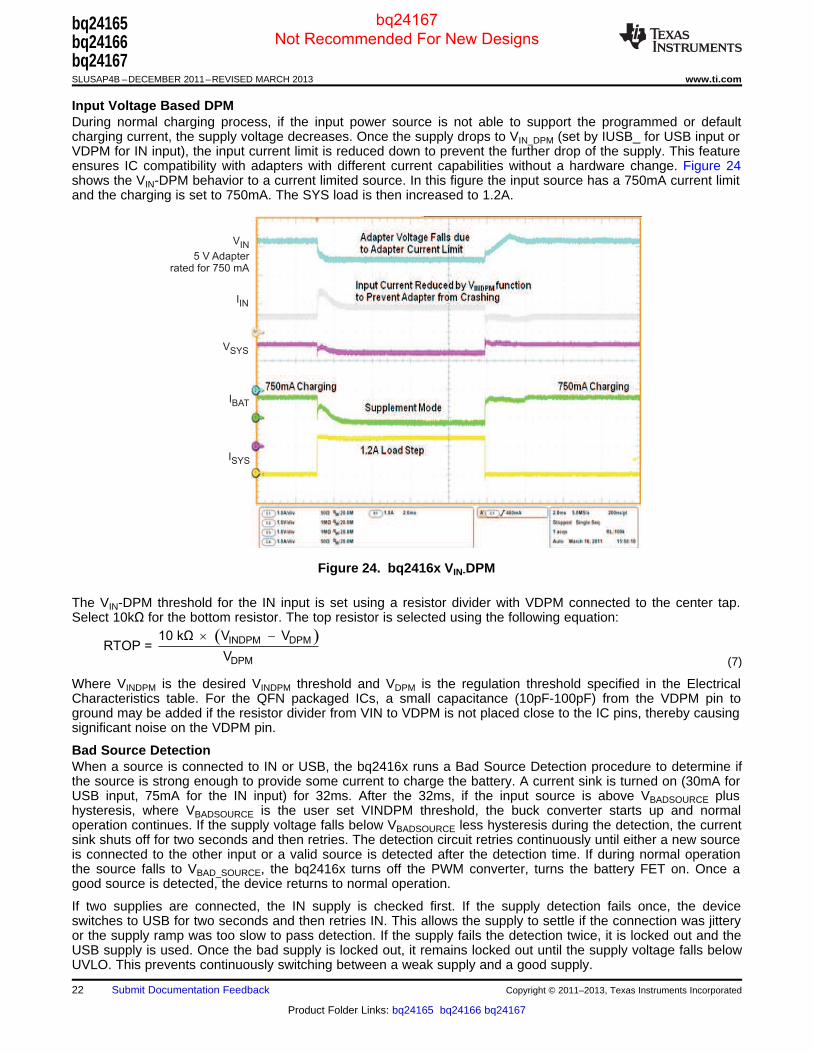
Input Voltage Based DPMDuring normal charging process, if the input power source is not able to support the programmed or defaultcharging current, the supply voltage decreases. Once the supply drops to VIN_DPM (set by IUSB_ for USB input orVDPM for IN input), the input current limit is reduced down to prevent the further drop of the supply. This featureensures IC compatibility with adapters with different current capabilities without a hardware change. Figure 24shows the VIN-DPM behavior to a current limited source. In this figure the input source has a 750mA current limitand the charging is set to 750mA. The SYS load is then increased to 1.2A.
Figure 24. bq2416x VIN-DPM
The VIN-DPM threshold for the IN input is set using a resistor divider with VDPM connected to the center tap.Select 10kΩ for the bottom resistor. The top resistor is selected using the following equation:
(7)
Where VINDPM is the desired VINDPM threshold and VDPM is the regulation threshold specified in the ElectricalCharacteristics table. For the QFN packaged ICs, a small capacitance (10pF-100pF) from the VDPM pin toground may be added if the resistor divider from VIN to VDPM is not placed close to the IC pins, thereby causingsignificant noise on the VDPM pin.
Bad Source DetectionWhen a source is connected to IN or USB, the bq2416x runs a Bad Source Detection procedure to determine ifthe source is strong enough to provide some current to charge the battery. A current sink is turned on (30mA forUSB input, 75mA for the IN input) for 32ms. After the 32ms, if the input source is above VBADSOURCE plushysteresis, where VBADSOURCE is the user set VINDPM threshold, the buck converter starts up and normaloperation continues. If the supply voltage falls below VBADSOURCE less hysteresis during the detection, the currentsink shuts off for two seconds and then retries. The detection circuit retries continuously until either a new sourceis connected to the other input or a valid source is detected after the detection time. If during normal operationthe source falls to VBAD_SOURCE, the bq2416x turns off the PWM converter, turns the battery FET on. Once agood source is detected, the device returns to normal operation.
If two supplies are connected, the IN supply is checked first. If the supply detection fails once, the deviceswitches to USB for two seconds and then retries IN. This allows the supply to settle if the connection was jitteryor the supply ramp was too slow to pass detection. If the supply fails the detection twice, it is locked out and theUSB supply is used. Once the bad supply is locked out, it remains locked out until the supply voltage falls belowUVLO. This prevents continuously switching between a weak supply and a good supply.
22 Submit Documentation Feedback Copyright © 2011–2013, Texas Instruments Incorporated
Product Folder Links: bq24165 bq24166 bq24167
bq24167 Not Recommended For New Designs
bq24165bq24166bq24167
www.ti.com SLUSAP4B –DECEMBER 2011–REVISED MARCH 2013
Input Over-Voltage ProtectionThe bq24165/6/7 provides over-voltage protection on the input that protects downstream circuitry. The built-ininput over-voltage protection to protect the device and other components against damage from overvoltage onthe input supply (Voltage from VUSB or VIN to PGND). When VSUPPLY > VOVP, the bq24165/6/7 turns off the PWMconverter, suspends the charging cycle and turns the battery FET and BGATE on. Once the OVP fault isremoved, the device returns to the operation it was in prior to the OVP fault.
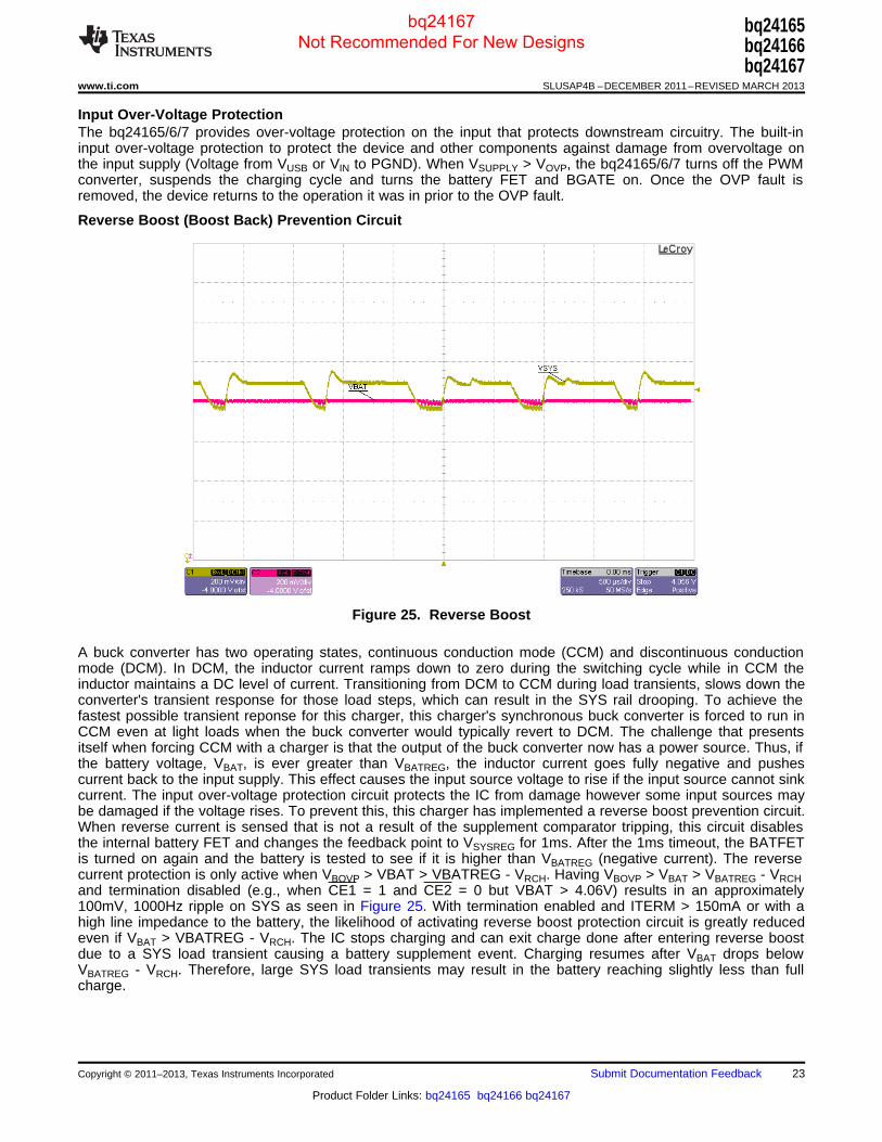
Reverse Boost (Boost Back) Prevention Circuit
Figure 25. Reverse Boost
A buck converter has two operating states, continuous conduction mode (CCM) and discontinuous conductionmode (DCM). In DCM, the inductor current ramps down to zero during the switching cycle while in CCM theinductor maintains a DC level of current. Transitioning from DCM to CCM during load transients, slows down theconverter's transient response for those load steps, which can result in the SYS rail drooping. To achieve thefastest possible transient reponse for this charger, this charger's synchronous buck converter is forced to run inCCM even at light loads when the buck converter would typically revert to DCM. The challenge that presentsitself when forcing CCM with a charger is that the output of the buck converter now has a power source. Thus, ifthe battery voltage, VBAT, is ever greater than VBATREG, the inductor current goes fully negative and pushescurrent back to the input supply. This effect causes the input source voltage to rise if the input source cannot sinkcurrent. The input over-voltage protection circuit protects the IC from damage however some input sources maybe damaged if the voltage rises. To prevent this, this charger has implemented a reverse boost prevention circuit.When reverse current is sensed that is not a result of the supplement comparator tripping, this circuit disablesthe internal battery FET and changes the feedback point to VSYSREG for 1ms. After the 1ms timeout, the BATFETis turned on again and the battery is tested to see if it is higher than VBATREG (negative current). The reversecurrent protection is only active when VBOVP > VBAT > VBATREG - VRCH. Having VBOVP > VBAT > VBATREG - VRCHand termination disabled (e.g., when CE1 = 1 and CE2 = 0 but VBAT > 4.06V) results in an approximately100mV, 1000Hz ripple on SYS as seen in Figure 25. With termination enabled and ITERM > 150mA or with ahigh line impedance to the battery, the likelihood of activating reverse boost protection circuit is greatly reducedeven if VBAT > VBATREG - VRCH. The IC stops charging and can exit charge done after entering reverse boostdue to a SYS load transient causing a battery supplement event. Charging resumes after VBAT drops belowVBATREG - VRCH. Therefore, large SYS load transients may result in the battery reaching slightly less than fullcharge.
Copyright © 2011–2013, Texas Instruments Incorporated Submit Documentation Feedback 23
Product Folder Links: bq24165 bq24166 bq24167
bq24167 Not Recommended For New Designs

bq24165bq24166bq24167SLUSAP4B –DECEMBER 2011–REVISED MARCH 2013 www.ti.com
STATUS INDICATORS (CHG, PG)
The bq24165/6/7 contains two open-drain outputs that signal its status. The PG output indicates that a valid inputsource is connected to USB or IN. PG is low when VSUPPLY>VUVLO AND (VBAT+VSLP) < VSUPPLY < VOVP. Whenthere is no supply connected to either input within this range, PG is high impedance. Table 3 illustrates the PGbehavior under different conditions.
During new charge cycles, the CHG output goes low to indicate a new charge cycle is in progress or that chargehas been suspended due to a TS pin fault or the thermal protection circuit. A new charge cycle is initiated byremoving and replacing the battery or toggling the input power. CHG remains low until charge termination unlessthe battery is removed, there is a timer fault or the input supply is no longer valid. After termination of the newcharge cycle, CHG remains high impedance until a new charge cycle is initiated. CHG does not go low duringrecharge cycles. Table 4 illustrates the CHG behavior under different conditions.
Connect PG and CHG to the DRV output through an LED for visual indication, or connect through a 100kΩpullup to the required logic rail for host indication.
Table 3. PG Status Indicator
CHARGE STATE PG BEHAVIOR
VSUPPLY < VUVLO High-Impedance
VSUPPLY < (VBAT+VSLP) High-Impedance
(VBAT+VSLP) < VSUPPLY < VOVP Low
VSUPPLY > VOVP High-Impedance
Table 4. CHG Status Indicator
CHARGE STATE CHG BEHAVIOR
New Charge Cycle in progress Low (first charge cycle)Charging suspend by TS fault High-Impedance (recharge cycles)Charging suspended by thermal loop
New Cycle Charge Done
Recharge Cycle after Termination
Timer Fault High-Impedance
No Valid Supply
No Battery Present
24 Submit Documentation Feedback Copyright © 2011–2013, Texas Instruments Incorporated
Product Folder Links: bq24165 bq24166 bq24167
bq24167 Not Recommended For New Designs

PMIDIIN
PMIDUUSB
SW
SW SYS
SYS BAT
PGND PGND
BOOT
ILIM
ISET
PMIDI
IN
PMIDU
USB
PGNDPGNDBOOT
SYS
ILIM
BAT
ISET
VDPM
WCSP Layout QFN Layout
RIPPPLEPEAK LOAD(MAX)
%I = I 1 +
2
æ ö´
ç ÷è ø
bq24165bq24166bq24167
www.ti.com SLUSAP4B –DECEMBER 2011–REVISED MARCH 2013
APPLICATION INFORMATION
OUTPUT INDUCTOR AND CAPACITOR SELECTION GUIDELINES
When selecting an inductor, several attributes must be examined to find the right part for the application. First,the inductance value should be selected. The bq2416x is designed to work with 1.5µH to 2.2µH inductors. Thechosen value will have an effect on efficiency and package size. Due to the smaller current ripple, someefficiency gain is reached using the 2.2µH inductor, however, due to the physical size of the inductor, this maynot be a viable option. The 1.5µH inductor provides a good tradeoff between size and efficiency.
Once the inductance has been selected, the peak current must be calculated in order to choose the currentrating of the inductor. Use Equation 8 to calculate the peak current.
(8)
The inductor selected must have a saturation current rating higher than the calculated IPEAK. Due to the highcurrents possible with the bq2416x, a thermal analysis must also be done for the inductor. Many inductors have40°C temperature rise rating. This is the DC current that will cause a 40°C temperature rise above the ambienttemperature in the inductor. For this analysis, the typical load current may be used adjusted for the duty cycle ofthe load transients. For example, if the application requires a 1.5A DC load with peaks at 2.5A for 20% of thetime, a Δ40°C temperature rise current must be greater than 1.7A:
ITEMPRISE = ILOAD + D × (IPEAK – ILOAD) = 1.5 A + 0.2 × (2.5 A – 1.5 A) = 1.7 A
The bq2416x provides internal loop compensation. Using this scheme, the bq2416x is stable with 10µF to 200µFof local capacitance. The capacitance on the SYS rail can be higher if distributed amongst the rail. To reduce theoutput voltage ripple, a ceramic capacitor with the capacitance between 10µF and 47µF is recommended forlocal bypass to SYS. A 47µF bypass capacitance on SYS is recommended to optimize the transient response.
PCB LAYOUT GUIDELINES
It is important to pay special attention to the PCB layout. Figure 26 provides a sample layout for the high currentpaths of the bq2416x.
Figure 26. Recommended bq2416x PCB Layout
Copyright © 2011–2013, Texas Instruments Incorporated Submit Documentation Feedback 25
Product Folder Links: bq24165 bq24166 bq24167
bq24167 Not Recommended For New Designs

bq24165bq24166bq24167SLUSAP4B –DECEMBER 2011–REVISED MARCH 2013 www.ti.com
The following provides some guidelines:• To obtain optimal performance, the power input capacitors, connected from the PMID input to PGND, must be
placed as close as possible to the bq2416x• The layout between BAT and the positive connector of the battery should be as short as possible to minimize
resistance and inductance. If the parasitic inductance is expected to be significant, the bypass capacitance onBAT should be increased.
• Place 4.7µF input capacitor as close to PMID pin and PGND pin as possible to make high frequency currentloop area as small as possible. Place 1µF input capacitor GNDs as close to the respective PMID cap GNDand PGND pins as possible to minimize the ground difference between the input and PMID_.
• The local bypass capacitor from SYS to GND should be connected between the SYS pin and PGND of theIC. The intent is to minimize the current path loop area from the SW pin through the LC filter and back to thePGND pin.
• Place ISET and ILIM resistors very close to their respective IC pins.• Place all decoupling capacitor close to their respective IC pin and as close as to PGND (do not place
components such that routing interrupts power stage currents). All small control signals should be routedaway from the high current paths.
• The PCB should have a ground plane (return) connected directly to the return of all components through vias(two vias per capacitor for power-stage capacitors, one via per capacitor for small-signal components). It isalso recommended to put vias inside the PGND pads for the IC, if possible. A star ground design approach istypically used to keep circuit block currents isolated (high-power/low-power small-signal) which reduces noise-coupling and ground-bounce issues. A single ground plane for this design gives good results. With this smalllayout and a single ground plane, there is no ground-bounce issue, and having the components segregatedminimizes coupling between signals.
• The high-current charge paths into IN, USB, BAT, SYS and from the SW pins must be sized appropriately forthe maximum charge current in order to avoid voltage drops in these traces. The PGND pins should beconnected to the ground plane to return current through the internal low-side FET.
• For high-current applications, the balls for the power paths should be connected to as much copper in theboard as possible. This allows better thermal performance as the board pulls heat away from the IC.
26 Submit Documentation Feedback Copyright © 2011–2013, Texas Instruments Incorporated
Product Folder Links: bq24165 bq24166 bq24167
bq24167 Not Recommended For New Designs

WCSP PACKAGE(Top View)
CHIP SCALE PACKAGE(Top Side Symbol For bq24165)
TIYMLLLLSbq24165
O - Pin A1 MarkerTI -Texas Instruments LettersYM - Year Month Date CodeLLLL - Lot Trace CodeS - Assembly Site Code
The bq2416x devices are available in a 49-bump chip scale package (YFF, NanoFree ).The package dimensions are:
TM
· ±
· ±
D = 2.78mm 0.05mm
E = 2.78mm 0.05mm
CHIP SCALE PACKAGING DIMENSIONS
1
2
3
4
5
A B C D E
6
F G
7
E
D
bq24165bq24166bq24167
www.ti.com SLUSAP4B –DECEMBER 2011–REVISED MARCH 2013
PACKAGE SUMMARY
Copyright © 2011–2013, Texas Instruments Incorporated Submit Documentation Feedback 27
Product Folder Links: bq24165 bq24166 bq24167
bq24167 Not Recommended For New Designs
bq24165bq24166bq24167SLUSAP4B –DECEMBER 2011–REVISED MARCH 2013 www.ti.com
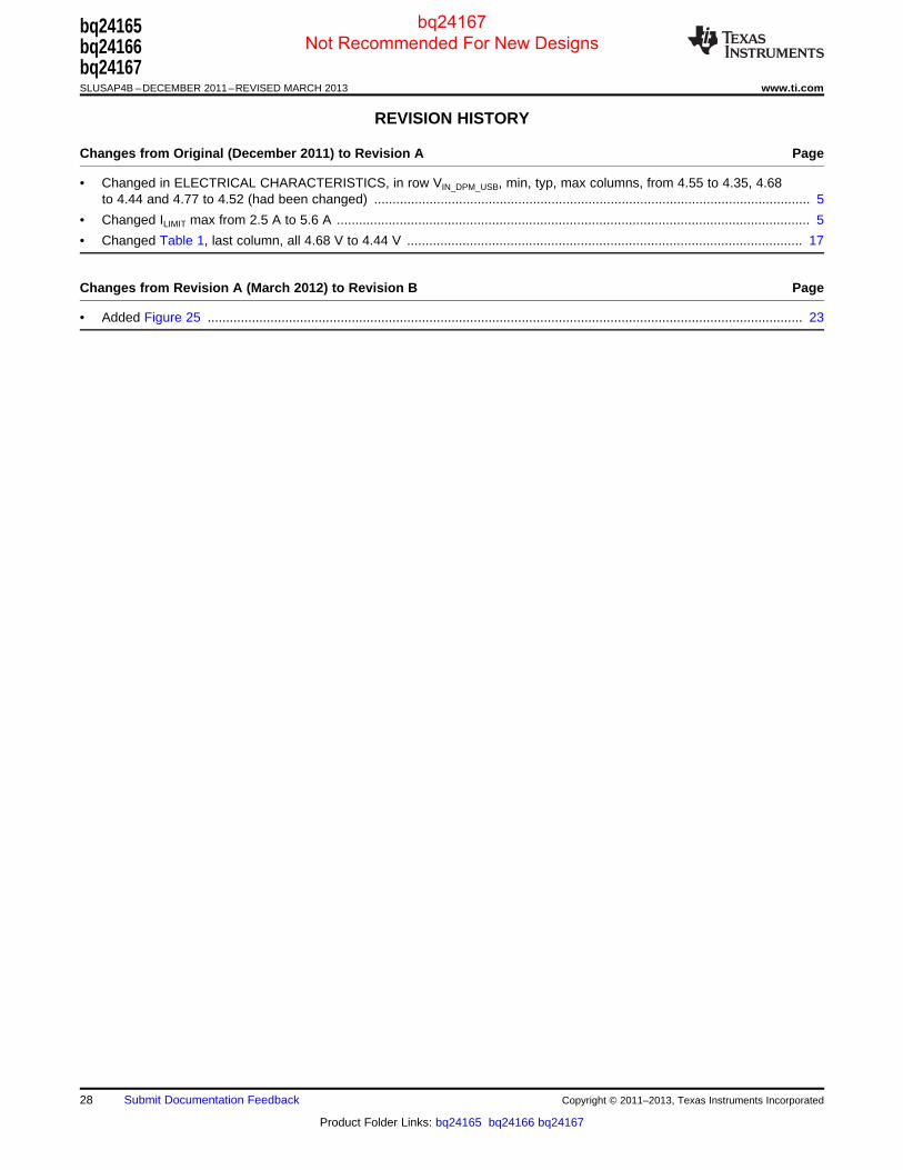
REVISION HISTORY
Changes from Original (December 2011) to Revision A Page
• Changed in ELECTRICAL CHARACTERISTICS, in row VIN_DPM_USB, min, typ, max columns, from 4.55 to 4.35, 4.68to 4.44 and 4.77 to 4.52 (had been changed) ...................................................................................................................... 5
• Changed ILIMIT max from 2.5 A to 5.6 A ................................................................................................................................ 5
• Changed Table 1, last column, all 4.68 V to 4.44 V ........................................................................................................... 17
Changes from Revision A (March 2012) to Revision B Page
• Added Figure 25 ................................................................................................................................................................. 23
28 Submit Documentation Feedback Copyright © 2011–2013, Texas Instruments Incorporated
Product Folder Links: bq24165 bq24166 bq24167
bq24167 Not Recommended For New Designs
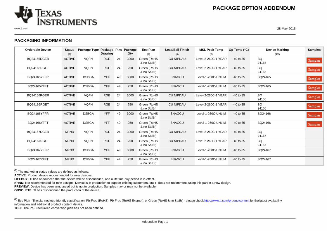
PACKAGE OPTION ADDENDUM
www.ti.com 28-May-2015
Addendum-Page 1
PACKAGING INFORMATION
Orderable Device Status(1)
Package Type PackageDrawing
Pins PackageQty
Eco Plan(2)
Lead/Ball Finish(6)
MSL Peak Temp(3)
Op Temp (°C) Device Marking(4/5)
Samples
BQ24165RGER ACTIVE VQFN RGE 24 3000 Green (RoHS& no Sb/Br)
CU NIPDAU Level-2-260C-1 YEAR -40 to 85 BQ24165
BQ24165RGET ACTIVE VQFN RGE 24 250 Green (RoHS& no Sb/Br)
CU NIPDAU Level-2-260C-1 YEAR -40 to 85 BQ24165
BQ24165YFFR ACTIVE DSBGA YFF 49 3000 Green (RoHS& no Sb/Br)
SNAGCU Level-1-260C-UNLIM -40 to 85 BQ24165
BQ24165YFFT ACTIVE DSBGA YFF 49 250 Green (RoHS& no Sb/Br)
SNAGCU Level-1-260C-UNLIM -40 to 85 BQ24165
BQ24166RGER ACTIVE VQFN RGE 24 3000 Green (RoHS& no Sb/Br)
CU NIPDAU Level-2-260C-1 YEAR -40 to 85 BQ24166
BQ24166RGET ACTIVE VQFN RGE 24 250 Green (RoHS& no Sb/Br)
CU NIPDAU Level-2-260C-1 YEAR -40 to 85 BQ24166
BQ24166YFFR ACTIVE DSBGA YFF 49 3000 Green (RoHS& no Sb/Br)
SNAGCU Level-1-260C-UNLIM -40 to 85 BQ24166
BQ24166YFFT ACTIVE DSBGA YFF 49 250 Green (RoHS& no Sb/Br)
SNAGCU Level-1-260C-UNLIM -40 to 85 BQ24166
BQ24167RGER NRND VQFN RGE 24 3000 Green (RoHS& no Sb/Br)
CU NIPDAU Level-2-260C-1 YEAR -40 to 85 BQ24167
BQ24167RGET NRND VQFN RGE 24 250 Green (RoHS& no Sb/Br)
CU NIPDAU Level-2-260C-1 YEAR -40 to 85 BQ24167
BQ24167YFFR NRND DSBGA YFF 49 3000 Green (RoHS& no Sb/Br)
SNAGCU Level-1-260C-UNLIM -40 to 85 BQ24167
BQ24167YFFT NRND DSBGA YFF 49 250 Green (RoHS& no Sb/Br)
SNAGCU Level-1-260C-UNLIM -40 to 85 BQ24167
(1) The marketing status values are defined as follows:ACTIVE: Product device recommended for new designs.LIFEBUY: TI has announced that the device will be discontinued, and a lifetime-buy period is in effect.NRND: Not recommended for new designs. Device is in production to support existing customers, but TI does not recommend using this part in a new design.PREVIEW: Device has been announced but is not in production. Samples may or may not be available.OBSOLETE: TI has discontinued the production of the device.
(2) Eco Plan - The planned eco-friendly classification: Pb-Free (RoHS), Pb-Free (RoHS Exempt), or Green (RoHS & no Sb/Br) - please check http://www.ti.com/productcontent for the latest availabilityinformation and additional product content details.TBD: The Pb-Free/Green conversion plan has not been defined.

PACKAGE OPTION ADDENDUM
www.ti.com 28-May-2015
Addendum-Page 2
Pb-Free (RoHS): TI's terms "Lead-Free" or "Pb-Free" mean semiconductor products that are compatible with the current RoHS requirements for all 6 substances, including the requirement thatlead not exceed 0.1% by weight in homogeneous materials. Where designed to be soldered at high temperatures, TI Pb-Free products are suitable for use in specified lead-free processes.Pb-Free (RoHS Exempt): This component has a RoHS exemption for either 1) lead-based flip-chip solder bumps used between the die and package, or 2) lead-based die adhesive used betweenthe die and leadframe. The component is otherwise considered Pb-Free (RoHS compatible) as defined above.Green (RoHS & no Sb/Br): TI defines "Green" to mean Pb-Free (RoHS compatible), and free of Bromine (Br) and Antimony (Sb) based flame retardants (Br or Sb do not exceed 0.1% by weightin homogeneous material)
(3) MSL, Peak Temp. - The Moisture Sensitivity Level rating according to the JEDEC industry standard classifications, and peak solder temperature.
(4) There may be additional marking, which relates to the logo, the lot trace code information, or the environmental category on the device.
(5) Multiple Device Markings will be inside parentheses. Only one Device Marking contained in parentheses and separated by a "~" will appear on a device. If a line is indented then it is a continuationof the previous line and the two combined represent the entire Device Marking for that device.
(6) Lead/Ball Finish - Orderable Devices may have multiple material finish options. Finish options are separated by a vertical ruled line. Lead/Ball Finish values may wrap to two lines if the finishvalue exceeds the maximum column width.
Important Information and Disclaimer:The information provided on this page represents TI's knowledge and belief as of the date that it is provided. TI bases its knowledge and belief on informationprovided by third parties, and makes no representation or warranty as to the accuracy of such information. Efforts are underway to better integrate information from third parties. TI has taken andcontinues to take reasonable steps to provide representative and accurate information but may not have conducted destructive testing or chemical analysis on incoming materials and chemicals.TI and TI suppliers consider certain information to be proprietary, and thus CAS numbers and other limited information may not be available for release.
In no event shall TI's liability arising out of such information exceed the total purchase price of the TI part(s) at issue in this document sold by TI to Customer on an annual basis.
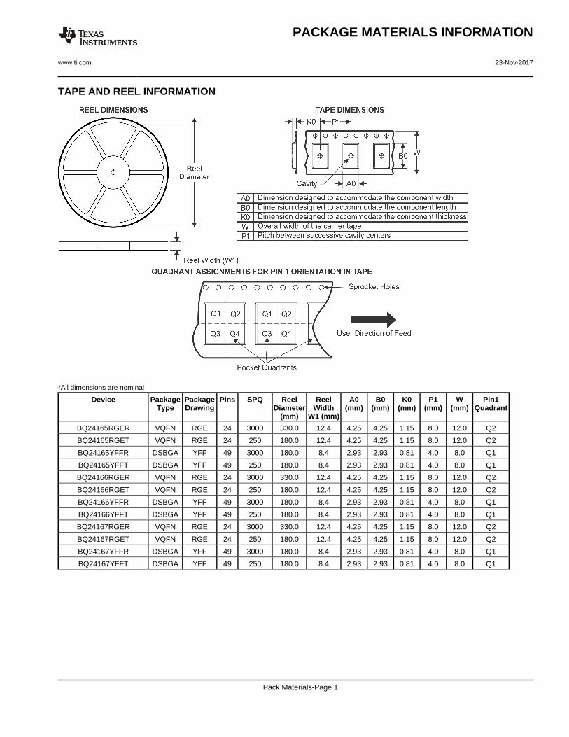
TAPE AND REEL INFORMATION
*All dimensions are nominal
Device PackageType
PackageDrawing
Pins SPQ ReelDiameter
(mm)
ReelWidth
W1 (mm)
A0(mm)
B0(mm)
K0(mm)
P1(mm)
W(mm)
Pin1Quadrant
BQ24165RGER VQFN RGE 24 3000 330.0 12.4 4.25 4.25 1.15 8.0 12.0 Q2
BQ24165RGET VQFN RGE 24 250 180.0 12.4 4.25 4.25 1.15 8.0 12.0 Q2
BQ24165YFFR DSBGA YFF 49 3000 180.0 8.4 2.93 2.93 0.81 4.0 8.0 Q1
BQ24165YFFT DSBGA YFF 49 250 180.0 8.4 2.93 2.93 0.81 4.0 8.0 Q1
BQ24166RGER VQFN RGE 24 3000 330.0 12.4 4.25 4.25 1.15 8.0 12.0 Q2
BQ24166RGET VQFN RGE 24 250 180.0 12.4 4.25 4.25 1.15 8.0 12.0 Q2
BQ24166YFFR DSBGA YFF 49 3000 180.0 8.4 2.93 2.93 0.81 4.0 8.0 Q1
BQ24166YFFT DSBGA YFF 49 250 180.0 8.4 2.93 2.93 0.81 4.0 8.0 Q1
BQ24167RGER VQFN RGE 24 3000 330.0 12.4 4.25 4.25 1.15 8.0 12.0 Q2
BQ24167RGET VQFN RGE 24 250 180.0 12.4 4.25 4.25 1.15 8.0 12.0 Q2
BQ24167YFFR DSBGA YFF 49 3000 180.0 8.4 2.93 2.93 0.81 4.0 8.0 Q1
BQ24167YFFT DSBGA YFF 49 250 180.0 8.4 2.93 2.93 0.81 4.0 8.0 Q1
PACKAGE MATERIALS INFORMATION
www.ti.com 23-Nov-2017
Pack Materials-Page 1

*All dimensions are nominal
Device Package Type Package Drawing Pins SPQ Length (mm) Width (mm) Height (mm)
BQ24165RGER VQFN RGE 24 3000 367.0 367.0 35.0
BQ24165RGET VQFN RGE 24 250 210.0 185.0 35.0
BQ24165YFFR DSBGA YFF 49 3000 182.0 182.0 20.0
BQ24165YFFT DSBGA YFF 49 250 182.0 182.0 20.0
BQ24166RGER VQFN RGE 24 3000 367.0 367.0 35.0
BQ24166RGET VQFN RGE 24 250 210.0 185.0 35.0
BQ24166YFFR DSBGA YFF 49 3000 182.0 182.0 20.0
BQ24166YFFT DSBGA YFF 49 250 182.0 182.0 20.0
BQ24167RGER VQFN RGE 24 3000 367.0 367.0 35.0
BQ24167RGET VQFN RGE 24 250 210.0 185.0 35.0
BQ24167YFFR DSBGA YFF 49 3000 182.0 182.0 20.0
BQ24167YFFT DSBGA YFF 49 250 182.0 182.0 20.0
PACKAGE MATERIALS INFORMATION
www.ti.com 23-Nov-2017
Pack Materials-Page 2

GENERIC PACKAGE VIEW
Images above are just a representation of the package family, actual package may vary.Refer to the product data sheet for package details.
RGE 24 VQFN - 1 mm max heightPLASTIC QUAD FLATPACK - NO LEAD
4204104/H

NOTES:
1. All linear dimensions are in millimeters. Any dimensions in parenthesis are for reference only. Dimensioning and tolerancing
per ASME Y14.5M.
2. This drawing is subject to change without notice.
3. The package thermal pad must be soldered to the printed circuit board for thermal and mechanical performance.
PACKAGE OUTLINE
www.ti.com
4219016 / A 08/2017
VQFN - 1 mm max height
PLASTIC QUAD FLATPACK- NO LEAD
RGE0024H
A
0.08 C
0.1 C A B
0.05 C
B
SYMM
SYMM
4.1
3.9
4.1
3.9
PIN 1 INDEX AREA
1 MAX
0.05
0.00
SEATING PLANE
C
2X 2.5
2.7±0.1
2X
2.5
20X 0.5
1
6
7
12
13
18
19
24
24X
0.30
0.18
24X
0.48
0.28
(0.2) TYP
PIN 1 ID
(OPTIONAL)
25
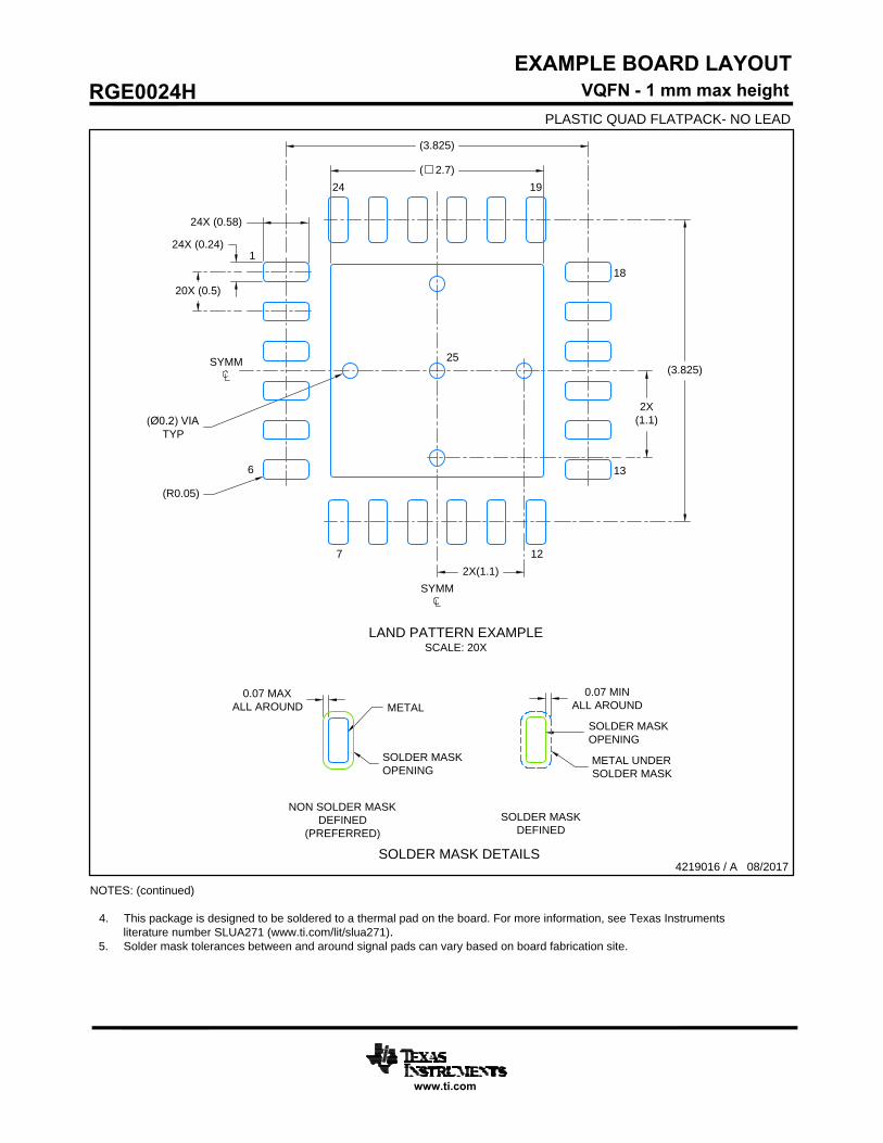
NOTES: (continued)
4. This package is designed to be soldered to a thermal pad on the board. For more information, see Texas Instruments
literature number SLUA271 (www.ti.com/lit/slua271).5. Solder mask tolerances between and around signal pads can vary based on board fabrication site.
EXAMPLE BOARD LAYOUT
4219016 / A 08/2017
www.ti.com
VQFN - 1 mm max height
RGE0024H
PLASTIC QUAD FLATPACK- NO LEAD
SYMM
SYMM
LAND PATTERN EXAMPLE
SCALE: 20X
2X
(1.1)
2X(1.1)
(3.825)
(3.825)
( 2.7)
1
6
7 12
13
18
1924
25
24X (0.58)
24X (0.24)
20X (0.5)
(R0.05)
(Ø0.2) VIA
TYP
SOLDER MASK DETAILS
NON SOLDER MASK
DEFINED
(PREFERRED)
SOLDER MASK
DEFINED
0.07 MAX
ALL AROUND
0.07 MIN
ALL AROUND
METAL
SOLDER MASK
OPENING
SOLDER MASK
OPENING
METAL UNDER
SOLDER MASK

NOTES: (continued)
6. Laser cutting apertures with trapezoidal walls and rounded corners may offer better paste release. IPC-7525 may have alternate
design recommendations..
EXAMPLE STENCIL DESIGN
4219016 / A 08/2017
www.ti.com
VQFN - 1 mm max height
RGE0024H
PLASTIC QUAD FLATPACK- NO LEAD
SYMM
SYMM
SOLDER PASTE EXAMPLE
BASED ON 0.125 mm THICK STENCIL
EXPOSED PAD
78% PRINTED COVERAGE BY AREA
SCALE: 20X
(3.825)
(3.825)
(0.694)
TYP
(0.694)
TYP
4X ( 1.188)
1
6
712
13
18
1924
24X (0.24)
24X (0.58)
20X (0.5)
(R0.05) TYP
METAL
TYP
25

IMPORTANT NOTICE
Texas Instruments Incorporated (TI) reserves the right to make corrections, enhancements, improvements and other changes to itssemiconductor products and services per JESD46, latest issue, and to discontinue any product or service per JESD48, latest issue. Buyersshould obtain the latest relevant information before placing orders and should verify that such information is current and complete.TI’s published terms of sale for semiconductor products (http://www.ti.com/sc/docs/stdterms.htm) apply to the sale of packaged integratedcircuit products that TI has qualified and released to market. Additional terms may apply to the use or sale of other types of TI products andservices.Reproduction of significant portions of TI information in TI data sheets is permissible only if reproduction is without alteration and isaccompanied by all associated warranties, conditions, limitations, and notices. TI is not responsible or liable for such reproduceddocumentation. Information of third parties may be subject to additional restrictions. Resale of TI products or services with statementsdifferent from or beyond the parameters stated by TI for that product or service voids all express and any implied warranties for theassociated TI product or service and is an unfair and deceptive business practice. TI is not responsible or liable for any such statements.Buyers and others who are developing systems that incorporate TI products (collectively, “Designers”) understand and agree that Designersremain responsible for using their independent analysis, evaluation and judgment in designing their applications and that Designers havefull and exclusive responsibility to assure the safety of Designers' applications and compliance of their applications (and of all TI productsused in or for Designers’ applications) with all applicable regulations, laws and other applicable requirements. Designer represents that, withrespect to their applications, Designer has all the necessary expertise to create and implement safeguards that (1) anticipate dangerousconsequences of failures, (2) monitor failures and their consequences, and (3) lessen the likelihood of failures that might cause harm andtake appropriate actions. Designer agrees that prior to using or distributing any applications that include TI products, Designer willthoroughly test such applications and the functionality of such TI products as used in such applications.TI’s provision of technical, application or other design advice, quality characterization, reliability data or other services or information,including, but not limited to, reference designs and materials relating to evaluation modules, (collectively, “TI Resources”) are intended toassist designers who are developing applications that incorporate TI products; by downloading, accessing or using TI Resources in anyway, Designer (individually or, if Designer is acting on behalf of a company, Designer’s company) agrees to use any particular TI Resourcesolely for this purpose and subject to the terms of this Notice.TI’s provision of TI Resources does not expand or otherwise alter TI’s applicable published warranties or warranty disclaimers for TIproducts, and no additional obligations or liabilities arise from TI providing such TI Resources. TI reserves the right to make corrections,enhancements, improvements and other changes to its TI Resources. TI has not conducted any testing other than that specificallydescribed in the published documentation for a particular TI Resource.Designer is authorized to use, copy and modify any individual TI Resource only in connection with the development of applications thatinclude the TI product(s) identified in such TI Resource. NO OTHER LICENSE, EXPRESS OR IMPLIED, BY ESTOPPEL OR OTHERWISETO ANY OTHER TI INTELLECTUAL PROPERTY RIGHT, AND NO LICENSE TO ANY TECHNOLOGY OR INTELLECTUAL PROPERTYRIGHT OF TI OR ANY THIRD PARTY IS GRANTED HEREIN, including but not limited to any patent right, copyright, mask work right, orother intellectual property right relating to any combination, machine, or process in which TI products or services are used. Informationregarding or referencing third-party products or services does not constitute a license to use such products or services, or a warranty orendorsement thereof. Use of TI Resources may require a license from a third party under the patents or other intellectual property of thethird party, or a license from TI under the patents or other intellectual property of TI.TI RESOURCES ARE PROVIDED “AS IS” AND WITH ALL FAULTS. TI DISCLAIMS ALL OTHER WARRANTIES ORREPRESENTATIONS, EXPRESS OR IMPLIED, REGARDING RESOURCES OR USE THEREOF, INCLUDING BUT NOT LIMITED TOACCURACY OR COMPLETENESS, TITLE, ANY EPIDEMIC FAILURE WARRANTY AND ANY IMPLIED WARRANTIES OFMERCHANTABILITY, FITNESS FOR A PARTICULAR PURPOSE, AND NON-INFRINGEMENT OF ANY THIRD PARTY INTELLECTUALPROPERTY RIGHTS. TI SHALL NOT BE LIABLE FOR AND SHALL NOT DEFEND OR INDEMNIFY DESIGNER AGAINST ANY CLAIM,INCLUDING BUT NOT LIMITED TO ANY INFRINGEMENT CLAIM THAT RELATES TO OR IS BASED ON ANY COMBINATION OFPRODUCTS EVEN IF DESCRIBED IN TI RESOURCES OR OTHERWISE. IN NO EVENT SHALL TI BE LIABLE FOR ANY ACTUAL,DIRECT, SPECIAL, COLLATERAL, INDIRECT, PUNITIVE, INCIDENTAL, CONSEQUENTIAL OR EXEMPLARY DAMAGES INCONNECTION WITH OR ARISING OUT OF TI RESOURCES OR USE THEREOF, AND REGARDLESS OF WHETHER TI HAS BEENADVISED OF THE POSSIBILITY OF SUCH DAMAGES.Unless TI has explicitly designated an individual product as meeting the requirements of a particular industry standard (e.g., ISO/TS 16949and ISO 26262), TI is not responsible for any failure to meet such industry standard requirements.Where TI specifically promotes products as facilitating functional safety or as compliant with industry functional safety standards, suchproducts are intended to help enable customers to design and create their own applications that meet applicable functional safety standardsand requirements. Using products in an application does not by itself establish any safety features in the application. Designers mustensure compliance with safety-related requirements and standards applicable to their applications. Designer may not use any TI products inlife-critical medical equipment unless authorized officers of the parties have executed a special contract specifically governing such use.Life-critical medical equipment is medical equipment where failure of such equipment would cause serious bodily injury or death (e.g., lifesupport, pacemakers, defibrillators, heart pumps, neurostimulators, and implantables). Such equipment includes, without limitation, allmedical devices identified by the U.S. Food and Drug Administration as Class III devices and equivalent classifications outside the U.S.TI may expressly designate certain products as completing a particular qualification (e.g., Q100, Military Grade, or Enhanced Product).Designers agree that it has the necessary expertise to select the product with the appropriate qualification designation for their applicationsand that proper product selection is at Designers’ own risk. Designers are solely responsible for compliance with all legal and regulatoryrequirements in connection with such selection.Designer will fully indemnify TI and its representatives against any damages, costs, losses, and/or liabilities arising out of Designer’s non-compliance with the terms and provisions of this Notice.
Mailing Address: Texas Instruments, Post Office Box 655303, Dallas, Texas 75265Copyright © 2018, Texas Instruments Incorporated