25q40 4 megabit serial flash memory with 4kbytes uniform...
TRANSCRIPT
25Q40
Zetta Confidential Version A 1
4 Megabit Serial Flash Memory with 4Kbytes Uniform Sector ZD25Q40
FEATURES Family of SPI Flash Memories Flexible Architecture with 4KB sectors
- ZD25Q: 4M-bit / 512K-byte - Standard SPI: CLK, /CS, DI, DO, /WP, /Hold - Dual SPI: CLK, /CS, IO0, IO1, /WP, /Hold - Quad SPI: CLK, /CS, IO0, IO1, IO2, IO3
- Uniform Sector Erase (4K-bytes) - Uniform Block Erase (32K and 64K-bytes) - Program 1 to 256 byte per programmable page
Highest Performance Serial Flash Advanced Security Features - 108MHz Standard/Dual/Quad SPI clocks - More than 100,000 erase/program cycles - More than 20-year data retention - Continuous Read With 8/16/32/64-byte Wrap
- Write protect all/portion of memory via software - Enable/Disable protection with WP# Pin
Low Power consumption Space Efficien Packaging
- 8 mA typical active current - 10mA active current, <1µA Power-down (typ.)
- 8-pin SOIC 208/150-mil - 8-pad USON 2x3-mm - TSSOP8 (173mil) - Contact Zetta for KGD and other options
GENERAL DESCRIPTION
The ZD25Q40 (4M-bit) Serial Flash memory provides a storage solution for systems with limited space, pins and power. The ZD25Q40 series offers flexibility and performance well beyond ordinary Serial Flash devices. They are ideal for code shadowing to RAM, executing code directly from Dual/Quad SPI (XIP) and storing voice, text and data. The device operates on a single 2.7V to 3.6V power supply with current consumption as low as 10mA active and 1µA for power-down. All devices are offered in space- saving packages.
The ZD25Q40 support the standard Serial Peripheral Interface (SPI), as well as Dual/Quad I/O SPI: Serial Clock, Chip Select, Serial Data I/O0 (DI), I/O1 (DO), I/O2 (/WP), and I/O3 (/HOLD). SPI clock frequencies of up to 108MHz are supported allowing equivalent clock rates of 216MHz (108MHz x 2) for Dual I/O and 432MHz (108MHz x 4) for Quad I/O when using the Fast Read Dual/Quad I/O instructions. These transfer rates can outperform standard Asynchronous 8 and 16-bit Parallel Flash memories.
A Hold pin, Write Protect pin and programmable write protection, with top or bottom array control, provide further control flexibility.

25Q40
Zetta Confidential Version A 2
1. ORDERING INFORMATION
Package Type S: 208mil SOP8 T: 150mil SOP8 U: USON8 (3*2mm) E: USON8 (3*3mm, 0.65mm) N: USON8(3*3mm, 0.5mm) O: 173mil TSSOP8
ZD25Q XX X X X X X
Temperature Range I: Industriial(-40℃~85℃) A: Automotive (-40 ~12℃ 5 )℃
Base Part Number ZD: Zetta 25Q:3V Serial 4Kbyte Uniform-sector Flash
VersionA: A Version B: B Version C: C Version
Packaging Type T:Tube R:Tape & Reel Y:Tray
Figure 1, Ordering Information
Device Density 20: 2Mbit 40: 4Mbit 80: 8Mbit 16: 16Mbit
Green Code G: Low-halogen, Lead(Pb)-free P: Lead (Pb) - free
25Q40
Zetta Confidential Version A 3
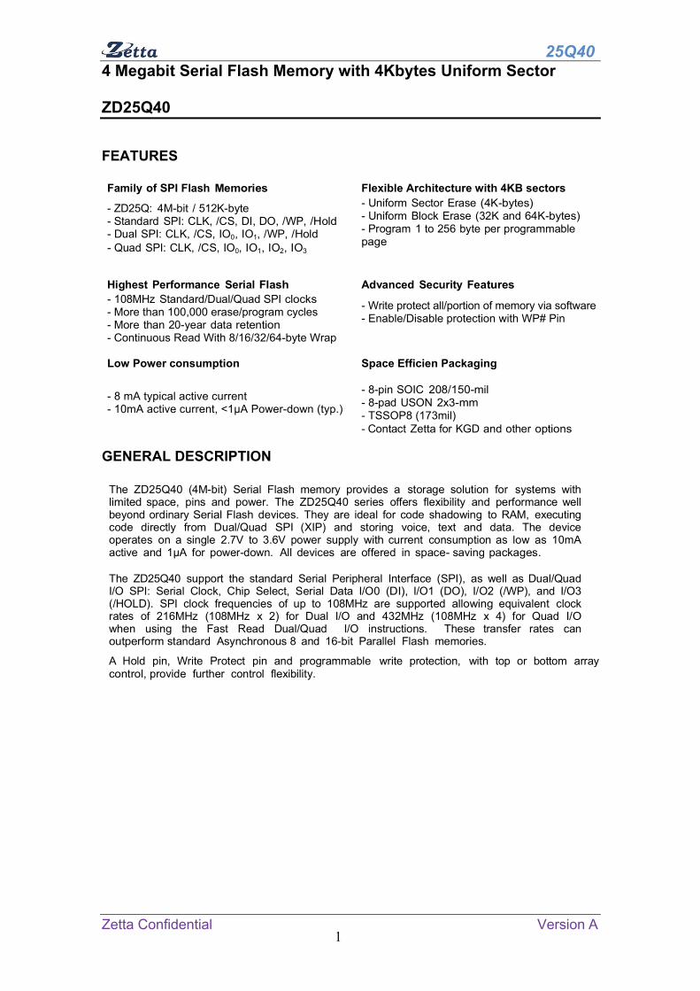
2. BLOCK DIAGRAM
Figure 2, Block Diagram
25Q40
Zetta Confidential Version A 4
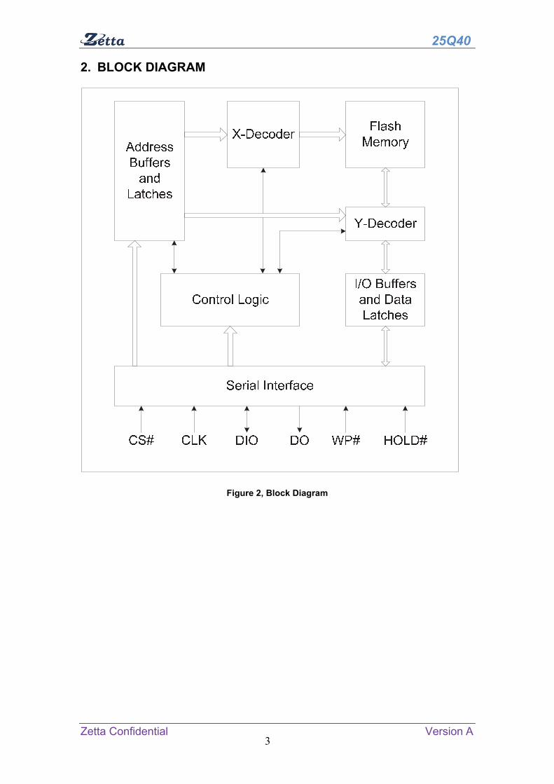
3. CONNECTION DIAGRAMS
Figure 3.1, 8–LEAD SOP/VSOP/DIP Figure 3.2, 8-Contact 6 x 5 mm WSON

25Q40
Zetta Confidential Version A 5
4. SIGNAL DESCRIPTIONS Serial Data Input, Output and IOs (DI, DO and IO0, IO1, IO2, IO3) The ZD25Q40 supports standard SPI, Dual SPI and Quad SPI operation. Standard SPI instructions use the unidirectional DI (input) pin to serially write instructions, addresses or data to the device on the rising edge of the Serial Clock (CLK) input pin. Standard SPI also uses the unidirectional DO (output) to read data or status from the device on the falling edge of CLK. Dual/Quad SPI instructions use the bidirectional IO pins to serially write instructions, addresses or data to the device on the rising edge of CLK and read data or status from the device on the falling edge of CLK. When use Quad Output instructions, the /WP pin becomes IO2 and /HOLD pin becomes IO3. Serial Clock (CLK) The SPI Serial Clock Input (CLK) pin provides the timing for serial input and output operations. ("See SPI Mode") Chip Select (CS#) The SPI Chip Select (/CS) pin enables and disables device operation. When /CS is high, the device is deselected and the Serial Data Output (DO, or IO0, IO1, IO2, IO3) pins are at high impedance. When deselected, the devices power consumption will be at standby levels unless an internal erase, program or write status register cycle is in progress. When /CS is brought low, the device will be selected, power consumption will increase to active levels and instructions can be written to and data read from the device. After power-up, /CS must transition from high to low before a new instruction will be accepted. The /CS input must track the VCC supply level at power-up and power-down. If needed a pull-up resister on /CS can be used to accomplish this. Write Protect (WP#) The Write Protect (/WP) pin can be used to prevent the Status Registers from being written. Used in Conjunction with the Status Register’s Block Protect (CMP, SEC, TB, BP2, BP1 and BP0) bits and Status Register Protect (SRP) bits, a portion as small as a 4KB sector or the entire memory array can be hardware protected. The /WP pin is active low.
Table1, Pin Descriptions
*1 IO0 and IO1 are used for Standard and Dual SPI instructions *2 IO3 are used for Quad SPI instructions
Symbol Pin Name
/CS Chip Select Input
DO (IO1) Data Output (Data Input Output 1)*1
/WP (IO2) Write Protect Input ( Data Input Output 2)*2
GND Ground
DI (IO0) Data Input (Data Input Output 0)*1
CLK Serial Clock Input
/HOLD (IO3) Hold Input (Data Input Output 3)*2

25Q40
Zetta Confidential Version A 6
5. MEMORY ORGANIZATIONS The memory is organized as: - 524,288bytes - Uniform Sector Architecture 8 blocks of 64-Kbyte 128 sectors of 4-Kbyte 2,048 pages (256 bytes each)
Each page can be individually programmed (bits are programmed from 1 to 0). The device is Sector, Block or Chip Erasable but not Page Erasable.
xxFF00h xxFFFFh 7FF00h 7FFFFh
. . . .xxF000h xxF0FFh 70000h 700FFh
xxEF00h xxEFFFh
. .xxE000h xxE0FFh
04FF00h 04FFFFh
. .040000h 0400FFh
03FF00h 03FFFFh
. .030000h 0300FFh
xx1F00h xx1FFFh
. .xx1000h xx10FFh
xx0F00h xx0FFFh 00FF00h 00FFFFh
. . . .xx0000h xx00FFh 000000h 0000FFh
...
…
...
Sector 15(4KB) Block 7(64KB)
Sector 14(4KB)
Sector 0(4KB)
Sector 1(4KB)
Block 3(64KB)
Block 4(64KB)
Block 0(64KB)
Figure 4, Memory Organization

25Q40
Zetta Confidential Version A 7
6. FUNCTION DESCRIPTION Standard SPI Instructions
The ZD25Q40 is accessed through an SPI compatible bus consisting of four signals: Serial Clock (CLK), Chip Select (/CS), Serial Data Input (DI) and Serial Data Output (DO). Standard SPI instructions use the DI input pin to serially write instructions, addresses or data to the device on the rising edge of CLK. The DO output pin is used to read data or status from the device on the falling edge of CLK. SPI bus operation Mode 0 (0,0) and 3 (1,1) are supported. The primary difference between Mode 0 and Mode 3 concerns the normal state of the CLK signal when the SPI bus master is in standby and data is not being transferred to the Serial Flash. For Mode 0, the CLK signal is normally low on the falling and rising edges of /CS. For Mode 3, the CLK signal is normally high on the falling and rising edges of /CS.
Figure 5, SPI Modes Dual SPI The ZD25Q40 supports Dual SPI operation when using the “Dual Output Fast Read” (3BH) and “Dual I/O Fast Read” (BBH) commands. These commands allow data to be transferred to or from the device at two times the rate of the standard SPI. When using the Dual SPI command the SI and SO pins become bidirectional I/O pins: IO0 and IO1. Quad SPI The ZD25Q40 supports Quad SPI operation when using the “Quad Output Fast Read”(6BH),”Quad I/O Fast Read”(EBH), “Quad I/O Word Fast Read”(E7H) and “Quad Page Program” (32H) commands. These commands allow data to be transferred to or from the device at four times the rate of the standard SPI. When using the Quad SPI command the SI and SO pins become bidirectional I/O pins: IO0 and IO1, and WP# and HOLD# pins become IO2 and IO3. Quad SPI commands require the non-volatile Quad Enable bit (QE) in Status Register to be set. Hold The HOLD# function is only available when QE=0, If QE=1, The HOLD# functions is disabled, the pin acts as dedicated data I/O pin. The HOLD# signal goes low to stop any serial communications with the device, but doesn’t stop the operation of write status register, programming, or erasing in progress. The operation of HOLD, need CS# keep low, and starts on falling edge of the HOLD# signal, with SCLK signal being low (if SCLK is not being low, HOLD operation will not start until SCLK being low). The HOLD condition ends on rising edge of HOLD# signal with SCLK being low (If SCLK is not being low, HOLD operation will not end until SCLK being low). The SO is high impedance, both SI and SCLK don’t care during the HOLD operation, if CS# drives high during HOLD operation, it will reset the internal logic of the device. To re-start communication with chip, the HOLD# must be at high and then CS# must be at low.
25Q40
Zetta Confidential Version A 8
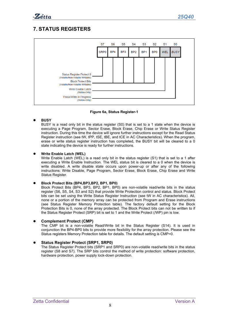
7. STATUS REGISTERS
Figure 6a, Status Register-1 BUSY
BUSY is a read only bit in the status register (S0) that is set to a 1 state when the device is executing a Page Program, Sector Erase, Block Erase, Chip Erase or Write Status Register instruction. During this time the device will ignore further instructions except for the Read Status Register instruction (see tW, tPP, tSE, tBE, and tCE in AC Characteristics). When the program, erase or write status register instruction has completed, the BUSY bit will be cleared to a 0 state indicating the device is ready for further instructions.
Write Enable Latch (WEL) Write Enable Latch (WEL) is a read only bit in the status register (S1) that is set to a 1 after executing a Write Enable Instruction. The WEL status bit is cleared to a 0 when the device is write disabled. A write disable state occurs upon power-up or after any of the following instructions: Write Disable, Page Program, Sector Erase, Block Erase, Chip Erase and Write Status Register.
Block Protect Bits (BP4,BP3,BP2, BP1, BP0)
Block Protect Bits (BP4, BP3, BP2, BP1, BP0) are non-volatile read/write bits in the status register (S6, S5, S4, S3 and S2) that provide Write Protection control and status. Block Protect bits can be set using the Write Status Register Instruction (see tW in AC characteristics). All, none or a portion of the memory array can be protected from Program and Erase instructions (see Status Register Memory Protection table). The factory default setting for the Block Protection Bits is 0, none of the array protected. The Block Protect bits can not be written to if the Status Register Protect (SRP) bit is set to 1 and the Write Protect (/WP) pin is low.
Complement Protect (CMP)
The CMP bit is a non-volatile Read/Write bit in the Status Register (S14). It is used in conjunction the BP4-BP0 bits to provide more flexibility for the array protection. Please see the Status registers Memory Protection table for details. The default setting is CMP=0.
Status Register Protect (SRP1, SRP0)
The Status Register Protect bits (SRP1 and SRP0) are non-volatile read/write bits in the status register (S8 and S7). The SRP bits control the method of write protection: software protection, hardware protection, power supply lock-down protection.

25Q40
Zetta Confidential Version A 9
Figure 6b, Status Register-2
Quad Enable (QE) The Quad Enable (QE) bit is a non-volatile read/write bit in the status register (S9) that allows Quad SPI operation. When the QE bit is set to a 0 state, the /WP pin and /HOLD are enabled. When the QE bit is set to a 1, the Quad IO2 and IO3 pins are enabled, and /WP and /HOLD functions are disabled. WARNING: If the /WP or /HOLD pins are tied directly to the power supply or ground during standard SPI or Dual SPI operation, the QE bit should never be set to a 1.
Reserved Bits There are a few reserved Status Register bits that may be read out as a “0” or “1”. It is recommended to ignore the values of those bits. During a “Write Status Register” instruction, the Reserved Bits can be written as “0”, but there will not be any effects.
25Q40
Zetta Confidential Version A 10
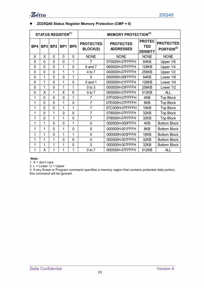
ZD25Q40 Status Register Memory Protection (CMP = 0)
BP4 BP3 BP2 BP1 BP0PROTECTED
BLOCK(S)PROTECTEDADDRESSES
PROTECTED
DENSITY
PROTECTED
PORTION(2)
X X 0 0 0 NONE NONE NONE NONE0 0 0 0 1 7 070000H-07FFFFH 64KB Upper 1/80 0 0 1 0 6 and 7 060000H-07FFFFH 128KB Upper 1/40 0 0 1 1 4 to 7 040000H-07FFFFH 256KB Upper 1/20 1 0 0 1 0 000000H-00FFFFH 64KB Lower 1/80 1 0 1 0 0 and 1 000000H-01FFFFH 128KB Lower 1/40 1 0 1 1 0 to 3 000000H-03FFFFH 256KB Lower 1/20 X 1 X X 0 to 7 000000H-07FFFFH 512KB ALL1 0 0 0 1 7 07F000H-07FFFFH 4KB Top Block1 0 0 1 0 7 07E000H-07FFFFH 8KB Top Block1 0 0 1 1 7 07C000H-07FFFFH 16KB Top Block1 0 1 0 X 7 078000H-07FFFFH 32KB Top Block1 0 1 1 0 7 078000H-07FFFFH 32KB Top Block1 1 0 0 1 0 000000H-000FFFH 4KB Bottom Block
1 1 0 1 0 0 000000H-001FFFH 8KB Bottom Block
1 1 0 1 1 0 000000H-003FFFH 16KB Bottom Block1 1 1 0 X 0 000000H-007FFFH 32KB Bottom Block1 1 1 1 0 0 000000H-007FFFH 32KB Bottom Block1 X 1 1 1 0 to 7 000000H-07FFFFH 512KB ALL
STATUS REGISTER(1) MEMORY PROTECTION(3)
Note: 1. X = don’t care 2. L = Lower; U = Upper 3. If any Erase or Program command specifies a memory region that contains protected data portion, this command will be ignored.

25Q40
Zetta Confidential Version A 11
ZD25Q40 Status Register Memory Protection (CMP = 1)
BP4 BP3 BP2 BP1 BP0PROTECTED
BLOCK(S)PROTECTEDADDRESSES
PROTECTED
DENSITY
PROTECTED
PORTION(2)
X X 0 0 0 0 to 7 000000H-07FFFFH 512KB ALL0 0 0 0 1 0 to 6 000000H-06FFFFH 448KB Lower 7/80 0 0 1 0 0 to 5 000000H-05FFFFH 384KB Lower 3/40 0 0 1 1 0 to 3 000000H-03FFFFH 256KB Lower 1/20 1 0 0 1 1 to 7 010000H-07FFFFH 448KB Upper 7/80 1 0 1 0 2 to 7 020000H-07FFFFH 384KB Upper 3/40 1 0 1 1 4 to 7 040000H-07FFFFH 256KB Upper 1/20 X 1 X X NONE NONE NONE NONE1 0 0 0 1 0 to 7 000000H-07EFFFH 508KB Lower 127/1281 0 0 1 0 0 to 7 000000H-07DFFFH 504KB Lower 63/641 0 0 1 1 0 to 7 000000H-07BFFFH 496KB Lower 31/321 0 1 0 X 0 to 7 000000H-077FFFH 480KB Lower 15/161 0 1 1 0 0 to 7 000000H-077FFFH 480KB Lower 15/161 1 0 0 1 0 to 7 001000H-07FFFFH 508KB Upper 127/128
1 1 0 1 0 0 to 7 002000H-07FFFFH 504KB Upper 63/64
1 1 0 1 1 0 to 7 004000H-07FFFFH 496KB Upper 31/321 1 1 0 X 0 to 7 008000H-07FFFFH 480KB Upper 15/161 1 1 1 0 0 to 7 008000H-07FFFFH 480KB Upper 15/161 X 1 1 1 NONE NONE NONE NONE
STATUS REGISTER(1) MEMORY PROTECTION(3)
Note: 1. X = don’t care 2. L = Lower; U = Upper 3. If any Erase or Program command specifies a memory region that contains protected data portion, this command will be ignored.
25Q40
Zetta Confidential Version A 12
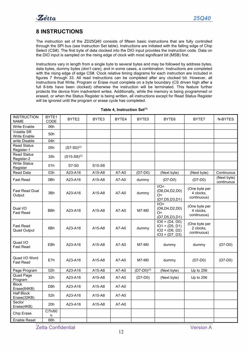
8 INSTRUCTIONS The instruction set of the ZD25Q40 consists of fifteen basic instructions that are fully controlled through the SPI bus (see Instruction Set table). Instructions are initiated with the falling edge of Chip Select (CS#). The first byte of data clocked into the DIO input provides the instruction code. Data on the DIO input is sampled on the rising edge of clock with most significant bit (MSB) first. Instructions vary in length from a single byte to several bytes and may be followed by address bytes, data bytes, dummy bytes (don’t care), and in some cases, a combination. Instructions are completed with the rising edge of edge CS#. Clock relative timing diagrams for each instruction are included in figures 7 through 33. All read instructions can be completed after any clocked bit. However, all instructions that Write, Program or Erase must complete on a byte boundary (CS driven high after a full 8-bits have been clocked) otherwise the instruction will be terminated. This feature further protects the device from inadvertent writes. Additionally, while the memory is being programmed or erased, or when the Status Register is being written, all instructions except for Read Status Register will be ignored until the program or erase cycle has completed.
Table 4, Instruction Set(1)
INSTRUCTION NAME
BYTE1 CODE
BYTE2 BYTE3 BYTE4 BYTE5 BYTE6 BYTE7 N-BYTES
Write Enable 06h
Volatile SR Write Enable
50h
write Disable 04h Read Status Register-1
05h (S7-S0)(2)
Read Status Register-2
35h (S15-S8)(2)
Write Status Register
01h S7-S0 S15-S8
Read Data 03h A23-A16 A15-A8 A7-A0 (D7-D0) (Next byte) (Next byte) Continuous
Fast Read 0Bh A23-A16 A15-A8 A7-A0 dummy (D7-D0) (D7-D0) (Next byte) continuous
Fast Read Dual Output
3Bh A23-A16 A15-A8 A7-A0 dummy
I/O= (D6,D4,D2,D0) O= (D7,D5,D3,D1)
(One byte per 4 clocks,
continuous)
Dual I/O Fast Read
BBh A23-A16 A15-A8 A7-A0 M7-M0
I/O= (D6,D4,D2,D0) O= (D7,D5,D3,D1)
(One byte per 4 clocks,
continuous)
Fast Read Quad Output
6Bh A23-A16 A15-A8 A7-A0 dummy
IO0 = (D4, D0) IO1 = (D5, D1) IO2 = (D6, D2) IO3 = (D7, D3)
(One byte per 2 clocks,
continuous)
Quad I/O Fast Read
EBh A23-A16 A15-A8 A7-A0 M7-M0 dummy dummy (D7-D0)
Quad I/O Word Fast Read
E7h A23-A16 A15-A8 A7-A0 M7-M0 dummy (D7-D0) (D7-D0)
Page Program 02h A23-A16 A15-A8 A7-A0 (D7-D0)(3) (Next byte) Up to 256 Quad Page Program
32h A23-A16 A15-A8 A7-A0 (D7-D0) (Next byte) Up to 256
Block Erase(64KB)
D8h A23-A16 A15-A8 A7-A0
Half Block Erase(32KB)
52h A23-A16 A15-A8 A7-A0
Sector Erase(4KB)
20h A23-A16 A15-A8 A7-A0
Chip Erase C7h/60
h
Enable Reset 66h
25Q40
Zetta Confidential Version A 13
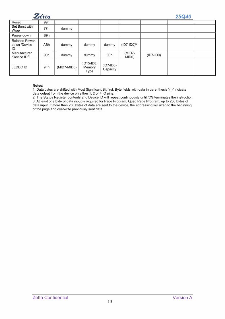
Notes: 1. Data bytes are shifted with Most Significant Bit first. Byte fields with data in parenthesis “( )” indicate data output from the device on either 1, 2 or 4 IO pins. 2. The Status Register contents and Device ID will repeat continuously until /CS terminates the instruction. 3. At least one byte of data input is required for Page Program, Quad Page Program, up to 256 bytes of data input. If more than 256 bytes of data are sent to the device, the addressing will wrap to the beginning of the page and overwrite previously sent data.
Reset 99h Set Burst with Wrap
77h dummy
Power-down B9h
Release Power-down /Device ID
ABh dummy dummy dummy (ID7-ID0)(2)
Manufacturer /Device ID(3)
90h dummy dummy 00h (MID7-MID0)
(ID7-ID0)
JEDEC ID 9Fh (MID7-MID0) (ID15-ID8) Memory
Type
(ID7-ID0) Capacity

25Q40
Zetta Confidential Version A 14
Table 5, Manufacturer and Device Identification
OP Code (MID7-MID0) (ID15-ID0) (ID7-ID0)
ABh 12h
90h BA 12h
9Fh BA 4013h
8.1 Write Enable (06h) The Write Enable instruction (Figure 7) sets the Write Enable Latch (WEL) bit in the Status Register to a 1. The WEL bit must be set prior to every Page Program, Sector Erase, Block Erase, Chip Erase and Write Status Register instruction. The Write Enable instruction is entered by driving CS# low, shifting the instruction code “06h” into the Data Input (DI) pin on the rising edge of CLK, and then driving CS# high.
CS#
CLK0 5431 2 76
Mode0 Mode0
Mode3 Mode3
DIO
DO High Impedance
Instruction(06H)
Figure 7, Write Enable Instruction Sequence Diagram
8.2 Write Disable (04h) The Write Disable instruction (Figure 8) resets the Write Enable Latch (WEL) bit in the Status Register to a 0. The Write Disable instruction is entered by driving CS# low, shifting the instruction code “04h” into the DIO pin and then driving CS# high. Note that the WEL bit is automatically reset after Power-up and upon completion of the Write Status Register, Page Program, Sector Erase, Block Erase and Chip Erase instructions.
CS#
CLK0 5431 2 76
Mode0 Mode0
Mode3 Mode3
DIO
DO High Impedance
Instruction(04H)
Figure 8, Write Disable Instruction Sequence Diagram
25Q40
Zetta Confidential Version A 15
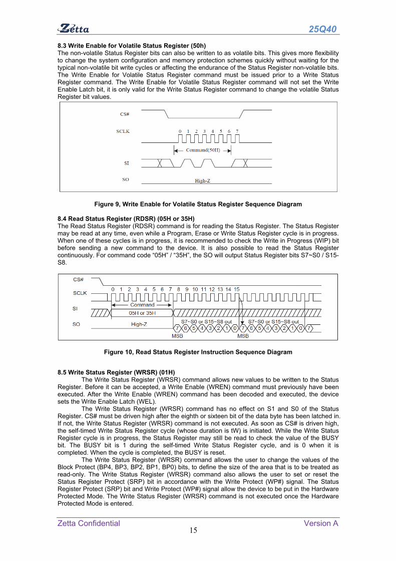
8.3 Write Enable for Volatile Status Register (50h) The non-volatile Status Register bits can also be written to as volatile bits. This gives more flexibility to change the system configuration and memory protection schemes quickly without waiting for the typical non-volatile bit write cycles or affecting the endurance of the Status Register non-volatile bits. The Write Enable for Volatile Status Register command must be issued prior to a Write Status Register command. The Write Enable for Volatile Status Register command will not set the Write Enable Latch bit, it is only valid for the Write Status Register command to change the volatile Status Register bit values.
Figure 9, Write Enable for Volatile Status Register Sequence Diagram 8.4 Read Status Register (RDSR) (05H or 35H) The Read Status Register (RDSR) command is for reading the Status Register. The Status Register may be read at any time, even while a Program, Erase or Write Status Register cycle is in progress. When one of these cycles is in progress, it is recommended to check the Write in Progress (WIP) bit before sending a new command to the device. It is also possible to read the Status Register continuously. For command code “05H” / “35H”, the SO will output Status Register bits S7~S0 / S15-S8.
Figure 10, Read Status Register Instruction Sequence Diagram
8.5 Write Status Register (WRSR) (01H) The Write Status Register (WRSR) command allows new values to be written to the Status
Register. Before it can be accepted, a Write Enable (WREN) command must previously have been executed. After the Write Enable (WREN) command has been decoded and executed, the device sets the Write Enable Latch (WEL).
The Write Status Register (WRSR) command has no effect on S1 and S0 of the Status Register. CS# must be driven high after the eighth or sixteen bit of the data byte has been latched in. If not, the Write Status Register (WRSR) command is not executed. As soon as CS# is driven high, the self-timed Write Status Register cycle (whose duration is tW) is initiated. While the Write Status Register cycle is in progress, the Status Register may still be read to check the value of the BUSY bit. The BUSY bit is 1 during the self-timed Write Status Register cycle, and is 0 when it is completed. When the cycle is completed, the BUSY is reset.
The Write Status Register (WRSR) command allows the user to change the values of the Block Protect (BP4, BP3, BP2, BP1, BP0) bits, to define the size of the area that is to be treated as read-only. The Write Status Register (WRSR) command also allows the user to set or reset the Status Register Protect (SRP) bit in accordance with the Write Protect (WP#) signal. The Status Register Protect (SRP) bit and Write Protect (WP#) signal allow the device to be put in the Hardware Protected Mode. The Write Status Register (WRSR) command is not executed once the Hardware Protected Mode is entered.
25Q40
Zetta Confidential Version A 16
Figure 11, Write Status Register Instruction Sequence Diagram
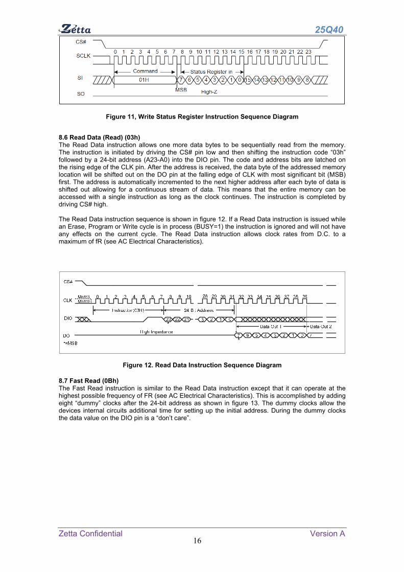
8.6 Read Data (Read) (03h) The Read Data instruction allows one more data bytes to be sequentially read from the memory. The instruction is initiated by driving the CS# pin low and then shifting the instruction code “03h” followed by a 24-bit address (A23-A0) into the DIO pin. The code and address bits are latched on the rising edge of the CLK pin. After the address is received, the data byte of the addressed memory location will be shifted out on the DO pin at the falling edge of CLK with most significant bit (MSB) first. The address is automatically incremented to the next higher address after each byte of data is shifted out allowing for a continuous stream of data. This means that the entire memory can be accessed with a single instruction as long as the clock continues. The instruction is completed by driving CS# high. The Read Data instruction sequence is shown in figure 12. If a Read Data instruction is issued while an Erase, Program or Write cycle is in process (BUSY=1) the instruction is ignored and will not have any effects on the current cycle. The Read Data instruction allows clock rates from D.C. to a maximum of fR (see AC Electrical Characteristics).
Figure 12. Read Data Instruction Sequence Diagram 8.7 Fast Read (0Bh) The Fast Read instruction is similar to the Read Data instruction except that it can operate at the highest possible frequency of FR (see AC Electrical Characteristics). This is accomplished by adding eight “dummy” clocks after the 24-bit address as shown in figure 13. The dummy clocks allow the devices internal circuits additional time for setting up the initial address. During the dummy clocks the data value on the DIO pin is a “don’t care”.

25Q40
Zetta Confidential Version A 17
Figure 13, Fast Read Instruction Sequence Diagram 8.8 Fast Read Dual Output (3Bh) The Fast Read Dual Output (3Bh) instruction is similar to the standard Fast Read (0Bh) instruction except that data is output on two pins, DO and DIO, instead of just DO. This allows data to be transferred from the ZD25Q40 at twice the rate of standard SPI devices. The Fast Read Dual Output instruction is ideal for quickly downloading code from Flash to RAM upon power-up or for applications that cache code-segments to RAM for execution. Similar to the Fast Read instruction, the Fast Read Dual Output instruction can operate at the highest possible frequency of FR (see AC Electrical Characteristics). This is accomplished by adding eight “dummy” clocks after the 24-bit address as shown in figure 14. The dummy clocks allow the device's internal circuits additional time for setting up the initial address. The input data during the dummy clocks is “don’t care”. However, the DIO pin should be high-impedance prior to the falling edge of the first data out clock.
25Q40
Zetta Confidential Version A 18
Figure 14, Fast Read Dual Output Instruction Sequence Diagram
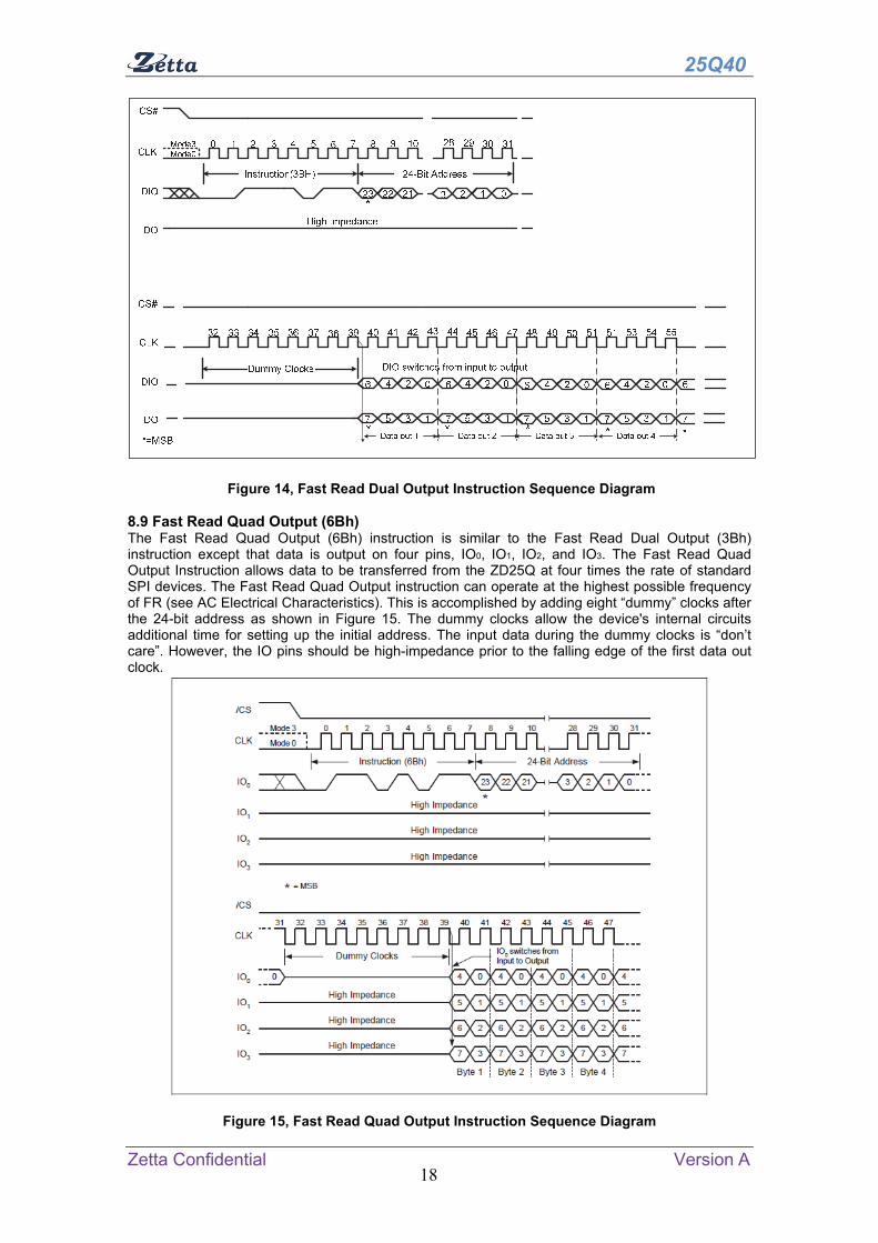
8.9 Fast Read Quad Output (6Bh) The Fast Read Quad Output (6Bh) instruction is similar to the Fast Read Dual Output (3Bh) instruction except that data is output on four pins, IO0, IO1, IO2, and IO3. The Fast Read Quad Output Instruction allows data to be transferred from the ZD25Q at four times the rate of standard SPI devices. The Fast Read Quad Output instruction can operate at the highest possible frequency of FR (see AC Electrical Characteristics). This is accomplished by adding eight “dummy” clocks after the 24-bit address as shown in Figure 15. The dummy clocks allow the device's internal circuits additional time for setting up the initial address. The input data during the dummy clocks is “don’t care”. However, the IO pins should be high-impedance prior to the falling edge of the first data out clock.
Figure 15, Fast Read Quad Output Instruction Sequence Diagram

25Q40
Zetta Confidential Version A 19
8.10 Fast Read Dual I/O (BBh) The Dual I/O Fast Read command is similar to the Dual Output Fast Read command but with the capability to input the 3-byte address (A23-0) and a “Continuous Read Mode” byte 2-bit per clock by SI and SO, each bit being latched in during the rising edge of SCLK, then the memory contents are shifted out 2-bit per clock cycle from SI and SO. The command sequence is shown in followed Figure 16. The first byte addressed can be at any location. The address is automatically incremented to the next higher address after each byte of data is shifted out. Dual I/O Fast Read with“Continuous Read Mode” The Dual I/O Fast Read command can further reduce command overhead through setting the “Continuous Read Mode” bits (M7-4) after the input 3-byte address (A23-A0). If the “Continuous Read Mode” bits (M5-4) = (1, 0), then the next Dual I/O Fast Read command (after CS# is raised and then lowered) does not require the BBH command code. The command sequence is shown in followed Figure 17. If the “Continuous Read Mode” bits (M5-4) do not equal (1, 0), the next command requires the first BBH command code, thus returning to normal operation. A “Continuous Read Mode” Reset command can be used to reset (M5-4) before issuing normal command.
Figure 16, Dual I/O Fast Read Sequence Diagram (M5-4 ≠ (1, 0))
Figure 17, Dual I/O Fast Read Sequence Diagram (M5-4 = (1, 0))
25Q40
Zetta Confidential Version A 20
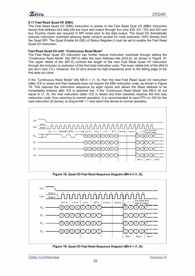
8.11 Fast Read Quad I/O (EBh) The Fast Read Quad I/O (EBh) instruction is similar to the Fast Read Dual I/O (BBh) instruction except that address and data bits are input and output through four pins IO0, IO1, IO2 and IO3 and four Dummy clocks are required in SPI mode prior to the data output. The Quad I/O dramatically reduces instruction overhead allowing faster random access for code execution (XIP) directly from the Quad SPI. The Quad Enable bit (QE) of Status Register-2 must be set to enable the Fast Read Quad I/O Instruction. Fast Read Quad I/O with “Continuous Read Mode” The Fast Read Quad I/O instruction can further reduce instruction overhead through setting the “Continuous Read Mode” bits (M7-0) after the input Address bits (A23-0), as shown in Figure 18. The upper nibble of the (M7-4) controls the length of the next Fast Read Quad I/O instruction through the inclusion or exclusion of the first byte instruction code. The lower nibble bits of the (M3-0) are don’t care (“x”). However, the IO pins should be high-impedance prior to the falling edge of the first data out clock. If the “Continuous Read Mode” bits M5-4 = (1, 0), then the next Fast Read Quad I/O instruction (after /CS is raised and then lowered) does not require the EBh instruction code, as shown in Figure 19. This reduces the instruction sequence by eight clocks and allows the Read address to be immediately entered after /CS is asserted low. If the “Continuous Read Mode” bits M5-4 do not equal to (1, 0), the next instruction (after /CS is raised and then lowered) requires the first byte instruction code, thus returning to normal operation. It is recommended to input FFh on IO0 for the next instruction (8 clocks), to ensure M4 = 1 and return the device to normal operation.
Figure 18, Quad I/O Fast Read Sequence Diagram (M5-4 ≠ (1, 0))
Figure 19, Quad I/O Fast Read Sequence Diagram (M5-4 = (1, 0))

25Q40
Zetta Confidential Version A 21
Quad I/O Fast Read with “8/16/32/64-Byte Wrap Around” in Standard SPI mode The Quad I/O Fast Read command can be used to access a specific portion within a page by issuing “Set Burst with Wrap” (77H) commands prior to EBH. The “Set Burst with Wrap” (77H) command can either enable or disable the “Wrap Around” feature for the following EBH commands. When “Wrap Around” is enabled, the data being accessed can be limited to either an8/16/32/64-byte section of a 256-byte page. The output data starts at the initial address specified in the command, once it reaches the ending boundary of the 8/16/32/64-byte section, the output will wrap around the beginning boundary automatically until CS# is pulled high to terminate the command. The Burst with Wrap feature allows applications that use cache to quickly fetch a critical address and then fill the cache afterwards within a fixed length (8/16/32/64-byte) of data without issuing multiple read commands. The “Set Burst with Wrap” command allows three “Wrap Bits” W6-W4 to be set. The W4 bit is used to enable or disable the “Wrap Around” operation while W6-W5 is used to specify the length of the wrap around section within a page. 8.12 Quad I/O Word Fast Read (E7H) The Quad I/O Word Fast Read command is similar to the Quad I/O Fast Read command except that the lowest address bit (A0) must equal 0 and only 2-dummy clock. The command sequence is shown in followed Figure 20. The first byte addressed can be at any location. The address is automatically incremented to the next higher address after each byte of data is shifted out. The Quad Enable bit (QE) of Status Register (S9) must be set to enable for the Quad I/O Word Fast read command. Quad I/O Word Fast Read with “Continuous Read Mode” The Quad I/O Word Fast Read command can further reduce command overhead through setting the “Continuous Read Mode” bits (M7-0) after the input 3-byte address (A23-A0). If the “Continuous Read Mode” bits (M5-4) = (1, 0), then the next Quad I/O Word Fast Read command (after CS# is raised and then lowered) does not require the E7H command code. The command sequence is shown in followed Figure 21. If the “Continuous Read Mode” bits (M5-4) do not equal to (1, 0), the next command requires the first E7H command code, thus returning to normal operation. A “Continuous Read Mode” Reset command can be used to reset (M5-4) before issuing normal command.
Figure 20, Quad I/O Word Fast Read Sequence Diagram (M5-4≠ (1, 0))

25Q40
Zetta Confidential Version A 22
Figure 21, Quad I/O Word Fast Read Sequence Diagram (M5-4= (1, 0))
Quad I/O Word Fast Read with “8/16/32/64-Byte Wrap Around” in Standard SPI mode The Quad I/O Word Fast Read command can be used to access a specific portion within a page by issuing “Set Burst with Wrap” (77H) commands prior to E7H. The “Set Burst with Wrap” (77H) command can either enable or disable the “Wrap Around” feature for the following E7H commands. When “Wrap Around” is enabled, the data being accessed can be limited to either an 8/16/32/64-byte section of a 256-byte page. The output data starts at the initial address specified in the command, once it reaches the ending boundary of the 8/16/32/64-byte section, the output will wrap around the beginning boundary automatically until CS# is pulled high to terminate the command. The Burst with Wrap feature allows applications that use cache to quickly fetch a critical address and then fill the cache afterwards within a fixed length (8/16/32/64-byte) of data without issuing multiple read commands. The “Set Burst with Wrap” command allows three “Wrap Bits” W6-W4 to be set. The W4 bit is used to enable or disable the “Wrap Around” operation while W6-W5 is used to specify the length of the wrap around section within a page. 8.13 Set Burst with Wrap (77H) The Set Burst with Wrap command is used in conjunction with “Quad I/O Fast Read” and “Quad I/O Word Fast Read” command to access a fixed length of 8/16/32/64-byte section within a 256-byte page, in standard SPI mode. The Set Burst with Wrap command sequence: CS# goes low Send Set Burst with Wrap command Send 24 dummy bits Send 8 bits “Wrap bits” CS# goes high.
If the W6-W4 bits are set by the Set Burst with Wrap command, all the following “Quad I/O Fast Read” and “Quad I/O Word Fast Read” command will use the W6-W4 setting to access the 8/16/32/64-byte section within any page. To exit the “Wrap Around” function and return to normal read operation, another Set Burst with Wrap command should be issued to set W4=1.
25Q40
Zetta Confidential Version A 23
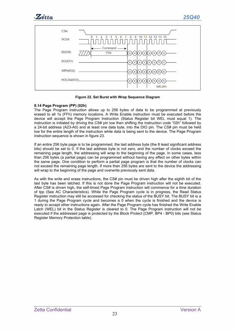
Figure 22. Set Burst with Wrap Sequence Diagram 8.14 Page Program (PP) (02h) The Page Program instruction allows up to 256 bytes of data to be programmed at previously erased to all 1s (FFh) memory locations. A Write Enable instruction must be executed before the device will accept the Page Program Instruction (Status Register bit WEL must equal 1). The instruction is initiated by driving the CS# pin low then shifting the instruction code “02h” followed by a 24-bit address (A23-A0) and at least one data byte, into the DIO pin. The CS# pin must be held low for the entire length of the instruction while data is being sent to the device. The Page Program instruction sequence is shown in figure 23. If an entire 256 byte page is to be programmed, the last address byte (the 8 least significant address bits) should be set to 0. If the last address byte is not zero, and the number of clocks exceed the remaining page length, the addressing will wrap to the beginning of the page. In some cases, less than 256 bytes (a partial page) can be programmed without having any effect on other bytes within the same page. One condition to perform a partial page program is that the number of clocks can not exceed the remaining page length. If more than 256 bytes are sent to the device the addressing will wrap to the beginning of the page and overwrite previously sent data. As with the write and erase instructions, the CS# pin must be driven high after the eighth bit of the last byte has been latched. If this is not done the Page Program instruction will not be executed. After CS# is driven high, the self-timed Page Program instruction will commence for a time duration of tpp (See AC Characteristics). While the Page Program cycle is in progress, the Read Status Register instruction may still be accessed for checking the status of the BUSY bit. The BUSY bit is a 1 during the Page Program cycle and becomes a 0 when the cycle is finished and the device is ready to accept other instructions again. After the Page Program cycle has finished the Write Enable Latch (WEL) bit in the Status Register is cleared to 0. The Page Program instruction will not be executed if the addressed page is protected by the Block Protect (CMP, BP4 - BP0) bits (see Status Register Memory Protection table).

25Q40
Zetta Confidential Version A 24
Figure 23, Page Program Instruction Sequence Diagram
8.15 Quad Input Page Program (32h) The Quad Page Program instruction allows up to 256 bytes of data to be programmed at previously erased (FFh) memory locations using four pins: IO0, IO1, IO2, and IO3. The Quad Page Program can improve performance for PROM Programmer and applications that have slow clock speeds <5MHz. Systems with faster clock speed will not realize much benefit for the Quad Page Program instruction since the inherent page program time is much greater than the time it take to clock-in the data. To use Quad Page Program the Quad Enable in Status Register-2 must be set (QE=1). A Write Enable instruction must be executed before the device will accept the Quad Page Program instruction (Status Register-1, WEL=1). The instruction is initiated by driving the /CS pin low then shifting the instruction code “32h” followed by a 24-bit address (A23-A0) and at least one data byte, into the IO pins. The /CS pin must be held low for the entire length of the instruction while data is being sent to the device. All other functions of Quad Page Program are identical to standard Page Program. The Quad Page Program instruction sequence is shown in Figure 24.
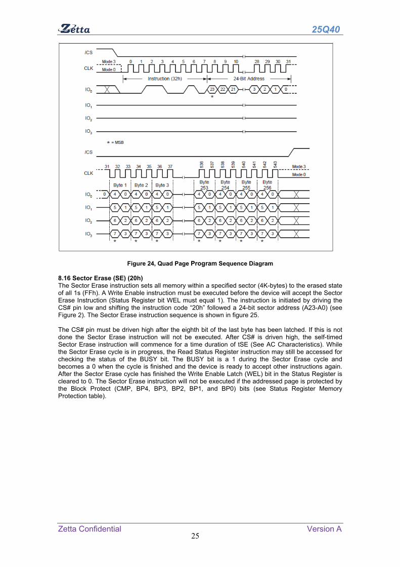
25Q40
Zetta Confidential Version A 25
Figure 24, Quad Page Program Sequence Diagram 8.16 Sector Erase (SE) (20h) The Sector Erase instruction sets all memory within a specified sector (4K-bytes) to the erased state of all 1s (FFh). A Write Enable instruction must be executed before the device will accept the Sector Erase Instruction (Status Register bit WEL must equal 1). The instruction is initiated by driving the CS# pin low and shifting the instruction code “20h” followed a 24-bit sector address (A23-A0) (see Figure 2). The Sector Erase instruction sequence is shown in figure 25. The CS# pin must be driven high after the eighth bit of the last byte has been latched. If this is not done the Sector Erase instruction will not be executed. After CS# is driven high, the self-timed Sector Erase instruction will commence for a time duration of tSE (See AC Characteristics). While the Sector Erase cycle is in progress, the Read Status Register instruction may still be accessed for checking the status of the BUSY bit. The BUSY bit is a 1 during the Sector Erase cycle and becomes a 0 when the cycle is finished and the device is ready to accept other instructions again. After the Sector Erase cycle has finished the Write Enable Latch (WEL) bit in the Status Register is cleared to 0. The Sector Erase instruction will not be executed if the addressed page is protected by the Block Protect (CMP, BP4, BP3, BP2, BP1, and BP0) bits (see Status Register Memory Protection table).

25Q40
Zetta Confidential Version A 26
Figure 25, Sector Erase Instruction Sequence Diagram 8.17 Block Erase (BE) (D8h) and Half Block Erase (52h) The Block Erase instruction sets all memory within a specified block (64K-bytes) or half block (32K-bytes) to the erased state of all 1s (FFh). A Write Enable instruction must be executed before the device will accept the Block Erase Instruction (Status Register bit WEL must equal 1). The instruction is initiated by driving the CS# pin low and shifting the instruction code “D8h” or “52h” followed a 24-bit block address (A23-A0) (see Figure 2). The Block Erase instruction sequence is shown in figure 26. The CS# pin must be driven high after the eighth bit of the last byte has been latched. If this is not done the Block Erase instruction will not be executed. After CS# is driven high, the self-timed Block Erase instruction will commence for a time duration of tBE (See AC Characteristics). While the Block Erase cycle is in progress, the Read Status Register instruction may still be accessed for checking the status of the BUSY bit. The BUSY bit is a 1 during the Block Erase cycle and becomes a 0 when the cycle is finished and the device is ready to accept other instructions again. After the Block Erase cycle has finished the Write Enable Latch (WEL) bit in the Status Register is cleared to 0. The Block Erase instruction will not be executed if the addressed page is protected by the Block Protect (CMP, BP4, BP3, BP2, BP1, and BP0) bits (see Status Register Memory Protection table).
Figure 26. Block Erase Instruction Sequence Diagram

25Q40
Zetta Confidential Version A 27
8.18 Chip Erase (CE) (C7h or 60h) The Chip Erase instruction sets all memory within the device to the erased state of all 1s (FFh). A Write Enable instruction must be executed before the device will accept the Chip Erase Instruction (Status Register bit WEL must equal 1). The instruction is initiated by driving the CS# pin low and shifting the instruction code “C7h” or “60h”. The Chip Erase instruction sequence is shown in figure 27. The CS# pin must be driven high after the eighth bit has been latched. If this is not done the Chip Erase instruction will not be executed. After CS# is driven high, the self-timed Chip Erase instruction will commence for a time duration of tCE (See AC Characteristics). While the Chip Erase cycle is in progress, the Read Status Register instruction may still be accessed to check the status of the BUSY bit. The BUSY bit is a 1 during the Chip Erase cycle and becomes a 0 when finished and the device is ready to accept other instructions again. After the Chip Erase cycle has finished the Write Enable Latch (WEL) bit in the Status Register is cleared to 0. The Chip Erase instruction will not be executed if any page is protected by the Block Protect (CMP, BP4, BP3, BP2, BP1, and BP0) bits (see Status Register Memory Protection table).
Figure 27, Chip Erase Instruction Sequence Diagram
8.19 Deep Power-down (DP) (B9h) Although the standby current during normal operation is relatively low, standby current can be further reduced with the Power-down instruction. The lower power consumption makes the Power-down instruction especially useful for battery powered applications (See ICC1 and ICC2 in AC Characteristics). The instruction is initiated by driving the CS# pin low and shifting the instruction code “B9h” as shown in figure 28. The CS# pin must be driven high after the eighth bit has been latched. If this is not done the Power-down instruction will not be executed. After CS# is driven high, the power-down state will enter within the time duration of tDP (See AC Characteristics). While in the power-down state only the Release from Power-down / Device ID instruction, which restores the device to normal operation, will be recognized. All other instructions are ignored. This includes the Read Status Register instruction, which is always available during normal operation. Ignoring all but one instruction makes the Power Down state a useful condition for securing maximum write protection. The device always powers-up in the normal operation with the standby current of ICC1.
Figure 28, Deep Power-down Instruction Sequence Diagram
8.20 Release Power-down / Device ID (ABh) The Release from Power-down / Device ID instruction is a multi-purpose instruction. It can be used to release the device from the power-down state, obtain the devices electronic identification (ID) number or do both.
25Q40
Zetta Confidential Version A 28
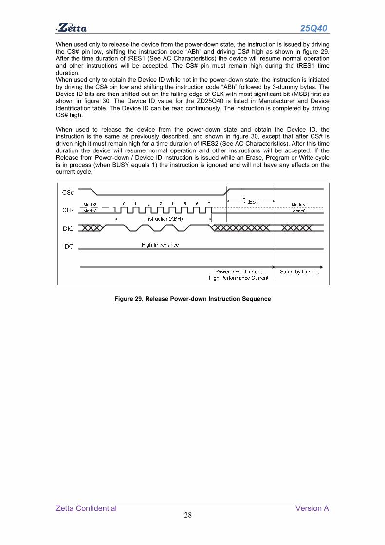
When used only to release the device from the power-down state, the instruction is issued by driving the CS# pin low, shifting the instruction code “ABh” and driving CS# high as shown in figure 29. After the time duration of tRES1 (See AC Characteristics) the device will resume normal operation and other instructions will be accepted. The CS# pin must remain high during the tRES1 time duration. When used only to obtain the Device ID while not in the power-down state, the instruction is initiated by driving the CS# pin low and shifting the instruction code “ABh” followed by 3-dummy bytes. The Device ID bits are then shifted out on the falling edge of CLK with most significant bit (MSB) first as shown in figure 30. The Device ID value for the ZD25Q40 is listed in Manufacturer and Device Identification table. The Device ID can be read continuously. The instruction is completed by driving CS# high. When used to release the device from the power-down state and obtain the Device ID, the instruction is the same as previously described, and shown in figure 30, except that after CS# is driven high it must remain high for a time duration of tRES2 (See AC Characteristics). After this time duration the device will resume normal operation and other instructions will be accepted. If the Release from Power-down / Device ID instruction is issued while an Erase, Program or Write cycle is in process (when BUSY equals 1) the instruction is ignored and will not have any effects on the current cycle.
Figure 29, Release Power-down Instruction Sequence

25Q40
Zetta Confidential Version A 29
Figure 30, Release Power-down / Device ID Instruction Sequence Diagram
8.21 Read Manufacturer / Device ID (90h) The Read Manufacturer/Device ID instruction is an alternative to the Release from Power-down /Device ID instruction that provides both the JEDEC assigned manufacturer ID and the specific device ID. The Read Manufacturer/Device ID instruction is very similar to the Release from Power-down / Device ID instruction. The instruction is initiated by driving the CS# pin low and shifting the instruction code “90h” followed by a 24-bit address (A23-A0) of 000000h. After which, the Manufacturer ID for Zetta(XXh) and the Device ID are shifted out on the falling edge of CLK with most significant bit (MSB) first as shown in Figure 31. The Device ID values for the ZD25Q40 are listed in Table 5. If the 24-bit address is initially set to 000001h the Device ID will be read first.
Figure 31, Read Manufacturer / Device ID Diagram

25Q40
Zetta Confidential Version A 30
8.22 Read Identification (RDID) (9Fh) For compatibility reasons, the ZD25Q40 provides several instructions to electronically determine the identity of the device. The Read JEDEC ID instruction is compatible with the JEDEC standard for SPI compatible serial memories that was adopted in 2003. The instruction is initiated by driving the CS# pin low and shifting the instruction code “9Fh”. The JEDEC assigned Manufacturer ID byte for Zetta Device (XXh) and two Device ID bytes, Memory Type (ID15-ID8) and Capacity (ID7-ID0) are then shifted out on the falling edge of CLK with most significant bit (MSB) first as shown in figure 32. For memory type and capacity values refer to Manufacturer and Device Identification table.
CS#
CLK Mode0Mode3 0 1 15141312111098765432
DIO
Instruction(9FH)
DO
Manufacturer ID
*
High Impedance
CS#
CLK16 17 3130292827262524232221201918 Mode3
Mode0
DIO
Memory Type ID15-ID8
DO
**=MSB
7 6 5 4 3 2 1 0
7 6 5 4 3 2 1 07 6 5 4 3 2 1 0
Capacity ID7-ID0
*
Figure 32, Read JEDEC ID instruction Sequence Diagram
8.23 Enable Reset (66h) and Reset (99h) The ZD25Q40 provide a software Reset instruction instead of a dedicated RESET pin. Once the Reset instruction is accepted, any on-going internal operations will be terminated and the device will return to its default power-on state and lose all the current volatile settings, such as Volatile Status Register bits, Write Enable Latch (WEL) status, Program/Erase Suspend status, Read parameter setting (P7-P0), Continuous Read Mode bit setting (M7-M0) and Wrap Bit setting (W6-W4). “Enable Reset (66h)” and “Reset (99h)” instructions can be issued in SPI mode. To avoid accidental reset, both instructions must be issued in sequence. Any other commands other than “Reset (99h)” after the “Enable Reset (66h)” command will disable the “Reset Enable” state. A new sequence of “Enable Reset (66h)” and “Reset (99h)” is needed to reset the device. Once the Reset command is accepted by the device, the device will take approximately tRST=30us to reset. During this period, no command will be accepted. Data corruption may happen if there is an on-going or suspended internal Erase or Program operation when Reset command sequence is accepted by the device. It is recommended to check the BUSY bit in Status Register before issuing the Reset command sequence.

25Q40
Zetta Confidential Version A 31
Figure 33. Enable Reset and Reset command Sequence Diagram

25Q40
Zetta Confidential Version A 32
9 ELECTRICAL CHARACTERISTICS
9.1 Power-up Timing
Figure 34, Power-up Timing
Table 6, Power-up Timing
MIN MAXVcc(min) to CS# Low tVSL(1) 10 μs
Time Delay Before Write Instruction tPUW(1) 1 10 ms
Write Inhibit Threshold Voltage VWI(1) 1 2 V
TYPESYMBOLPARAMETER UNIT
Note: 1.The parameters are characterized only. 2. VCC (max.) is 3.6V and VCC (min.) is 2.7V
9.2 Absolute Maximum Ratings Stresses above the values so mentioned above may cause permanent damage to the device. These values are for a stress rating only and do not imply that the device should be operated at conditions up to or above these values.
Table 7, Absolute Maximum Ratings
PARAMETERS SYMBOL CONDITIONS RANGE UNIT
Supply Voltage VCC -0.6 to +4.0 V
Voltage applied on any pin VIO Relative to Ground -0.6 to VCC+0.4 V
Transient Voltage on any Pin VIOT<20ns Transient Relative
to Ground-2.0 to VCC+2.0 V
Storage Temperature TSTG -65 to +150 ℃Lead Temprature TLEAD See Note(3) ℃Electrostatic Discharge Voltage VESD Human Body Model(4) -2000 to +2000 V
25Q40
Zetta Confidential Version A 33
Notes: 1. Specification for ZD25Q40 is preliminary. See preliminary designation at the end of this document. 2. This device has been designed and tested for the specified operation ranges. Proper operation outside of these levels is not guaranteed. Exposure to absolute maximum ratings may affect device reliability. Exposure beyond absolute maximum ratings may cause permanent damage. 3. Compliant with JEDEC Standard J-STD-20C for small body Sn-Pb or Pb-free (Green) assembly and the European directive on restrictions on hazardous substances (RoHS) 2002/95/EU. 4. JEDEC Std JESD22-A114A (C1=100 pF, R1=1500 ohms, R2=500 ohms).
9.3 INITIAL DELIVERY STATE The device is delivered with the memory array erased: all bits are set to 1(each byte contains FFH). The Status Register bits are set to 0.
9.4 Recommended Operating Ranges
Table 8, Recommended Operating Ranges
PARAMETER SYMBOL CONDITIONS SPEC
UNIT MIN MAX
Supply Voltage VCC FR=108MHz,fR=50MHz 2.7 3.6 V
Ambient Temperature, Operating
TA Industrial -40 +85 ℃
Notes: 1. Recommended Operating Ranges define those limits between which the functionality of the device is guaranteed.

25Q40
Zetta Confidential Version A 34
9.5 DC Characteristics
Table 9. DC Characteristics
Notes: 1. Tested on sample basis and specified through design and characterization data. TA=25° C, VCC 3V. 2. Checker Board Pattern.
9.6 AC Measurement Conditions
Table 10, AC Measurement Conditions
Symbol PARAMETER Min. Max. Unit CL Load Capacitance 30 pF TR, TF Input Rise and Fall Times 5 ns VIN Input Pulse Voltages 0.2VCC to 0.8VCC V VtIN Input Timing Reference Voltages 0.3VCC to 0.7VCC V VtON Output Timing Reference Voltages 0.5 VCC to 0.5 VCC V
Figure 35, AC Measurement I/O Waveform
SYMBOL PARAMETER CONDITIONSSPEC
UNIT MIN TYP MAX
ILI Input Leakage ±2 μA ILO I/O Leakage ±2 μA
ICC1 Standby Current CS# = VCC, VIN = GND or VCC
1 5 μA
ICC2 Power-down Current CS# = VCC, VIN = GND or VCC
1 5 μA
ICC3 Operating Current (Read)
CLK=0.1VCC / 0.9VCC at 108MHz, Q=Open(*1,*2,*4 I/O)
15 20 mA
CLK=0.1VCC / 0.9VCC at 80MHz, Q=Open(*1,*2,*4 I/O)
13 18 mA
ICC4 Current Page Program
CS# = VCC 20 mA
ICC5 Current Write Status Register
CS# = VCC 20 mA
ICC6 Current Sector/Block Erase
CS# = VCC 20 mA
ICC7 Current Chip Erase CS# = VCC 20 mA VIL Input Low Voltage –0.5 VCC x 0.2 V VIH Input High Voltage VCC x0.7 VCC +0.4 V VOL Output Low Voltage IOL = 100uA 0.2 V VOH Output High Voltage IOH = –100 μA VCC –0.2 VCC V
25Q40
Zetta Confidential Version A 35
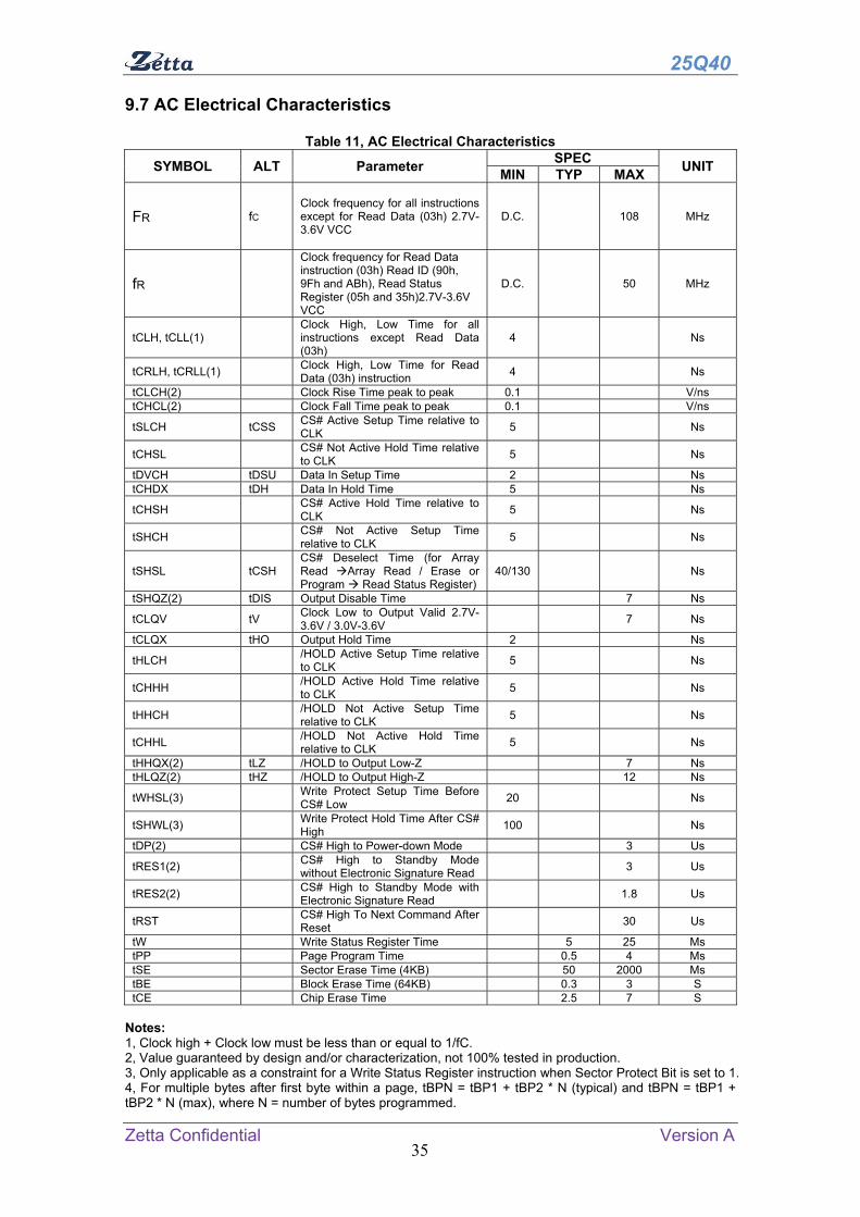
9.7 AC Electrical Characteristics
Table 11, AC Electrical Characteristics
SYMBOL ALT Parameter SPEC
UNIT MIN TYP MAX
FR fC Clock frequency for all instructions except for Read Data (03h) 2.7V-3.6V VCC
D.C. 108 MHz
fR
Clock frequency for Read Data instruction (03h) Read ID (90h, 9Fh and ABh), Read Status Register (05h and 35h)2.7V-3.6V VCC
D.C. 50 MHz
tCLH, tCLL(1) Clock High, Low Time for all instructions except Read Data (03h)
4 Ns
tCRLH, tCRLL(1) Clock High, Low Time for Read Data (03h) instruction
4 Ns
tCLCH(2) Clock Rise Time peak to peak 0.1 V/ns tCHCL(2) Clock Fall Time peak to peak 0.1 V/ns
tSLCH tCSS CS# Active Setup Time relative to CLK
5 Ns
tCHSL CS# Not Active Hold Time relative to CLK
5 Ns
tDVCH tDSU Data In Setup Time 2 Ns tCHDX tDH Data In Hold Time 5 Ns
tCHSH CS# Active Hold Time relative to CLK
5 Ns
tSHCH CS# Not Active Setup Time relative to CLK
5 Ns
tSHSL tCSH CS# Deselect Time (for Array Read Array Read / Erase or Program Read Status Register)
40/130 Ns
tSHQZ(2) tDIS Output Disable Time 7 Ns
tCLQV tV Clock Low to Output Valid 2.7V-3.6V / 3.0V-3.6V
7 Ns
tCLQX tHO Output Hold Time 2 Ns
tHLCH /HOLD Active Setup Time relative to CLK
5 Ns
tCHHH /HOLD Active Hold Time relative to CLK
5 Ns
tHHCH /HOLD Not Active Setup Time relative to CLK
5 Ns
tCHHL /HOLD Not Active Hold Time relative to CLK
5 Ns
tHHQX(2) tLZ /HOLD to Output Low-Z 7 Ns tHLQZ(2) tHZ /HOLD to Output High-Z 12 Ns
tWHSL(3) Write Protect Setup Time Before CS# Low
20 Ns
tSHWL(3) Write Protect Hold Time After CS# High
100 Ns
tDP(2) CS# High to Power-down Mode 3 Us
tRES1(2) CS# High to Standby Mode without Electronic Signature Read
3 Us
tRES2(2) CS# High to Standby Mode with Electronic Signature Read
1.8 Us
tRST CS# High To Next Command After Reset
30 Us
tW Write Status Register Time 5 25 Ms tPP Page Program Time 0.5 4 Ms tSE Sector Erase Time (4KB) 50 2000 Ms tBE Block Erase Time (64KB) 0.3 3 S tCE Chip Erase Time 2.5 7 S
Notes: 1, Clock high + Clock low must be less than or equal to 1/fC. 2, Value guaranteed by design and/or characterization, not 100% tested in production. 3, Only applicable as a constraint for a Write Status Register instruction when Sector Protect Bit is set to 1. 4, For multiple bytes after first byte within a page, tBPN = tBP1 + tBP2 * N (typical) and tBPN = tBP1 + tBP2 * N (max), where N = number of bytes programmed.

25Q40
Zetta Confidential Version A 36
Figure 36, Serial Output Timing
Figure 37, Input Timing
Figure 38, Hold Timing

25Q40
Zetta Confidential Version A 37
10 PACKAGE MECHANICAL 8-Pin SOIC 150-mil
25Q40
Zetta Confidential Version A 38
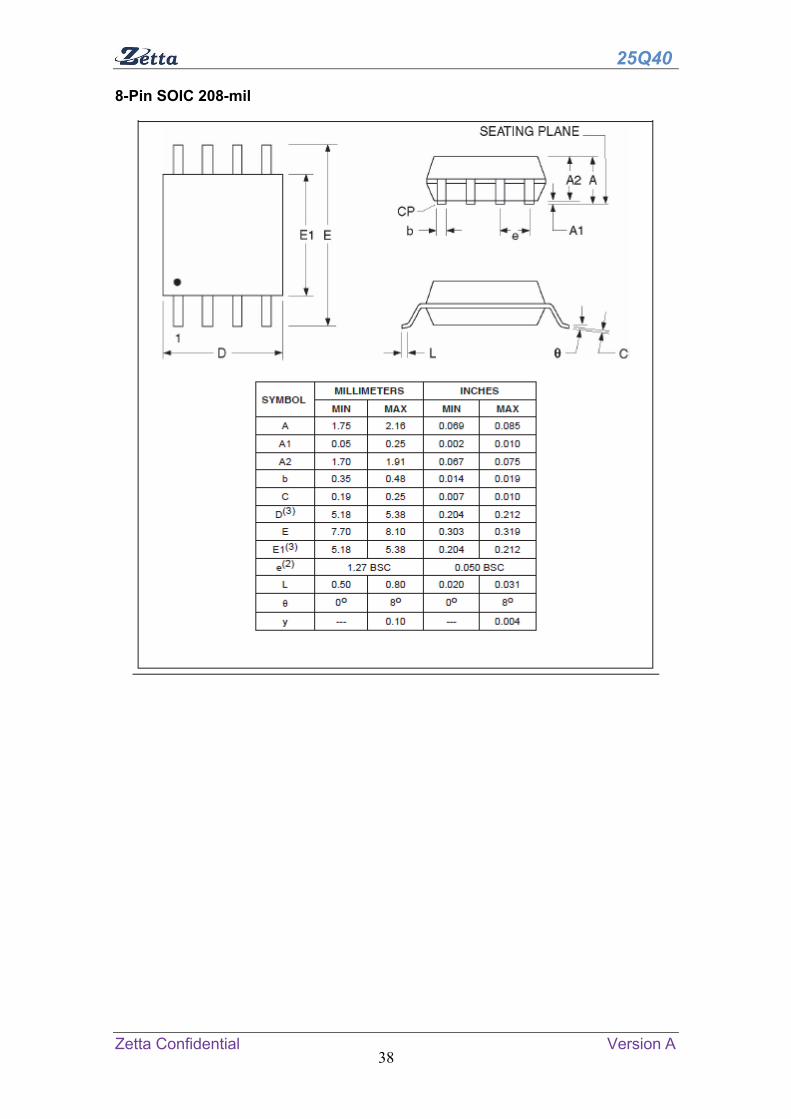
8-Pin SOIC 208-mil

25Q40
Zetta Confidential Version A 39
USON8 (3*2mm)
25Q40
Zetta Confidential Version A 40
USON8 (3*3mm, 0.65mm)
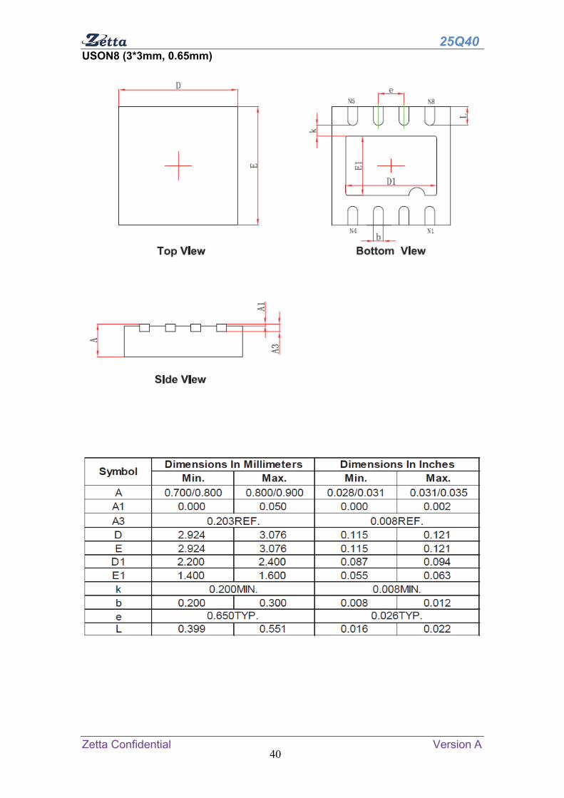
25Q40
Zetta Confidential Version A 41
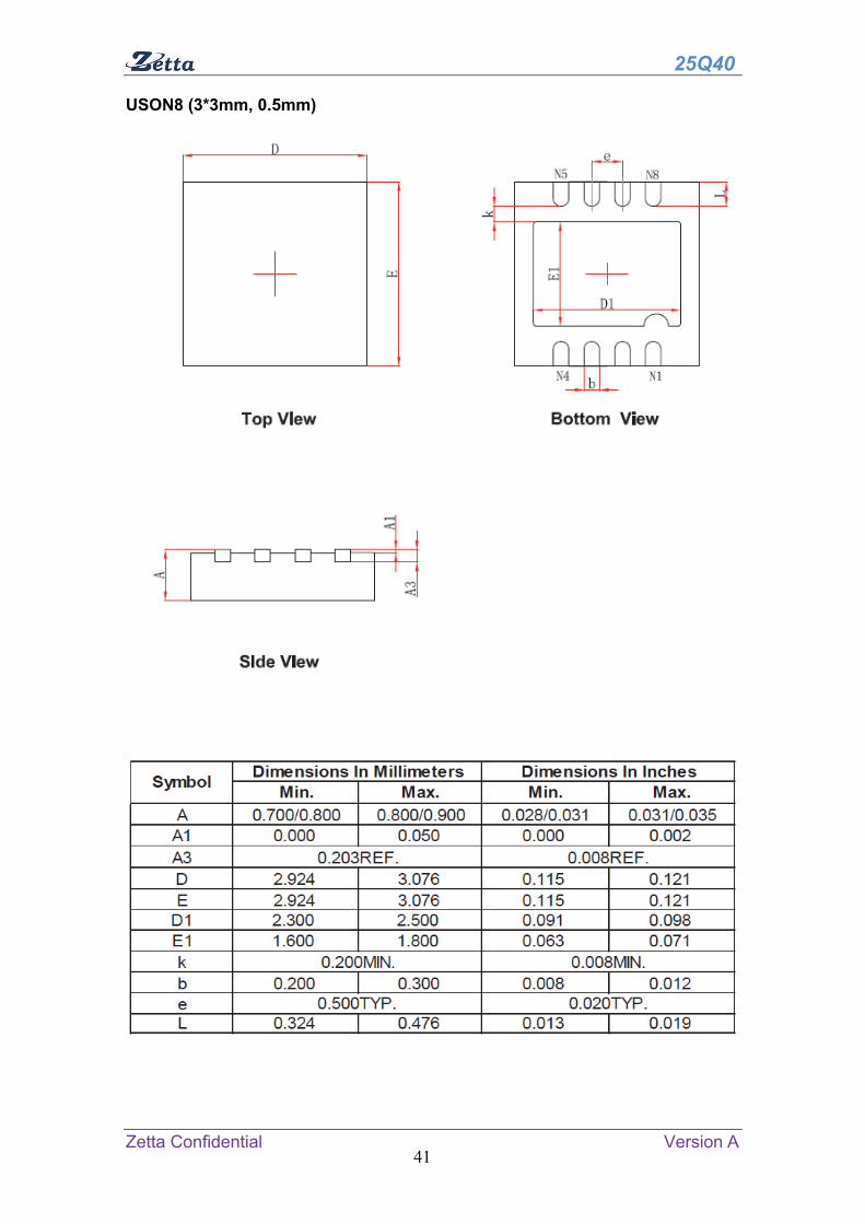
USON8 (3*3mm, 0.5mm)
25Q40
Zetta Confidential Version A 42
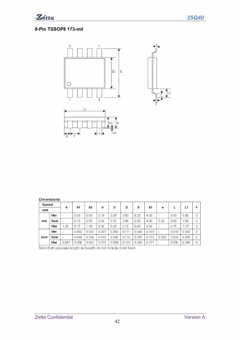
8-Pin TSSOP8 173-mil

25Q40
Zetta Confidential Version A 43
REVISION LIST
Version No. Description Date A0 Initial Release 2016-9-13