2.isca-rjengs-2013-092
DESCRIPTION
A New Active Power Factor Correction Controller using Boost ConverterTRANSCRIPT

Research Journal of Engineering
Vol. 2(8), 7-11, August (2013)
International Science Congress Association
A New Active Power Factor Correction Controller using Boost Converter
Department of Electrical and Electronics Engineering, Gokaraju Rangaraju
Bachupally , Kukatpally, Hyderabad, A.P, INDIA
Received 18th
July
Abstract
In an electrical Power systems, a load with a low power factor draws more current than a load with a high power factor for th
same amount of useful power transferred. Linear loads with low power factor (induction motor) can be corrected with a passive
network of capacitors or inductors. The hysteresis current controller is used to track the line current command.
loads (rectifier) distort the current drawn from the system. In this paper, Boost converter topology is used to accomplish th
active power factor correction in many discontinuous or continuous modes. Furthermore the start up current has been reduced.
Keywords: Power factor, boost converter, linear loads, power factor correction, border line control
Introduction
An ac to dc converter consists of a line frequency diode bridge
rectifier with a large output filter capacitor which is cheap and
robust and it demands a harmonic rich ac line current. So the
input power factor is poor1. The most common power quality
disturbance is instantaneous power interruption. Various power
factor correction (PFC) techniques are employed to overcome
these power quality problems out of which the boost converter
topology has been extensively used in various ac/dc and dc/dc
applications2. In fact, the front end of today’s ac/dc power
supplies with power-factor correction (PFC) is almost exclusively
implemented with boost topology3. The use of Power Factor
Correction (PFC) is necessary in order to comply the recent
international standards, such as IEC- 1000-3
The basic boost topology does not provide a high boost factor
This has led to many proposed topologies such as the tapped
inductor boost, cascaded boost and interleaved boost
This paper introduces another variation, Boost PFC Converter
which provides a higher boost factor and also provides proper
controlling both with hardware and software design. Here
Hysteresis Current Control method is used for better control
This paper initially involves simulation of basic conventional
rectifier circuits and the analysis of the current and voltage
waveforms. It starts with simple circuits and switches to advanced
circuits by implementing advanced techniques such as active PF
IC L6561 both with hardware and software and their subsequent
effect on the current and voltage waveforms expecting better
results. All the simulation work is carried out in MATlab
Simulink.
Mathematical Formulation
Boost Converter: The key principle that drives the boost
converter is the tendency of an inductor to resist changes in
current. In a boost converter, the output voltage is always higher
Engineering Sciences ___________________________________________
International Science Congress Association
A New Active Power Factor Correction Controller using Boost Converter
Sridevi J. Department of Electrical and Electronics Engineering, Gokaraju Rangaraju Institute of Engineering and Technology,
Bachupally , Kukatpally, Hyderabad, A.P, INDIA
Available online at: www.isca.in July 2013, revised 25
th July 2013, accepted 24
th August 2013
In an electrical Power systems, a load with a low power factor draws more current than a load with a high power factor for th
same amount of useful power transferred. Linear loads with low power factor (induction motor) can be corrected with a passive
The hysteresis current controller is used to track the line current command.
loads (rectifier) distort the current drawn from the system. In this paper, Boost converter topology is used to accomplish th
power factor correction in many discontinuous or continuous modes. Furthermore the start up current has been reduced.
Power factor, boost converter, linear loads, power factor correction, border line control.
An ac to dc converter consists of a line frequency diode bridge
rectifier with a large output filter capacitor which is cheap and
robust and it demands a harmonic rich ac line current. So the
. The most common power quality
disturbance is instantaneous power interruption. Various power
factor correction (PFC) techniques are employed to overcome
these power quality problems out of which the boost converter
d in various ac/dc and dc/dc
. In fact, the front end of today’s ac/dc power
factor correction (PFC) is almost exclusively
. The use of Power Factor
comply the recent
3-2 and IEEE-519.
The basic boost topology does not provide a high boost factor4.
This has led to many proposed topologies such as the tapped
inductor boost, cascaded boost and interleaved boost converters.
This paper introduces another variation, Boost PFC Converter
which provides a higher boost factor and also provides proper
controlling both with hardware and software design. Here
Hysteresis Current Control method is used for better control5.
This paper initially involves simulation of basic conventional
rectifier circuits and the analysis of the current and voltage
waveforms. It starts with simple circuits and switches to advanced
circuits by implementing advanced techniques such as active PFC
and their subsequent
effect on the current and voltage waveforms expecting better
results. All the simulation work is carried out in MATlab –
that drives the boost
to resist changes in
current. In a boost converter, the output voltage is always higher
than the input voltage6. When the switch is turned
current flows through the inductor and energy is stored in it.
When the switch is turned-OFF, the stored energy in the
inductor tends to collapse and its polarity changes such that it
adds to the input voltage as shown in Figure
voltage across the inductor and the input voltage are in series
and together charge the output capacitor to a voltage higher than
the input voltage7.
Figure
Boost Converter
The basic principle of a Boost converter as shown in Figure
consists of 2 distinct states: i. In the On
closed, resulting in an increase in the inductor current, ii. In the
Off-state, the switch is open and the only path offered to
inductor current is through the fly back diode
and the load R. This result in transferring the energy
accumulated during the On-state into the capacitor.
Continuous Mode: When a boost converter operates in
continuous mode, the current through the inductor (
falls to zero. Figure-3 shows the typical waveforms of currents
and voltages in a converter operating in continuous mode
output voltage can be calculated as follo
ideal converter operating in steady conditions.
________ ISSN 2278 – 9472
Res. J. Engineering Sci.
7
A New Active Power Factor Correction Controller using Boost Converter
Institute of Engineering and Technology,
In an electrical Power systems, a load with a low power factor draws more current than a load with a high power factor for the
same amount of useful power transferred. Linear loads with low power factor (induction motor) can be corrected with a passive
The hysteresis current controller is used to track the line current command. Non-linear
loads (rectifier) distort the current drawn from the system. In this paper, Boost converter topology is used to accomplish this
power factor correction in many discontinuous or continuous modes. Furthermore the start up current has been reduced.
. When the switch is turned-ON, the
current flows through the inductor and energy is stored in it.
OFF, the stored energy in the
inductor tends to collapse and its polarity changes such that it
adds to the input voltage as shown in Figure-1. Thus, the
across the inductor and the input voltage are in series
and together charge the output capacitor to a voltage higher than
Figure-1
Boost Converter
The basic principle of a Boost converter as shown in Figure-2
consists of 2 distinct states: i. In the On-state, the switch S is
closed, resulting in an increase in the inductor current, ii. In the
state, the switch is open and the only path offered to
fly back diode D, the capacitor C
and the load R. This result in transferring the energy
state into the capacitor.
boost converter operates in
continuous mode, the current through the inductor ( ) never
3 shows the typical waveforms of currents
and voltages in a converter operating in continuous mode8. The
output voltage can be calculated as follows, in the case of an
ideal converter operating in steady conditions.

Research Journal of Engineering Sciences___________
Vol. 2(8), 7-11, August (2013)
International Science Congress Association
Figure-2
Boost converter operation circuit
Figure-3
Continuous mode
Figure-4
Discontinuous mode
_________________________________________________
International Science Congress Association
Boost converter operation circuit
Dis Continuous Mode: If the ripple amplitude of the current is
too high, the inductor may be completely discharged before the
end of a whole commutation cycle
through the inductor falls to zero during part of the period as
shown in Figure-4. Although slight, the difference has a strong
effect on the output voltage equation. I
follows:
Figure-
Border line control
Power Factor Correction: The attention devoted to the quality
of the currents absorbed from the utility line by
equipment is increasing due to several reasons. In fact, a low
power factor reduces the power available from the utility grid,
while a high harmonic distortion of the line current causes EMI
problems and cross-interferences, through the line imp
between different systems connected to the same grid
An ideal power factor corrector (PFC) should emulate a resistor
on the supply side while maintaining a fairly regulated output
voltage. In the case of sinusoidal line voltage, this means that
the converter must draw a sinusoidal current from the utility; in
order to do that, a suitable sinusoidal reference is generally
needed and the control objective is to force the input current to
follow, as close as possible, this current reference
paper, a hardware design using IC having border line control is
used. Figure-5 shows the circuit diagram for border line control.
In this control approach the switch on
during the line cycle and the switch is turned on when the
_____________ ISSN 2278 – 9472
Res. J. Engineering Sci.
8
ripple amplitude of the current is
too high, the inductor may be completely discharged before the
end of a whole commutation cycle9. In this case, the current
through the inductor falls to zero during part of the period as
ht, the difference has a strong
effect on the output voltage equation. It can be calculated as
-5
Border line control
The attention devoted to the quality
of the currents absorbed from the utility line by electronic
equipment is increasing due to several reasons. In fact, a low
power factor reduces the power available from the utility grid,
while a high harmonic distortion of the line current causes EMI
interferences, through the line impedance,
between different systems connected to the same grid10
.
An ideal power factor corrector (PFC) should emulate a resistor
on the supply side while maintaining a fairly regulated output
voltage. In the case of sinusoidal line voltage, this means that
the converter must draw a sinusoidal current from the utility; in
order to do that, a suitable sinusoidal reference is generally
needed and the control objective is to force the input current to
follow, as close as possible, this current reference11
. In this
paper, a hardware design using IC having border line control is
5 shows the circuit diagram for border line control.
In this control approach the switch on-time is held constant
during the line cycle and the switch is turned on when the
Research Journal of Engineering Sciences___________
Vol. 2(8), 7-11, August (2013)
International Science Congress Association
inductor current falls to zero, so that the converter operates at
the boundary between Continuous and Discontinuous Inductor
Current Mode (CICM-DICM)12
. In this way, the freewheeling
diode is turned off softly (no recovery losses) and the switch is
turned on at zero current, so the commutation losses are
reduced. On the other hand the higher current peaks increase
device stresses and conduction losses and may call for heavier
input filters (for some topologies).
This type of control is a particular case of hysteretic control in
which the lower reference is zero anywhere.
Results and Discussions
This paper involves simulation of simple circuits with a gradual
increase in complexity by inclusion of new components
also the hardware implementation and their subsequent effect on
the current and voltage waveforms. The waveforms with
software and hardware are compared. All the simulation work is
done in MATLAB Simulink.
Figure-6
IC Implementation in MATLAB before PFC
Simulation and results for Conventional Converter:
shows that this circuit consists of two groups of diodes: top
group with diodes 1 and 3 and bottom groups with diodes 2 and
4. It is easy to see the operation of each group of diodes with Ls
=0. The current id flows continuously through one diode of the
top group and one diode in the bottom group.
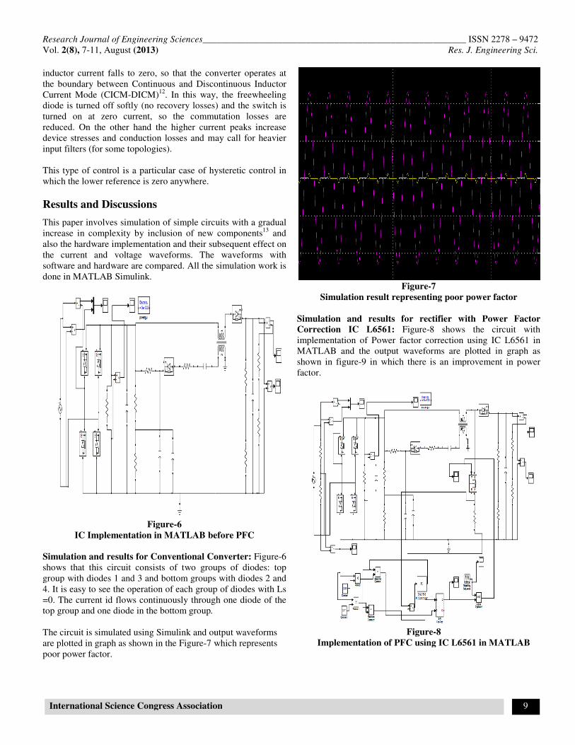
The circuit is simulated using Simulink and output waveforms
are plotted in graph as shown in the Figure-7 which represents
poor power factor.
_________________________________________________
International Science Congress Association
inductor current falls to zero, so that the converter operates at
the boundary between Continuous and Discontinuous Inductor
. In this way, the freewheeling
diode is turned off softly (no recovery losses) and the switch is
on at zero current, so the commutation losses are
reduced. On the other hand the higher current peaks increase
device stresses and conduction losses and may call for heavier
hysteretic control in
This paper involves simulation of simple circuits with a gradual
increase in complexity by inclusion of new components13
and
eir subsequent effect on
the current and voltage waveforms. The waveforms with
software and hardware are compared. All the simulation work is
IC Implementation in MATLAB before PFC
al Converter: Figure-6
shows that this circuit consists of two groups of diodes: top
group with diodes 1 and 3 and bottom groups with diodes 2 and
4. It is easy to see the operation of each group of diodes with Ls
through one diode of the
The circuit is simulated using Simulink and output waveforms
7 which represents
Figure-
Simulation result representing
Simulation and results for rectifier with Power Factor
Correction IC L6561: Figure-8 shows the circuit with
implementation of Power factor correction using IC L6561 in
MATLAB and the output waveforms are plotted in graph as
shown in figure-9 in which there is an improvement in power
factor.
Figure
Implementation of PFC using IC L6561 in MATLAB
_____________ ISSN 2278 – 9472
Res. J. Engineering Sci.
9
-7
Simulation result representing poor power factor
Simulation and results for rectifier with Power Factor
8 shows the circuit with
implementation of Power factor correction using IC L6561 in
MATLAB and the output waveforms are plotted in graph as
9 in which there is an improvement in power
Figure-8
Implementation of PFC using IC L6561 in MATLAB

Research Journal of Engineering Sciences________________________________________________________ ISSN 2278 – 9472
Vol. 2(8), 7-11, August (2013) Res. J. Engineering Sci.
International Science Congress Association 10
Figure-9
Simulation result representing improved power factor
Hardware results: Figure-10 shows the hardware circuit
without IC which results in poor power factor when
incandescent lamps are used as load observed in CRO.
Figure-10
Poor Supply p.f waveform using incandescent lamps as load
Figure-11
Voltage Boost across the load
Figure-12
Improved power factor
Figure-11 shows the boost voltage at load when boost converter
has used. Figure-12 shows the hardware circuit with IC which
results in improved power factor observed in CRO.
Conclusion
The Power Factor Correction with boost converter are simulated
with MATLAB Simulink and also hardware design is
implemented.. In this paper conventional converter, Boost
converter using border line Control is discussed. It is noticed
that the power Factor is better for Boost Converter Circuit. It is
observed that there is an improvement in power factor with
boost converter both in simulation as well as in hardware
implementation.
References
1. Hussain S., Athab P.K. and Shadhu Khan, A Cost
Effective Method of Reducing Total Harmonic Distortion
(THD) in Single-Phase Boost Rectifier, 1-4244-0645-
5/07IEEE (2007)
2. Tiago Kommers Jappe and Samir Ahmad Mussa, Current
control techniques applied in PFC boost converter at
instantaneous power interruption,- 978-1-4244-4649-0/09
IEEE (2009)
3. Shikha Singh G. and Bhuvaneswari Bhim Singh, Multiple
Output SMPS with Improved Input Power Quality - 978-1-
4244-6653-5/10 IEEE (2010)
4. Yungtaek Jang and Milan M. Jovanovic, High-Power-
Factor Soft-Switched Boost Converter IEEE Transactions
On Power Electronics, 21(1), (2006)
5. Attaianese, Nardi V., Parillo F. and Tomasso G.,
Predictive Control Of Parallel Boost Converters 978-1-
4244-1766-7/08 IEEE (2008)

Research Journal of Engineering Sciences________________________________________________________ ISSN 2278 – 9472
Vol. 2(8), 7-11, August (2013) Res. J. Engineering Sci.
International Science Congress Association 11
6. Van Rensburg J.F.J., Case M.J. and Nicolae D.V., Double-
Boost DC to DC Converter 978-1- 4244-1766-7/08 IEEE
(2008)
7. Yasunobu Suzuki, Toru Teshima Isao Sugawara Akira
Takeuchi, Experimental Studies on Active and Passive
PFC Circuits, 0-78'03-3996-7/97 IEEE (1997)
8. Paul Nosike Ekemezie, Design Of A Power Factor
Correction AC-DC Converter, 1-4244-0987-X/07 IEEE
(2007)
9. Vishwanathan N. and Ramanarayanan V., Average Current
Mode Control of High Voltage DC Power Supply for
Pulsed Load Application, 0-7803-7420-7/02 IEEE (2002)
10. Fadnavis Shubham, A Design of GUI Based Wireless
Robotic Car, Research Journal of Engineering Sciences,
1(2), 26-31, (2012)
11. Perumal R.1 and Saravanan K., Comparison of
Hydrodynamic Behavior of Jet Mixer for Newtonian and
Non-Newtonian Fluids”, Research Journal of Engineering
Sciences, 1(3), 45-51 (2012)
12. Sharma Pankaj and Kumar Nittin, Temperature Response
of Cellular Network Based Concentric Tube Heat
Exchanger for Concurrent Flow Using Matlab/Simulink,
Research Journal of Engineering Sciences, 2(5), 19-23
(2013)
13. Jain Sandesh, Thakur Shivendra Singh and Phulambrikar
S.P., Improve Power Factor and Reduce the Harmonics
Distortion of the System”, Research Journal of
Engineering Sciences, 1(5), 31-36 (2012)
14. Gupta Rajani, Mehta Alok K. and Tiwari Vebhav, Vocoder
(LPC) Analysis by Variation of Input Parameters and
Signals, ISCA Journal of Engineering Sciences, 1(1), 57-
61 (2012)