30-w/in^3, 94% efficiency, 65-w usb type-c pd ac/dc
TRANSCRIPT

CSD17575
EMI &
Bridge
Rectifier
85~264
VAC
ISO7710F
UCC28780OPT
OATL431
UCC24612TPS25740B
TPD1E05U06
Vout
RTN
CC1/CC2
GAN
GAN
Q2
1TIDUDW2C–February 2018–Revised June 2020Submit Documentation Feedback
Copyright © 2018–2020, Texas Instruments Incorporated
30-W/in3, 94% Efficiency, 65-W USB Type-C™ PD AC/DC AdapterReference Design
Design Guide: TIDA-0162230-W/in3, 94% Efficiency, 65-W USB Type-C™ PD AC/DCAdapter Reference Design
DescriptionThis fully-tested, USB power delivery reference designis a high-efficiency, high-power-density, AC/DCadapter solution with a wide input voltage range (85- to265-V AC) for laptop adapters and smartphonecharger applications. The design adopts active-clamp-flyback topology controlled by TI’s newest ACFcontroller UCC28780 as the primary power supplystage. This design uses TPS25740B, TI’s PD sourcecontroller, to achieve a full PD 2.0 function. The designachieves a peak efficiency of 94% at a very-highswitching frequency. The power density of the designhas been increased to 30 W/in3, which is much higherthan traditional solutions.
Resources
TIDA-01622 Design FolderUCC28780 Product FolderUCC24612 Product FolderTPS25740B Product FolderATL431 Product FolderISO7710 Product FolderCSD17578Q3A Product FolderTPD1E05U06-Q1 Product Folder
Ask our TI E2E™ support experts
Features• High efficiency (94% peak value)• High power density (30 W/in³)• Low power consumption at no load (60 mW)• Low input power at light load (0.5 W) at 20-VOUT,
0.25-W output• Fully compatible with USB PD 2.0 standard with 5-
V/3-A, 9-V/3-A, 15-V/3-A, 20-V/3.25-A output• Active-clamp flyback + SR topology• Small size (62 mm × 28.6 mm × 18.4 mm)
Applications• Notebook PC power adapter design• Mobile wall charger design• Other AC/DC adapters/PSU• Industrial AC/DC
An IMPORTANT NOTICE at the end of this TI reference design addresses authorized use, intellectual property matters and otherimportant disclaimers and information.

VoutPFC Stage
Isolated
DC/DC Stage
USB PD
Control Stage
Filter and
Rectifier
AC Mains
System Description www.ti.com
2 TIDUDW2C–February 2018–Revised June 2020Submit Documentation Feedback
Copyright © 2018–2020, Texas Instruments Incorporated
30-W/in3, 94% Efficiency, 65-W USB Type-C™ PD AC/DC AdapterReference Design
1 System DescriptionSmartphones and notebook PCs need adapters to charge their batteries. A USB-PD function makescharging convenient because the smartphone charger and notebook PC adapter are combined to oneconverter. High efficiency and high power density are required for the adapter to save power and makethe device easier to carry. A smartphone charger or notebook adapter is an AC/DC converter. Figure 1shows a typical diagram of this converter. When the output power is lower than 75 W, a PFC stage is notrequired.
Figure 1. Typical Diagram of USB-PD Adapter
This adapter reference design operates over a wide input voltage range from 85-V to 265-V AC and mustbe able to power different equipment with different voltage demands automatically. When faults such asover-current, over-power, and over-voltage happen, the adapter reacts quickly to protect the terminaldevice.
This reference design is a high efficiency, high power density, 65-W output power USB-PD 2.0 AC/DCadapter that achieves a peak efficiency of 94% and a 30-W/in3 power density. The input voltage rangesfrom 85-V to 265-V AC and the output is fully compatible with USB PD2.0 standard with 5-V/3-A, 9-V/3-A,15-V/3-A, and 20-V/3.25-A outputs. When an over-current, short-circuit, or over-power event occurs, thisadapter reference design can cut off the output and recovery automatically. With over-voltage, the adapteris latched to avoid further damage to the terminal devices. Also, this adapter meets low no-load powerconsumption, which is less than 60 mW.
This converter operates at a high switching frequency of 600 kHz (max), which helps decrease the size ofthe transformer and capacitors. Furthermore, the EMI filter is much simpler and smaller than lowfrequency converters.
www.ti.com System Description
3TIDUDW2C–February 2018–Revised June 2020Submit Documentation Feedback
Copyright © 2018–2020, Texas Instruments Incorporated
30-W/in3, 94% Efficiency, 65-W USB Type-C™ PD AC/DC AdapterReference Design
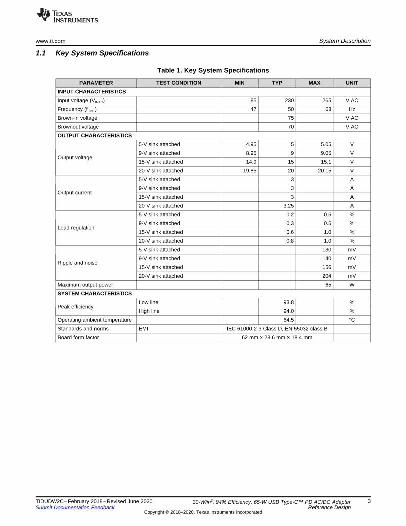
1.1 Key System Specifications
Table 1. Key System Specifications
PARAMETER TEST CONDITION MIN TYP MAX UNITINPUT CHARACTERISTICSInput voltage (VINAC) 85 230 265 V ACFrequency (fLINE) 47 50 63 HzBrown-in voltage 75 V ACBrownout voltage 70 V ACOUTPUT CHARACTERISTICS
Output voltage
5-V sink attached 4.95 5 5.05 V9-V sink attached 8.95 9 9.05 V15-V sink attached 14.9 15 15.1 V20-V sink attached 19.85 20 20.15 V
Output current
5-V sink attached 3 A9-V sink attached 3 A15-V sink attached 3 A20-V sink attached 3.25 A
Load regulation
5-V sink attached 0.2 0.5 %9-V sink attached 0.3 0.5 %15-V sink attached 0.6 1.0 %20-V sink attached 0.8 1.0 %
Ripple and noise
5-V sink attached 130 mV9-V sink attached 140 mV15-V sink attached 156 mV20-V sink attached 204 mV
Maximum output power 65 WSYSTEM CHARACTERISTICS
Peak efficiencyLow line 93.8 %High line 94.0 %
Operating ambient temperature 64.5 °CStandards and norms EMI IEC 61000-2-3 Class D, EN 55032 class BBoard form factor 62 mm × 28.6 mm × 18.4 mm

CSD17575
EMI &
Bridge
Rectifier
85~264
VAC
ISO7710F
UCC28780OPT
OATL431
UCC24612TPS25740B
TPD1E05U06
Vout
RTN
CC1/CC2
GAN
GAN
Q2
System Overview www.ti.com
4 TIDUDW2C–February 2018–Revised June 2020Submit Documentation Feedback
Copyright © 2018–2020, Texas Instruments Incorporated
30-W/in3, 94% Efficiency, 65-W USB Type-C™ PD AC/DC AdapterReference Design
2 System Overview
2.1 Block DiagramFigure 2 shows the high-level block diagram of the circuit. The main topology of this reference design isactive clamp flyback (ACF), which is controlled by TI’s new ACF controller UCC28780. The synchronizerectifier controller UCC24612-1 controls the synchronize rectifier MOSFET for better efficiencyperformance. The main switching devices are NV6115 and NV6117 GaN devices from NavitasSemiconductor, Inc. The TI USB-PD source controller TPS25740B controls the output fully compatiblewith the USB-PD 2.0 standard with 5-V/3-A, 9-V/3-A, 15-V/3-A, 20-V/3.25-A outputs.
Figure 2. Block Diagram of TIDA-01622
2.2 Highlighted Products
2.2.1 UCC28780The UCC28780 is a high-frequency active-clamp flyback controller that enables high-density AC/DC powersupplies that comply with stringent global efficiency standards. Zero voltage switching (ZVS) is achievedover wide operating range with an advanced auto-tuning technique, adaptive dead time optimization, andvariable switching frequency control law. Along with multimode control that changes the operation basedon input and output conditions, the UCC28780 controller enables high efficiency without the risk of audiblenoise. The controller has a variable switching frequency of up to 1 MHz and accurate programmable OPP,which provides consistent thermal design power across a wide line range. This consistent power meanspassive components can be further reduced and enable high power density.
Key features for this device include the following:• Configurable with external Si or GaN FETs• Adaptive burst control for light-load efficiency with low output ripple and no audible noise• Secondary-side regulation allows for dynamically scalable output voltage• Internal soft start• Brownout detection without direct line sensing• Fault protections: Internal overtemperature, output overvoltage, overcurrent, short circuit, and pin fault• NTC resistor interface with external enable

www.ti.com System Overview
5TIDUDW2C–February 2018–Revised June 2020Submit Documentation Feedback
Copyright © 2018–2020, Texas Instruments Incorporated
30-W/in3, 94% Efficiency, 65-W USB Type-C™ PD AC/DC AdapterReference Design
2.2.2 UCC24612The UCC24612 is a high-performance controller and driver for standard and logic-level N-channelMOSFET power devices used for low-voltage, secondary-side synchronous rectification. The combinationof controller and MOSFET emulates a near-ideal diode rectifier. This solution not only directly reducespower dissipation of the rectifier, but also indirectly reduces primary-side losses as well due tocompounding of efficiency gains. Using drain-to-source voltage sensing, the UCC24612 is ideal for ACFpower supplies. This device is available in a 5-pin SOT-23-5 package.
Key features for this device include the following:• Up to 1-MHz operating frequency• VDS MOSFET sensing• 4-A sink, 1-A source gate-drive capability• Micro-power sleep current for 90+ designs• Automatic light-load management• Synchronous wake-up from sleep and light-load modes• Adaptive minimum off time for better noise immunity• 16-ns typical turnoff propagation delay• 9.5-V gate drive clamp levels for minimum driving loss
2.2.3 TPS25740BWithout any firmware configuration, the TPS25740B implements a source that is certified for USB-PD 2.0version 1.2 and Type-C revision 1.2 designed to minimize time to market. The device offers four differentvoltages using USB-PD. The voltages and currents advertised are easily configured and the device canselect the voltage from the power supply based on the voltage requested by the attached sink. The deviceautomatically handles discharging the VBUS output per USB-PD requirements.
Key features for this device include the following:• Pin-selectable voltage advertisement:
– 5 V, 9 V, 12 V, and 15 V– 5 V, 9 V, 15 V, and 20 V
• Pin-selectable peak power settings:– Eight options 18 W to 100 W
• High voltage and safety integration:– OVP, OCP, OTP, and VBUS discharge– IEC 61000-4-2 protection on CC1 and CC2– Input pin for fast shutdown under fault– Control of external N-channel MOSFET– Three-pin external power supply control– Wide VIN supply: 4.65 V to 25 V
• Below 10-μA quiescent current when unattached• Port attachment indicator• Self-directed port power management for dual-port applications
2.2.4 ATL431The ATL431 is a three-terminal adjustable shunt regulator with specified thermal stability over applicableautomotive, commercial, and industrial temperature ranges. The output voltage can be set to any valuebetween VREF (approximately 2.5 V) and 36 V with two external resistors. The regulator has a typicaloutput impedance of 0.05 Ω. The operation current is as low as 35 µA (min), keeping the power loss at aquite low value.
System Overview www.ti.com
6 TIDUDW2C–February 2018–Revised June 2020Submit Documentation Feedback
Copyright © 2018–2020, Texas Instruments Incorporated
30-W/in3, 94% Efficiency, 65-W USB Type-C™ PD AC/DC AdapterReference Design
2.2.5 ISO7710The ISO7710 device is a high-performance, single-channel digital isolator with 5000-VRMS (DW package)and 3000-VRMS (D package) isolation ratings per UL 1577. This device is also certified by VDE, TUV, CSA,and CQC. The ISO7710 device provides high EMI and low emissions at a low power consumption whileisolating CMOS or LVCMOS digital I/Os. The isolation channel has a logic input and output bufferseparated by a silicon dioxide (SiO2) insulation barrier. In the event of input power or signal loss, defaultoutput is high for a device without suffix F and low for a device with suffix F.
2.2.6 CSD17578Q3AThe CSD17578Q3A is a 30-V NexFET™ Power MOSFET with a very low RDSon of 6.3 mΩ and a SON 3.3-mm×3.3-mm package. In this reference design, this device is used as a PD function switch for its low costand RDSon.
2.2.7 TPD1E05U06-Q1The TPD1E05U06-Q1 is a one-channel ESD protection diode for speeds up to 6 Gbps. The ultra-lowloading capacitance makes this device ideal for protecting any high-speed signal applications includingUSB 2.0 or 3.0, HDMI 1.4 or 2.0, SIM cards, and so on.
2.3 System Design TheoryThis reference design operates over a wide input voltage ranges from 85-V to 265-V AC and is fullycompatible with the USB-PD 2.0 standard with 5-V/3-A, 9-V/3-A, 15-V/3-A, and 20-V/3.25-A outputs. Thepower supply operates as ACF topology controlled by the UCC28780. And the output voltage is selectedby TPS25740B based on the voltage requested by the attached sink. The peak efficiency achieves 94% ata 230-V AC input and 93% at a 115-V AC input. The high switching frequency helps to decrease thetransformer and EMI filter size to achieve a high power density.
2.3.1 ACF Converter DesignACF is a two-switch topology that achieves soft switching and recovers leakage inductance energy.Compared with traditional ACF in continuous conduction mode (CCM), ACF in critical conduction mode(CrCM) uses the magnetizing inductance instead of leakage inductance to store ZVS energy. Asmagnetizing inductance is much larger than leakage inductance, only a small amount of negativemagnetizing current is required to achieve full ZVS soft switching. By controlling the amount of negativemagnetizing current, ZVS can easily be achieved from zero to full load. With proper design, the outputrectifier achieves zero current switching (ZCS) during turnoff. All these features make ACF successful athigh power density and efficiency adapter applications.
Table 2. ACF Design Goal Parameters
PARAMETER TEST CONDITION MIN TYP MAX UNITINPUT CHARACTERISTICSInput voltage (VINAC) 85 230 265 V ACBrown-in voltage 75 V ACBrownout voltage 70 V ACOUTPUT CHARACTERISTICSOutput voltage 5 20 VMaximum output power 65 WBurst mode load threshold 60 %
Peak efficiencyLow line 93.8 %High line 94.0 %
Load regulation 1.0 %

2 2max BIULK _ min
mSW _ min OUT _ max
D VL 79 H
2 f P
u u K P
u u
PS OUT _ maxmax
BULK _ min PS OUT _ max
N VD 0.67
V N V
u
� u
� �BULK _max
PS _mindera DS _ SR OUT _max spike
VN 4.68
1 K V V V
� u � �
� �dera DS _ GaN BULK _maxPS _max
OUT _max
1 K V VN 6.87
V
� u �
out _ maxhold _ up
2 2BULK _RUN Brownout
2 PT
CV V
uu
K
�
www.ti.com System Overview
7TIDUDW2C–February 2018–Revised June 2020Submit Documentation Feedback
Copyright © 2018–2020, Texas Instruments Incorporated
30-W/in3, 94% Efficiency, 65-W USB Type-C™ PD AC/DC AdapterReference Design
2.3.1.1 Bulk Capacitor CalculationThe minimum value of a bulk capacitor is determined by the hold-up time (Thold_up). A larger bulk capacitorvalue means a larger capacitor size; therefore, to maintain a high power density, the bulk capacitor valueis determined by the hold-up time.
(1)
Where:• POUT_max is the maximum output power• VBULK_RUN is the typical DC voltage on a bulk capacitor• VBrownout is the DC brownout voltage
2.3.1.2 Transformer Turns Ratio CalculationThe transformer turns ratio is determined by the voltage rating of GaN and synchronous rectificationMOSFET. The voltage stress of GaN NV6117 is 650 V and the SR MOSFET is a 150-V Si device.Therefore, the maximum and minimum turns ratio can be calculated separately using Equation 2 andEquation 3, respectively.
(2)
Where:• Kdera is the GaN voltage derating• VDS_GaN is the maximum GaN drain-to-source voltage rating• VBULK_max is the maximum bulk voltage• VOUT_max is the maximum output voltage
(3)
Where:• VDS_SR is the SR MOSFET drain-to-source voltage rating• Vspike is the spike voltage on SR MOSFET
A larger turns ratio means a larger main switch duty cycle and smaller secondary RMS current. In thisreference design, the turns ratio is designed as 6 to maintain the minimum secondary RMS current, whichdoes better to the efficiency and thermal.
2.3.1.3 Primary Magnetic Inductance CalculationAfter NPS is chosen, the primary magnetic inductance (Lm) can be determined based on the minimumswitching frequency (fSW_min) at the minimum bulk voltage (VBULK_min), maximum duty cycle (Dmax), andmaximum output power (POUT_max). When selecting the minimum switching, consider the impact on full-loadefficiency and EMI filter design.
Calculate the maximum duty cycle and primary inductance using Equation 4 and Equation 5.
(4)
(5)

SWm BULK _ min
m
Ci V
L� � u
OUT _ max 2m m
m SW _ min
2 Pi i
L f� �
u �
K u u
2m m
clamp _ maxk PS OUT _ min
2L i1C
L 3 N V�
uS u u
a2 _ max DD _ max
S
N 0.9V1.35
N 20
a2 _ min DD _ min
S
N 1.8V1.26
N 15
a1_ min DD _ min
S
N 1.8V3.78
N 5
NPNS
Na1
Na2
System Overview www.ti.com
8 TIDUDW2C–February 2018–Revised June 2020Submit Documentation Feedback
Copyright © 2018–2020, Texas Instruments Incorporated
30-W/in3, 94% Efficiency, 65-W USB Type-C™ PD AC/DC AdapterReference Design
2.3.1.4 Auxiliary-to-Secondary Turn Ratio DesignThe UCC28780 and both GaN devices are all powered by auxiliary winding at run mode. Two windingsare designed to make sure that VDD will not be lower than the turnoff voltage and to minimize the powerconsumption. Figure 3 shows the auxiliary power diagram.
Figure 3. Auxiliary Power Diagram
The Na1 winding is designed to power the devices at 5-V and 9-V outputs. Considering the voltagederating at a light load, there should be enough margin on VDD_min. Then at a 9-V output, the VDD is equalto the TVS diode voltage of 18 V. Na1 must stay a small value to decrease the power consumption on thetransistor.
The Na2 winding is designed to power the devices at 15-V and 20-V outputs. Calculate the auxiliary-to-secondary turn ratio using Equation 6, Equation 7, and Equation 8.
(6)
(7)
(8)
2.3.1.5 Clamp Capacitor CalculationConsider the design trade-off between conduction loss reduction and turnoff switching loss of the high-side switching device (QH). A higher clamp capacitor (Cclamp) results in less RMS current flowing throughthe transformer windings and switching devices; therefore, the conduction loss can be reduced. However,a higher Cclamp design results in QH turning off before the clamp current returns to zero. The condition ofnon-ZCS increases the turnoff switching loss of QH. Therefore, Cclamp needs to be fine tuned based on theloss attribution. For best results, design the resonance between leakage inductance (Lk) and Cclamp to becompleted by the time between resonant current is zero and QH is turned off. In this setup, thedemagnetization time must be equal to around three quarters of the resonant period. Use Equation 9,Equation 10, and Equation 11 to design Cclamp for obtaining ZCS at a minimum bulk voltage, minimumoutput voltage, and full load. A low-ESR clamp capacitor is required to minimize the conduction loss.
(9)
(10)
(11)

� �max SW _ min m SW pk pk
Co _ maxOUT _ max
2 1 D f L C VR
I
�� � u Su u
S u
load transOUT _ min
trans _ max
I tC
V
' u '
'
� � kresidual max_ QH max_ SR
clamp
LV min i , i
C u
FDRBleed
PS OUT _ maxclamp
residual
tR
N VC ln
V
u§ ·
¨ ¸© ¹
www.ti.com System Overview
9TIDUDW2C–February 2018–Revised June 2020Submit Documentation Feedback
Copyright © 2018–2020, Texas Instruments Incorporated
30-W/in3, 94% Efficiency, 65-W USB Type-C™ PD AC/DC AdapterReference Design
2.3.1.6 Bleed Resistor CalculationA large bleed resistor (RBleed) is used to discharge clamp capacitor voltage to a residual voltage (Vresidual)during the 1.44-s fault delay recovery time (tFDR). After the converter recovers from the fault mode, thelower Vresidual reduces the maximum current flowing through QH and SR within their respective safeoperating areas, even if the output voltage is shorted. The target Vresidual can be calculated based on themaximum pulse current of QH or the SR current reflected to the primary side, depending on which is lower.
(12)
2.3.1.7 Output Capacitor CalculationOutput capacitance (COUT) is determined by evaluating several factors and choosing the largest of theresults.1. The minimum output capacitor value must be enough to meet transient specification of output voltage
due to a given load step until the voltage-control loop can respond to restore regulation.Where:• ΔIload is maximum load-step magnitude for transient response• ΔVtrans_max is the maximum transient voltage deviation for transient response• Δttrans is the transient response time
2. The maximum ESR of output capacitor is often limited by the maximum output peak-to-peak voltageripple (Vpk-pk), where the worst-case output ripple is considered at maximum load (IOUT_max). If the high-frequency switching ripple at the output is mainly dominated by the ESR ripple, a sinusoidalapproximation of the secondary current waveform of the ACF is made to calculate the ESRrequirement based on the target output ripple specification.
(13)
(14)
(15)
2.3.2 USB-PD DesignThe USB-PD source controller TPS25740B is used in this reference design to achieve USB-PD 2.0functions. The device can control an external voltage regulator by three digital PINs (CTL1, CTL2, andCTL3) to select the voltage from the power supply based on the voltage requested by the attached sink.Table 3 summarizes the control relationship between the CTL1, CTL2, and CTL3 statuses and VBUS.
Table 3. PD Control Relationship
VOLTAGE CONTAINED IN PDO REQUESTED BY UFP CTL3 STATE CTL2 STATE CLT1 STATE5 V High-z High-z High-z9 V High-z Low High-z15 V High-z Low Low20 V Low Low Low

� �REF
CTL3
REF REF REF REF
D1 D2 CTL2 CTL1
VR
15 V V V V V
R R R R
�
� � �
� �REF
CTL1
REF REF REF
D1 D2 CTL2
VR
15 V V V V
R R R
�
� �
� �REF
CTL2
REF REF
D1 D2
VR
9 V V V
R R
�
�
System Overview www.ti.com
10 TIDUDW2C–February 2018–Revised June 2020Submit Documentation Feedback
Copyright © 2018–2020, Texas Instruments Incorporated
30-W/in3, 94% Efficiency, 65-W USB Type-C™ PD AC/DC AdapterReference Design
The USB-PD control resistors can be calculated from Equation 16, Equation 17, and Equation 18 basedon Table 3.
(16)
(17)
(18)
www.ti.com Hardware, Software, Testing Requirements, and Test Results
11TIDUDW2C–February 2018–Revised June 2020Submit Documentation Feedback
Copyright © 2018–2020, Texas Instruments Incorporated
30-W/in3, 94% Efficiency, 65-W USB Type-C™ PD AC/DC AdapterReference Design
3 Hardware, Software, Testing Requirements, and Test Results
3.1 Required Hardware and Software
3.1.1 Hardware• Isolated AC source• Single-phase power analyzer• Digital oscilloscope• Multimeters• Electronic load• USB Type-C™ UFP Load Board PMP20413
3.2 Testing and Results
3.2.1 Test Setup1. Connect input terminals of the reference board to the AC power source.2. Connect output terminals to the PMP20413 input terminals.3. Connect the PMP20413 output terminals to electronic load, maintaining correct polarity.4. Set a minimum load of about 0 A and minimum voltage of 25 V.5. Gradually increase the input voltage from 0 V to turn on voltage of 75-V AC.6. Observe that the output voltage across the load terminals has risen to about 5 V.7. Increase the load to maximum load smoothly and observe the switching waveforms.8. Select different output voltages through the PMP20413 device.9. Increase the load to maximum load smoothly and observe the switching waveforms.10. Compare these results with those presented in the design guide.
3.2.2 Test Results
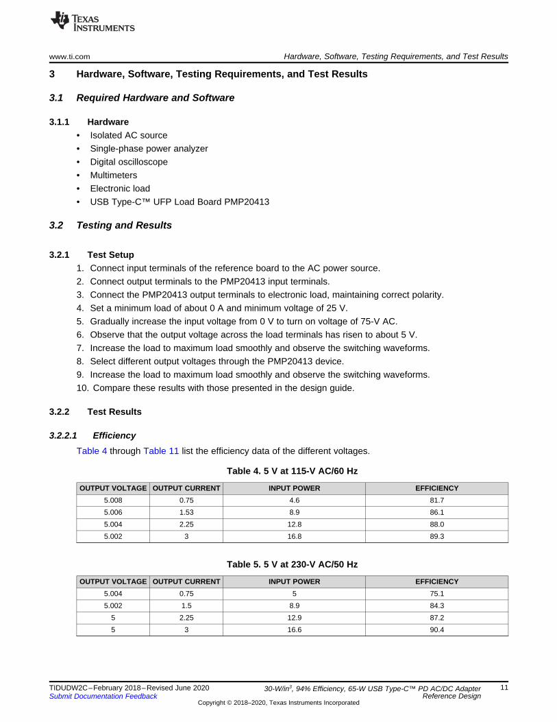
3.2.2.1 EfficiencyTable 4 through Table 11 list the efficiency data of the different voltages.
Table 4. 5 V at 115-V AC/60 Hz
OUTPUT VOLTAGE OUTPUT CURRENT INPUT POWER EFFICIENCY5.008 0.75 4.6 81.75.006 1.53 8.9 86.15.004 2.25 12.8 88.05.002 3 16.8 89.3
Table 5. 5 V at 230-V AC/50 Hz
OUTPUT VOLTAGE OUTPUT CURRENT INPUT POWER EFFICIENCY5.004 0.75 5 75.15.002 1.5 8.9 84.3
5 2.25 12.9 87.25 3 16.6 90.4

Hardware, Software, Testing Requirements, and Test Results www.ti.com
12 TIDUDW2C–February 2018–Revised June 2020Submit Documentation Feedback
Copyright © 2018–2020, Texas Instruments Incorporated
30-W/in3, 94% Efficiency, 65-W USB Type-C™ PD AC/DC AdapterReference Design
Table 6. 9 V at 115-V AC/60 Hz
OUTPUT VOLTAGE OUTPUT CURRENT INPUT POWER EFFICIENCY9.02 0.75 8 84.69.02 1.5 15 90.29.02 2.25 22 92.39.01 3 29 93.2
Table 7. 9 V at 230-V AC/50 Hz
OUTPUT VOLTAGE OUTPUT CURRENT INPUT POWER EFFICIENCY9.02 0.75 8.1 83.59.01 1.5 15.3 88.39.01 2.25 22.4 90.59.01 3 29 93.2
Table 8. 15 V at 115-V AC/60 Hz
OUTPUT VOLTAGE OUTPUT CURRENT INPUT POWER EFFICIENCY14.99 0.75 12.5 89.914.99 1.5 24.3 92.514.98 2.25 36.2 93.114.98 3 47.9 93.8
Table 9. 15 V at 230-V AC/50 Hz
OUTPUT VOLTAGE OUTPUT CURRENT INPUT POWER EFFICIENCY14.98 0.75 12.7 88.514.97 1.5 24.6 91.314.96 2.25 36.55 92.114.96 3 47.9 93.7
Table 10. 20 V at 115-V AC/60 Hz
OUTPUT VOLTAGE OUTPUT CURRENT INPUT POWER EFFICIENCY19.85 0.82 17.8 91.419.84 1.63 34.9 92.719.83 2.44 51.8 93.419.83 3.25 68.9 93.5
Table 11. 20 V at 230-V AC/50 Hz
OUTPUT VOLTAGE OUTPUT CURRENT INPUT POWER EFFICIENCY19.83 0.82 18.1 89.819.81 1.63 35.3 91.519.8 2.44 52 92.919.8 3.25 68.5 94.0

Load
Outp
ut V
oltage
0.0 0.1 0.2 0.3 0.4 0.5 0.6 0.7 0.8 0.9 1.00
5
10
15
20
25
D003
5 V9 V
15 V20 V
Load
Effic
ien
cy (�
)
0.25 0.35 0.45 0.55 0.65 0.75 0.85 0.9574
76
78
80
82
84
86
88
90
92
94
D005
5 VOUT
9 VOUT
15 VOUT
20 VOUT
Load
Effic
ien
cy (�
)
0.25 0.35 0.45 0.55 0.65 0.75 0.85 0.9581.5
82.5
83.5
84.5
85.5
86.5
87.5
88.5
89.5
90.5
91.5
92.5
93.5
D004
5 VOUT
9 VOUT
15 VOUT
20 VOUT
www.ti.com Hardware, Software, Testing Requirements, and Test Results
13TIDUDW2C–February 2018–Revised June 2020Submit Documentation Feedback
Copyright © 2018–2020, Texas Instruments Incorporated
30-W/in3, 94% Efficiency, 65-W USB Type-C™ PD AC/DC AdapterReference Design
Figure 4 and Figure 5 show the efficiency curves.
Figure 4. Efficiency Curve at 115-V AC Figure 5. Efficiency Curve at 230-V AC
3.2.2.2 Standby Power Loss
Table 12. Standby Power Loss
VinTIDA-01622
INPUT POWER LOSS CoC V5 TIER 2 DOE_VI
115-V AC/60 Hz 35 mW75 mW 150 mW
230-V AC/50 Hz 45 mW
3.2.2.3 Load RegulationFigure 6 shows the load regulation at 115-V AC/60 Hz.
Figure 6. Load Regulation

Hardware, Software, Testing Requirements, and Test Results www.ti.com
14 TIDUDW2C–February 2018–Revised June 2020Submit Documentation Feedback
Copyright © 2018–2020, Texas Instruments Incorporated
30-W/in3, 94% Efficiency, 65-W USB Type-C™ PD AC/DC AdapterReference Design
3.2.2.4 Output Voltage Transitions
3.2.2.4.1 Start-up
Figure 7. Start-up Waveform at 115-V AC and No Load
3.2.2.4.2 5 V to 9 V
Figure 8. 5-V to 9-V Transition at 115-V AC and No Load

www.ti.com Hardware, Software, Testing Requirements, and Test Results
15TIDUDW2C–February 2018–Revised June 2020Submit Documentation Feedback
Copyright © 2018–2020, Texas Instruments Incorporated
30-W/in3, 94% Efficiency, 65-W USB Type-C™ PD AC/DC AdapterReference Design
3.2.2.4.3 9 V at 15 V
Figure 9. 9-V to 15-V Transition at 115-V AC and No Load
3.2.2.4.4 15 V to 20 V
Figure 10. 15-V to 20-V Transition at 115-V AC and No Load
Hardware, Software, Testing Requirements, and Test Results www.ti.com
16 TIDUDW2C–February 2018–Revised June 2020Submit Documentation Feedback
Copyright © 2018–2020, Texas Instruments Incorporated
30-W/in3, 94% Efficiency, 65-W USB Type-C™ PD AC/DC AdapterReference Design
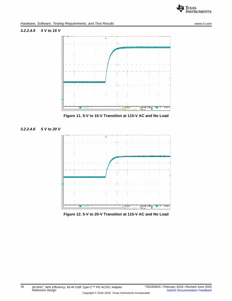
3.2.2.4.5 5 V to 15 V
Figure 11. 5-V to 15-V Transition at 115-V AC and No Load
3.2.2.4.6 5 V to 20 V
Figure 12. 5-V to 20-V Transition at 115-V AC and No Load

www.ti.com Hardware, Software, Testing Requirements, and Test Results
17TIDUDW2C–February 2018–Revised June 2020Submit Documentation Feedback
Copyright © 2018–2020, Texas Instruments Incorporated
30-W/in3, 94% Efficiency, 65-W USB Type-C™ PD AC/DC AdapterReference Design
3.2.2.4.7 9 V to 20 V
Figure 13. 9-V to 20-V Transition at 115-V AC and No Load
3.2.2.5 Output Voltage Ripple
Figure 14. 115-V AC/60-Hz Input, 5-V/3-A Output
Hardware, Software, Testing Requirements, and Test Results www.ti.com
18 TIDUDW2C–February 2018–Revised June 2020Submit Documentation Feedback
Copyright © 2018–2020, Texas Instruments Incorporated
30-W/in3, 94% Efficiency, 65-W USB Type-C™ PD AC/DC AdapterReference Design
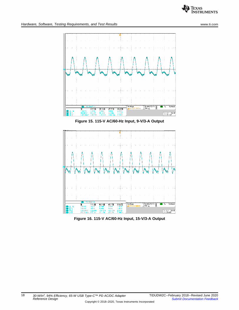
Figure 15. 115-V AC/60-Hz Input, 9-V/3-A Output
Figure 16. 115-V AC/60-Hz Input, 15-V/3-A Output

www.ti.com Hardware, Software, Testing Requirements, and Test Results
19TIDUDW2C–February 2018–Revised June 2020Submit Documentation Feedback
Copyright © 2018–2020, Texas Instruments Incorporated
30-W/in3, 94% Efficiency, 65-W USB Type-C™ PD AC/DC AdapterReference Design
Figure 17. 115-V AC/60-Hz Input, 20-V/3.25-A Output
3.2.2.6 Loop Gain
Figure 18. Loop Gain at 115-V AC/60-Hz Input, 20-V/3.25-A Output

Hardware, Software, Testing Requirements, and Test Results www.ti.com
20 TIDUDW2C–February 2018–Revised June 2020Submit Documentation Feedback
Copyright © 2018–2020, Texas Instruments Incorporated
30-W/in3, 94% Efficiency, 65-W USB Type-C™ PD AC/DC AdapterReference Design
Figure 19. Loop Gain at 230-V AC/50-Hz Input, 20-V/3.25-A Output
3.2.2.7 CE Test Results
Figure 20. 115-V AC Input, 20-V/3.25-A Output
Table 13. Final Result for 115-V AC Input, 20-V/3.25-A Output
FREQ(MHz)
QUASIPEAK(dBµV)
AVERAGE(dBµV)
LIMIT(dBµV)
MARGIN(dB)
MEAS TIME(ms)
BANDWIDTH(kHz) LINE FILTER CORR
(dB)0.280500 51.81 — 60.80 8.99 1000.0 9.000 L1 ON 19.62.483250 46.66 — 56.00 9.34 1000.0 9.000 L1 ON 19.63.099750 48.25 — 56.00 7.75 1000.0 9.000 L1 ON 19.63.653250 48.39 — 56.00 7.61 1000.0 9.000 L1 ON 19.6

www.ti.com Hardware, Software, Testing Requirements, and Test Results
21TIDUDW2C–February 2018–Revised June 2020Submit Documentation Feedback
Copyright © 2018–2020, Texas Instruments Incorporated
30-W/in3, 94% Efficiency, 65-W USB Type-C™ PD AC/DC AdapterReference Design
Figure 21. 230-V AC Input, 20-V/3.25-A Output
Table 14. Final Result for 230-V AC Input, 20-V/3.25-A Output
FREQ(MHz)
QUASIPEAK(dBµV)
AVERAGE(dBµV)
LIMIT(dBµV)
MARGIN(dB)
MEAS TIME(ms)
BANDWIDTH(kHz) LINE FILTER CORR
(dB)0.368250 — 41.30 48.54 7.24 1000.0 9.000 N ON 19.60.370500 48.52 — 58.49 9.97 1000.0 9.000 N ON 19.60.737250 — 45.21 46.00 0.79 1000.0 9.000 N ON 19.60.739500 53.59 — 56.00 2.41 1000.0 9.000 N ON 19.61.106250 — 42.36 46.00 3.64 1000.0 9.000 N ON 19.61.844250 — 40.59 46.00 5.41 1000.0 9.000 N ON 19.61.844250 53.44 — 56.00 2.56 1000.0 9.000 N ON 19.62.215500 — 40.21 46.00 5.79 1000.0 9.000 N ON 19.62.217750 52.50 — 56.00 3.50 1000.0 9.000 N ON 19.6
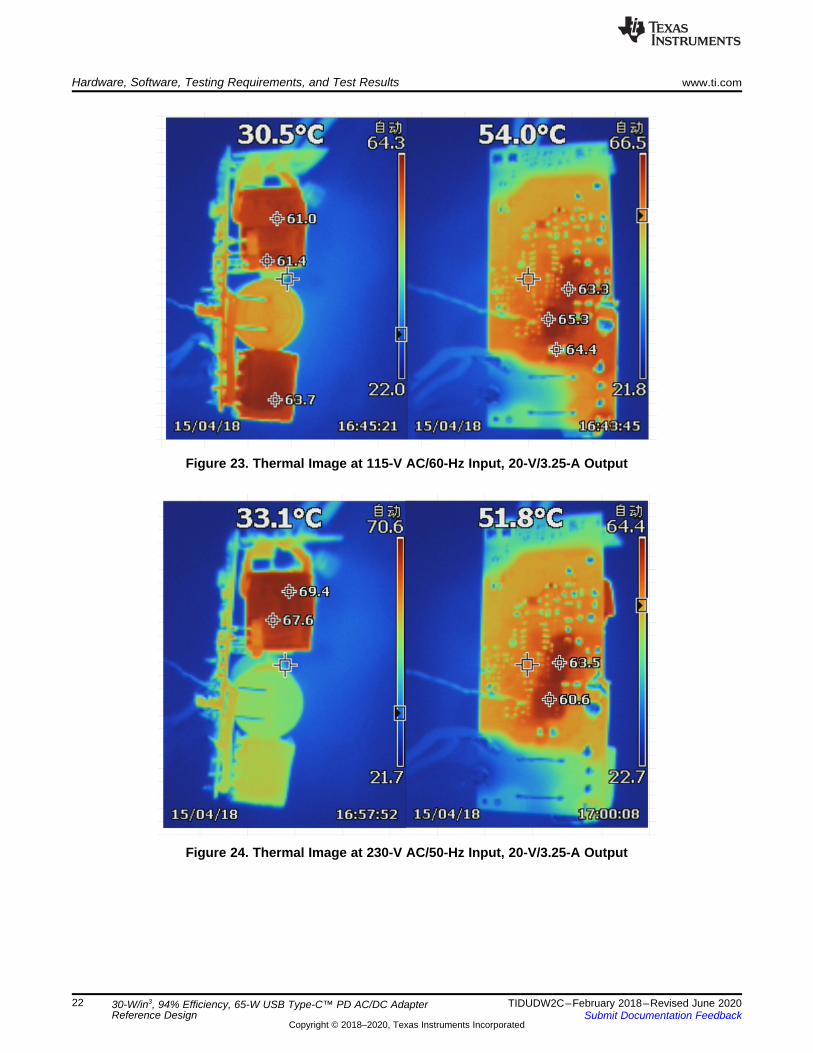
3.2.2.8 Thermal Image
Figure 22. Thermal Image at 90-V AC/60-Hz Input, 20-V/3.25-A Output
Hardware, Software, Testing Requirements, and Test Results www.ti.com
22 TIDUDW2C–February 2018–Revised June 2020Submit Documentation Feedback
Copyright © 2018–2020, Texas Instruments Incorporated
30-W/in3, 94% Efficiency, 65-W USB Type-C™ PD AC/DC AdapterReference Design
Figure 23. Thermal Image at 115-V AC/60-Hz Input, 20-V/3.25-A Output
Figure 24. Thermal Image at 230-V AC/50-Hz Input, 20-V/3.25-A Output

www.ti.com Hardware, Software, Testing Requirements, and Test Results
23TIDUDW2C–February 2018–Revised June 2020Submit Documentation Feedback
Copyright © 2018–2020, Texas Instruments Incorporated
30-W/in3, 94% Efficiency, 65-W USB Type-C™ PD AC/DC AdapterReference Design
Figure 25. Thermal Image at 265-V AC/50-Hz Input, 20-V/3.25-A Output

Design Files www.ti.com
24 TIDUDW2C–February 2018–Revised June 2020Submit Documentation Feedback
Copyright © 2018–2020, Texas Instruments Incorporated
Revision History
4 Design Files
4.1 SchematicsTo download the schematics, see the design files at TIDA-01622.
4.2 Bill of MaterialsTo download the bill of materials (BOM), see the design files at TIDA-01622.
4.3 PCB Layout Recommendations
4.3.1 Layout PrintsTo download the layer plots, see the design files at TIDA-01622.
4.4 Altium ProjectTo download the Altium project files, see the design files at TIDA-01622.
4.5 Gerber FilesTo download the Gerber files, see the design files at TIDA-01622.
4.6 Assembly DrawingsTo download the assembly drawings, see the design files at TIDA-01622.
5 Software FilesTo download the software files, see the design files at TIDA-01622.
6 Related DocumentationThis reference design did not use any documentation.
6.1 TrademarksTI E2E, NexFET are trademarks of Texas Instruments.USB Type-C is a trademark of USB Implementers Forum, Inc.All other trademarks are the property of their respective owners.
Revision HistoryNOTE: Page numbers for previous revisions may differ from page numbers in the current version.
Changes from B Revision (April 2019) to C Revision .................................................................................................... Page
• Changed block diagram .................................................................................................................. 1
Changes from A Revision (August 2018) to B Revision ................................................................................................ Page
• Added notebook PC power adapter design, mobile wall charger design, and other AC/DC adapters/PSU to Applications 1
Changes from Original (February 2018) to A Revision .................................................................................................. Page
• Changed peak efficiency from 92% to 94% in design title........................................................................... 1• Changed 20 mm to 18.4 mm in ......................................................................................................... 1• Added Table 4............................................................................................................................ 11

www.ti.com Revision History
25TIDUDW2C–February 2018–Revised June 2020Submit Documentation Feedback
Copyright © 2018–2020, Texas Instruments Incorporated
Revision History
• Added Table 5............................................................................................................................ 11• Added Table 6............................................................................................................................ 11• Added Table 7............................................................................................................................ 11• Added Table 8............................................................................................................................ 11• Added Table 9............................................................................................................................ 11• Added Table 10 .......................................................................................................................... 11• Added Table 11 .......................................................................................................................... 11• Added Table 12 .......................................................................................................................... 13• Changed Figure 4........................................................................................................................ 13• Changed Figure 5........................................................................................................................ 13• Added Figure 18 ......................................................................................................................... 19• Added Figure 19 ......................................................................................................................... 20• Changed Figure 22 ...................................................................................................................... 21• Added Figure 23 ......................................................................................................................... 22• Added Figure 24 ......................................................................................................................... 22• Added Figure 25 ......................................................................................................................... 23

IMPORTANT NOTICE AND DISCLAIMER
TI PROVIDES TECHNICAL AND RELIABILITY DATA (INCLUDING DATASHEETS), DESIGN RESOURCES (INCLUDING REFERENCE DESIGNS), APPLICATION OR OTHER DESIGN ADVICE, WEB TOOLS, SAFETY INFORMATION, AND OTHER RESOURCES “AS IS” AND WITH ALL FAULTS, AND DISCLAIMS ALL WARRANTIES, EXPRESS AND IMPLIED, INCLUDING WITHOUT LIMITATION ANY IMPLIED WARRANTIES OF MERCHANTABILITY, FITNESS FOR A PARTICULAR PURPOSE OR NON-INFRINGEMENT OF THIRD PARTY INTELLECTUAL PROPERTY RIGHTS.These resources are intended for skilled developers designing with TI products. You are solely responsible for (1) selecting the appropriate TI products for your application, (2) designing, validating and testing your application, and (3) ensuring your application meets applicable standards, and any other safety, security, or other requirements. These resources are subject to change without notice. TI grants you permission to use these resources only for development of an application that uses the TI products described in the resource. Other reproduction and display of these resources is prohibited. No license is granted to any other TI intellectual property right or to any third party intellectual property right. TI disclaims responsibility for, and you will fully indemnify TI and its representatives against, any claims, damages, costs, losses, and liabilities arising out of your use of these resources.TI’s products are provided subject to TI’s Terms of Sale (www.ti.com/legal/termsofsale.html) or other applicable terms available either on ti.com or provided in conjunction with such TI products. TI’s provision of these resources does not expand or otherwise alter TI’s applicable warranties or warranty disclaimers for TI products.
Mailing Address: Texas Instruments, Post Office Box 655303, Dallas, Texas 75265Copyright © 2020, Texas Instruments Incorporated