310z -2 fm exciter -...
TRANSCRIPT

523-0563912-001431 1 February 1975
e Rockwell International
Collins instruction book
310Z -2 FM Exciter Broadcast Division Collins Radio Group Rockwell International Dallas, Texas 75207
Printed in United States of America
www.americanradiohistory.com


table of contents
Page
Section 1 General Description 1 -1
1. 1 Introduction 1 -1 1.2 Physical Description 1 -1 1. 3 Functional Description 1 -1 1.4 Optional Equipment 1 -2 1.5 Technical Characteristics 1 -2 1.5.1 General 1 -2 1. 5, 2 Monaural FM 1 -3 1. 5.3 Stereo FM With 786V -1 1 -4 1. 5.4 SCA FM With 786W -1 1 -4 1. 5. 5 Composite Stereo STL With 785E -1 1 -5
Section 2 Installation 2 -1
2.1 General 2 -1 2.2 Preinstallation 2 -1 2.3 Wiring 2 -1 2. 3. 1 Audio Input Connections 2 -1 2.3.2 Stereo Remote Control 2 -3 2. 3.3 RF Output 2 -3 2.3.4 Input Power 2 -3 2.3.5 Power Control Override 2 -3 2.4 Initial Checks 2 -3 2.5 Output Frequency Change 2 -3
Section 3 Operation 3 -1
3.1 General 3 -1 3.2 Normal Turn -On Procedure 3 -1 3. 3 Alternate Turn -On Procedure 3 -1 3.4 Stereo /Monaural Remote Switching 3 -1
Section 4 Theory of Operation 4 -1
4.1 General 4 -1 4.2 Block Diagram Discussion 4 -1 4. 3 Stereo Generator A2 4 -2 4.3.1 Signals Required 4 -2 4. 3.2 Method of Signal Generation in 786V -1
Stereo Generator 4 -2 4. 3.3 Analysis of Signals Generated 4 -6 4.3.4 Circuit Analysis 4 -8
i
www.americanradiohistory.com

table of contents (cont)
Page
4.4 SCA Generator Al /A2 4 -9 4.4.1 General 4 -9 4.4.2 Circuit Analysis 4 -9 4.5 FM Modulator A4 4 -10 4.6 Audio /Regulator Card A7 4 -12 4.7 785E -1 STL Interface Card A3 4 -12 4.8 RF Amplifier A5 4 -13 4.9 Power Supplies 4 -13 4. 10 Meter Amplifier 4 -14
Section 5 Maintenance 5 -1
5.1 General 5 -1 5.2 Cleaning 5 -1 5.3 Lubrication 5 -2 5.4 Inspection 5 -2 5.5 Test Equipment Required 5 -2 5.6 Alignment and Adjustment 5 -3 5.6. 1 Power Supply Checks and Adjustments 5 -3 5. 6.2 Modulator Tests 5 -3 5.6.3 Audio Adjustments - Preemphasis Tracking
and Linear Crosstalk 5 -7 5. 6.4 SCA Generator Output Level Adjustment 5 -8 5.6.5 SCA Generator Frequency Adjustment 5 -8 5. 6. 6 Stereo Generator Adjustment 5 -8 5.7 Minimum Performance Standards 5 -9 5. 7. 1 Output Frequency 5 -9 5.7.2 Output Power 5 -9 5.7.3 FM Noise 5 -9 5.7.4 Frequency Response (Monaural) 5 -10 5.7. 5 Harmonic Distortion (Monaural) 5 -11 5.7. 6 Frequency Response (Stereo) 5 -11 5.7.7 Harmonic Distortion (Stereo) 5 -11 5.7.8 Subcarrier Suppression 5 -12 5.7.9 Channel Separation 5 -12 5.7.10 Main Channel to Subchannel Nonlinear
Crosstalk 5 -13 5.7. 11 Subchannel to Main Channel Nonlinear
Crosstalk 5 -14 5.7. 12 SCA Input Test 5 -14 5.7. 13 SCA Noise Test 5 -16 5.7. 14 SCA Mute Circuit Test 5 -16 5.7. 15 SCA Frequency Response 5 -17 5.8 Frequency Change 5 -17
ii
www.americanradiohistory.com

Section 6 Parts List
table of contents (cont)
Page
6 -1
6.1 General 6 -1 6.2 Ordering Replacement Parts 6 -1
Section 7 Diagrams 7 -1
list of illustrations
Figure Page
1 -1 310Z-2 FM Broadcast Exciter 1 -0 2 -1 310Z -2 FM Exciter, Outline Dimensions and
Installation Details 2 -2 3 -1 310Z -2 FM Exciter, Front Panel Controls and
Indicators 3-2 4 -1 310Z -2 FM Exciter, Simplified Block Diagram 4 -3 4 -2 Spectrum of Signals in Stereo Baseband Audio 4 -5 4 -3 Elementary Time -Division Multiplex System 4 -5 4 -4 Balanced Modulator Output When L + R = 2;
L -R =0 4 -7 4 -5 Balanced Modulator Output When L + R = 1;
L -R =1 4 -7 4 -6 Balanced Modulator Output When L + R = 0;
L -R =2 4 -8 5 -1 310Z -2 FM Exciter, Maintenance Controls 5 -4 5 -2 Test Equipment Connections to 310Z -2 for
Adjustment and Test Procedures 5 -6 5 -3 Stereo Test Circuit, Schematic Diagram 5 -7 5 -4 Test Equipment Connections to 310Z -2 for
Crosstalk Test 5 -14 5 -5 Nonlinear Crosstalk Test Circuit, Schematic
Diagram 5 -15 6 -1 310Z -2 FM Exciter (Sheet 1 of 3) 6 -2
iii
www.americanradiohistory.com
list of illustrations (cont)
Figure Page
6 -2 310Z -2 FM Exciter (Sheet 2 of 3) 6 -3 6 -3 310Z -2 FM Exciter (Sheet 3 of 3) 6 -4 6 -4 Extender Board 6 -7 6 -5 SCA Generator 786W -1 Al, A2 6 -9 6 -6 STL Interface 785E -1 A3 6 -13 6 -7 Stereo Generator 786V -1 A3 6 -15 6 -8 Modulator /Exciter A4 (Sheet 1 of 2) 6 -18 6 -9 Modulator /Exciter A4 (Sheet 2 of 2) 6 -19 6 -10 Power Amplifier AS 6 -23 6 -11 Audio /Mtr Regulator A6 6 -25 7 -1 310Z-2 FM Exciter, Detail Block Diagram 7 -3 7 -2 310Z-2 FM Exciter Main Frame, Schematic
Diagram 7 -5 7 -3 786W -1 SCA Generators Al /A2, Schematic
Diagram 7 -9 7 -4 786V -1 Stereo Generator A3, Schematic
Diagram 7 -11 7 -5 FM Modulator A4, Schematic Diagram 7 -13 7 -6 RF Amplifier A5, Schematic Diagram 7 -15 7 -7 785E -1 STL Interface Card A3, Schematic
Diagram 7 -16
list of tables
Table
1 -1 310Z -2 FM Exciter Special Features and
Page
Customer Options 1 -3 3 -1 310Z -2 FM Broadcast Exciter, Front Panel
Controls and Indicators 3 -3 3 -2 Test Meter Indications 3 -3 5 -1 Required Test Equipment 5 -2 5 -2 Maintenance Controls 5 -5 5 -3 Tests 5 -10 5 -4 Crystal Part Number 5 -18
iv
www.americanradiohistory.com

general description
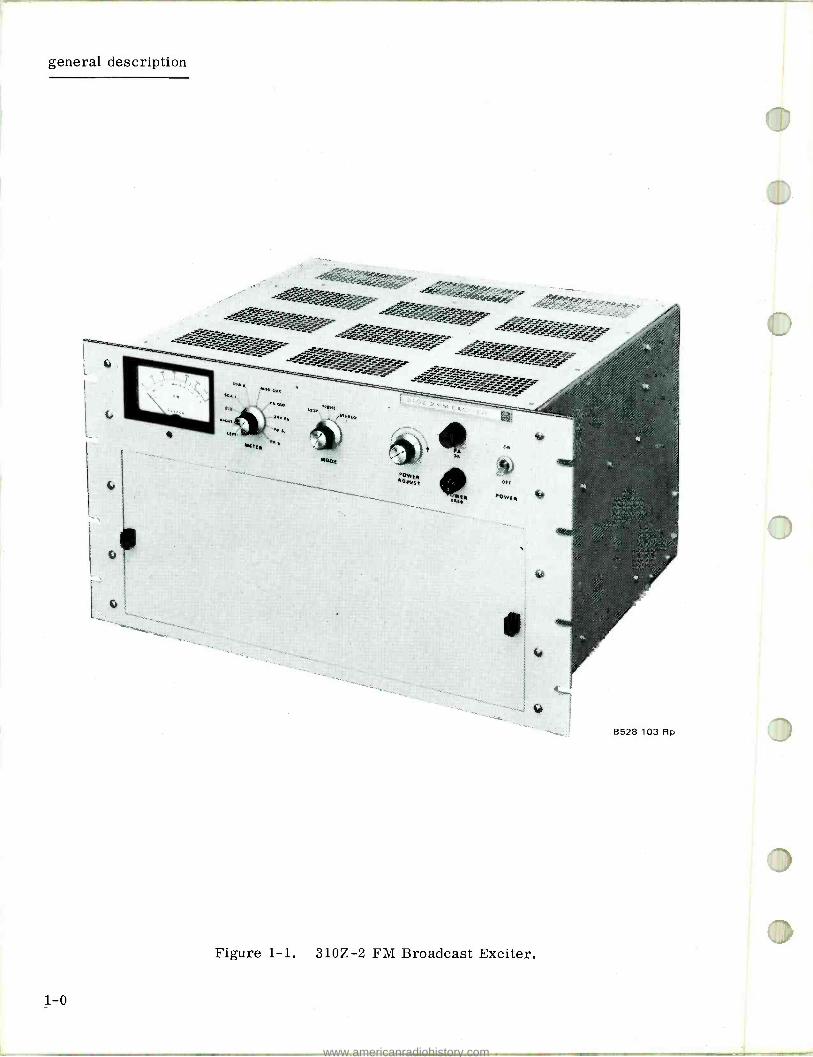
Figure 1 -1. 310Z -2 FM Broadcast Exciter.
1 -0
www.americanradiohistory.com

Section 1
General Description
1.1 IN TRODUCTION
The solid -state 310Z -2 FM broadcast exciter (figure 1 -1) provides a frequency -modulated signal in the 88- to 108 -MHz range (exact frequency as specified by the customer) for further amplification and transmission. The exciter can be adjusted manually to provide maximum output of 20 watts and is prewired to accept three optional plug -in modules. The optional 786W -1 SCA Generators enable background music to be transmitted at either 41 kHz or 67 kHz multiplexed on an FM broadcast. The optional 786V -1 Stereo Generator allows broadcasting compatible time -division multiplex stereo. In addition, the optional 785E -1 STL (studio transmitter link) Interface Card can be substituted for the 786V -1 Stereo Generator to interface the 310Z -2 with common composite STL systems or other systems requiring an external baseband input to the modulator.
1.2 PHYSICAL DESCRIPTION
The 310Z -2 exciter is 483 mm (19 in.) wide, 267 mm (10.5 in.) high, and 381 mm (15 in.) deep, weighs approximately 18 kg (40 lb) and is designed for mounting a standard 483 -mm (19 -in.) equipment rack. Controls and power supply components are mounted on the chassis. A card cage secured to the chassis provides receptacles for the five plug -in circuit cards that contain most of the circuits. A removable front panel provides access to the cards. Connectors for the rf signal output and for the ac power input as well as the terminal strip for audio inputs are located on the back of the exciter. Built -in shielding prevents radiation and interference.
1.3 FUNCTIONAL DESCRIPTION
The functional units of the 310Z -2 FM Exciter are an FM modulator and an rf amplifier. In addition, a stereo generator and one or two sca (subsidiary communication authorization) generators are optional units that may be included as part of the 310Z -2. Each of these major functional units is constructed as a plug -in module, and the 310Z -2 is prewired so that the stereo generator and the sca generator plug -in modules can be added at any time.
When the 310Z -2 is used only for monaural broadcasts (without the optional sca generators or stereo generator), the audio input is applied to the baseband input of the FM modulator through the required audio processing circuits. A carrier frequency oscillator is modulated to full deviation by the input. This FM signal is also applied to the AFC system, which maintains the oscillator output frequency at carrier frequency.
When the stereo generator is used, the exciter functions the same as described above with the exception that left and right audio inputs are applied to the stereo generator through separate preemphasis networks. These audio signals are multiplexed to provide the base - band signal, which is filtered and applied to the FM modulator. When an sca generator is used, the sca audio input is amplified and used to frequency- modulate a 41- or 67 -kHz subcarrier oscillator. The FM sca output is filtered and applied to the FM modulator.
1 -1
www.americanradiohistory.com

general description
1.4 OPTIONAL EQUIPMENT
The 786V -1 Stereo Generator, 785E -1 STL Interface Card, and 786W -1 SCA Generators are customer options. Table 1 -1 lists several 310Z -2 FM exciter features and indicates optional modules or cards required for each feature.
1.5 TECHNICAL CHARACTERISTICS
The technical characteristics for the 310Z -2 are listed below, and have been divided into five groups: (1) generator characteristics that apply to all 310Z-2 exciters, (2) those charac- teristics that apply to the 310Z -2 when it is used for monaural FM, (3) those characteristics that apply to the 310Z -2 when it is used for stereo FM with the 786V -1 Stereo Generator, (4) those characteristics that apply to the 310Z -2 when it is used for sca transmission with the 786W -1 SCA Generator, and (5) those characteristics that apply to the 310Z -2 when it is used for composite stereo STL transmission with the 785E -1 STL Interface Card.
1.5.1 General
Ambient Temperature Range:
Ambient Humidity Range:
Maximum Altitude:
Input Power Requirement:
RF Power Output:
Output Impedance:
Output Frequency Range:
Carrier Frequency Stability:
Harmonic and Spurious Radiation:
1 -2
0° to 55°C (32° to 131°F)
Up to 95%
2300 m (7500 ft)
117/234 volts ac, ±10 %, single -phase, 50/60 Hz
0 to 20 watts
50 to 70 ohms, unbalanced
88 to 108 MHz, crystal- controlled (crystal installed and exciter adjusted at factory to meet customer requirement)
Within ±500 Hz with ac line voltage of ±10% and temperature range of 0° to +55 °C (32° to 131 °F)
Any emission appearing on a frequency removed from the carrier by between 120 and 240 kHz is attenuated at least 30 dB below the level of the unmodulated carrier.
Any emission appearing on a frequency removed from the carrier by more than 240 kHz up to and including 600 kHz is attenuated at least 35 dB below the level of the unmodulated carrier.
Any emission appearing on a frequency removed from the carrier by more than 600 kHz is attenuated at least 80 dB below the level of the unmodulated carrier, with the exception of harmonics of the rf carrier.
www.americanradiohistory.com

general description
Table 1 -1. 310Z -2 FM Exciter Special Features and Customer Options.
FEATURE OPTIONAL MODULES OR CARDS REQUIRED
786V -1 STEREO GENERATOR
785E -1 STL INTERFACE CARD
786W -1 SCA GENERATOR(S)
Monaural broadcasting (no options required)
Monaural broadcasting with sca
X
Stereo broadcasting X
Stereo broadcasting with sca X X
Composite STL X
Composite STL with sca
X X
Type of Modulation:
Modulating Frequencies:
FM Noise Level:
AM Noise Level:
1. 5.2 Monaural FM
Audio Input Impedance:
Audio Input Levels:
Monaural
SCA
Frequency Response:
Direct frequency modulation
20 Hz to 100 kHz
65 dB below 100% modulation
55 dB below carrier level
600 ohms balanced
+10 ±2 dB mW for 100% modulation
-10 to +15 dB mW adjustable from 0% to 10% modulation
Standard 75- microsecond preemphasis; others optional
Distortion: Not more than 0.25% the (total harmonic distortion)
Not more than 0.25% imd (intermodulation distortion)
1 -3
www.americanradiohistory.com

general description
1.5.3 Stereo FM With 786V -1
Audio Input Impedance:
Audio Input Levels:
Frequency Response:
Distortion:
Stereophonic Subcarrier and Pilot Carrier Phasing:
Stereo Channel Separation:
Cros stalk:
38 -kHz Stereo Subcarrier Suppression:
Pilot Carrier Frequency:
Pilot Carrier Level:
1.5.4 SCA FM With 786W -1
Audio Input Impedance:
Audio Input Level:
SCA Subcarrier Center Frequency:
SCA Frequency Modulation of Main Carrier:
SCA Generator Center Frequency Stability:
Frequency Response:
1 -4
600 ohms balanced
+10 ±2 dB mW for 100% modulation
Standard 75- microsecond preemphasis for both right and left channels; others optional
Not more than 0. 5% the for 50 -Hz to 15 -kHz audio modulation,
Not more than 0. 5% imd
Phase difference between the stereophonic sub - carrier and pilot carrier is within the limits required for channel separation of more than 35 dB with audio -modulating frequencies of 50 Hz to 15 kHz.
At least 35 dB, 50 Hz to 15 kHz
At least 45 dB below either single- channel level
45 dB below 90% modulation of the main carrier
19 kHz ±2 Hz
Adjustable from 0% to 12% modulation of main carrier
600 ohms, balanced
-10 to +15 dB mW, adjustable from 0% to 10% modulation
67 kHz or 41 kHz
Adjustable from 0% to 30%
Within ±0. 5%
Standard 75- microsecond preemphasis
www.americanradiohistory.com
FM Noise Level:
Distortion:
Crosstalk:
general description
Less than -55 dB
1.0% for 50 Hz to 5 kHz with 3. 5 -kHz deviation
2. 0% for 50 Hz to 5 kHz with 7. 5 -kHz deviation
Crosstalk from main channel and stereo sub - channel into the sca channel shall be 50 dB below 10% modulation of the main channel. Reference: 4.0 -kHz sca deviation.
1. 5.5 Composite Stereo STL With 785E -1
External Baseband Input: 3. 5 V p -p into 4700 ohms when used with 785E -1 STL Interface Card
External Telemetry Input: 1 V rms 20 to 30 Hz, when used with 786W -1 SCA Generator
1 -5/1 -6
www.americanradiohistory.com


Section 2
Installation
2.1 GENERAL
Remove all packing material carefully. Check equipment against shipping invoices and records. Inspect the unit for damaged or missing components. Check for free movement of front panel controls. Any claims for damage should be filed promptly with the transportation agency. If such claims are to be filed, all packing material must be retained. Store the factory shipping container for future use.
2.2 PREINSTALLATION
Make sure that all plug -in filters and cards are securely plugged in. Refer to Section 6, Parts List for locations.
2.3 WIRING
NOTE
If the 786V -1 Stero Generator is not to be installed, filter FL1 is not required.
2. 3. 1 Audio Input Connections
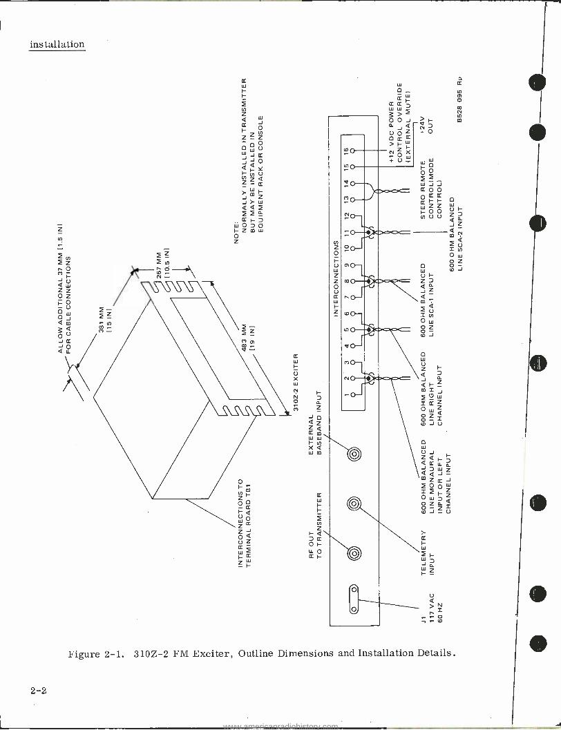
Use only balanced 600 -ohm audio inputs to the 310Z -2. Use only twisted, shielded parts for input cables. (See figure 2-1.)
a. Monaural Inputs - Connect the monaural audio input line to TB1 -1 and TB1 -3. Connect the cable shield to TB1 -2. (See figure 2-1.)
b. Stereophonic Inputs - Connect the left channel audio input line to TB1 -1 and TB1 -3. (See figure 2 -1.) Connect the cable shield to TB1 -2. Connect the right channel audio input line to TB1 -4 and TB1 -6. Connect the cable shield to TB1 -5. Be sure that the 786V -1 Stero Generator is plugged into the 310Z -2.
c. SCA Inputs - Connect the SCA -1 (41 -kHz) audio input to TB1 -7 and TB1 -9. Connect the cable shield to TB1 -8. Connect the SCA -2 (67 -kHz) audio input to TB1 -10 and TB1 -12. Connect the cable shield to TB1 -11. Be sure that the 786W -1 SCA Generator is plugged into the 310Z -2. Set the 786W -1 METER switch to 3. 5 kHz or 7. 5 kHz, depending on the deviation to be used. Set the 786W -1 MUTE ENABLE switch to ON.
d. Composite STL Input - Connect the output of the STL receiver to B/B IN jack J2 on the rear of the exciter. This connection should be made with RG -58A /U or RG -223 coaxial cable. Check to see that the 785E -1 STL card is installed in the A3 card position and that filter FL1 is removed from its socket.
www.americanradiohistory.com
installation
O
` w J J O O ¢ ¢ F. H O Z Z
U Lu
O O Z á J Z Q N Q
2 in O w o Z 0
O w U Z Q Q 2 J Q Q al Z 2O 2 2 O w 0 o - co J
2 H w
H W J J 1 W Z -
U
> n
N 2 O O
Figure 2 -1. 310Z -2 FM Exciter, Outline Dimensions and Installation Details.
2 -2
www.americanradiohistory.com

ins tall ation
e. Radio Remote Control Telemetry Input - Connect the telemetry output of the remote control unit to TELE IN jack J3 on the rear of the exciter. This connection should be made with RG -58A /U or RG -223 coaxial cable. Check to see that a 67 -kHz 786V -1 SCA Generator is installed in the A2 card position.
2.3.2 Stereo Remote Control
If stereo remote control is desired, connect the leads from the station remote control system to TB1 -13 and TB1 -14 (ground). A normally closed contact must be provided for stereo operation.
2.3.3 RF Output
Connect a coaxial cable from the transmitter rf input to the exciter RF OUT jack, J1.
2.3.4 Input Power
Connect the ac line cord between P1 on the exciter and 117 volts ac.
CAUTION
Do not operate the 310Z -2 exciter without a load connected to the rf output, and do not operate the exciter over any extended period of time into a vswr greater than 2:1. To guard against such operation, steps should be taken during installation, as outlined in paragraph 2.3.5.
2.3. 5 Power Control Override
A dc voltage source ( +12 volts) should be connected to TB1 -16 to protect the exciter output transistors when no plate voltage is present in the transmitter. This dc voltage is applied to the power regulator card to reduce the exciter output power to a safe level.
If the override voltage is not available directly from the transmitter with which the exciter is being used, the voltage provided at TB1 -15 of the exciter may be connected through a relay so that it is applied whenever plate voltage is removed from the power amplifier stage in the transmitter.
2.4 INITIAL CHECKS
The 310Z -2 exciter is carefully adjusted and inspected at the factory and no special tests or adjustments are required upon installation. However, once the exciter has been installed, the transmitter should be checked to ensure that it is operating properly.
2. 5 OUTPUT FREQUENCY CHANGE
The output frequency of the 310Z -2 is crystal controlled and can be changed to any desired frequency between 88 and 108 MHz. To change the exciter frequency, refer to paragraph 5. 8.
2-3/2-4
www.americanradiohistory.com


Section 3
Operation
3.1 GENERAL
Only the three front panel switches and the meter on the front panel of the exciter are used during normal operation. Refer to figure 3 -1 for control and indicator locations and to table 3 -1 for control and indicator descriptions. After the exciter has been placed in oper- ation, it is necessary only to check meter indications (table 3 -2) from time to time to ensure that the exciter is operating properly.
3.2 NORMAL TURN -ON PROCEDURE
a. Place POWER switch to ON.
b. Set MODE switch to LEFT, RIGHT, or STEREO, depending on the type of modulation desired.
3.3 ALTERNATE TURN -ON PROCEDURE
When the 310Z-2 is used in a Collins transmitter that has automatic -sequencing circuits, the POWER switch is normally left in the ON position and the exciter is turned on and off by the power- sequencing circuits of the transmitter.
3.4 STEREO /MONAURAL REMOTE SWITCHING
When it is desired to switch the exciter from monaural to stereo from a remote location, a stereo on /off switch is connected between pins 13 and 14 of terminal board TB1. This switch will then control relay Kl so that remote switching can be used as long as the MODE switch is in either the LEFT or RIGHT position. The STEREO position overrides the remote stereo OFF position. The selected LEFT or RIGHT line will then serve as a feed for monaural operation.
www.americanradiohistory.com

operation
M1 S3 S2 R1 F1
ROWER ADJUST
POW .R
F2 S1
Al SC A-1
GENERATOR
A2 SCA -2
GENERATOR
A3 STEREO GENERATOR
A4 MODULATOR
A5 RF AMPLIFIER
Figure 3 -1. 310Z -2 FM Exciter, Front Panel Controls and Indicators.
3 -2
8528 096 Rp
www.americanradiohistory.com

operation
Table 3 -1. 310Z -2 FM Broadcast Exciter, Front Panel Controls and Indicators.
REF DES CONTROL OR INDICATOR FUNCTION
51 POWER Controls the application of primary power to the exciter.
S2 MODE Selects either the left audio input to be broadcast monaurally (LEFT), or the right audio input to be broadcast monau- rally (RIGHT), or the left and right audio inputs to be broadcast stereophonically (STEREO).
S3, M1 METER Meter Ml, in conjunction with function switch S3, permits monitoring of the various audio inputs and dc parameters from the 310Z -2 exciter. Refer to table 3 -2.
R1 POWER ADJUST Adjusts power output of exciter.
Table 3 -2. Test Meter Indications
POSITION OF METER SWITCH S3
FUNCTION METER INDICATION
LEFT Left channel modulation Semi -peak reading meter responds to peak audio level in manner similar to modulation monitor.
RIGHT Right channel modulation Same
B/B Baseband output of stereo generator
Same
SCA -1 41 -kHz sca modulation Calibration at 100% determined by setting of S2 on 786W -1 in Al card position.
SCA -2 67 -kHz sca modulation Same as SCA -1 except card A2
MOD OUT Modulator rf output Relative rf output of modulator. Reads 50% to 100% as noted on individual data sheet.
www.americanradiohistory.com

operation
Table 3 -2. Test Meter Indications (Cont).
POSITION OF METER SWITCH S3
FUNCTION ME TER INDICATION
PA OUT Power amplifier rf Relative rf output of power ampli - output fier. Calibration controlled by R2
on 310Z -2 main frame. Set for 100% under normal power output and load conditions.
24V PS Output of fixed power Reads combined output of fixed 24- supplies of main frame volt power supplies. Normally
reads 85% to 115 %. Reads 40% to 60% when either supply inoperative.
PA Ec Power amplifier Reads relative collector voltage collector voltage to driver and power amplifier
transistors. Consult data sheet for normal readings.
PA le Power amplifier Reads relative collector current collector current to driver and power amplifier
transistors. Consult data sheet for normal readings.
3 -4
www.americanradiohistory.com
Section 4
Theory of Operation
4.1 GENERAL
The 310Z -2 exciter produces a frequency -modulated output for driving a power amplifier in an FM broadcast transmitter. The 310Z-2 employs the direct method of frequency modulation. The optional 786V -1 Stereo Generator produces signals that meet all FCC requirements for stereophonic broadcasting. The optional 786W -1 SCA Generator pro- duces an FM subcarrier for broadcasting background music under an FCC Subsidiary Communications Authorization.
4.2 BLOCK DIAGRAM DISCUSSION
Refer to figure 4 -1 (simplified block diagram), figure 7 -1 (detail block diagram), and figure 7 -2 (main frame schematic) during the following discussion. The major circuits of the 310Z -2 are contained on plug -in modules; and as shown on figure 4 -1, these modules are the major blocks of the 310Z -2 exciter. When an exciter is used for monaural broad- casting without the optional modules, the monaural input is normally applied to the audio - processing circuits and then directly to the modulator module as the baseband signal. Since the remaining circuits operate the same for either monaural or stereophonic and sca broadcasting, the block diagram discussion covers a complete exciter with the optional modules.
The left and right audio input signals are applied through the audio frequency circuits as the modulation input to the balanced modulator of the stereo generator. These signals modulate two 38 -kHz subcarrier signals that are 180° out of phase. As a result, the 38 -kHz carrier is canceled so that the modulator output consists of only the two modulation frequencies and the desired modulation sidebands of the carrier frequency. One component is directly proportional to the sum of the two audio signals (L + R), and the other component is a double - sideband signal (L - R). The output from the balanced modulator is combined with the 19 -kHz pilot carrier. Signal generation within the stereo generator is described in paragraph 4. 3.
The output from the stereo generator is passed through a 53 -kHz low -pass filter and then combined with the output from the sca generator (if used) to produce the baseband signal. The 19 -kHz pilot carrier is derived in the stereo generator by routing one of the 38 -kHz subcarrier signals to a divide -by -2 circuit to produce the 19 -kHz pilot carrier, which is phase -locked to the 38 -kHz signals. The baseband signal is then applied to the modulator.
The sca audio inputs are applied to an audio transformer in the sca generators, routed through a preemphasis network, amplified, and used to frequency -modulate the carrier frequency of the subcarrier. The audio input is also monitored by a carrier mute circuit, which removes the sca output whenever the audio input drops below the selected mute level.
4 -1
www.americanradiohistory.com

theory of operation
4.3 STEREO GENERATOR A2
The 786V -1 Stereo Generator performs the conversion of stereophonic input signals to an output that conforms to the standards approved by the FCC for transmission of stereophonic signals. To provide a realistic stereo effect, the 786V -1 maintains the difference in time delay and signal amplitude from the sound source to both the right and left channel micro- phones through the entire stereo system. Channel separation, which is the isolation be- tween the two channels, is held to greater than 35 dB by the 786V -1 to enhance the stereo effect to the listener. The following paragraphs discuss stereophonic signal generation and the principles of operation of the 786V -1 Stereo Generator. Refer to figure 7 -4 for a schematic diagram of the 786V -1 Stereo Generator.
4. 3. 1 Signals Required
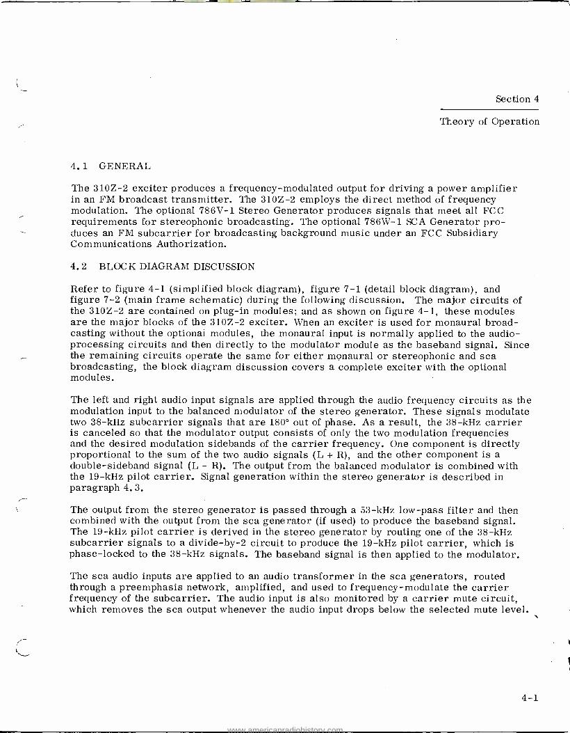
The FCC requires that stereophonic FM broadcast signals be compatible, which means that the signals may be detected by either a monophonic or stereophonic receiver. To satisfy this and other requirements of the FCC, the signals and frequencies generated must be as shown in figure 4 -2. In monophonic receivers only, the L + R (left plus right) audio, frequency component of the signal, called the main channel, is used. The L - R (left minus right) component of the baseband signal, called the subchannel, is a difference signal only and is composed of sidebands of a 38 -kHz suppressed subcarrier. This difference com- ponent and the 19 -kHz pilot carrier signal are reduced by the deemphasis network of the monophonic receiver.
In FM stereophonic receivers, all signals shown in figure 4 -2 are detected and used. The L - R subchannel and L + R main channel signals are mixed, added, and subtracted to separate them into left and right audio signals. The 19 -kHz pilot carrier signal is doubled in the receiver to regenerate the 38 -kHz suppressed subcarrier, which is used to demodulate the stereo signal. By this means, proper phase relationship is maintained between main channel and subchannel frequencies and between the left and right audio channels.
After the L + R and L - R signals have been generated, any interaction or exchange of infor- mation between the main channel (L + R) and the subchannel (L - R) represents crosstalk, which deteriorates the signals and has the effect of adding noise. In stereo transmitting systems, crosstalk must be kept at least 40 dB below either signal - channel level.
To maintain 30 -dB channel separation, as required by the FCC, for the condition of an input into one channel only, the main channel and stereo subchannel signals must have equal peak amplitude, within approximately 0.3 dB, and the envelope of the subchannel signal must cross the zero level simultaneously with the main channel signal, within approximately +30.
4.3.2 Method of Signal Generation in 786V -1 Stereo Generator
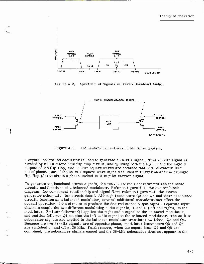
The 786V -1 generates the spectrum of signals shown in figure 4 -2 by the time -division multiplex method. The basic system operating principle is shown in figure 4 -3. The left and right audio channels are switched into the link (used alternately) at a 38 -kHz rate. If the receiver switching rate is synchronized with the transmitter switching rate, the original left and right audio signals are detected. In the receiver the frequency of the 19 -kHz pilot carrier is doubled to synchronize the receiver to the transmitter. It is important that the switching frequency in both the stereo generator and the receiver be of the same phase to retain the identity of the left and right audio signals. In the 786V -1 generator
4 -2
www.americanradiohistory.com
MAIN SUB QIANNEL PILOT CHANNEL
L+R CARRIER L -R
0 50HZ 1
` 19KHZ / i r
15 KHZ 23KHZ
LSB I USB
38 KHZ 53KHZ
theory of operation
B528 087 Rp
Figure 4 -2. Spectrum of Signals in Stereo Baseband Audio.
LEFT CHANNEL
RIGHT CHANNEL
SWITCH SYNCHRONIZATION (38KHZ)
RADIO LINK
7
LEFT CHANNEL
RIGHT CHANNEL
B528 086 Rp
Figure 4 -3. Elementary Time -Division Multiplex System.
a crystal- controlled oscillator is used to generate a 76 -kHz signal. This 76 -kHz signal is divided by 2 in a micrologic flip -flop circuit; and by using both the logic 1 and the logic 0 outputs of the flip -flop, two 38 -kHz square waves are obtained that will be exactly 180° out of phase. One of the 38 -kHz square -wave signals is used to trigger another micrologic flip -flop (A4) to obtain a phase -locked 19 -kHz pilot carrier signal.
To generate the baseband stereo signals, the 786V -1 Stereo Generator utilizes the basic circuits and functions of a balanced modulator. Refer to figure 4 -1, the exciter block diagram, for component relationship and signal flow; refer to figure 7 -4, the stereo generator schematic, for circuit detail. Although transistors Q2 and Q5 and their associated circuits function as a balanced modulator, several additional considerations affect the overall operation of the circuits to produce the desired stereo output signal. Separate input channels couple the two different modulating audio signals, L and R (left and right), to the modulator. Emitter follower Q1 applies the right audio signal to the balanced modulator, and emitter follower Q4 couples the left audio signal to the balanced modulator. The 38 -kHz subcarrier signals are applied to the balanced modulator transistor switches, Q3 and Q6. Because the two 38 -kHz signals are of opposite phase, modulator transistors Q2 and Q5 are switched on and off at 38 kHz. Furthermore, when the ouputs from Q2 and Q5 are combined, the subcarrier signals cancel and the 38 -kHz subcarrier does not appear in the
4 -5
www.americanradiohistory.com

theory of operation
output signal. Transistor Q2 conducts during one half -cycle of the subcarrier frequency, and during this half -cycle one excursion of the square wave is modulated by the audio signal in the right channel. During the next half -cycle of the subcarrier, Q5 conducts and the next excursion of the square wave is modulated by the audio signal in the left channel. As stated previously, the 38 -kHz subcarrier signals are balanced out in the modulator, and only the two modulating audio frequencies and the desired modulation sidebands of the carrier fre- quency are combined in the output.
4.3.3 Analysis of Signals Generated
If can be demonstrated by mathematical analysis that if a square wave is modulated alternately by two audio signals, two significant components are in the resultant signal. One component is directly proportional to the sum of the two audio signals (L + R), and the other component is a double -sideband (DSB) signal centered on the switching frequency or subcarrier frequency (38 kHz). Mathematical analysis in detail is hardly within the scope of this manual. One other fact derived from such analysis is necessary, however, to an understanding of the 786V -1 operation. Because the peak amplitude of the fundamental sine - wave components of a square wave, is 4/7r times the peak amplitude of the square wave itself, the L - R component mentioned above is 4 /7r times the L + R component.
To make L + R = L - R, as required by the FCC, small portions of the L and R signals are added directly in the 786V -1, shunted around the balanced modulator through R9, R25, R16, and C13, and added to the modulator output.
Development of the FCC required signal in the 786V -1 may also be demonstrated by an analysis of the waveforms generated. Figure 4 -4 represents the circuit operation when the inputs to each of the audio channels (L and R) are identical sine waves. On one half -cycle of the square -wave switching frequency (subcarrier frequency), Q5 conducts and the L signal is utilized (or sampled). On the next half -cycle, Q2 conducts and the R signal is utilized. Expressing the same action in a different way, on one half -cycle of the switching frequency an excursion of the subcarrier square wave is modulated by the left channel audio signal; and on the next half -cycle the next excursion of the subcarrier square wave is modulated by the right channel audio signal. As may be seen in figure 4 -4, the 38 -kHz sub - carrier switching frequency is balanced out, and with equal sinewave input to both audio channels (L - R = sine wave) no sidebands are generated. The spikes shown on the composite sine wave in the third illustration of figure 4 -4 are caused by imperfect switching and must be filtered out. The output of the modulator is then a sine wave identical to the original sine -wave input in either channel (L - R or [L + R] /2). Equal sine -wave input seldom occurs in an actual broadcast but is shown here for analysis.
Figure 4 -5 shows the balanced modulator output when L = 1 and R = O. The output of the balanced modulator is an audio component plus DSB components centered on the switching frequency, and odd harmonics. When the odd harmonics are filtered out by a phase -linear low -pass filter, the third waveform results. The audio component is then increased by 4 /,r and the fourth illustration results.
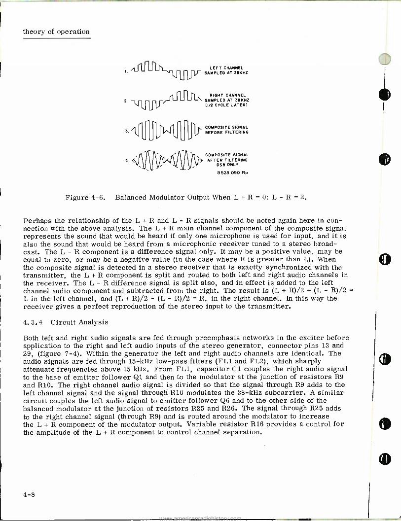
Figure 4 -6 shows the time -division multiplex signal when L = -R, or L + R = 0, and L - R =
2L (or 2R). The composite waveform from the balanced modulator is shown in the third illustration. This waveform is composed of equal but opposite audio components, DSB com- ponents centered on the switching frequency, and odd harmonics. The audio components balance out; and when the odd harmonics are removed by filtering, the waveform in the fourth illustration results. This waveform is a DSB signal, which equals L - R as required.
4 -6
www.americanradiohistory.com

i
LEFT CHANNEL SAMPLED AT 38KHZ
RIGHT CHANNEL SAMPLED AT 38KHZ
COMPOSITE SIGNAL AUDIO OUTPUT
B528 088 Rp
theory of operation
Figure 4 -4. Balanced Modulator Output When L + R = 2; L - R = O.
LEFT AUDIO (RIGHT AUDIO ZERO)
BALANCED MODULATOR OUTPUT WAVEFORM
AFTER FILTERING
AFTER AMPLITUDE CORRECTION
B528 089 Rp
Figure 4 -5. Balanced Modulator Output When L + R = 1; L - R = 1.
4-7
www.americanradiohistory.com
theory of operation
3. N.
W
LEFT CHANNEL SAMPLED AT 38KHZ
RIGHT CHANNEL SAMPLED AT 38KHZ (I/2 CYCLE LATER)
COMPOSITE SIGNAL J BEFORE FILTERING
COMPOSITE SIGNAL AFTER FILTERING
DSB ONLY
B528 090 Rp
Figure 4 -6. Balanced Modulator Output When L + R = 0; L - R = 2.
Perhaps the relationship of the L + R and L - R signals should be noted again here in con- nection with the above analysis. The L + R main channel component of the composite signal represents the sound that would be heard if only one microphone is used for input, and it is also the sound that would be heard from a microphonic receiver tuned to a stereo broad- cast. The L - R component is a difference signal only. It may be a positive value, may be equal to zero, or may be a negative value (in the case where R is greater than L). When the composite signal is detected in a stereo receiver that is exactly synchronized with the transmitter, the L + R component is split and routed to both left and right audio channels in the receiver. The L - R difference signal is split also, and in effect is added to the left channel audio component and subtracted from the right. The result is (L + R) /2 + (L - R) /2 =
L in the left channel, and (L + R) /2 - (L - R) /2 = R, in the right channel. In this way the receiver gives a perfect reproduction of the stereo input to the transmitter.
4.3.4 Circuit Analysis
Both left and right audio signals are fed through preemphasis networks in the exciter before application to the right and left audio inputs of the stereo generator, connector pins 13 and 29, (figure 7 -4). Within the generator the left and right audio channels are identical. The audio signals are fed through 15 -kHz low -pass filters (FL1 and FL2), which sharply attenuate frequencies above 15 kHz. From FL1, capacitor C1 couples the right audio signal to the base of emitter follower Q1 and then to the modulator at the junction of resistors R9 and R10. The right channel audio signal is divided so that the signal through R9 adds to the left channel signal and the signal through R10 modulates the 38 -kHz subcarrier. A similar circuit couples the left audio signal to emitter follower Q6 and to the other side of the balanced modulator at the junction of resistors R25 and R26. The signal through R25 adds to the right channel signal (through R9) and is routed around the modulator to increase the L + R component of the modulator output. Variable resistor R16 provides a control for the amplitude of the L + R component to control channel separation.
4 -8
www.americanradiohistory.com
theory of operation
The 38 -kHz subcarrier signals for the balanced modulator are produced from the output of the 76 -kHz oscillator, transistor Q7 and its associated circuits. The oscillator frequency is controlled by crystal Y1, and after amplification by amplifier Q8 the 76 -kHz signal triggers a flip -flop (micrologic Al). By using both the logic 1 and the logic 0 from this flip -flop, two 38 -kHz signals are obtained that are 180° apart in phase. The output signals from flip - flop Al are first amplified by the inverters (micrologics A2 and A3) and then applied to the modulator through transistor switches Q3 and Q6. Capacitor C26 helps maintain balance between Q3 and Q6 and improves the switching operation. The 38 -kHz signals combine with the right and left channel audio signals at the base of Q2 and Q5 respectively. As a result, Q2 and Q5 alternately conduct at a 38 -kHz rate and produce the stereo signals, which are coupled through C12. The 38 -kHz output from micrologic inverter A3 triggers micrologic flip -flop M. With both the set side (pin 1) and the reset side (pin 3) of the flip -flop grounded, the flip -flop functions as a complementary flip -flop. Thus, the output from the logic 1 side (pin 7) is a 19 -kHz signal that is phase -locked to the 38 -kHz subcarrier signals. The 19- kHz pilot carrier signal is routed through the PILOT CARRIER switch (S1) to a filter network (C29, C23, L2, and C24), which removes the undesired third harmonic of 19 kHz. From the filter the signal is fed through potentiometer R49, which provides control of the pilot carrier amplitude, through capacitor C14 and a resistor network to the output of the balanced modulator.
Bypass capacitors C25 and C4 provide an ac ground for any signal through Q3 when the transistor conducts. Similar capacitors (C27 and C11) perform the same function in relation to Q6. Potentiometers R12 and R28 provide a means for adjusting the sideband suppression. Of special importance in this circuit is suppression of the 76 -kHz harmonics of the 38 -kHz subcarrier. The L - R double -sideband signal from the balanced modulator and the 19- kHz pilot carrier signal are combined, and capacitor C12 couples the combined signal to the multiplex output, connector pin 16. The L + R amplitude correction (from R16 through C13) adds to the signal coupled through C12, to form the composite stereo baseband signal at the multiplex output.
4.4 SCA GENERATOR A1/A2
4.4.1 General
Signals from the 786W -1 SCA Generator become part of the audio baseband signal that is used to modulate the carrier. The subcarrier oscillator is a free - running multivibrator, which generates a 67 -kHz center frequency that is frequency modulated by the sca audio input signal. During normal stereo broadcast operation, modulation is limited to ±3.5 -kHz deviation to avoid interference with the stereo frequencies in the baseband signal. During monophonic broadcasts, ±7. 5 -kHz deviation is used. The modulation output from the oscillator is filtered to remove unwanted harmonics. Refer to figure 4 -1, the exciter simplified block diagram, for component relationship and signal flow; refer to figure 7 -3, sca generator schematic for circuit detail.
4.4.2 Circuit Analysis
The sca audio input is applied to the sca generator through connector pins 17 and 19 (fig- ure 7 -3). The main signal path is through Tl to audio amplifier Q2, but a portion of the input signal is also applied through S2 to the sca audio input of the vu meter, and through the mute level control (potentiometer Rl) to the carrier mute circuits.
4-9
www.americanradiohistory.com

theory of operation
Modulation level control R3 selects the sca audio input level, which is coupled through C 1
to impedance- matching emitter follower Q1. A standard 75- microsecond preemphasis network (consisting of R7, R8, and C3) and capacitor C4 couple the input signal to audio amplifier Q2. Capacitor C30 and switch S2 couple the amplified audio signal to the modulation input of the vu meter. Switch S2 selects the correct attenuation (R46 or R47) of the modulation input signal to provide a 0 -vu indication for either 3.5 -kHz or 7. 5 -kHz frequency deviation. The audio signal used to modulate the subcarrier frequency is applied through CR1 to the subcarrier oscillator circuit. Transistors Q4 through Q7 and their associated circuits comprise the astable multivibrator circuit that generates the 67 -kHz center frequency subcarrier. Deviation of the subcarrier frequency, as adjusted by modulation level R3, is within the range selected ( ±3.5 kHz or ±7. 5 kHz). The modulated rf output from the oscil- lator is coupled through C10 and R3 to the base of amplifier Q8.
The carrier mute circuit is connected to the collector circuit of amplifier Q8 through MUTE ENABLE switch Sl. Whenever the carrier mute circuit is being used (normally) and the audio input level drops below the level selected by MUTE LEVEL control R1, the output from the sca generator is grounded at the collector of Q8. Positive pulses that are normally applied to the base of Q12 are removed, and Q12 is turned off. As a result, C27 charges through R43 toward +20 volts; and when a potential of +10 volts is reached (in 3 seconds), diode CR9 breaks down and a positive voltage is applied to the base of Q13. Consequently, the collector of Q13 is at ground potential and this ground is applied through S1 to the collector of Q8.
Assuming that the input level is greater than the threshold level selected by MUTE LEVEL control R1, the modulated signal from the subcarrier oscillator is amplified by the direct - coupled amplifier (Q8 and Q9) and applied through CR7, R32, and R51 to the filter network. Capacitors C12 through C21 and inductors Ll through L3 comprise a 2- section band - shaping filter that removes the unwanted harmonics of the 67 -kHz subcarrier. Capacitor C22 couples the filtered signal to emitter follower Q10, which provides a low output im- pedance to feed the SCA subcarrier signal through capacitor C23 and connector pin 43 to the input of the FM modulator card of the exciter.
4.5 FM MODULATOR A4
The FM modulator is a direct FM modulator operating at carrier frequency. A phase -lock automatic frequency control system controls the output frequency within very tight tolerances. Refer to figure 7 -5, modulator schematic, for circuit details.
Transistor Q1 is operated class A as a Clapp oscillator with inductor L5 as the oscillator tank coil. The frequency of oscillation is determined by L5 and the net capacitive reactance formed by CR3, CR4, CR5, CR6, C4, C15, C7, C8 and C9. Elements CR3, CR4, CR5 and CR6 are voltage -variable capacitors, or varicaps, whose terminal capacitance is an inverse function of applied voltage. Varicaps CR3 and CR4 are operated with a fixed dc bias as modulators. The bias is adjustable by R5 and is set for best linearity in final test. Varicaps CR5 and CR6 are operated with two independent bias voltages chosen in a manner such that the devices cannot be forward biased. The more positive of the two volt- ages is controlled by AFC ADJUST control R7 and is used as a fine frequency or phase adjustment for the modulator. The lower of the two voltages is derived from the phase detector loop filter or from a fixed dc voltage for test purposes.
4 -10
www.americanradiohistory.com

theory of operation
The modulator circuits are temperature compensated by capacitors C7, C8 and C9 to reduce drift. Isolation from the load is enhanced by a T -pad consisting of resistors R18, R19, and R20. Buffer stage Q2 is operated at approximately 500 milliwatts. The collector circuit is coupled to the load through a Pi network consisting of L8, C24, and C25. A resistive pad consisting of R26, R27, and R28 further isolates load variations from the modulator circuits. An rf sample is derived from the buffer through C22, clipped by diodes CR10 and CR11, and then coupled to U1, a high -speed ECL (emitter -coupled logic) binary divider. The output of the divider is amplified and shaped in an amplifier composed of Q3, Q4 and associated circuits and applied to complementary -MOS divider U2. Divider U1 divides the carrier frequency input by a factor of 16 while divider U2 divides its input by 1024 for a total division of 16, 384.
The reference crystal is enclosed in an oven at 75° centigrade and operates at 1/64 of carrier frequency. The reference oscillator is an untuned device consisting of integrated circuit U5 and associated components. A vernier frequency adjustment is included in the form of a screwdriver adjustment, C38, accessible from the front panel. The capacitor provides sufficient adjustment range to compensate for aging of the crystal.
The output of the oscillator is divided by a factor of 128 in divider U4 and further divided by a factor of 2 in one -half of divider U3. The other half of U3 is a simple flip -flop that acts as a phase detector. The device is clocked by the divided reference frequency signal at a rate 1/256th of the crystal frequency. The flip -flop is then reset by a narrow pulse derived from the divided modulator output signal. The large division ratio of the modulator divider effectively removes the phase shift associated with the frequency modulation process. The resultant phase deviation at the output of the divider is a very small fraction of the available phase detector range at the lowest modulating frequency of interest.
The output of phase detector U3B is a rectangular phase with a duty cycle that is a function of the time difference of the input clock and reset pulses; hence, a function of the phase angle between the modulator and reference oscillator zero crossings. This pulse is amplified by transistor Q7 and filtered by a network consisting of R53, R54, C33, and C34 to reject the comparison frequency and retain the dc component of the pulse. This dc voltage is displayed on meter M1 as an aid in initial setup and maintenance. A green band is shown on the meter as a recommended operating range, and the meter is set by the AFC ADJUST control R7, a front panel adjustment.
The dynamic characteristics of the loop are established by a loop filter consisting of R15, R16, C10, and C ll. The time constants are chosen for best compromise between minimum .
lock acquisition time and minimum disturbance of low- frequency phase response of the modulator system.
If phase -lock is lost, the input frequencies to the phase detector will be unequal and a beat note will appear at the output of the detector. This beat note is ac coupled from amplifier Q8 to a 3. 5 -kHz low -pass filter and further amplified by amplifier Q9. A series of constant - amplitude pulses with a repetition rate proportional to the difference frequency appear at Q9 collector. These pulses are rectified and used to turn on transistor Q5, which activates ALARM lamp CR16 and turns off transistor switch Q6. Switch Q6 applies a dc bias to the power amplifier regulator, which squelches the exciter rf output, thus preventing off - frequency operation. A charging current is applied to the AFC loop filter causing capacitor C10 to charge to a value much greater than its normal value. Four -layer diode CR18 conducts when this charge reaches a certain value and discharges C10 to a value much lower
4 -11
www.americanradiohistory.com
theory of operation
than its normal value. The charging current then slowly recharges C10 and sweeps the oscil- lator frequency through its normal operating frequency. When the correct frequency is reached, the loop is locked and the charging current is removed. At this time ALARM lamp CR16 is extinguished and the dc bias is removed from the pa power supply allowing normal operation to resume. This circuit allows much faster lock acquisition and more optimum loop time constants for the application to be employed.
Transistors Q10, Q11 and associated components are used to provide a "soft" turn -on and turnoff for the crystal oven heater to minimize transients in the modulator. The cir- cuit is straight forward with Q10 operating as a current amplifier and Q11 operating as a saturated switch.
4.6 AUDIO /REGULATOR CARD A7
Audio preemphasis for both monaural and stereo operating modes is obtained from feedback shaping in a pair of high -gain, integrated circuit, operational amplifiers. Both channels are fed from balanced 600 -ohm lines through H pads and transfomers to eliminate effects of uneven source impedances. The left channel response is determined by components R57, R58, R59, R60, C20, C21, and C22. All are fixed low tolerance components. Right channel response is determined by similar components with the addition of three vernier elements R41, R45, and R42, which allow trimming overall gain, mid -frequency and high - frequency gain, respectively to permit matching of response of both channels to a very high degree. This is done to minimize linear crosstalk in the stereo mode, which results from uneven gain and phase tracking of the left and right channels.
Variable resistor R30 provides a vernier setting of monaural gain to permit matching that mode to stereo operation.
Relay K1 is included to permit selection of stereo or monaural operation either locally or by remote control.
4.7 785E -1 STL INTERFACE CARD A3
The 785E -1 STL Interface Card provides an interface between commonly used composite STL systems or other operating modes such as quadraphonic operation requiring an external baseband input to the modulator. The 785E -1 provides input processing and the necessary gain and phase linearity to accommodate these systems. Refer to figure 7 -7. A bridging input of approximately 4700 ohms is provided in a differential input configuration to avoid any degradation of signal -to -noise ratio through ground loops. An adjustable common mode rejection control, R4, is provided to minimize hum. A high frequency phase adjustment, C7, is provided to compensate for minor phase degradation at high frequencies due to receiver and transmitter bandwidth limitation.
Integrated circuit U1 is a low -noise wideband operational amplifier connected as a balanced differential input amplifier. A complementary symmetry power booster stage composed of transistors Q1 and Q2 raises the load impedance to a value suitable for U1. An output pad consisting of R16 and R17 reduces the output level of the amplifier to approximately 200 mV required by the modulator. Capacitor C7 provides a minor phase adjustment at the high end of the spectrum to compensate for phase errors in the system.
4 -12
www.americanradiohistory.com

theory of operation
4,8 RF AMPLIFIER A5
The rf amplifier card of the 310Z -2 contains a broadband, solid- state, 3 -stage rf amplifier. The FM signal from the rf mixer is amplified to provide an rf output power level of 10 to 20 watts. Refer to figure 7 -6 for circuit details.
The first amplifier stage (Q1, figure 7 -6) receives the FM input signal (through jack J1) and operates as a class A amplifier, using 20 -volt dc power supplied through filter FL1. The second and third stages (Q2 and Q3) operate as class C amplifiers so that greater efficiency is obtained. All three amplifier stages are set for gain saturation, which is permissible with an FM input signal and provides higher efficiency. Both Q2 and Q3 use a variable 10- to 26 -volt dc power input through FL2. The rf output power level of the am- plifier (adjustable from 10 to 20 watts) is controlled by the level of this variable dc power, which is adjustable by the POWER ADJUST control mounted on the front panel. The rf amplifier output is coupled through J2 to J1 on the exciter main chassis.
4,9 POWER SUPPLIES
Three power supplies are used in the 310Z -2 exciter. Two are fixed, regulated supplies capable of supplying 24 volts at approximately 700 mA each. One is a variable supply for the rf amplifier. The variable supply supplies up to 26 volts at approximately 2 amperes. All three power supplies are derived from a common, power transformer, rectifier, and filter system. Separate regulators are utilized for each function.
Regulators U1 and U2 are each fixed 24 -volt 3- terminal regulators, which supply the basic exciter requirements. Regulator U1 supplies power to the audio and meter amplifier circuits, Al card, and A4 card. Regulator U2 supplies power to the A2 card, A3 card, and the fixed voltage requirements of the A5 card.
Power for the driver and rf amplifier stages is supplied by an adjustable regulated power supply. This supply consists of an integrated circuit regulator (U2 on the A6 card) and associated components. The regulator supplies base bias voltage for current amplifier transistor Q1, which in turn supplies series pass transistor Q2. The power supply incorporates foldback current limiting to prevent damage to components in the event of short circuits. Overvoltage protection is provided by scr Q7 on the A6 card. Zener diode VR1 sets the point at which the scr fires. This circuit prevents possible damage to the power amplifier transistors in the event of failure of the regulator circuit. When the threshold is exceeded, the scr fires placing a short circuit across the pa power supply. If there is a failure of regulator transistor Q2, then fuse F2 will blow. If the trouble is of a transient nature only, the scr will fire and cause the power supply to go into the current -limiting mode. In this case, simply turning the power supply off and then on will restore proper operation.
Two external control inputs are provided for remote power control and muting purposes. Transistor Q10 on the A6 card serves as an inverter amplifier. The alarm circuit of the modulator supplies a fixed output voltage under alarm conditions, which is coupled to the base of transistor Q10 causing it to saturate and remove the base driver to the power transistors, thus muting the rf output of the exciter.
External mute input, TB1 -16, is provided for external power control or muting purposes. It is coupled to the inverting input of regulator U2 on the A6 card. Full or partial muting of the power output is possible by adjustment of the applied voltage.
4 -13
www.americanradiohistory.com

theory of operation
4.10 METER AMPLIFIER
The peak voltmeter circuit is contained on audio /regulator card A7 and is used to monitor the following audio levels in the 310Z -2:
Left audio level
Right audio level
Stereo generator baseband output
SCA -1 modulation
SCA -2 modulation
The peak voltmeter circuit is an automatic slideback peak voltmeter type that determines the peak voltage of the complex waveforms monitored by the meter. A basic slideback voltmeter operates by reverse -biasing a diode to a point where the incoming signal can no longer switch on the diode. The reverse dc bias voltage is then equal to the incoming peak voltage (disregarding the intrinsic standoff voltage of the diode). The automatic slideback voltmeter operates in a similar manner by taking the signal voltage that is conducted through the reverse -biased diode, amplifying the signal, rectifying it, and applying the resultant dc as a reverse bias to the diode. The diode will conduct until the dc reverse bias from the amplifiers cuts off diode conduction.
Grounded emitter amplifier Q1 amplifies the wideband complex waveform and feeds it to emitter follower amplifier Q2. The resultant signal is applied to peak detector Q2. At the instant that the first half -cycle of the input complex waveform appears on the base of Q2, the transistor conducts, causing the base signal to appear across load resistor R14. Capacitor C7 couples the signal to peak amplifier Q4. The signal output from Q4 is fed to rectifier Q5, which rectifies the signal and charges capacitor C 10 in the negative direction. Capacitor C10 averages the negative output from Q5 into a negative dc potential that appears at the base of feedback bias amplifier Q6. With this negative bias present at the base of PNP transistor Q6 the transistor conducts, increasing the voltage drop across resistor R21. This drives the emitter of Q2 in the negative direction, biasing the transistor to the point where only a small signal peak is conducted by Q2. This reduces the signal voltage across load resistor R14 when the succeeding half- cycles of the wideband input waveform arrive at the base of the peak detector transistor. Due to the gain of transistor stages Q2 and Q4, any conduction of transistor Q2 causes the voltage at the base of Q6 to be sustained at a level that permits Q2 to conduct only during a small portion of the signal peaks. The voltage at the collector of Q2 is then proportional to the peak voltage of the complex wideband waveform. In positions 1 through 5, meter switch S3 connects this voltage through dropping resistor R23 to the front panel meter.
4 -14
www.americanradiohistory.com

Section 5
Maintenance
5.1 GENERAL
The 310Z -2 FM Broadcast Exciter, which contains all solid -state circuits, has been care- fully inspected and adjusted at the factory by skilled technicians using special test equip- ment. Therefore, the 310Z -2 should not be readjusted as part of routine maintenance procedures, but instead should be readjusted only after trouble has definitely been traced to misadjustment. When the 310Z -2 is readjusted, adjustments should be performed in accordance with the procedures outlined in paragraph 5.6 using the recommended test equipment listed in table 5 -1.
To ensure peak performance and maximum service life, a regular schedule of routine maintenance should be carried out. For the 310Z -2 this routine maintenance should consist only of cleaning and inspecting, and should occasionally include a check of the minimum performance standards for the 310Z -2 in accordance with paragraph 5.7.
CAUTION
The 310Z -2 exciter should not be operated without a load connected to the rf output, and should not be operated over any extended period of time into vswr greater than 2 :1.
5.2 CLEANING
Clean the 310Z -2 whenever a perceptible quantity of dust accumulates at any point inside the equipment. A solvent consisting of the following mixture may be used as a cleaning material.
Methylene chloride, 25 percent
Perchlorethylene, 5 percent
Drycleaning solvent, 70 percent by volume
Use the following procedure:
a. Remove dust from chassis, panels, and components with a soft -bristled brush.
b. Clean flat surfaces and accessible areas with a lintless cloth moistened with solvent, removing any foreign matter adhering to the equipment. Dry with a clean, dry, lintless cloth.
c. Wash switch contacts and the less accessible areas with solvent lightly applied with a small soft -bristled brush.
5 -1
www.americanradiohistory.com

maintenance
Table 5 -1. Required Test Equipment.
ITEM MANUFACTURERS DESIGNATION
Wideband FM modulation monitor Collins 900C -3, part no. 758 -5812 -001
Distortion and noise meter Hewlett- Packard 334A
Audio vtvm Hewlett- Packard 400L
Vtvm Hewlett- Packard 410B
Wattmeter Sierra 164B with 181A/250 plug -in element
Stereo test circuit Fabricated per figure 5 -3
Low -distortion of signal generator Hewlett- Packard 306A
Oscilloscope Tektronix 581A
Vertical amplifier Tektronix type 81
Crosstalk test circuit Fabricated per figure 5 -6
FM frequency monitor Collins 54N -1
SCA monitor Collins 900F -1
d. Use a burnishing tool on relay contacts if contacts are corroded or pitted. Apply solvent lightly to relay contacts with a small soft -bristled brush. Dry with a clean, dry, soft -bristled brush.
e. Use a dry, oil -free jet of air to remove any dust accumulated on the modules, circuit cards, in the card cage, or on components located in the area above the cage.
5.3 LUBRICATION
No lubrication is required.
5.4 INSPECTION
Perform periodic visual inspection of the 310Z-2 at least once each month. Inspect all metal parts for rust, corrosion, and general deterioration. Check circuit cards, wiring, and components for signs of overheating. Check the blower and cabinet fan for normal operation. Check all operating controls for smoothness of operation. Check all connections.
5.5 TEST EQUIPMENT REQUIRED
The test equipment listed in table 5 -1, or its equivalent, is required to perform the adjust- ment and test procedures given in this section.
5 -2
www.americanradiohistory.com
maintenance
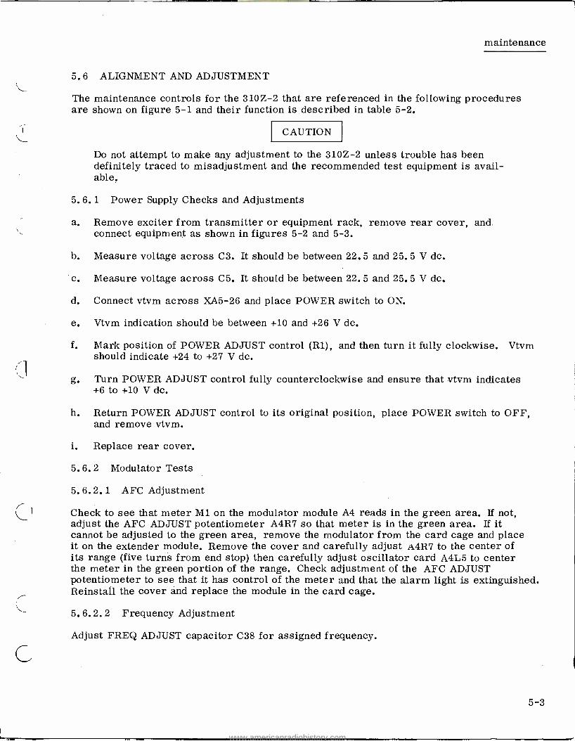
5.6 ALIGNMENT AND ADJUSTMENT
The maintenance controls for the 310Z -2 that are referenced in the following procedures are shown on figure 5 -1 and their function is described in table 5 -2.
CAUTION
Do not attempt to make any adjustment to the 310Z -2 unless trouble has been definitely traced to misadjustment and the recommended test equipment is avail- able.
5.6.1 Power Supply Checks and Adjustments
a. Remove exciter from transmitter or equipment rack, remove rear cover, and . connect equipment as shown in figures 5 -2 and 5 -3.
b. Measure voltage across C3. It should be between 22.5 and 25.5 V dc.
c. Measure voltage across C5. It should be between 22.5 and 25.5 V dc.
d. Connect vtvm across XA5 -26 and place POWER switch to ON.
e. Vtvm indication should be between +10 and +26 V dc.
f. Mark position of POWER ADJUST control (R1), and then turn it fully clockwise. Vtvm should indicate +24 to +27 V dc.
g. Turn POWER ADJUST control fully counterclockwise and ensure that vtvm indicates +6 to +10 V dc.
h. Return POWER ADJUST control to its original position, place POWER switch to OFF, and remove vtvm.
i. Replace rear cover.
5.6.2 Modulator Tests
5.6.2.1 AFC Adjustment
Check to see that meter M1 on the modulator module A4 reads in the green area. If not, adjust the AFC ADJUST potentiometer A4R7 so that meter is in the green area. If it cannot be adjusted to the green area, remove the modulator from the card cage and place it on the extender module. Remove the cover and carefully adjust A4R7 to the center of its range (five turns from end stop) then carefully adjust oscillator card A4L5 to center the meter in the green portion of the range. Check adjustment of the AFC ADJUST potentiometer to see that it has control of the meter and that the alarm light is extinguished. Reinstall the cover and replace the module in the card cage.
5.6.2.2 Frequency Adjustment
Adjust FREQ ADJUST capacitor C38 for assigned frequency.
5 -3
www.americanradiohistory.com

maintenance
A1R3 A2S2 A2R3 A3S1 A3R12 A3R16 A4R5 A4R7 A4S1
A2S1 A2R30 A3R28 A3R49
A7R45
A4CR16
A7R30
A4C38
A7R41 A7R42 A7R10
J1 J4 J3 J2
A4R1
A4M1
TB1 B528 097 Rp
Figure 5 -1. 310Z-2 FM Exciter, Maintenance Controls.
5 -4
www.americanradiohistory.com

maintenance
Table 5 -2. Maintenance Controls.
CONTRO L FUNC TION
786W -1 SCA Generator Card Al /A2
R3 - modulation level
R1 - mute level
R30 - output level
R19 - frequency
S1 - mute enable
S2 - 7. 5 -KHZ DEV /3.5 -KHZ DEV sca deviation switch
786V -1 Stereo Generator Card A3
R12 - sideband suppression
R28 - sideband suppression
R16 - channel separation
R49 - pilot carrier level
S1 - pilot on /off switch
Modulator Card A4
Rl - B/B LEVEL
R7 - AFC ADJUST
Sets the sca audio input levels to the sca modulator.
Sets the minimum audio level that will activate the sca subcarrier mute circuit.
Sets the sca subcarrier output level.
Sets the sca subcarrier frequency.
ON position enables mute circuit to remote the 67 -kHz sca oscillator output when there is no sca audio input. OFF position disables mute circuit for maintenance.
7.5 -KHZ position causes the front panel meter to indicate 0 vu when S3 is in the corresponding SCA -( ) position and sca subcarrier deviation is 7.5 kHz.
3.5 -KHZ position causes the front panel meter to indicate 0 vu when S3 is in the corresponding SCA -( ) position and sca subcarrier deviation is 3. 5 kHz.
Sets the switching point of Q3.
Sets the switching point of Q6.
Sets the level of the L + R signal from Q1 and Q4 applied to the multiple output to give proper levels for good stereo channel separation.
Sets the level of the 19 -kHz pilot carrier applied to the multiplex output.
Switches the 19 -kHz pilot carrier to the multiplex output.
Adjusts baseband modulation sensitivity .
Adjusts free - running frequency of modulator.
5 -5
www.americanradiohistory.com

maintenance
Table 5 -2. Maintenance Controls (Cont).
CONTROL FUNCTION
C38 - FREQ adjust Sets exciter center frequency.
S1 - AFC ON /OFF Disables AFC system for test purposes.
R5 - mod bias Sets bias voltage on modulator diodes for best linearity.
L5 - oscillator frequency Sets coarse frequency modulator.
CR16 - ALARM Provides out -of -lock indication for AFC circuit.
M1 - AFC LEVEL meter Displays AFC voltage.
Audio /Meter Regulator Card A7
R30 - monaural gain vernier Matches monaural mode to stereo operation
R10 - meter amplifier adjust Adjusts meter deflections by 10 percent
R41 - overall gain vernier Allows matching of both stereo channels
R45 - mid -frequency gain vernier Same.
R42 - high- frequency gain vernier Same.
AUDIO SIGNAL GENERATOR (HP -206A)
STEREO TEST
CIRCUIT
}LEFT
310Z -2FM EXCITER
4
6 RIGHT
RF OUTPUT
RF WATTMETER
FM SCA
MODULATION MONITOR MONITOR (900F -1) (900C -3)
DUMMY FM
LOAD TRANSMITTER
FM FREQUENCY
MONITOR (54N -I)
B528 093 Rp
Figure 5 -2. Test Equipment Connections to 310Z -2 for Adjustment and Test Procedures.
5 -6
www.americanradiohistory.com
maintenance
AUDIO INPUT
O \ . MCI
NOTE: TRANSFORMER IS UTC TYPE A43
}
RIGHT AUDIO
OUTPUT
LEFT AUDIO
OUTPUT
B528 091 Rp
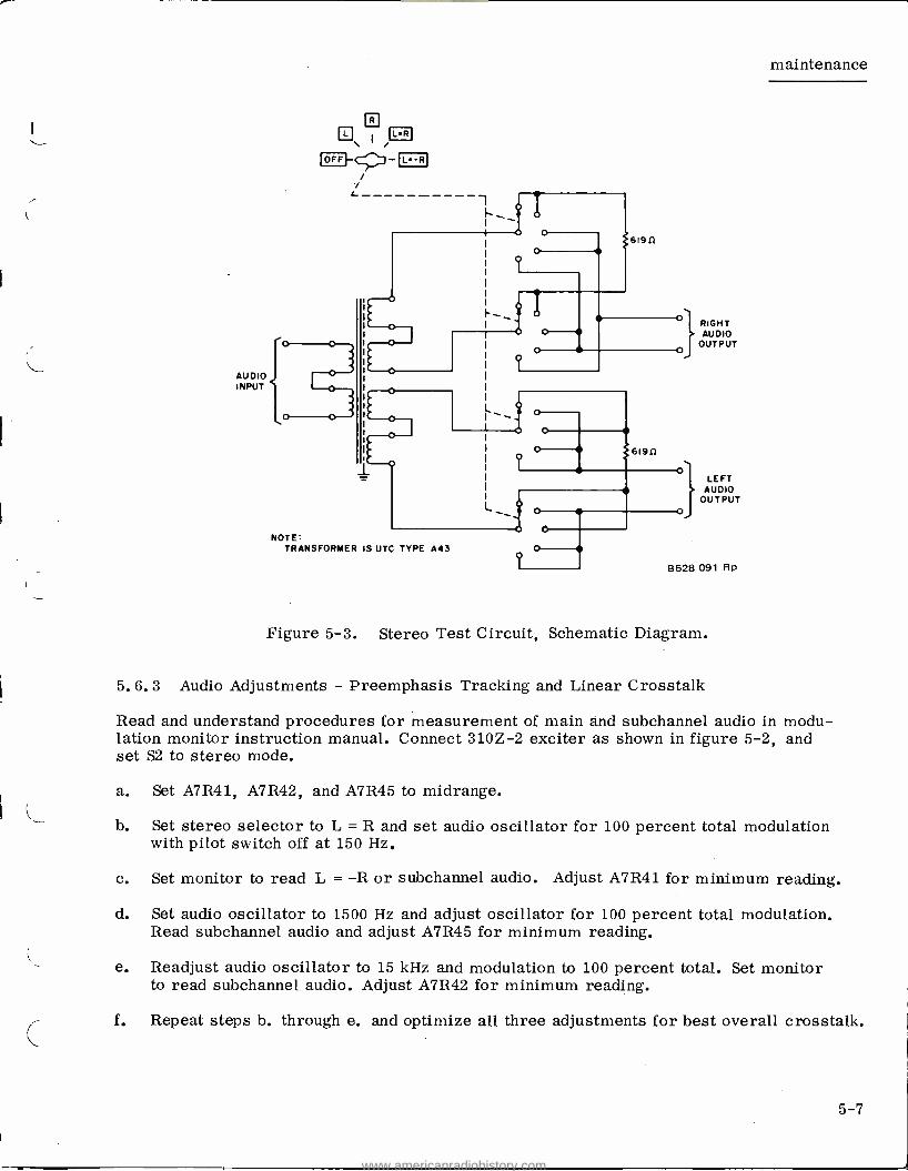
Figure 5 -3. Stereo Test Circuit, Schematic Diagram.
5.6.3 Audio Adjustments - Preemphasis Tracking and Linear Crosstalk
Read and understand procedures for measurement of main and subchannel audio in modu- lation monitor instruction manual. Connect 310Z -2 exciter as shown in figure 5 -2, and set S2 to stereo mode.
a. Set A7R41, A7R42, and A7R45 to midrange.
b. Set stereo selector to L = R and set audio oscillator for 100 percent total modulation with pilot switch off at 150 Hz.
c. Set monitor to read L = -R or subchannel audio. Adjust A7R41 for minimum reading.
d. Set audio oscillator to 1500 Hz and adjust oscillator for 100 percent total modulation. Read subchannel audio and adjust A7R45 for minimum reading.
e. Readjust audio oscillator to 15 kHz and modulation to 100 percent total. Set monitor to read subchannel audio. Adjust A7R42 for minimum reading.
f. Repeat steps b. through e. and optimize all three adjustments for best overall crosstalk.
5 -7
www.americanradiohistory.com

maintenance
g. Repeat steps b. through e. without readjustment of A7R41, A7R42, and A7R45 feeding L = -R and reading main channel audio.
h. Make minor readjustments to A7R41, A7R42, and A7R45 if necessary for best overall crosstalk measurements from subchannel to main channel and main channel to sub - channel. They should exceed 45 dB for all frequencies from 50 Hz to 15 kHz.
i. Set up exciter in STEREO mode and feed +10 dB mW at 400 Hz into the left channel. Turn on the 19 -kHz pilot and adjust it to 9 percent. Read total modulation on the modulation monitor. Adjust B/B LEVEL control A4R1 on the modulator for 100 percent.
j. Set exciter to left mono mode and adjust A7R30 for 100 -percent modulation.
5.6.4 SCA Generator Output Level Adjustment
a. With equipment connected as shown in figure 5 -2, set MODULATOR METER switch on FM modulation monitor to SCA MOD.
b. Place MUTE ENABLE switch (on sca generator card) to OFF.
c. Adjust OUTPUT LEVEL control R30 for 10- percent modulation as indicated on the 0- to 30- percent scale on FM modulator monitor.
d. Turn MUTE ENABLE switch to ON and note that indication on the FM modulation monitor decreases to zero.
5.6.5 SCA Generator Frequency Adjustment
a. With equipment connected as shown in figure 5 -2, turn stereo test circuit switch to OFF.
b. Check the sca output frequency as indicated on the sca frequency monitor (Collins 900F -1 or equivalent).
c. Adjust A1R19 until sca frequency monitor indicates 67 kHz.
5.6.6 Stereo Generator Adjustment
a. Connect equipment as shown in figure 5 -2.
b. Set MODE switch on 310Z -2 front panel to STEREO.
c. Set MODULATION METER switch on FM modulator monitor to TOTAL MOD.
d. Place 19 -kHz pilot carrier switch on stereo generator card to ON.
e. Turn stereo test circuit (figure 5 -3) switch to L position (left modulation only).
f. Set audio oscillator (HP206A or equivalent) to 5000 Hz and adjust the output amplitude for 100 -percent total modulation on FM modulation monitor.
g.
5 -8
Read separation on monitor and adjust R16 on the stereo generator for best separation.
www.americanradiohistory.com

maintenance
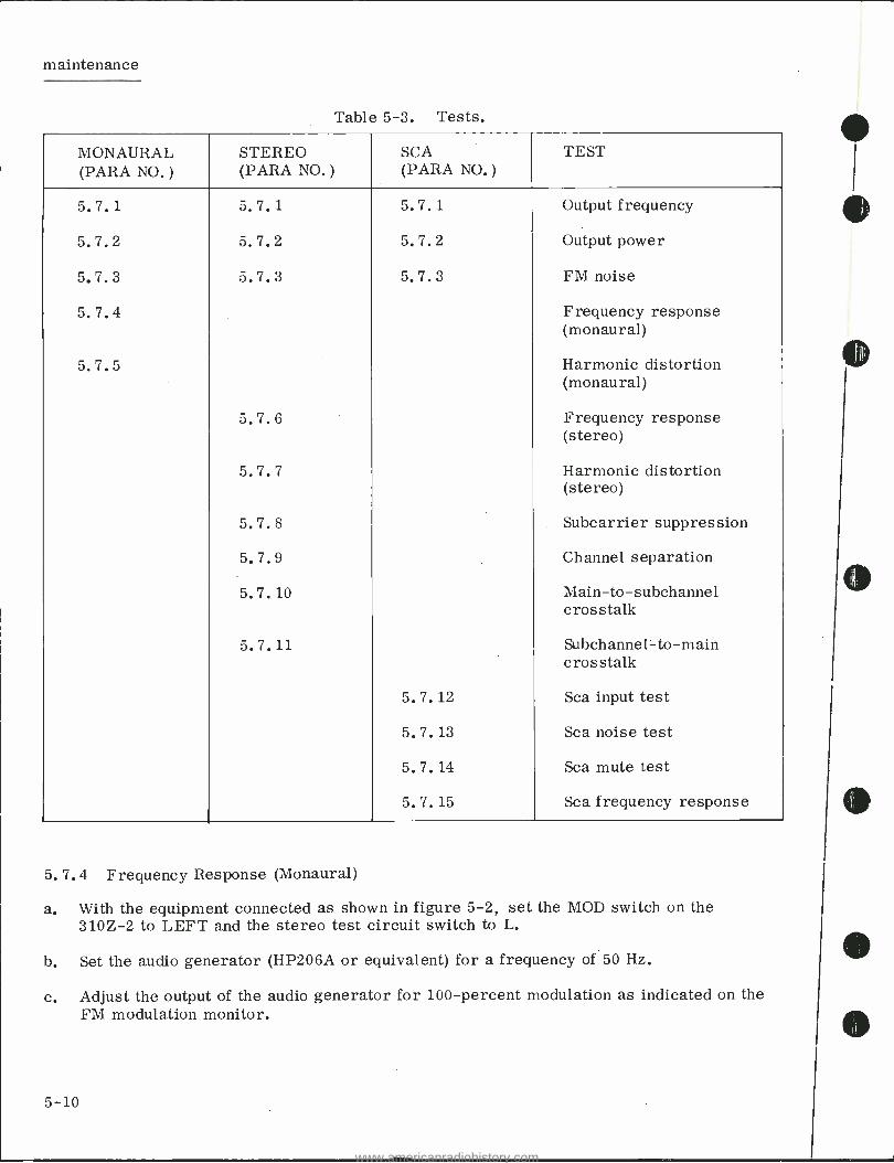
5.7 MINIMUM PERFORMANCE STANDARDS
The 310Z-2 should be tested in accordance with the following procedures after alignment and adjustment. In addition, the following tests should be used to determine if the 310Z -2 is operating properly. Table 5 -3 lists those tests that are applicable to monaural, stereo, and SCA functions of the 310Z -2. If it is desired to test the 310Z -2 for monaural only, perform only those tests listed in table 5 -3 for monaural, etc.
5.7.1 Output Frequency
a. Connect the equipment as shown in figure 5 -2, and turn stereo test circuit switch to OFF.
b. Place POWER switch to ON and measure output frequency. Allow 10 minutes warmup.
c. If the output frequency is incorrect (should be the customer -selected frequency of 88 to 108 MHz), readjust the frequency control on the FM modulator.
5.7.2 Output Power
a. Connect equipment as shown in figure 5 -2.
b. Adjust OUTPUT POWER control until rf wattmeter indicates desired power output.
5.7.3 FM Noise
a. Connect the equipment as shown in figure 5 -2.
b. Turn MODE switch on 310Z -2 to LEFT.
c. Turn MODULATION METER switch on the FM modulation monitor to TOTAL MOD.
d. Turn stereo test circuit switch to L.
e. Set output of audio oscillator to 400 Hz and 100 -percent modulation as indicated on the FM modulation monitor.
f. Turn DECIBELS switch on FM modulation monitor to 0 and METER switch to MAIN CHAN AUDIO.
g. Turn METER ADJUST control until 0 dB is indicated on FM modulation monitor front panel meter.
h. Remove 400 -Hz monaural input signal and turn the DECIBELS switch clockwise until a reading is observed on the meter.
i. The main channel FM noise is the algebraic sum of the DECIBELS switch and the meter indication, and should be no more than -65 dB.
j. Turn METER switch to SUB CHAN AUDIO.
k. The subchannel FM noise is the algebraic sum of the DECIBELS switch setting and the meter indication, and it should be no more than -65 dB.
5-9
www.americanradiohistory.com
maintenance
Table 5 -3. Tests.
MONAURAL (PARA NO. )
STEREO (PARA NO.)
SCA (PARA NO.)
TEST
5.7.1 5.7.1 5.7.1 Output frequency
5.7.2 5.7.2 5.7.2 Output power
5.7.3 5.7.3 5.7.3 FM noise
5. 7.4 Frequency response (monaural)
5.7.5 Harmonic distortion (monaural)
5. 7. i5 Frequency response (stereo)
5. 7. 7 Harmonic distortion (stereo)
5.7.8 Subcarrier suppression
5.7.9 Channel separation
5.7. 10 Main -to- subchannel crosstalk
5.7.11 Subchannel -to -main crosstalk
5.7. 12 Sca input test
5.7. 13 Sca noise test
5.7. 14 Sca mute test
5. 7. 15 Sca frequency response
5. 7.4 Frequency Response (Monaural)
a. With the equipment connected as shown in figure 5 -2, set the MOD switch on the 310Z -2 to LEFT and the stereo test circuit switch to L.
b. Set the audio generator (HP206A or equivalent) for a frequency of 50 Hz.
c. Adjust the output of the audio generator for 100- percent modulation as indicated on the FM modulation monitor.
5 -10
www.americanradiohistory.com

maintenance
d. Vary the audio generator and maintain 100 -percent modulation for frequencies of 100, 400, 1000, 5000, 7500, 10, 000 and 15, 000 Hz.
e. Ensure that attenuator settings for each frequency are within the limits of the 75- microsecond preemphasis curve as defined by the FCC.
5. 7. 5 Harmonic Distortion (Monaural)
a. Connect the equipment as shown in figure 5 -2.
b. Turn MODE switch on the 310Z -2 to the LEFT position.
c. Turn MODULATION METER switch on the FM modulation monitor (900C -3) to TOTAL MOD and the DE- EMPHASIS switch to IN.
d. Turn stereo test circuit switch to L.
e. Set the audio oscillator (HP206A) to 50 Hz, and adjust the output amplitude for 100 - percent total modulation on the FM modulation monitor.
f. Turn MODULATION METER switch on FM modulation monitor to MAIN CHAN AUDIO.
g. Connect distortion meter (HP334A or equivalent) to the DISTORTION METER jack on the FM modulation monitor.
h. Ensure that the distortion meter indication is not more than 0.25 percent.
i. Repeat steps e. through h. for modulating frequencies of 100, 400, 1000, 5000, 7500, 10, 000 and 15, 000 Hz.
5.7.6 Frequency Response (Stereo)
a. With equipment connected as shown in figure 5 -2, set the MODULATION switch on the 310Z -2 to STEREO and the stereo test circuit switch to LEFT.
b. Turn on 19 -kHz pilot.
c. Repeat steps b. through e. of paragraph 5.7.4.
d. Place STEREO TEST CIRCUIT switch to RIGHT.
e. Repeat steps b. through e. of paragraph 5.7.4.
5.7.7 Harmonic Distortion (Stereo)
a. With equipment connected as shown in figure 5 -2, place PILOT CARRIER switch to ON.
b. Turn MODE switch on 310Z -2 to STEREO.
c. Turn MODULATION METER switch on 900C -3 to TOTAL MOD, and place DE- EMPHASIS switch to OUT,
5 -11
www.americanradiohistory.com

maintenance
d. Set switch on stereo test circuit (figure 5 -3) to L = R.
e. Set audio oscillator (HP206A) to 50 Hz, and adjust output amplitude for 100- percent total modulation on 900C -3.
f. Connect distortion meter (HP334A or equivalent) to LEFT AUDIO jack on the 900C -3.
g. Measure and record total distortion for modulating frequencies of 50, 100, 400, 1000, 5000 and 7500 Hz. Maintain modulation on 900C -3 at 100 percent for all fre- quencies, and distortion should be not more than 0.5 percent.
h. Connect distortion meter to RIGHT AUDIO jack on 900C -3 and repeat step g.
5.7.8 Subcarrier Suppression
a. With equipment connected as shown in figure 5 -2, place PILOT CARRIER switch to OFF.
b. Ensure that there is no input to the SCA generator of the 310Z -2 exciter.
c. Turn DECIBELS switch on FM modulation monitor to 0.
d. Turn METER switch on FM modulation monitor to TOTAL MOD.
e. Adjust the audio generator for a frequency of 15, 000 Hz, and adjust the amplitude for 90- percent modulation indication on the FM modulation monitor.
f. Turn METER switch on FM modulation monitor to MAIN CHAN AUDIO, and adjust METER ADJUST control until meter indicates 0 dB.
g. Turn METER switch on FM modulation monitor to SUBCAR, and rotate the DECIBELS switch in a clockwise direction until a meter indication is observed.
h. The setting of the DECIBELS switch indicates the subcarrier suppression; it should be at least -45 dB.
5.7.9 Channel Separation
It is recommended that the channel separation test be performed using the Collins 900C -3 FM Modulation Monitor.
a. Connect equipment as shown in figure 5 -2.
b. Turn MODULATION switch on front panel of 310Z -2 to STEREO.
c. Turn MODULATION METER switch on FM modulation monitor (900C -3) to TOTAL MOD.
d. Place 19 -kHz PILOT CARRIER switch A2A1 to ON.
e. Turn stereo test circuit switch to L.
5 -12
www.americanradiohistory.com
maintenance
f. Set audio generator (HP206A) to 5000 Hz, and adjust output amplitude for 100 -percent total modulation on FM modulation monitor.
g. Set METER switch on front panel of FM modulation monitor to LEFT AUDIO.
h. Set DECIBELS switch on front panel of FM modulation monitor to 0, and turn METER ADJUST control until an indication of 0 dB is obtained on the front panel meter.
i. Switch from left channel modulation to right channel modulation, and turn DECIBELS switch in a clockwise direction until an indication is observed on the front panel meter.
J Adjust A3R16 for best channel separation indicated on meter. The channel separation is the algebraic sum of the DECIBELS switch setting and the meter indication.
k. Repeat steps f. through j. for frequencies of 50, 100, 400, 1000, 5000, 7500, 10, 000 and 15, 000 Hz, except do not readjust A3R16.
1. To obtain channel separation measurements with audio applied to the right channel and measurements taken in the left channel, repeat steps e. through i. and substitute left for right and right for left where these instructions are indicated, but do not readjust A3R16.
5, 7. 10 Main Channel to Subchannel Nonlinear Crosstalk
a. Connect the equipment as shown in figure 5 -4. The crosstalk test circuit shown on figure 5 -5 must be fabricated for this test.
b. Set the crosstalk test circuit switch to MAIN and the FREQ RANGE SELECT switch to 50/400.
c. Turn the MODULATION switch on the 310Z -2 to STEREO.
d. Adust the audio generator (HP206A or equivalent) to a frequency of 50 Hz, and adjust the output level for 90- percent main channel modulation as indicated on the FM modulation monitor.
e. On the FM modulation monitor, place the METER switch to MAIN CHAN AUDIO, turn the DECIBELS switch to 0, and turn the METER ADJUST control until 0 dB is indicated on the meter.
f. Turn METER switch to SUB CHAN AUDIO, and turn DECIBELS switch clockwise until an indication on the front panel meter of the FM modulation monitor is observed.
g. Turn adjustments on crosstalk test circuit until a null is observed on the FM modulation monitor meter.
NOTE
These adjustments are critical and require special attention to achieve the proper null.
5 -13
www.americanradiohistory.com

maintenance
AUDIO SIGNAL
GENERATOR BALI
CROSS TALK TEST CIRCUIT iv
DUMMY
LOAD
} LEFT 3
310Z -2FM
l EXCITER
46J T
RIGHT
RF = OUTPUT
RF
WATTMETER
FM
TRANSMITTER
FM
MODULATION
MONITOR
(900C -3)
FM
FREQUENCY
MONITOR
(54N -I )
SCA
MONITOR
(900F -I)
B528 092 RP
Figure 5 -4. Test Equipment Connections to 310Z -2 for Crosstalk Test.
h. Crosstalk is the algebraic sum of the DECIBELS switch setting and the meter indica- tion. The main channel into subchannel crosstalk should be not more than -50 dB from 50 to 15, 000 Hz.
i. Repeat the above procedure for frequencies of 100, 400, 1000, 5000, 7500, 10, 000 and 15, 000 Hz. Ensure that the proper frequency range is selected by the FREQ RANGE SELECT switch of the crosstalk test circuit.
5.7. 11 Subchannel to Main Channel Nonlinear Crosstalk
a. With the test equipment connected as shown in figure 5 -4, set the crosstalk test cir- cuit switch to SUB and the FREQ RANGE SELECT switch to 50/400.
b. Adjust the audio generator (HP206A or equivalent) to a frequency of 50 Hz, and adjust the output level for 90- percent subchannel modulation as indicated on the FM modulation monitor.
c. Turn METER switch to MAIN CHAN AUDIO, and turn DECIBELS switch clockwise until an indication is observed.
5.7. 12 SCA Input Test
a. With the equipment connected as shown in figure 5 -2, place the MODULATION METER switch on the FM modulation monitor to SCA MOD.
5 -14
www.americanradiohistory.com

AUDIO INPUT
250
300
r'
50/400
100 100
500
1
;820
100 100
1000/7500
-\ I r-
- FRED.
RANGE SELECT
10000 /15000
ETC
MAIN - SUB CHANNEL SELECT
NOTE:
maintenance
LEFT AUDIO
OUTPUT
UNLESS OTHERWISE SPECIFIED: ALL RESISTANCE VALUES ARE IN OHMS ALL CAPACITANCE VALUES ARE IN
MICROFARADS ALL INDUCTANCE VALUES ARE IN
MILL (HENRYS
RIGHT AUDIO
OUTPUT
B528 094 Rp
Figure 5 -5. Nonlinear Crosstalk Test Circuit, Schematic Diagram.
5 -15
www.americanradiohistory.com
maintenance
b. Place MUTE ENABLE switch (on sca generator card) to OFF.
c. Place POWER switch to ON, and adjust SCA OUTPUT LEVEL control A1R30 for an indication of 10- percent modulation on the 0- to 30- percent scale on the meter of the FM modulation monitor.
5.7. 13 SCA Noise Test
a. With equipment connected as in figure 5 -2, place MUTE DISABLE switch to OFF.
b. Connect audio generator (HP206A) to sca input terminals of exciter.
c. Set the audio generator for a frequency of 400 Hz and an output level of +10 dB mW.
d. Connect ac voltmeter (HP403B) across the audio output (TB1 -1 and TB1 -2) of the sca modulation monitor (900F -1).
e. Record the 400 -Hz reference signal level as indicated on the ac voltmeter.
f. Remove the sca input signal from the 310Z -2 exciter, and increase the sensitivity of the ac voltmeter until a reading is indicated.
g. The difference between the levels recorded in steps e. and f. should be not less than 55 dB.
5.7. 14 SCA Mute Circuit Test
a. Connect equipment as shown in figure 5 -2.
b. Connect audio signal generator (HP206A) to terminals TB1 -10 and TB1 -12.
c. Place PILOT CARRIER switch on stereo generator card to OFF.
d. Turn stereo test circuit switch to OFF.
e. Adjust audio signal generator connected to terminals TB1 -10 and TB1 -12 for 400 Hz at 6 dB mW.
f. Turn MUTE LEVEL control A1R1 fully counterclockwise.
g. Observe the sca subcarrier level on the sca monitor.
h. Place MUTE ENABLE switch to ON.
i. After a few seconds, note that the sca subcarrier level is still indicated on sca monitor.
J Remove input to sca generator card, and observe that sca subcarrier indicated on sca monitor is (decreased to zero) within 3 to 4 seconds.
k. Adjust audio signal generator for 400 Hz at 6 -dB mW input to exciter.
5 -16
www.americanradiohistory.com

maintenance
1. Adjust attenuator on signal generator to reduce input level 30 dB.
m. Observe the sca subcarrier on sca monitor, and ensure that is still present after 3 to 4 seconds indicating that mute circuit did not cut off carrier.
n. Remove audio signal generator.
5.7. 15 SCA Frequency Response
a. With equipment connected as in figure 5 -2, place the pilot carrier switch on stereo generator card to OFF.
b. Connect audio generator (HP206A) to sca input terminals TB1 -7 and TB1 -9 (21 kHz) or TB1 -10 and TB1 -12 (67 kHz) of exciter.
c. Turn stereo test circuit switch to OFF.
d. Turn METER switch on sca modulation monitor (900F -1) to sca modulation monaural mode.
e. Set audio generator frequency to 50 Hz, and adjust output amplitude for 3. 5 -kHz deviation on the sca modulation monitor.
f. While maintaining 3.5 -kHz deviation, vary the audio generator frequency to 100, 400, 1000, and 5000 Hz. The audio generator attenuator settings for each frequency should follow the 75- microsecond preemphasis curve as specified by the FCC.
5.8 FREQUENCY CHANGE
If it is desired to change the output frequency of the 310Z -2, crystal A4Y1 located in the oven on the modulator card must be changed. Table 5 -4 lists the channel frequency versus crystal frequency and the Collins part number for each crystal.
5 -17
www.americanradiohistory.com

maintenance
Table 5 -4. Crystal Part Number.
CHANNEL FREQ (MHz)
CRYSTAL FREQ (kHz)
COLLINS PART NUMBER
CHANNEL FREQ (MHz)
CRYSTAL FREQ (kHz)
COLLINS PART NUMBER
88.1 1376.5625 289 -7246 -010 96.1 1501.5625 289 -7246 -410
88.3 1379.6875 289 -7246 -020 96.3 1504.6875 289 -7246 -420
88.5 1382.8125 289 -7246 -030 96.5 1507.8125 289 -7246 -430
88.7 1385.9375 289 -7246 -040 96.7 1510.9375 289 -7246 -440
88.9 1389.0625 289 -7246 -050 96.9 1514.0625 289-7246-450
89.1 1392.1875 289 -7246 -060 97.1 1517.1875 289 -7246 -460
89.3 1395.3125 289 -7246 -070 97.3 1520.3125 289 -7246 -470
89.5 1398.4375 289 -7246 -080 97.5 1523.4375 289 -7246 -480
89.7 1401.5625 289 -7246 -090 97.7 1526.5625 289 -7246 -490
89.9 1404.6875 289 -7246 -100 97.9 1529.6875 289 -7246 -500
90.1 1407.8125 289 -7246 -110 98.1 1532.8125 289 -7246 -510
90.3 1410.9375 289 -7246 -120 98.3 1535.9375 289 -7246 -520
90.5 1414.0625 289 -7246 -130 98.5 1539.0625 289 -7246 -530
90.7 1417.1875 289 -7246 -140 98.7 1542.1875 289 -7246 -540
90.9 1420.3125 289 -7246 -150 98.9 1545.3125 289 -7246 -550
91.1 1423.4375 289 -7246 -160 99.1 1548.4375 289 -7246 -560
91.3 1426.5625 289 -7246 -170 99.3 1551.5625 289 -7246 -570
91.5 1429.6825 289 -7246 -180 99.5 1554.6875 289 -7246 -580
91.7 1432.8125 289 -7246 -190 99.7 1557.8125 289 -7246 -590
91.9 1435.9375 289 -7246 -200 99.9 1560.9375 289 -7246 -600
92.1 1439.0625 289 -7246 -210 100.1 1564.0625 289 -7246 -610
92.3 1442.1825 289 -7246 -220 100.3 1567.1875 289 -7246 -620
92.5 1445.3125 289 -7246 -230 100.5 1570.3125 289 -7246 -630
92.7 1448.4375 289 -7246 -240 100.7 1573.4375 289 -7246 -640
92.9 1451.5625 289 -7246 -250 100.9 1576.5625 289 -7246 -650
93.1 1454.6875 289 -7246 -260 101.1 1579.6875 289 -7246 -660
93.3 1457.8125 289 -7246 -270 101.3 1582.8125 289 -7246 -670
93.5 1460.9375 289 -7246 -280 101.5 1585.9375 289 -7246 -680
93.7 1464.0625 289 -7246 -290 101.7 1589 -0625 289 -7246 -690
93.9 1467.1875 289 -7246 -300 101.9 1592.1875 289 -7246 -700
94.1 1470.3125 289 -7246 -310 102.1 1595.3125 289 -7246 -710
94.3 1473.4375 289 -7246 -320 102.3 1598.4375 289 -7246 -720
94.5 1476.5625 289 -7246 -330 102.5 1601.5625 289 -7246 -730
94.7 1479.6875 289 -7246 -340 102.7 1604.6875 289 -7246 -740
94.9 1482.8125 289 -7246 -350 102.9 1607.8125 289 -7246 -750
95.1 1485.9375 289 -7246 -360 103.1 1610.9375 289 -7246 -760
95.3 1489.0625 289 -7246 -370 103.3 1614.0625 289 -7246 -770
95.5 1492.1875 289 -7246 -380 103.5 1617.1875 289 -7246 -780
95.7 1495.3125 289 -7246 -390 103.7 1620.3125 289 -7246 -790
95.9 1498.4375 289 -7246 -400 103.9 1623.4375 289 -7246 -800
5 -18
www.americanradiohistory.com
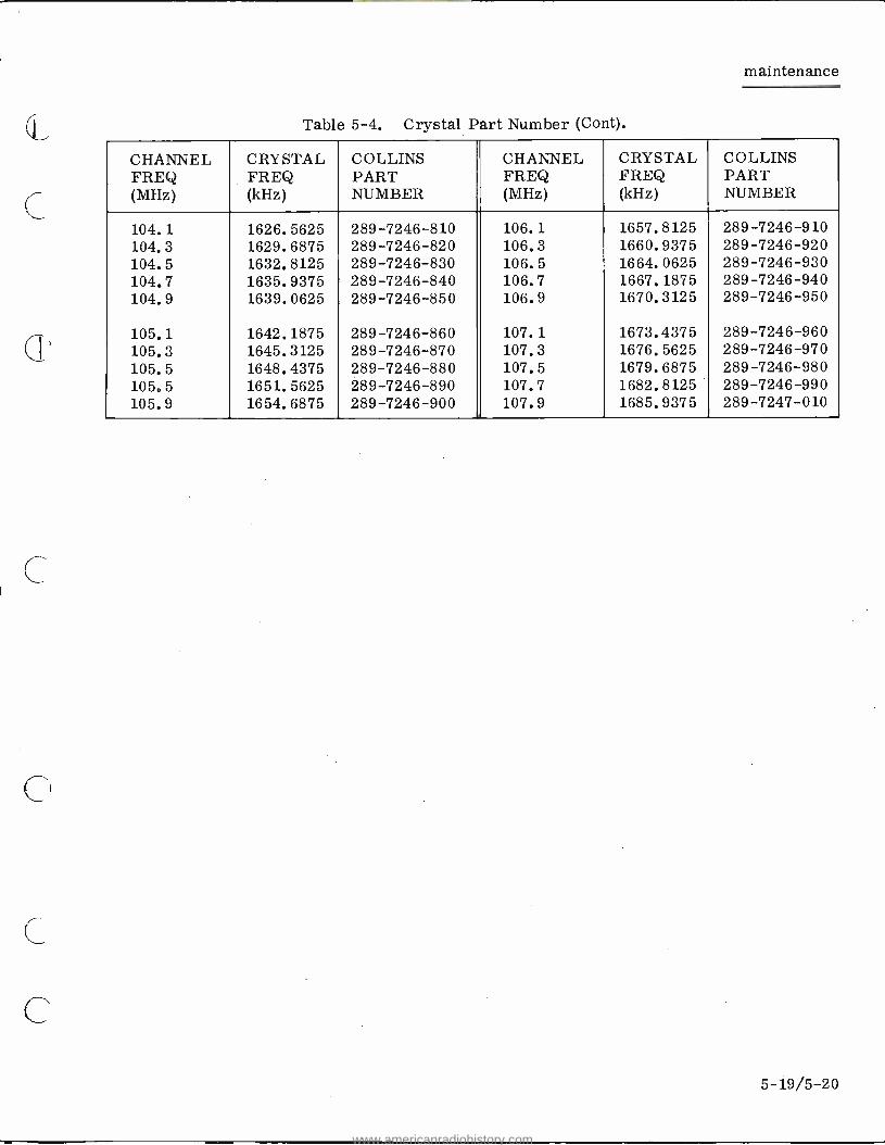
maintenance
Table 5 -4. Crystal Part Number (Cont).
CHANNEL FREQ (MHz)
CRYSTAL FREQ (kHz)
COLLINS PART NUMBER
CHANNEL FREQ (MHz)
CRYSTAL FREQ (kHz)
COLLINS PART NUMBER
104.1 1626.5625 289 -7246 -810 106.1 1657.8125 289 -7246 -910 104.3 1629.6875 289 -7246 -820 106.3 1660.9375 289 -7246 -920 104.5 1632.8125 289 -7246 -830 106.5 1664.0625 289 -7246 -930 104.7 1635.9375 289 -7246 -840 106.7 1667.1875 289 -7246 -940 104.9 1639.0625 289 -7246 -850 106.9 1670.3125 289 -7246 -950
105.1 1642.1875 289 -7246 -860 107.1 1673.4375 289 -7246 -960 105.3 1645.3125 289 -7246 -870 107.3 1676.5625 289 -7246 -970 105.5 1648.4375 289 -7246 -880 107.5 1679.6875 289 -7246 -980 105.5 1651.5625 289 -7246 -890 107.7 1682.8125 289 -7246 -990 105.9 1654.6875 289 -7246 -900 107.9 1685.9375 289 -7247 -010
5- 19/5 -20
www.americanradiohistory.com


Section 6
Parts List
6.1 GENERAL
This section provides parts lists and parts locations for all electrical components of the 310Z -2 FM Exciter. Figures 6 -1 through 6 -3 provide general views of the 310Z -2 FM Exciter with various access panels removed. The remaining figures with their corresponding parts lists identify all electrical components. These figures and parts lists are in order according to assembly reference designation.
6.2 ORDERING REPLACEMENT PARTS
Refer to the information inside the front cover for instructions on how to order replacement parts.
6 -1
www.americanradiohistory.com
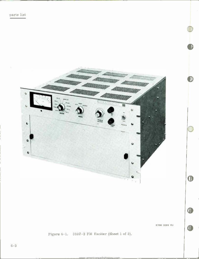
parts list
,
Figure 6-1. 310Z-2 FM Exciter (Sheet 1 of 3).
6-2
B700 3285 Rp
www.americanradiohistory.com

Figure 6-2. 310Z-2 FM Exciter (Sheet 2 of 3).
parts list
B700 3283 Rp
6-3
www.americanradiohistory.com

parts list
MOD OttT
éa OLIT
MODE POWER ADJUST
PA
POWER aase
PC1ihFR
Figure 6 -3. 310Z -2 FM Exciter (Sheet 3 of 3).
6-4
lpl
B700 3284 Rp
www.americanradiohistory.com

parts list
SYMBOL DESCRIPTION COLLINS
PART NUMBER
310Z -2 FM EXCITER 62?- 2184 -001
EXTENDER BOARD 791 -5365 -001 Al SCA GENERATOR 786W -1 772- 5338-001 A2 SCA GENERATOR 786W -1 772 5338 -001
A3 STL INTERFACE 785E -1 627- 2374 -001
A3 STEREO GENERATOR 786V -1 783- 6648 -001 A4 MODULATOR /EXCITER 627 -6695 -001
45 POWER AMPLIFIER 769 -0830 -001 A6 AUDIO /MTR REGULATOR 627- 9773 -001 81 BLOWER 009 -1829 -030
Cl CAPACITOR 3900UF 50 V 183 -1779 -370
C2 CAPACITOR 3900UF 50 V 183 1278 -370
Ci CAPACITOR 1000PF 500 V 913 -1292 -000 C4 CAPACITOR 100011F 50 V 183- 1282 -140
C5 CAPACITOR 1000UF 50 V 183 1282 -140 C6 CAPACITOR 1000UF 50 V 183 -1282 -140 C7 CAPACITOR 1000PF 500 V 913- 1292 -000
C8 CAPACITOR 1000PF 500 V 911 1292 -000 C9 CAPACITOR 1000PF 500 V 913- 1292 -000
C1D CAPACITOR 1000PF 500 V 913 1292 -000
C11 CAPACITOR 1000PF 500 V 913- 1292 -000 C12 CAPACITOR 1000PF 500 V 913 1292 -000 C13 CAPACITOR 1000PF 500 V 913- 1292 -000
C14 CAPACITOR 1000PF 500 V 913 1292 -000 C15 CAPACITOR 1000PF 500 V 913- 1292 -000
C16 CAPACITOR 1000PF 500 V 913 1297 -000
C17 CAPACITOR 1000PF 500 V 913- 1292 -000 C18 CAPACITOR O.IUF 200 V 913- 3681 -000 C19 CAPACITOR 0.1UF 200 V 913 3681 -000
C20 CAPACITOR 0.IUF 200 V 913 -3681 -000 C21 CAPACITOR 100PF 500 V 912- 2816 -000 CRI DIODE 1N1202 153 -1889 -000 CR2 DIODE 1N1202 353 1889 -000
CR3 DIODE 1N1202 353 -1889 -000 CR4 DIODE 1N1202 353 1889 -000 CR5 DIODE 1N4003 353- 6442 -030 CR6 DIODE 1N4003 353 6442 -030 CR7 DIODE 1N4003 353- 6442 -030 CR8 DIODE 1N4003 353 6442-030 El TERMINAL 547 -5305 -002 E2 TERMINAL 304- 2800 -000
E3 TERMINAL 304 2800 -000 E4 TERMINAL 304- 2800 -000 E5 TERMINAL 304 2800 -000 E6 TERMINAL 304 -2800 -000 E7 TERMINAL 304 2800 -000 ER TERMINAL 304 -0116 -000 E9 TERMINAL 304 0116 -000 EID TERMINAL 304 -1089 -000 E11 TERMINAL 304 -0116 -000 E12 TERMINAL 304 0116 -000 F1 FUSE 2ASB 264- 0297 -000 F2 FUSE 3A 264- 0928 -050 FL1 FILTER, LP 673- 1162 -020 HT1 HEATSINK 015- 3612 -010 HT2 HEATSINK 015- 3612 -020 J1 CONNECTOR 365- 0034 -000 J2 BNC CONNECTOR 357- 9248 -010 J3 BNC CONNECTOR 357 9248 -010 J4 BNC CONNECTOR 357 -9248 -010 J5 CONNECTOR 357 -7109 -000 J6 CONNECTOR 357 7109 -000 J7 CONNECTOR 357- 7109 -000 P? TNC CONNECTOR 357- 9666 -000 P3 TNC CONNECTOR 357 9666 -000 P4 TNC CONNECTOR 357- 9666 -000 QL TRANSISTOR 2N3054 352- 0581 -010
6 -5
www.americanradiohistory.com

parts list
SYMBOL DESCRIPTION COLLINS
PART NUMBER
02 TRANSISTOR 2N3055 352- 0583 -010 R1 RESISTOR, VARIABLE 5 K 376 -?4R7 -000 R2 RESISTOR, VARIABLE 10 K 380 -2264 -000 R3 RESISTOR 0.1 3 W 747 -5115 -000 R4 RESISTOR 68.1 K 1 W 705 -7184 -000 RS RESISTOR 1.5 10 W 747 -8531 -000 R6 RESISTOR 10 10 W 747- 8954 -000 R7 RESISTOR 10 10 W 747 -8954 -000
RR RESISTOR 22 1 W 745 -3282 -000 R9 RESISTOR 3.83 K 1/2 W 705- 7124 -000 RIO RESISTOR 464 1/2 W 705- 7090 -0Ó0 R11 RESISTOR 2700 1 W 745- 3370 -000 R12 RESISTOR 2.2 K 1/4 W 745 -0761 -000 R13 RESISTOR 47 K 1/4 W 745 -OR09 -000 SI SWITCH 266- 5376 -010 S2 SWITCH MODE 359- 9475 -130 SI SWITCH METER 359- 9475 -310 TI TRANSFORMER POWER 662 -0318 -010 TRl TERMINAL BOARD 367- 0024 -000 UI REGULATOR 7824KC 351 -1120 -040 IJ2 REGULATOR 7824KC 351 1120 -040 XF1 FUSEHOLDER 265- 1171 -000 XF2 FUSEHOLDER 265 1171 -000 XFL1 SOCKET 220- 1005 -000 X01 SOCKET TO -66 220 -0968 -020 XQ? SOCKET TO -3 220- 0968 -010 XU1 SOCKET TO -3 220 0968 -010 XU2 SOCKET TO -3 220- 0968 -010
6 -6
www.americanradiohistory.com
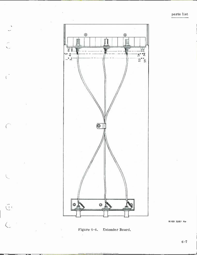
Figure 6 -4. Extender Board.
parts list
B700 3267 Rp
6 -7
www.americanradiohistory.com

parts list
SYMBOL DESCRIPTION COLLINS
PART NUMBER
EXTENDER BOARD 781 -5365 -001
JI CONNECTOR 357 -9210 -000 J2 CONNECTOR 357 9210 -000 J3 CONNECTOR 357- 9210 -000 J4 CONNECTOR 357- 9211 -000 J5 CONNECTOR 357 9211 -000 J6 CONNECTOR 357 -9211 -000 J7 CONNECTOR 372- 2426 -010 J8 CONNECTOR 372 2426 -010 J9 CONNECTOR 372- 7426 -010 J ID CONNECTOR 372 2426 -010 J11 CONNECTOR 372 -7426 -010 J12_ CONNECTOR 372 2426 -010 J13 CONNECTOR 372- 2426 -010 J14 CONNECTOR 372 2426 -010 JI5 CONNECTOR 372- 2426 -010 J16 CONNECTOR 372 2426 -010 J17 CONNECTOR 372 -2426 -010 J18 CONNECTOR 372 2426 -010 J19 CONNECTOR 372 -2426 -010 J20 CONNECTOR 372 2426 -010
6 -8
www.americanradiohistory.com
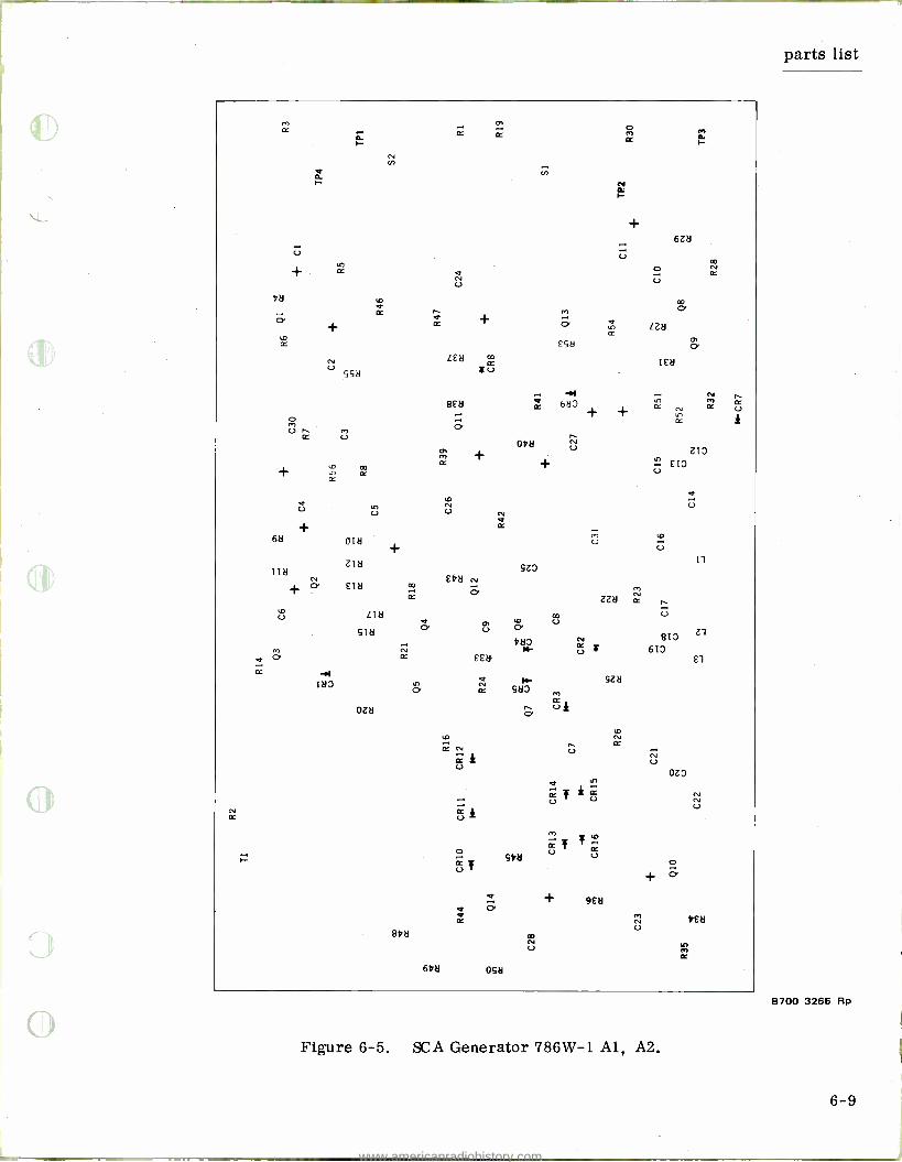
CC
U
+
d
CC
+
U SSa
6J
+
U
+
CO
oIa
ZI8
EI8
cc
N N
LEa s U
8E8
)O O N U U N c
L
518
oZ8
+
CC
c a
¢
8va
cc
Eva N
o+ U
E Ed
O N a CC
61.11
K N
U
N
d
+ 6Za
U a0
o N
U
co
LZa cc
ESa ° a IEa
N n 6a N
i ova CV
Z
+ Lc, EI0 U
O U
O U
U Il
5Z0
re,
zza dp U
t0 U a Zl 480 N sio IF
cc ; 610 El
U
i U U
`° Q
51.8 " U U
" + 9£8 a o' O CC
058
5Za
M N U
CZ;
U OZ0
N U
1.E8
Figure 6 -5. SCA Generator 786W -1 Al, A2.
parts list
B700 3265 Rp
6 -9
www.americanradiohistory.com

parts list
SYMBOL DESCRIPTION COLLINS
PART NUMBER
SCA GENERATOR 786W -1 Al, A2 772 -5338 -001
C1 CAPACITOR 6.8UF 35 V 184- 6216 -000 C2 CAPACITOR 6.8UF 35 V 184 6216 -000 C3 CAPACITOR 0.022ÚF 50 V 933 -0858 -000 C4 CAPACITOR 6.8UF 35 V 184- 6216 -000 C5 CAPACITOR 250UF 40 V 183- 2355 -150 C6 CAPACITOR 6.8UF 35 V 184 -6216 -000 C7 CAPACITOR 3900PF 500 V 912- 3046 -000 C8 CAPACITOR 3900PF 500 V 912 3046 -000 C9 CAPACITOR 6.8UF 35 V 184- 6216 -000 C10 CAPACITOR 2PF 500 V 916 -0076 -000 CII CAPACITOR 6.8UF 35 V 184 -6216 -000 C12 CAPACITOR 500UUF 500 V 912 -2977 -000 C13 CAPACITOR 100PF 500 V 912 -2816 -000 C14 CAPACITOR 47PF 500 V 912- 2792 -000 C15 CAPACITOR 5PF 500 V 916- 0118 -000 C16 CAPACITOR 820PF 500 V 912- 2995 -000 Cl? CAPACITOR 22PF 500 V 912 -2768 -000 C18 CAPACITOR 120PF 500 V 912 -2822 -000 C19 CAPACITOR 18PF 500 V 912-2763 -000 C20 CAPACITOR 470PF 500 V 912- 2974 -000 C21 CAPACITOR 47PF 500 V 912- 2792 -000 C22 CAPACITOR 0.0075UF 75 V 184 -9062 -040 C23 CAPACITOR 0.033UF 100 V 184- 6326 -580 C24 CAPACITOR 22ÚF 50 V 184 -6257 -000 C25 CAPACITOR 250UF 40 V 183- 2355 -150 C26 CAPACITOR 47UF 35 V 184 -6231 -000 C27 CAPACITOR 5UF 50 V 183- 1162 -000 C28 CAPACITOR 6.8UF 35 V 184- 6216 -000 C29 NOT USED C30 CAPACITOR 15UF 35 V 184- 6222 -000 C31 CAPACITOR 220UF 25 V 183 -2338 -000 CRI DIODE 1N914 353 -2906 -000 CR2 DIODE 1N995 353- 2042 -000 CR3 DIODE 1N995 353 2042 -000 CR4 DIODE 1N995 353- 2042 -000 CR5 DIODE 1N995 353 2042 -000 CR6 NOT USED CR7 DIODE 1N995 353- 2042 -000 CR8 DIODE 1N914 353 -2906 -000 CR9 DIODE 1N758 353- 2723 -000 CR10 DIODE 1N914 353 -2906 -000 CR11 DIODE 1N756A 353- 2983 -000 CR12 DIODE 1N756A 353 2983 -000 CR13 DIODE 1N914 353- 2906 -000 CR14 DIODE 1N914 353 2906 -000 CR15 DIODE 1N914 353 -2906 -000 CR16 DIODE 1N754Á 353- 2981 -000 El TERMINAL 306- 2222 -100 E2 TERMINAL 306 2222 -100 E3 TERMINAL 306 -2222 -100 LI INDUCTOR 5000UH 240 -0843 -000 L2 INDUCTOR 1000UH 240 -0839 -000 L3 INDUCTOR 5000UH 240 -0843 -000 01 TRANSISTOR 2N3569 352- 0629 -030 02 TRANSISTOR 2N3565 352- 0638 -010 Q3 TRANSISTOR 2N718Á 352- 0318 -000
04 TRANSISTOR 2N3638A 352- 0636 -020 Q5 TRANSISTOR 2N3638A 352 0636 -020 Q6 TRANSISTOR 2N3563 352 -0630 -010 Q7 TRANSISTOR 2N3563 35? 0630 -010 Q8 TRANSISTOR 2N3563 352 -0630 -010 09 TRANSISTOR 2N3646 352- 0680 -010
Q10 TRANSISTOR 2N3565 352 -0638 -010 011 TRANSISTOR 2N3643 352 -0713 -030 012 TRANSISTOR 2N3643 352 0713 -030 013 TRANSISTOR 2N3643 352 -0713 -030
6 -10
www.americanradiohistory.com
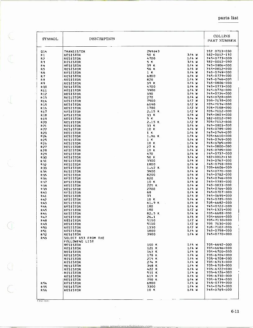
parts list
SYMBOL DESCRIPTION COLLINS
PART NUMBER
014 TRANSISTOR 2N3643 352 0713 -030 R1 RESISTOR 50 K 3/4 W 382 -0012 -130 R2 RESISTOR 4700 1/4 W 745- 0773 -000 R3 RESISTOR 5 K 3/4 W 382- 0012 -090 R4 RESISTOR 39 K 1/4 W 745 -0806 -000 R5 RESISTOR 56 K 1/4 W 745- 0812 -000 R6 RESISTOR 1 K 1/4 W 745- 0749 -000 R7 RESISTOR 6800 1/4 W 745- 0779 -000 R8 RESISTOR 820 1/4 W 745 -0746 -000 R9 RESISTOR 39 K 1/4 W 745- 0806 -000 R10 RESISTOR 4700 1/4 W 745- 0773 -000 R11 RESISTOR 3900 1/4 W 745 -0770 -000 R12 RESISTOR 390 1/4 W 745- 0734 -000 R13 RESISTOR 270 1/4 W 745- 0728 -000 R14 RESISTOR 7500 1/2 W 705- 7138 -000 R15 RESISTOR 6190 1/2 W 705- 7134 -000 R16 RESISTOR 1780 1/2 W 705 -7108 -000 R17 RESISTOR 2.15 K 1/2 W 705 -7112 -000 R18 RESISTOR 33 K 1/4 W 745- 0803 -000 R19 RESISTOR 5 K 3/4 W 382- 0012 -090 R20 RESISTOR 2.15 K 1/2 W 705 -7112 -000 R21 RESISTOR 33 K 1/4 W 745- 0803 -000 R22 RESISTOR 10 K 1/4 W 745- 0785 -000 R23 RESISTOR 1 K 1/4 W 745- 0749 -000 R24 RESISTOR 1.96 K 1/4 W 705- 6610 -000 R25 RESISTOR 1 K 1/4 W 745- 0749 -000 R26 RESISTOR 10 K 1/4 W 745- 0785 -000 R27 RESISTOR 27 K 1/4 W 745- 0800 -000 R28 RESISTOR 10 K 1/4 W 745- 0785 -000 R29 RESISTOR 470 1/4 W 745- 0737 -000 R30 RESISTOR 50 K 3/4 K 382- 0012 -130 R31 RESISTOR 3300 1/4 W 745- 0767 -000 R32 RESISTOR 1800 1/4 W 745 -0758 -000 R33 RESISTOR 1.62 K 1/4 W 705- 6606 -000 R34 RESISTOR 3900 1/4 W 745- 0770 -000 R35 RESISTOR 8200 1/4 W 745- 0782 -000 R36 RESISTOR 820 1/4 W 745- 0746 -000 R37 RESISTOR 10 K 1/4 W 745 -0785 -000 R38 RESISTOR 220 K 1/4 W 745 -0833 -000 R39 RESISTOR 2700 1/4 W 745- 0764 -000 R40 RESISTOR 68 1/4 W 745- 0707 -000 R41 RESISTOR 33 1/4 W 745- 0695 -000 R42 RESISTOR 10 K 1/4 W 745- 0785 -000 R43 RESISTOR 61.9 K 1/4 W 705- 6682 -000 R44 RESISTOR 180 1/4 W 745- 0722 -000 R45 RESISTOR 180 1/2 W 745- 1321 -000 R46 RESISTOR 82.5 K 1/4 W 705- 6688 -000 R47 RESISTOR 26.1 1/4 W 705- 6664 -000 R48 RESISTOR 5110 1/2 W 705 -7130 -000 R49 RESISTOR 5110 1/2 W 705 7130 -000 R50 RESISTOR 1330 1/2 W 705- 7102 -000 R51 RESISTOR 1800 1/4 W 745 -0758 -000 R52 RESISTOR 3900 1/4 W 745 -0770 -000 R53 SELECT R53 FROM THE
FOLLOWING LIST RESISTOR 100 K 1/4 W 705- 6692 -000 RESISTOR 121 K 1/4 W 705 -6696 -000 RESISTOR 147 K 1/4 W 705- 6700 -000 RESISTOR 178 K 1/4 W 705- 6704 -000 RESISTOR 215 K 1/4 W 705 -6708 -000 RESISTOR 274 K 1/4 W 705- 6713 -000 RESISTOR 348 K 1/4 W 705- 6718 -000 RESISTOR 422 K 1/4 W 705- 6722 -000 RESISTOR 511 K 1/4 W 705- 6726 -000 RESISTOR 619 K 1/4 W 705- 6730 -000 RESISTOR 750 K 1/4 W 705- 6734 -000
R54 RESISTOR 6800 1/4 W 745- 0779 -000 R55 RESISTOR 3300 1/4 W 745- 0767 -000 R56 RESISTOR 10 K 1/4 W 745 -0785 -000
6 -11
www.americanradiohistory.com

parts list
SYMBOL DESCRIPTION COLLINS
PART NUMBER
Si SWITCH, TOGGLE 266 -5321 -980 S2 SWITCH, TOGGLE 266 5321 -980 Ti TRANSFORMER, AF 667 -0187 -020 TP1 JACK, TIP 360- 0434 -100 TP2 JACK, TIP 360 0434 -100 TP3 JACK, TIP 360- 0434 -100 TP4 JACK, TIP 360- 0434 -010
6 -12
www.americanradiohistory.com
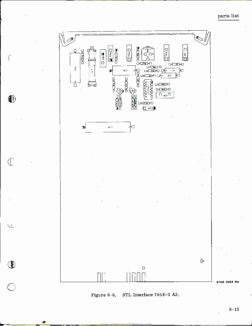
Er{
LJ
O
n
6
O
n a
O E
ñ
O
r tt
A
oia
Figure 6 -6. STL Interface 785E -1 A3.
parts list
B700 3264 Rp
6 -13
www.americanradiohistory.com
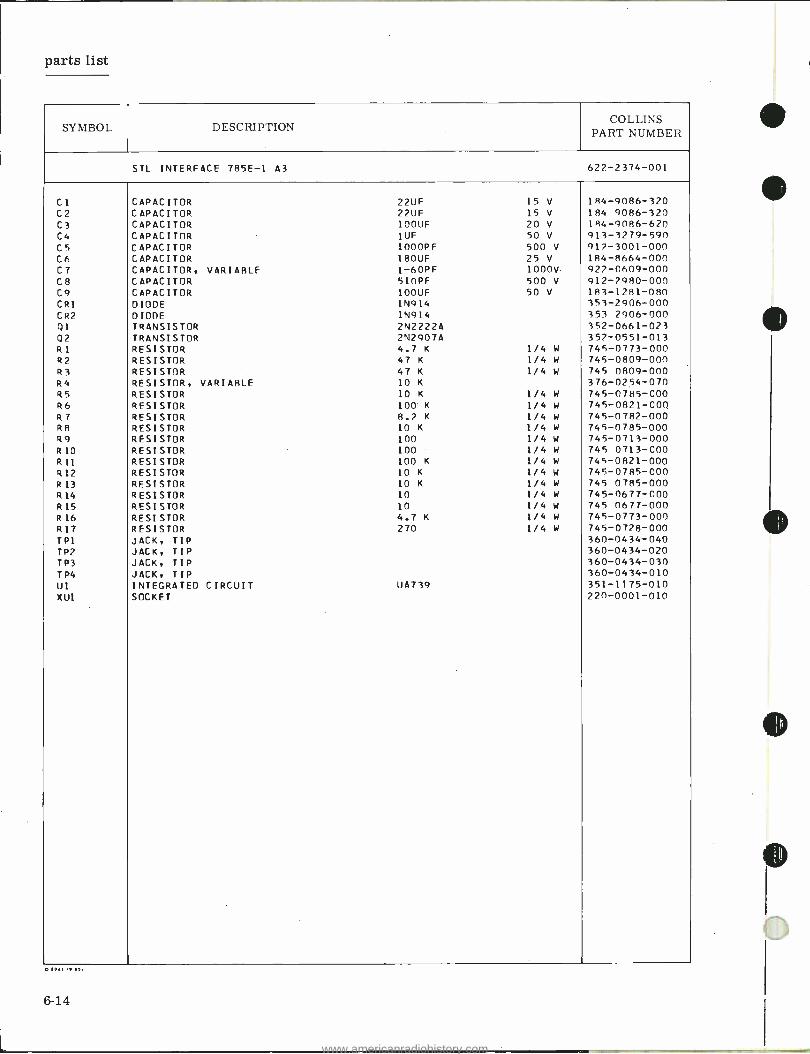
parts list
SYMBOL DESCRIPTION COLLINS
PART NUMBER
STL INTERFACE 785E -1 A3 622- 2374 -001
CI CAPACITOR 22UF 15 V 184 -9086 -320 C2 CAPACITOR 22UF 15 V 184 9086 -320 C3 CAPACITOR 1000F 20 V 184- 9086 -620 C4 CAPACITOR IUF 50 V 913- 3279 -590 CS CAPACITOR 1000PF 500 V 912- 3001 -000 C6 CAPACITOR 180UF 25 V 184 -8664 -000 C7 CAPACITOR, VARIABLE 1 -60PF 1000V 922- 0609 -000 C8 CAPACITOR 510PF 500 V 912 -2980 -000 C9 CAPACITOR 1000F 50 V 183 -1281 -080 CRI DIODE 1N914 353- 2906 -000 CR2 DIODE 1N914 353 2906 -000 Ql TRANSISTOR 2N2222A 352 -0661 -023 02 TRANSISTOR 2N2907A 352- 0551 -013 R1 RESISTOR 4.7 K 1/4 W 745 -0773 -000 R2 RESISTOR 47 K 1/4 W 745 -0809 -000 R3 RESISTOR 47 K 1/4 W 745 0809 -000 R4 RESISTOR, VARIABLE 10 K 376- 0254 -070 R5 RESISTOR 10 K 1/4 W 745 -0785 -000 R6 RESISTOR 100 K 1/4 w 745- 0821 -000 R7 RESISTOR 8.2 K 1/4 W 745 -0782 -000 R8 RESISTOR 10 K 1/4 w 745 -0785 -000 R9 RESISTOR 100 1/4 W 745 -0713 -000 RID RESISTOR 100 1/4 W 745 0713 -000 RII RESISTOR 100 K 1/4 W 745 -0821 -000 R12 RESISTOR 10 K 1/4 w 745- 0785 -000 813 RESISTOR 10 K 1/4 w 745 0785 -000 R14 RESISTOR 10 1/4 W 745 -0677 -000 R15 RESISTOR 10 1/4 W 745 0677 -000 R16 RESISTOR 4.7 K 1/4 w 745- 0773 -000 R17 RESISTOR 270 1/4 W 745- 0728 -000 TPI JACK, TIP 360- 0434 -040 TP2 JACK, TIP 360- 0434 -020 TP3 JACK, TIP 360- 0434 -030 TP4 JACK, TIP 360- 0434 -010 UI INTEGRATED CIRCUIT 11A739 351 -1175 -010 XU1 SOCKET 220- 0001 -010
6 -14
www.americanradiohistory.com

EC.
z 8178
r
)o
cc 90 cc
88
Ota ZO
£0
43
tta
cV U
Sta
4121
U
+ S21
621 cc
+ 9Z0
T
m o'
n U
o K
+ lV
£18
tl
613
r))
ZIO
w £421
OZO
n a
Zlj lla
4Z0
o
z
SO ao o+
< OZ
01 á d 4Z21
á 9Z21
60
I421
ora
803
co U
In
180
IZO
9£8
L£a
8£a
SZa
o o
00 l 2 +
LZa
N U
r. m PI U U
t£M
OTO
iI0
4t0
SIO
oc
Figure 6 -7. Stereo Generator 786V -1 A3.
parts list
B700 3266 Rp
6 -15
www.americanradiohistory.com
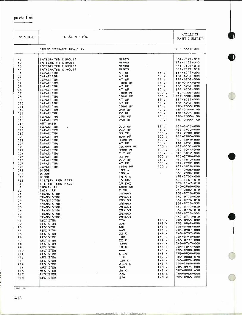
parts list
SYMBOL DESCRIPTION COLLINS
PART NUMBER
STEREO GENERATOR 786V -1 A3 783- 6648 -001
Al INTEGRATED CIRCUIT ML923 351- 7121 -010 A2 INTEGRATED CIRCUIT ML900 351 -7121 -030 A3 INTEGRATED CIRCUIT ML900 351 7121 -030 A4 INTEGRATED CIRCUIT M1923 351- 7121 -010 CI CAPACITOR 47 OF 35 V 184 -6231 -000 C2 CAPACITOR 47 OF 35 V 184 6231 -000 C3 CAPACITOR 47 OF 35 V 184 -6231 -000 C4 CAPACITOR 1000 OF 16 V 183- 2355 -090 C5 CAPACITOR 47 OF 35 V 184- 6231 -000 C6 CAPACITOR 47 OF 35 V 184 6231 -000 C7 CAPACITOR 1000 PF 500 V 912- 3001 -000 C8 CAPACITOR 1000 PF 500 V 912 3001 -000 C9 CAPACITOR 47 OF 35 V 184 -6231 -000 CIO CAPACITOR 47 OF 35 V 184 6231 -000 Cil CAPACITOR 1000 OF 16 V 183- 2355 -090 C12 CAPACITOR 250 OF 40 V 183- 2355 -150 C13 CAPACITOR 22 OF 35 V 184 -622.5 -000 C14 CAPACITOR 250 OF 40 V 183- 2355 -150 C15 CAPACITOR 250 OF 40 V 183 2355 -150 C16 NOT USED C17 CAPACITOR 2.2 OF 25 V 913 -3812 -000 CIA CAPACITOR 2.2 OF 25 V 913 3812 -000 C19 CAPACITOR 33 PF 500 V 912- 2780 -000 C20 CAPACITOR 820 PF 500 V 912- 2995 -000 C21 CAPACITOR 3300 PF 500 V 912- 3040 -000
C2? CAPACITOR 47 OF 35 V 184- 6231 -000 C23 CAPACITOR 30,000 PF 500 v 912- 3131 -000 C24 CAPACITOR 3900 PF 500 V 912 -3044 -000 C25 CAPACITOR 2.2 OF 25 V 913 -3812 -000 C26 CAPACITOR 33 PF 500 V 912 -2780 -000 C27 CAPACITOR 2.2 OF 25 V 913 -3812 -000 C28 CAPACITOR 47 PF 500 V 912 -2792 -000 C29 CAPACITOR 1800 PF 500 V 912 -3018 -000 CRI DIODE 1N914 353 -2906 -000 CR2 DIODE 1N914 353 2906 -000 CR3 DIODE 1N747A 353 -2702 -000 FL1 FILTER, LOW PASS 15 KHZ 673- 1167 -010 FL2 FILTER, LOW PASS 15 KHZ 673 1167 -010 LI CHOKE, RF 6800 UH 240 -2560 -000 L2 COIL, RF 2 MH 240 -0882 -010 01 TRANSISTOR 2N3643 352- 0713 -030 02 TRANSISTOR 2N3643 352 0713 -030 03 TRANSISTOR 2N3153 352- 0776 -010 04 TRANSISTOR 2N3643 35 ?- 0713 -030 05 TRANSISTOR 2N3643 352 0713 -030 06 TRANSISTOR 2N3153 352- 0776 -010 07 TRANSISTOR 2N3643 352 -0713 -030 08 TRANSISTOR 2N3643 352 0713 -030 RI RESISTOR 226 1/8 W 705- 0965 -000 R2 RESISTOR 226 1/8 W 705 0965 -000 R3 RESISTOR 681 1/8 w 705 -0988 -000 R4 RESISTOR 649 1/8 W 705- 0987 -000 R5 RESISTOR 22 K 1/4 W 745 -0797 -000 R6 RESISTOR 100 1/8 W 705- 0948 -000 R7 RESISTOR 22 K 1/4 W 745- 0797 -000 R8 RESISTOR 3300 1/4 W 745 -0767 -000 R9 RESISTOR 10 K 1/8 W 705- 1044 -000 RIO RESISTOR 464 1/8 W 705 -0980 -000 R11 RESISTOR 61.9 1/8 w 705- 0938 -000 R12 RESISTOR 1 K 1/2 W 382- 0008 -070 P13 RESISTOR 120 K 1/4 w 745- 0824 -000 R14 RESISTOR 21.5 K 1/8 W 705- 1060 -000 R15 RESISTOR 348 1/8 w 705- 0974 -000 R16 RESISTOR 20 K 1/2 w 382 -0008 -450 R17 RESISTOR 226 1/8 W 705- 0965 -000 R18 RESISTOR 226 1/8 w 705 0965 -000
6 -16
www.americanradiohistory.com
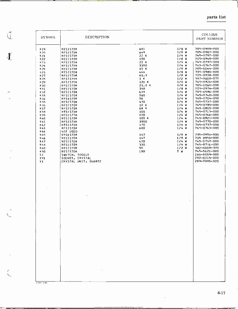
parts list
SYMBOL DESCRIPTION COLLINS
PART NUMBER
R19 RESISTOR 691 1/8 W 705 -0988 -000 R20 RESISTOR 649 1/8 W 705- 0987 -000 R21 RESISTOR 22 K 1/4 W 745 -0797 -000 R22 RESISTOR 100 1/8 W 705- 0948 -000 R23 RESISTOR 22 K 1/4 W 745- 0797 -000 R24 RESISTOR 3300 1/4 W 745- 0767 -000 R75 RESISTOR 10 K 1/8 W 705 -1044 -000 R ?6 RESISTOR 464 1/8 W 705- 0980 -000 R27 RESISTOR 61.9 1/8 W 705- 0938 -000 R28 RESISTOR 1 K 1/2 W 387 -0008 -070 P29 RESISTOR 120 K 1/4 W 745 -0824 -000 R30 RESISTOR 21.5 K 1/8 W 705- 1060 -000 R31 RESISTOR 348 1/8 W 705- 0974 -000 R32 RESISTOR 619 1/4 W 705 -6586 -000 R33 RESISTOR 560 1/4 W 745- 0740 -000 R34 RESISTOR 56 1/4 W 745- 0704 -000 R35 RESISTOR 470 1/4 W 745- 0737 -000 R36 RESISTOR 10 K 1/4 W 745 -0785 -000 R37 RESISTOR 68 K 1/4 W 745 -0815 -000 R38 RESISTOR 100 1/4 W 745 -0713 -000 R39 RESISTOR 820 1/4 W 745- 0746 -000 R40 RESISTOR 100 K 1/4 W 745- 0821 -000 R41 RESISTOR 3900 1/4 W 745- 0770 -000 R47 RESISTOR 470 1/4 W 745- 0737 -000 R43 RFSISTDR 680 1/4 W 745 -0743 -000 R44 NOT USED R45 RESISTOR 147 1/8 W 705- 0956 -000 R46 RESISTOR 147 1/8 W 705 0956 -000 R47 RESISTOR 470 1/4 W 745 -0737 -000 R48 RESISTOR 330 1/4 W 745- 0731 -000 R49 RESISTOR 50 1/2 W 382- 0008 -370 R50 RESISTOR 180 2 W 745 -5621 -000 Si SWITCH, TOGGLE 266 -5059 -000 XVI SOCKET, CRYSTAL 292 -0215 -000 YI CRYSTAL UNIT, QUARTZ 289- 7095 -020
6 -17
www.americanradiohistory.com

parts list
V
U
9 u
o
III2E1 a
00 N
.
rc Q jL o sLa
( Ob)a ` )
O121iM 1
co
Ó _ D-
,6) )
J O
0 á v
N
-90000000- )p 0 çnx/4n _ m
44 0)
r
O
O
O
Le
ce
6L27 NLJ ] LL70) OEä
O O O
' l J OS4a0
O Di G. IC Diu .6,,p0
(I657CD)
°)421 30 01423A Ml,10
co
Figure 6 -8. Modulator /Exciter A4 (Sheet 1 of 2).
6 -18
B700 3263 Rp
www.americanradiohistory.com

parts list
` ¡,J ¡
a)n
Figure 6 -9. Modulator /Exciter A4 (Sheet 2 of 2).
B700 3270 Rp
6 -19
www.americanradiohistory.com
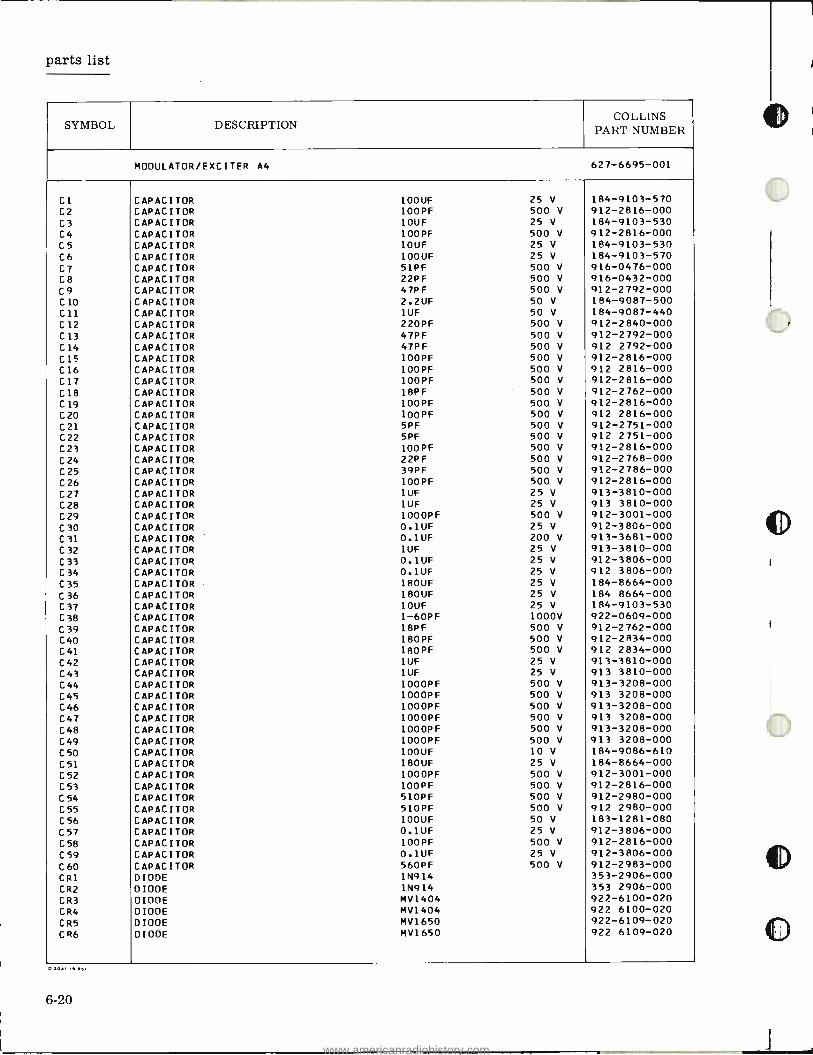
parts list
SYMBOL DESCRIPTION COLLINS
PART NUMBER
MODULATOR /EXCITER A4 627- 6695 -001
CI CAPACITOR 1000F 25 V 184- 9103 -570 C2 CAPACITOR 100PF 500 V 912- 2816 -000 C3 CAPACITOR IOUF 25 V 184- 9103 -530 C4 CAPACITOR 100PF 500 V 912 -2816 -000 C5 CAPACITOR 10UF 25 V 184- 9103 -530 C6 CAPACITOR 1000F 25 V 184- 9103 -570 C7 CAPACITOR 51PF 500 V 916 -0476 -000 CS CAPACITOR 22PF 500 V 916- 0432 -000 C9 CAPACITOR 47PF 500 V 912- 2792 -000 CID CAPACITOR 2.2UF 50 V 184 -9087 -500 C11 CAPACITOR 1UF 50 V 184 -9087 -440 C12 CAPACITOR 220PF 500 V 912- 2840 -000 C13 CAPACITOR 47PF 500 V 912 -2792 -000 C14 CAPACITOR 47PF 500 V 912 2792 -000 C15 CAPACITOR 100PF 500 V 912 -2816 -000 C16 CAPACITOR 100PF 500 V 912 2816 -000 CI7 CAPACITOR 100PF 500 V 912- 2816 -000
C18 CAPACITOR I8PF 500 V 912- 2762 -000 C19 CAPACITOR 100PF 500 V 912- 2816 -000 C20 CAPACITOR 100PF 500 V 912 2816 -000 C21 CAPACITOR 5PF 500 V 912- 2751 -000 C22 CAPACITOR 5PF 500 V 912 2751 -000 C23 CAPACITOR 100PF 500 V 912 -2816 -000 C24 CAPACITOR 22PF 500 V 912- 2768 -000
C25 CAPACITOR 39PF 500 V 912- 2786 -000 C26 CAPACITOR 100PF 500 V 912 -2816 -000 C27 CAPACITOR IUF 25 V 913- 3810 -000 C28 CAPACITOR IUF 25 V 913 3810 -000 C29 CAPACITOR 1000PF 500 V 912- 3001 -000
C30 CAPACITOR 0.1UF 25 V 912- 3806 -000 C31 CAPACITOR 0.1UF 200 V 913- 3681 -000 C32 CAPACITOR 1UF 25 V 913- 3810 -000
C33 CAPACITOR 0.1UF 25 V 912 -3806 -000 C34 CAPACITOR 0.1UF 25 V 912 3806 -000 C35 CAPACITOR 180UF 25 V 184 -8664 -000
C36 CAPACITOR 180UF 25 V 184 8664 -000 C37 CAPACITOR IOUF 25 V 184- 9103 -530 C38 CAPACITOR 1 -60PF 1000V 922- 0609 -000
C39 CAPACITOR 18PF 500 V 912- 2762 -000 C40 CAPACITOR 180PF 500 V 912 -2834 -000 C41 CAPACITOR 180PF 500 V 912 2834 -000 C42 CAPACITOR 1UF 25 V 913- 3810 -000 C43 CAPACITOR IUF 25 V 913 3810 -000 C44 CAPACITOR 1000PF 500 V 913 -3208 -000 C45 CAPACITOR I000PF 500 V 913 3208 -000 C46 CAPACITOR 1000PF 500 V 913- 3208 -000 C47 CAPACITOR 1000PF 500 V 913 3208 -000 C48 CAPACITOR 1000PF 500 V 913- 3208 -000 C49 CAPACITOR 1000PF 500 V 913 3208 -000 C50 CAPACITOR 1000F IO V 184- 9086 -610 C51 CAPACITOR 180UF 25 V 184 -8664 -000 C52 CAPACITOR 1000PF 500 V 912 -3001 -000 C53 CAPACITOR 100PF 500 V 912- 2816 -000 C54 CAPACITOR 510PF 500 V 912 -2980 -000 C55 CAPACITOR 510PF 500 V 912 2980 -000
C56 CAPACITOR 1000F 50 V 183- 1281 -080 C57 CAPACITOR 0.1UF 25 V 912- 3806 -000 C58 CAPACITOR 100PF 500 V 912 -2816 -000 C59 CAPACITOR 0.1UF 25 V 912 -3806 -000
C60 CAPACITOR 560PF 500 V 912 -2983 -000 CRI DIODE 1N914 353- 2906 -000
CR2 DIODE 1N914 353 2906 -000
CR3 DIODE MV1404 922- 6100 -020 CR4 DIODE MV1404 922 6100 -020
CR5 DIODE MV1650 922- 6109 -020
CR6 DIODE MV1650 922 6109 -020
6 -20
www.americanradiohistory.com

parts list
SYMBOL DESCRIPTION COLLINS
PART NUMBER
CR7 DIODE 1N914 353- 2906 -000 CR8 DIODE 1N914 353 2906 -000
CR9 DIODE 1N914 353 -2906 -000 CR10 DIODE 1N914 353 2906 -000
CR11 DIODE 1N914 353 -2906 -000 CR12 DIODE 1N914 353 2906 -000
CR13 DIODE 1N914 353- 2906 -000
CR14 DIODE 1N914 353 2906 -000
CR15 DIODE 1N914 353 -2906 -000 CR16 DIODE 353 -3725 -060 CR17 DIODE 1N914 353 -2906 -000 CR18 DIODE 1N5159 353- 6549 -020
CR19 DIODE 1N914 353- 2906 -000 HS01 HEATSINK 352- 2619 -030 HS02 HEATSINK 352 2619 -030
L1 INDUCTOR 1.5 UHY 240- 2715 -150
L? INDUCTOR 1.5 UHY 240 2715 -150 L3 INDUCTOR 1.5 UHY 240- 2715 -150 L4 INDUCTOR 1.5 UHY 240 2715 -150 L5 INDUCTOR, VARIABLE 0.13 UHY 242 -0424 -050 L6 INDUCTOR 0.47 UHY 240 -2715 -090 L7 INDUCTOR 1.5 UHY 240- 2715 -150 LA INDUCTOR 0.1 UHY 240- 2715 -010 L9 INDUCTOR 10 HY 678- 0205 -010 L10 INDUCTOR 150 MHY 240 -0276 -000 M1 METER 0 -50 UA 458- 0908 -020 P1 CONNECTOR BOARD 627- 9766 -001 P2 CONNECTOR 357 -9210 -000 01 TRANSISTOR 2N5109 352- 0766 -010 02 TRANSISTOR 2N5109 352 0766 -010
03 TRANSISTOR 2N2907Á 352- 0551 -013 Q4 TRANSISTOR 2N2222A 352- 0661 -023
05 TRANSISTOR 2N2222A 352 0661 -023
06 TRANSISTOR 2N2222A 352- 0661 -023 07 TRANSISTOR 2N2222A 352 0661 -023 08 TRANSISTOR 2N2222A 352- 0661 -023 09 TRANSISTOR 2N2222A 352 0661 -023 010 TRANSISTOR 2N2222A 352- 0661 -023 011 TRANSISTOR 2N3053 352- 0613 -010 R1 RESISTOR, VARIABLE 500 376- 0254 -030 R2 RESISTOR 100 1/4 W 745 -0713 -000 R3 RESISTOR 22 K 1/4 W 745- 0797 -000 R4 RESISTOR 47 K 1/4 W 745- 0809 -000 R5 RESISTOR, VARIABLE 25 K 380- 3761 -080 R6 RESISTOR 22 K 1/4 W 745- 0797 -000 R7 RESISTOR, VARIABLE 10 K 3/4 W 381 -1802 -000 R8 RESISTOR 22 K 1/4 W 745- 0797 -000 R9 RESISTOR 22 K 1/4 W 745 0797 -000 RIO RESISTOR 10 K 1/4 W 745- 0785 -000 RII RESISTOR 4.7 K 1/4 W 745- 0773 -000 R12 RESISTOR 1 K 1/4 W 745- 0749 -000 R13 RESISTOR 10 K 1/4 W 745- 0785 -000 R14 RESISTOR 8.2 K 1/4 W 745- 0782 -000 R15 RESISTOR 47 K 1/4 W 745- 0809 -000 R16 RESISTOR 470 K 1/4 W 745- 0845 -000 R17 RESISTOR 100 1/2 W 745 -1310 -000 R18 RESISTOR 15 1/4 W 745- 0683 -000 R19 RESISTOR 68 1/4 W 745- 0707 -000 R20 RESISTOR 15 1/4 W 745 -0683 -000 R21 RESISTOR 150 1 W 745 -3317 -000 R22 RESISTOR 3.3 K 1/4 W 745- 0767 -000 R23 RESISTOR 470 1/4 W 745 -0737 -000 R24 RESISTOR 47 1/2 W 745 -1296 -000 R25 RESISTOR 4.7 K 1/4 W 745 -0773 -000 R26 RESISTOR 22 1/2 W 745- 1282 -000 R27 RESISTOR 22 1/? W 745 1282 -000 R28 RESISTOR 47 1/2 W 745 -1296 -000 R29 RESISTOR 3.9 K 1/4 W 745- 0770 -000 R30 RESISTOR 1.2 K 1/4 W 745- 0752 -000
6 -21
www.americanradiohistory.com

parts list
SYMBOL DESCRIPTION COLLINS PART NUMBER
R31 RESISTOR 470 1/4 W 745- 0737 -000 R32 RESISTOR 100 1/4 W 745- 0713 -000 R33 RESISTOR 270 1/4 W 745- 0728 -000 R34 RESISTOR 1 K 1/4 W 745- 0749 -000 R35 RESISTOR 220 1 W 745 -3324 -000 R36 RESISTOR 10 K 1/4 W 745- 0785 -000 R37 RESISTOR 10 K 1/4 W 745 0785 -000 R38 RESISTOR 1 K 1/4 W 745- 0749 -000 R39 RESISTOR 10 K 1/4 W 745- 0785 -000 R40 RESISTOR 2.2 K 1/2 W 745 -1366 -000 R41 RESISTOR 2.2 K 1/4 W 745- 0761 -000 R42 RESISTOR 470 1/4 W 745- 0737 -000 R43 RESISTOR 4.7 K 1/4 W 745 -0773 -000 R44 RESISTOR 1 K 1/4 W 745 - 0749 -000 R45 RESISTOR 2.7 K 1/4 W 745- 0764 -000 R46 RESISTOR 1 K 1 W 745 -3352 -000 R47 RESISTOR 4.7K 1/4 W 745 -0773 -000 R48 RESISTOR 1 K 1/4 W 745- 0749 -000 R49 RESISTOR 2.7 K 1/2 W 745- 1370 -000 R50 RESISTOR 39 2 W 745- 5593 -000 R51 RESISTOR 100 K 1/4 W 745- 0821 -000 R52 RESISTOR 1 K 1/4 W 745- 0749 -000 R53 RESISTOR IO K 1/4 W 745- 0785 -000 R54 RESISTOR 10 K 1/4 W 745 0785 -000 R55 RESISTOR 4.7 K 1/4 W 745 -0773 -000 R56 RESISTOR 15 1/4 W 745- 0683 -000 R57 RESISTOR 10 K 1/4 W 745- 0785 -000 R58 RESISTOR 10 K 1/4 W 745 0785 -000 R59 RESISTOR 270 1/4 W 745- 0728 -000 R60 RESISTOR 470 1/4 W 745- 0737 -000 R61 RESISTOR 470 1/4 W 745 0737 -000 R62 RESISTOR 1 K 1/4 W 745- 0749 -000 R63 RESISTOR 1 K 1/4 W 745 0749 -000 R64 RESISTOR 27 K 1/4 W 745- 0800-000 R65 RESISTOR 27 K 1/4 W 745 0800 -000 R66 RESISTOR 1 K 1/4 W 745- 0749 -000 R67 RESISTOR 100 1/4 W 745 -0713 -000 R68 RESISTOR 15 K 1/4 W 745- 0791 -000 R69 RESISTOR 1.2 K 1/2 W 745- 1356 -000 R70 RESISTOR 15 K 1/4 W 745 -0791 -000 R71 RFSISTOR 2.2 K 1/4 W 745- 0761 -000 R72 RESISTOR 4.7 K 1/4 W 745- 0773 -000 R73 RESISTOR 2.2 K 1/4 W 745- 0761 -000 R74 RESISTOR 2.2 K 1/4 W 745 0761 -000 R75 RESISTOR 15 K 1/4 W 745- 0791 -000 St SWITCH 266- 5321 -990 UI INTEGRATED CIRCUIT MC10178 351- 1520 -020 U2 INTEGRATED CIRCUIT CD4020 351- 8159 -090 U3 INTEGRATED CIRCUIT C04027 351 -8159 -180 U4 INTEGRATED CIRCUIT CD4024 351- 8159 -100 U5 INTEGRATED CIRCUIT CA3018 351 -1016 -010 U6 INTEGRATED CIRCUIT 7805KC 351- 1120 -080 VR1 ZENER DIODE 1N4744A 353- 6481 -330 VR2 ZENER DIODE 1N4744A 353 6481 -330 VR3 ZENER DIODE 1N4740A 353- 6481 -250 XCR16 RING, RETAINING 353 -3725 -060 XU1 SOCKET 220 -0001 -020 XU2 SOCKET 220 0001 -020 XU3 SOCKET 220- 0001 -020 XU4 SOCKET 220 -0001 -010 XU5 INSULATOR DISC 352 -9552 -040 XY1 OVEN CRYSTAL 292 -0328 -010
6 -22
www.americanradiohistory.com

parts list
J
Figure 6 -10. Power Amplifier A5.
8700 3268 Rp
6. -23
www.americanradiohistory.com

parts list
SYMBOL DESCRIPTION COLLINS
PART NUMBER
POWER AMPLIFIER A5 769- 0830 -001
Cl CAPACITOR 680PF 1000V 913- 1194 -000 C2 CAPACITOR 470PF 500 V 913- 1189 -000 C3 CAPACITOR 470PF 500 V 913 1189 -000 C4 CAPACITOR 0.01UF 100 V 913 -3680 -000 C5 CAPACITOR 1000PF 500 V 912- 4115 -330 C6 CAPACITOR 15PF 500 V 912 -2759 -000 C7 CAPACITOR 15PF 500 V 912 2759 -000 C8 CAPACITOR 5.5 -18PF 350 V 917 -1222 -000 C9 CAPACITOR 33PF 500 V 912- 2781 -000 C10 CAPACITOR 0.01ÚF 100 V 913- 3680 -000 CII CAPACITOR 1000PF 500 V 912 -4115 -330 C12 CAPACITOR 10PF 500 V 912 -2753 -000 C13 CAPACITOR 18PF 500 V 912- 2762 -000 C14 CAPACITOR 5.5 -18PF 350 V 917- 1222 -000 C15 CAPACITOR 82PF 500 V 912 -2810 -000 C16 CAPACITOR 500PF 500 V 912- 0667 -000 C17 CAPACITOR 0.01ÚF 100 V 913 -3680 -000 CIR CAPACITOR 0.IPF 200 V 913- 3681 -000 C19 CAPACITOR 1000PF 500 V 912 -4115 -330 C20 CAPACITOR 110PF 500 V 912- 2819 -000 C21 CAPACITOR 27PF 500 V 912- 2774 -000 C22 CAPACITOR 5.5 -18PF 350 V 917- 1222 -000 C23 CAPACITOR 100PF 500 V 912- 2816 -000 C24 CAPACITOR 22PF 500 V 912- 2769 -000 CRI DIODE 1N914 353- 2906 -000 FL1 FILTER, RI 1300PF 200 V 241- 0332 -000 FL2 FILTER, RI 1300PF 200 V 241 0332 -000 FL3 FILTER, RI 1300PF 200 V 241 -0332 -000 JI CONNECTOR VG1051 357- 9210 -000 J2 CONNECTOR VG1051 357 9210 -000 LI COIL, RF 1 UH 240 -1590 -000 L2 COIL 0.082 UH 776 -1882 -001 L3 COIL 0.048 UH 776 -1910 -001 L4 COIL, RF 0.15 UH 240 -1585 -000 L5 COIL, RF 2.2 UH 240 -1654 -000 L6 COIL 0.056 UH 776 -1911 -001 L7 COIL 0.05 UH 776 -1912 -001 L8 CHOKE, RF 1.2 UH 240 -1605 -000 L9 COIL 0.092 UH 776 -1883 -001 L11 COIL, RF 0.15 UH 240 -1585 -000 01 TRANSISTOR 2N3866 352 -0671 -010 Q2 TRANSISTOR 2N3375 352- 0611 -010 03 TRANSISTOR 2N5102 352- 0747 -010 RI RESISTOR 39 1/2 W 745 -1293 -000 R2 RESISTOR 22 3 w 747 -5327 -000 R3 RESISTOR 23.7 1/2 W 705 -7018 -000 R4 RESISTOR 270 3 w 747- 5349 -000 R5 RESISTOR 10 1/4 W 705- 6500 -000 R6 RESISTOR 100 1/2 W 745 -1310 -000 R7 RESISTOR 2 1 w 747- 4230 -300 R11 RESISTOR 10 1/2 w 745- 1268 -000 R12 RESISTOR 0.5 2.5 w 746- 9457 -000 R13 RESISTOR 4.7 1/2 W 745- 6279 -000 R14 RESISTOR 10 1/2 W 745- 1268 -000 R15 RESISTOR 10 1/2 W 745 1268 -000 R16 RESISTOR 1 K 1/4 W 745- 0749 -000 R17 RESISTOR 470 1/4 W 745- 0737 -000
6 -24
www.americanradiohistory.com

á 3
Cf O O J
0
EJO
0
b'J EMI 1
O
m a o
DOD
te V
I NM IZIZI
CI
N r-
.1{N NL Sal
OEM
a
° Lb
17
C1
A
J o
3
d
+
o U
+ 67
SZa
vza Zla
0
L çd
33
3
3
3
Q
O
Q
0 O
Q
0
Q
Q
0 Q
Q
Q Q
Q Q Q
Q
O ç? CI
'cap oç3
6La
91.2
LZ3
3Q SL3
4L3
4La
LL3
OZ96,3Q
Q
n e,-¡Q
Q
11
.nia
Sia
1,13
U3
113
Ota
G34
La Q ..)a
43 Q b3 Q
Q Z3
3ci
6ç 3
93 cl «.O
Sç3
0
Figure 6 -11. Audio /Mtr Regulator A6.
parts list
B700 3269 Rp
6-25
www.americanradiohistory.com

parts list
SYMBOL DESCRIPTION COLLINS
PART NUMBER
AUDIO /MTR REGULATOR A6 627- 9773 -001
C1 CAPACITOR 22UF 15 V 184 -9086 -320 C2 CAPACITOR 180UF 25 V 184 -8664 -000 C3 CAPACITOR 22UF 15 V 184 -9086 -320 C4 CAPACITOR 0.1UF 25 V 913 -3806 -000 C5 CAPACITOR [OUF 20 V 184- 9086 -470 C6 CAPACITOR 150UF 30 V 184 -8673 -000 C7 CAPACITOR 22UF 15 V 184 -9086 -320 CM CAPACITOR 180UF 25 V 184 -8664 -000 C9 CAPACITOR 22UF 15 V 184- 9086 -320 CIO CAPACITOR 22UF 15 V 184 9086 -320 C11 CAPACITOR [OUF 20 V 184- 9086 -470 C12 CAPACITOR 100PF 500 V 912- 2816 -000 C13 CAPACITOR O.OIUF 50 V 913- 3279 -110 C14 CAPACITOR 22UF 15 V 184 -9086 -320 C15 CAPACITOR 22UF 15 V 184 9086 -320 C16 CAPACITOR 0.030UF 500 V 912 -3133 -000 C17 NOT USED C18 CAPACITOR 180UF 25 V 184 -8664 -000 C19 CAPACITOR 180UF 25 V 184 8664 -000 C20 NOT USED C21 CAPACITOR O.O30UF 500 V 912- 3133 -000 C22 CAPACITOR 22UF 15 V 184- 9086 -320 C23 CAPACITOR 0.0111F 50 V 913- 3279 -110 C74 CAPACITOR LUF 25 V 913- 3810 -000 C ?5 CAPACITOR 100PF 500 V 912- 2816 -000 C26 CAPACITOR 2200PF 500 V 913- 3025 -000 C27 CAPACITOR IUF 25 V 913- 3810 -000 C28 CAPACITOR 180UF 25 V 184- 8664 -000 C29 CAPACITOR 22UF 15 V 184- 9086 -320 C30 CAPACITOR 0.IUF 200 V 913- 3681 -000 Cu CAPACITOR 0.1UF 200 V 913 3681 -000 CR! DIODE 1N914 353- 2906 -000 CR2 DIODE 1N914 353 2906 -000 CR3 DIODE 1N4003 351-6442-030 CR4 DIODE 1N914 353- 2906 -000 CR5 DIODE 1N914 353 2906 -000 CR6 DIODE 1N914 353- 2906 -000 Kl RELAY 970 -2420 -040 LI INDUCTOR 6.R MHY 240 -1578 -000 01 TRANSISTOR 2N2907A 352 -0551 -013 Q2 TRANSISTOR 2N2907A 352 0551 -013 03 TRANSISTOR 2N2907A 352- 0551 -013 Q4 TRANSISTOR 2N2907A 352 0551 -013 05 TRANSISTOR 2N2907A 352 -0551 -013 06 TRANSISTOR 2N2907A 352 0551 -013 Q7 TRANSISTOR, SCR 2N4168 353 -6485 -020 08 TRANSISTOR 2N2222A 352- 0661 -023 09 TRANSISTOR 2N2222A 352 0661 -023 Q10 TRANSISTOR 2N3053 352- 0613 -010 RI RESISTOR 8.2 K 1/4 W 745 -0782 -000 R2 RESISTOR 47 K 1/4 W 745- 0809 -000 R3 RESISTOR 1.2 K 1/4 W 745- 0752 -000 R4 RESISTOR 82 1/4 W 745- 0710 -000 R5 RESISTOR 5.6 K 1/4 W 745- 0776 -000 R6 RESISTOR 8.2 K 1/4 W 745- 0782 -000 R7 RESISTOR 5.6 K l/4 W 745- 0776 -000 R8 RESISTOR 23.7 K ./4 W 705- 6662 -000 R9 RESISTOR 1.2 K L/4 W 745- 0752 -000 RIO RESISTOR, VARIABLE 100 380- 3761 -010 RI[ RESISTOR 390 K 1/4 W 745- 0842 -000 R12 RESISTOR 5.6 K 1/4 W 745- 0776 -000 R13 RESISTOR 1.2 K 1/4 W 745- 0752 -000 R14 RESISTOR 5.6 K 1/4 W 745- 0776 -000 R15 RESISTOR 3.9 K 1/4 W 745- 0770 -000 R16 RESISTOR 12 K 1/4 W 745- 0788 -000 RI7 RESISTOR 2.2 K 1/4 W 745- 0761 -000
6 -26
www.americanradiohistory.com
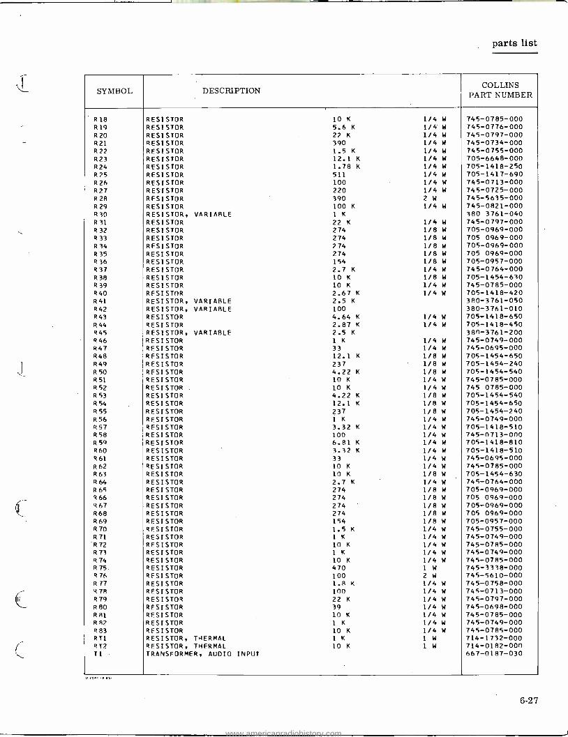
parts list
SYMBOL DESCRIPTION COLLINS
PART NUMBER
R18 RESISTOR 10 K 1/4 W 745 -0785 -000 R19 RESISTOR 5.6 K 1/4 W 745- 0776 -000 R20 RESISTOR 22 K 1/4 W 745- 0797 -000 R21 RESISTOR 390 1/4 W 745- 0734 -000 R22 RESISTOR 1.5 K 1/4 W 745- 0755 -000 R23 RESISTOR 12.1 K 1/4 W 705- 6648 -000 R24 RESISTOR 1.78 K 1/4 W 705 -1418 -250 R ?5 RESISTOR 511 1/4 W 705- 1417 -690 R26 RESISTOR 100 1/4 W 745 -0713 -000 R27 RESISTOR 220 1/4 W 745- 0725 -000 R28 RESISTOR 390 2 W 745 -5635 -000 R29 RESISTOR 100 K 1/4 W 745- 0821 -000 R30 RESISTOR, VARIABLE 1 K 380 3761 -040 R31 RESISTOR 22 K 1/4 W 745 -0797 -000 R32 RESISTOR 274 1/8 W 705- 0969 -000 R33 RESISTOR 274 1/8 W 705 0969 -000 R34 RESISTOR 274 1/8 W 705- 0969 -000 R35 RESISTOR 274 1/8 W 705 0969 -000 R36 RESISTOR 154 1/8 W 705- 0957 -000 R37 RESISTOR 2.7 K 1/4 W 745- 0764 -000 R38 RESISTOR 10 K 1/8 W 705 -1454 -630 R39 RESISTOR 10 K 1/4 W 745- 0785 -000 R40 RESISTOR 2.67 K 1/4 W 705- 1418 -420 R41 RESISTOR, VARIABLE 2.5 K 3R0- 3761 -050 R42 RESISTOR, VARIABLE 100 380- 3761 -010 R43 RESISTOR 4.64 K 1/4 W 705 -1418 -650 R44 RESISTOR 2.87 K 1/4 W 705 -1418 -450 R45 RESISTOR, VARIABLE 2.5 K 380- 3761 -200 Q46 RESISTOR 1 K 1/4 W 745- 0749 -000 R47 RESISTOR 33 1/4 W 745 -0695 -000 R48 RESISTOR 12.1 K 1/8 W 705 -1454 -650 R49 RESISTOR 237 1/8 W 705 -1454 -240 R50 RESISTOR 4.22 K 1/8 W 705 -1454 -540 R51 RESISTOR 10 K 1/4 W 745- 0785 -000 R52 RESISTOR 10 K 1/4 W 745 0785 -000 R53 RESISTOR 4.22 K 1/8 W 705 -1454 -540 R54 RESISTOR 12.1 K 1/8 W 705- 1454 -650 R55 RESISTOR 237 1/8 W 705 -1454 -240 R56 RESISTOR 1 K 1/4 W 745- 0749 -000 R57 RESISTOR 3.32 K 1/4 W 705- 1418 -510 R58 RESISTOR 100 1/4 W 745- 0713 -000 R59 RESISTOR 6.81 K 1/4 W 705 -1418 -810 R60 RESISTOR 3.32 K 1/4 W 705 -1418-510 R61 RESISTOR 33 1/4 W 745 -0695 -000 R6? RESISTOR 10 K 1/4 W 745- 0785 -000 R63 RESISTOR 10 K 1/8 W 705- 1454 -630 R64 RESISTOR 2.7 K 1/4 W 745 -0764 -000 R65 RESISTOR 274 1/8 W 705- 0969 -000 R66 RESISTOR 274 1/8 W 705 0969 -000 R67 RESISTOR 274 1/8 W 705- 0969 -000 R68 RESISTOR 274 1/8 W 705 0969 -000 R69 RESISTOR 154 1/8 W 705- 0957 -000 R70 RESISTOR 1.5 K 1/4 W 745 -0755 -000 R71 RESISTOR 1 K 1/4 W 745- 0749 -000 R72 RESISTOR 10 K 1/4 W 745- 0785 -000 R73 RESISTOR 1 K 1/4 W 745- 0749 -000 R74 RESISTOR 10 K 1/4 W 745 -0785 -000 R75 RESISTOR 470 1 W 745 -3338 -000 R76 RESISTOR 100 2 W 745- 5610 -000 R77 RESISTOR 1.8 K 1/4 W 745- 0758 -000 R78 RESISTOR 100 1/4 W 745- 0713 -000 R79 RESISTOR 22 K 1/4 W 745- 0797 -000 R80 RESISTOR 39 1/4 W 745 -0698 -000 RAI RESISTOR 10 K 1/4 W 745- 0785 -000 RR2 RESISTOR 1 K 1/4 W 745 -0749 -000 R83 RESISTOR 10 K 1/4 W 745 -0785 -000 RT1 RESISTOR, THERMAL 1 K 1 W 714- 1732 -000 RT? RESISTOR, THERMAL 10 K 1 W 714 -0182 -000 Ti TRANSFORMER, AUDIO INPUT 667 -0187 -030
6 -27
www.americanradiohistory.com

parts list
SYMBOL DESCRIPTION COLLINS
PART NUMBER
12 TRANSFORMER, AUDIO INPUT 667 0187-030 Ul INTEGRATED CIRCUIT A739C 351-1175-010 U2 INTEGRATED CIRCUIT A723C 351-1035-020 VR1 ZENER DIODE 1N4751A 353-6481-470 VR2 ZENER DIODE 1N4753A 353-6481-510 XKI SOCKET, RELAY 220-0027-010 XU1 SOCKET, INTEGRATED CIRCUIT 220-0001-010 XU2 INSULATOR, DISC 352-9552-060
6-28
www.americanradiohistory.com


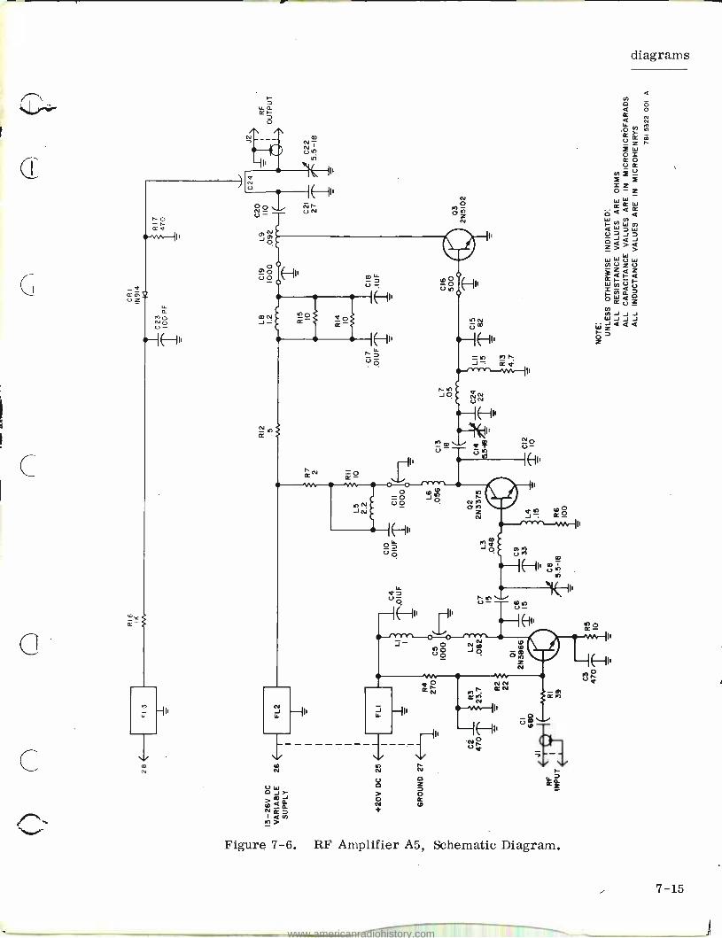
OpR NO L.)-
"2 1E-{,'
diagrams
Figure 7 -6. RF Amplifier A5, Schematic Diagram.
I
7 -15
www.americanradiohistory.com

diagrams
81 <
32 <
7 -16
100 UF ¢7 TPI + 8.24 oeG _.L )
CI R8 22 vF 10o IoK
41.0 UF NUM 267
24 1016
21 4.7ík G2
22 UF )
iL2 41K 14
R12
i.. 11:1 9 G
7 e10 100 SZ
11.1914 c22 Q IN914
211 1C,04
0o v sov
O I 21.12222 A
1 F PI-1 A.SE 214 C7 10 1-<00Ff.
215 lo
2.15 IOK
q2 = 21.129c11
TP3 RED
211
1270
2S
IS
TP4 2
- B528 100 Rp
Figure 7 -7. 785E -1 STL Interface Card A3, Schematic Diagram.
www.americanradiohistory.com

5 Io
;I-)
LLÑFO- 0
d Ó
a J
0 0 5
_J
En
thou J
ru S
c0
LL
LL O 0
u u 0
WJ
J
ú
www.americanradiohistory.com


dQ oá ttf
LL N M
Q
LL
O °
a Omó U- d8 Q
Za
LL?
Óñ dÁ
@@
J1 yi0
mú7j 3 Tá a d
jo ja
Q.3 "ai`v
d
a
,---, ° EL
g, H1'
nfi mó
r
PonEL d_ j}
> ed,-, aQ 1 7
d'I 4
s 0 o HI
NOEL
áä
90
rcdY
Ñ Ó il a d áá OYS ¿
'I(1 d I r I. VNQ i ÚQS nñ
.
n yy
H1. nr
Ú1 - w .n°4 mÑ Jl 90u ú°R 9O Ph
a
14 HI.
www.americanradiohistory.com


LL
u ¿ n° 0?
a
LLO n
rvP ttZ mm 7i
M +3r
LLQ ú
t ó ? öú ó$r rm+ na,q
rá "ÑW 11 O 0
d "-1 YVpll
d qg
$" ñ
N
o
o
www.americanradiohistory.com


r W1
41)
cIll 0 di
10 ro
d o 0?
4
(N
u
Mil ' m Ñ rzi
U N
K4 9 i +tY- 46- d O)
$u V 'S
Ñ a
roo ty
- CT)1 N
II) 9di
tun)
dl w
-LL U0)
{(
N
5
u
áó U0 9 H,ocóó
In a
7
r
2
J In In
IU
17
4 F J 0 >
U 4 >
r
U a >
N
{
- N (1) 4 N 9
et w
h 3 0 a
Ill
d
3Q ac
www.americanradiohistory.com


to 0
4 w 3 Ati
> d N 4
Qdi
da
N »
NN
r
Iio--
J á
dr 4 V
i $
Q N .1.
fi
e0
4
á
ti-
0 - -1
oü0
O.
á
R
á- a_ F0
F
0
www.americanradiohistory.com

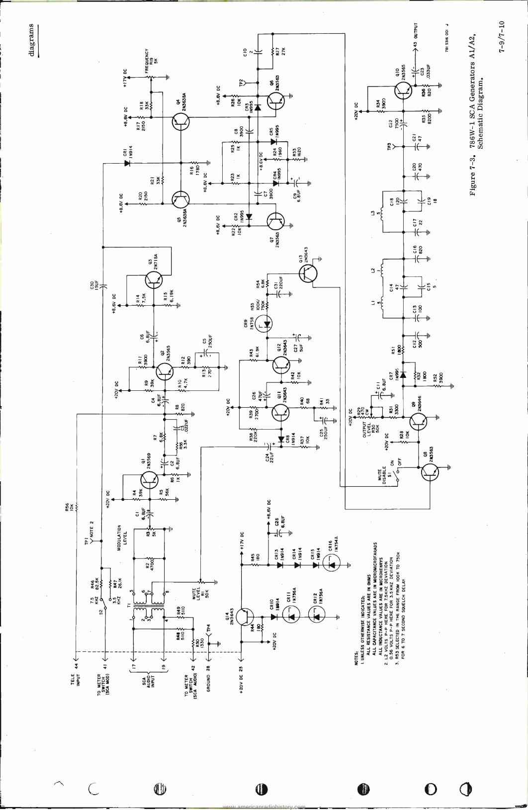
c
U
O.
c
o U
n IT
CC U Z
O Wru
n co o U Of U Z
C n
R r O
W J 7 w a h Z
ó
I-
á
p
v
-
J n
IE--jil
0 O W
1E-H0
v r Lc, Usr
TU 1n g U -
a 2 N
CO Y O
Ó + O
CO In CI
W z W N O O
VI O
Y W O p N 2 a > Z O r U i O p o
w
,21 5 2>> W
6 ' ° á N z z J z - z = Y O ó - w K < K n K1 =
W <nar cc (1.0 7 J N W Ncc O z W
O J< J ó W Cr (00
Z>>> K wIZ
r z vzcwi=a Z 2 z < z I - W O. & 6 ~ < a O N
á U a N Ñ r
N w 5
_ ~ OJ W
OF
- J Of J J J 0 y J 4-J
< Q N > n M z O
F- p _ R n li
O . z rn
www.americanradiohistory.com

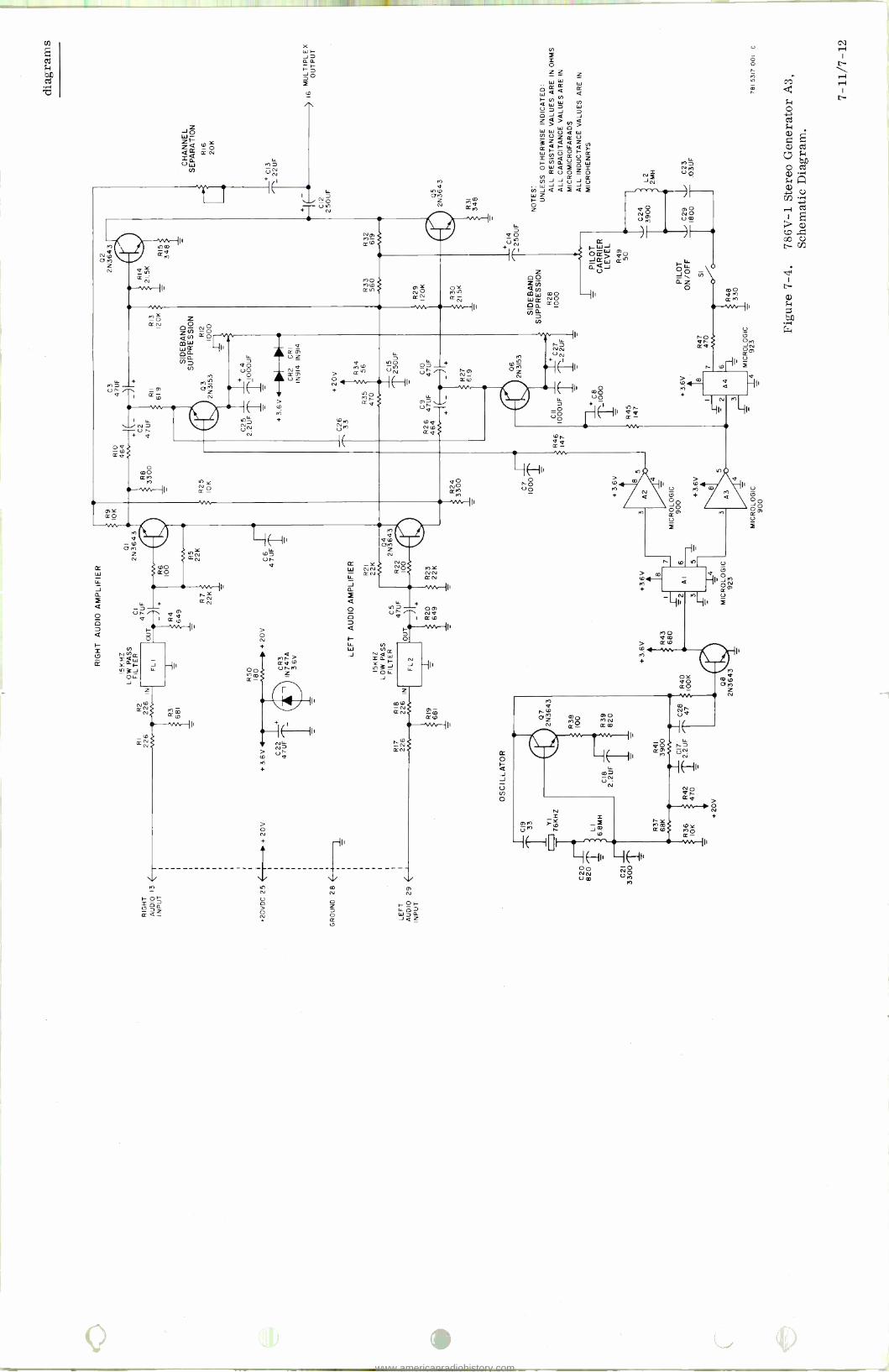
U O Cv
---v n,H I 1
O CO O 2 JO
I/)
II
X W 1- N JD f O . I ~ o
J p Z Z O - M K W
O a U yl a a a
n /\ a w 7 W U J O J a J
>> (n > o wwcWiaw N U z R U alaiaÿ w H Ú O~ K
~ N a U O W O w a E O 2
U O Z O
w J J U J U V 4 NU U) J a a f a f I
D 0 M W Z NU Z m FO
+T U N N N K Z 1
N
!Y
100 M ¢ u,
9II
LL O0 U
LL a N
+;VI
DO á(7) CD W W cr óa
a Cr)
I,- a, N J CCU)
vw,
U
7 O NO ¢m
HHI
+
Y
> O N +
_ Y N N K N
0 p N -
I I
DAL r N > U7 r N
+
O) N
O O
N
CO O N ¢ 0
HII o coo
+, EHII 7 -O
UO O
D N
N2 p
IOr JI V O
0
N R Q
rn
r cea
r1
(:J o) J N ¢
á N
--IHII
r0
m
M Q
ántO) m mo Z M 0 M N N a 2 CO
I1
-IHII ra U N
N _2 I mro > _f U M r J m
a,
H H
M
LL
P O r D CC 0) U N
N o vr cc vs.
r Y ro co
n Y cc (D O CC-
HII -IH. 00
N NO UM U(p
M
N +
Q U
www.americanradiohistory.com