3.3-ma 2.8-ghz bufferless lc oscillator directly driving a
TRANSCRIPT

LETTER
3.3-mA 2.8-GHz bufferless LC oscillator directly driving a 10-mmon-chip clock distribution line
Masahiro Ichihashi1a), Shogo Harada1, and Haruichi Kanaya1
Abstract A bufferless LC oscillator can potentially offer an attractivesolution for low-power, high-speed clock distribution due to the absenceof repeaters on the clock distribution line and utilization of LC resonance.However, conventional bufferless LC oscillators suffer from a fundamentaltradeoff between the frequency and power consumption due to their high-frequency sensitivity. In this paper, we have introduced a low-frequencysensitivity bufferless LC oscillator that is directly connected to a 10-mmon-chip clock distribution line in the TSMC 0.18-µm 1-Poly 6-MetalCMOS technology. The core area of the LC oscillator is only 270 × 280µm2. The measurement results show that a 2.8-GHz oscillation frequency,3.3-mA current consumption, and −112.8 dBc/Hz phase noise at 1MHzoffset can be achieved.Keywords: LC-oscillator, clock distribution, transmission lineClassification: Integrated circuits
1. Introduction
1.1 BackgroundHigh-speed clock distribution design has increasingly be-come important in determining the overall performance ofVLSI systems as it is associated with the highest power con-sumption. A large portion (40%–70%) of the total power canbe dissipated in microprocessors due to the high swing rateand large capacitance [1, 2, 3]. The effects of the number ofinverter-based repeaters on the clock distribution line withincreasing frequency and chip area in recent digital systemshave gained prominence due to the following reasons. First,a huge amount of power is dissipated due to the largevoltage swing level (usually 0 to Vdd). Second, a high-frequency operation is difficult owing to the high voltageswing level. Third, the Vdd sensitivity, known as the powersupply rejection ratio, is very high. A bufferless clock dis-tribution can offer an attractive solution to overcome theabove stated limitations. However, the fundamental tradeoffbetween the oscillation frequency and power consumption,as determined by Eq. (1) and (2), presents a practical prob-lem when such a bufferless structure is applied to a conven-tional LC oscillator. In Eq. (1) and (2), f, Ls, CD, Rs, and Rp
represent the oscillation frequency, series inductance, fre-quency tuning capacitance, series resistance, and equivalentparallel resistance, respectively as shown in Fig. 1.
f0 ¼ 1
2�ffiffiffiffiffiffiffiffiffiffiffiLsCD
p ð1Þ
I / 1
RpRp � !LsQ; Q ¼ !Ls
Rs
� �ð2Þ
1.2 Previous workMany works have been investigated for low-power resonantclock distribution [4, 5, 6, 7, 8, 9, 10, 11, 12, 13]. A 1.5-GHz bufferless LC oscillator introduced by Mesgarzadehet al. [4, 5] achieved an ∼57% lower clock power as com-pared to a conventional repeater-based LC oscillator. How-ever, this has not resolved the fundamental tradeoff betweenthe oscillation frequency and power consumption as thecircuit structure is based on the conventional LC oscillatorshown in Fig. 1. This makes operation at even higherfrequencies difficult due to the very small inductor value.
1.3 Objectives and scope of this studyWe have previously proposed a theory on the low-frequencysensitivity bufferless LC oscillators [6] to overcome thetradeoffs associated with conventional LC oscillators. Inthis paper, we present an experimental implementation ofthe previously proposed LC oscillator with the followingconditions. A differential signaling configuration in a 10-mm line is used for the clock distribution line as shown inFig. 2. Such a structure is commonly used in high-speedserial links that require the highest chip frequency [14, 15,16, 17]. However in this case, the 10-mm line has beenorganized to function as a meander line due to the limitedchip area. A length of 10mm allows the consideration ofhuge chips such as microprocessors [1]. The TSMC 0.18-µm 1-poly, 6-metal CMOS process was used for the fab-rication due to the limited options available in our labora-tory. A 2.8-GHz target frequency was selected as themaximum frequency in the worst case scenario at FO ¼ 4
(Fan Out) is ∼3-GHz for a 0.18-µm fabrication process.This measurement based approach not only establishes the
Fig. 1. A conventional LC oscillator.
DOI: 10.1587/elex.16.20190301Received May 12, 2019Accepted June 26, 2019Publicized July 31, 2019Copyedited August 25, 2019
1Dept. of Electronics, Graduate School of Information Scienceand Electrical Engineering, Kyushu University, Fukuoka 819–0395, Japana) [email protected]
IEICE Electronics Express, Vol.16, No.16, 1–5
1
Copyright © 2019 The Institute of Electronics, Information and Communication Engineers

low-frequency sensitivity feature but also shows the effectsof the transmission line on the LC oscillator. This paper isorganized as follows. A brief introduction on our proposedbufferless LC oscillator is described in Section 2, while thetest chip implementation is detailed in Section 3. Themeasurement results and analysis along with the mainconclusions are described in Sections 4 and 5, respectively.
2. Low-frequency sensitive bufferless LC oscillator
Fig. 3(a) and (b) show the conventional and proposed LC
oscillators [6], respectively. Fig. 3(b) indicates that the LC
tank is shared between the tuning capacitor CD and theloading of the clock distribution line CL by taking the tapfrom the inductor Lall at a certain point. Fig. 3(b) showsthat the impedance Zosc can be expressed by Eq. (3). Thesolution of Eq. (3) for a denominator equal to 0 is theoscillation frequency fp1. The output swing VOUT can beobtained using Eq. (2). Table I shows the theoretical differ-ence between the conventional and proposed LC oscilla-tors. Fig. 4(a) and (b) show the oscillation frequency fp1
and output swing VOUT . The figures clearly show that theproposed structure has a lower frequency and voltageswing sensitivity with an increase in the output loading CL
as compared to the conventional structure.
Zosc ¼ j!ðL1 þ L2 � !2L1L2CLÞ1 � !2L1CL � !2CDðL1 þ L2 � !2L1L2CLÞ ð3Þ
3. Test chip implementation
Fig. 5 and 6 show the structure of the fabricated circuit andphotograph of the chip. The circuit has an 8-shaped differ-ential inductor [18, 19, 20, 21, 22, 23, 24] with L ¼ 2:86nHand �TAP ¼ 0:5. The LC oscillator has a core area of only270 � 280µm2. The 10-mm on-chip clock distribution lineis organized by the meander line using a thick metal layer(M6), and width and space of 2 µm each taking into con-sideration the limited chip area and resistive loss. Thedifferential signal obtained after clock distribution is buf-
fered using a 5-stage FO ¼ 2 current-mode logic and finallyoutput with an impedance of 50Ω to the PAD for thepurposes of measurement.
4. Measurement results and analysis
4.1 Measurement setupThe measurements from the proposed bufferless LC oscil-
Fig. 2. A differential signaling configuration for high-speed serial links.
(a) Conventional (b) Proposed
Fig. 3. The conventional and proposed [6] LC oscillators.
Table I. A comparison between the conventional and proposed LC
oscillators.
Param. Conventional Proposed
fp1 �p1 � f0 �p1 � f0
f0
1
2�ffiffiffiffiffiffiffiffiffiffiffiffiffiLallCD
p 1
2�ffiffiffiffiffiffiffiffiffiffiffiffiffiLallCD
p
�p11ffiffiffiffiffiffiffiffiffiffiffiffiffiffiffiffiffiffiffiffiffiffi
1 þ CL=CD
p 1ffiffiffiffiffiffiffiffiffiffiffiffiffiffiffiffiffiffiffiffiffiffiffiffiffiffiffiffiffiffiffiffiffiffi1 þ �TAP � CL=CD
p
Qall2�fp1Lall
Rall
2�fp1fLall � CLð�TAPRallÞ2gRall
Rp:all Qall2 � Rall Qall
2 � Rall
VOUT4
�� I � Rp:all
4
�� I � Rp:all � �TAP
Here,Lall ¼ L1 þ L2 L1 ¼ �TAP � LallRall : parasitic resistance of Lall �CL ¼ 0
(a) Oscillation frequency fp1 vs CL
(b) Voltage swing VOUT vs CLΔ
Δ
Fig. 4. Sensitivity of the oscillation frequency and voltage swing.
IEICE Electronics Express, Vol.16, No.16, 1–5
2
lator are recorded using a 50Ω probe station and signalsource analyzer via semi-rigid cables. The GSGSG probeemployed has an open-circuit input capacitance of 5.4 fF.Thus, the gain-loss for this measurement setup is mainlyfrom the cable-loss and is 2.6 dB at 3GHz. It should benoted that the phase noise is measured after LNA (39.5 dB)to amplify the output signal as the output level was not ashigh as expected. This problem will be further discussed inSection 4.3.
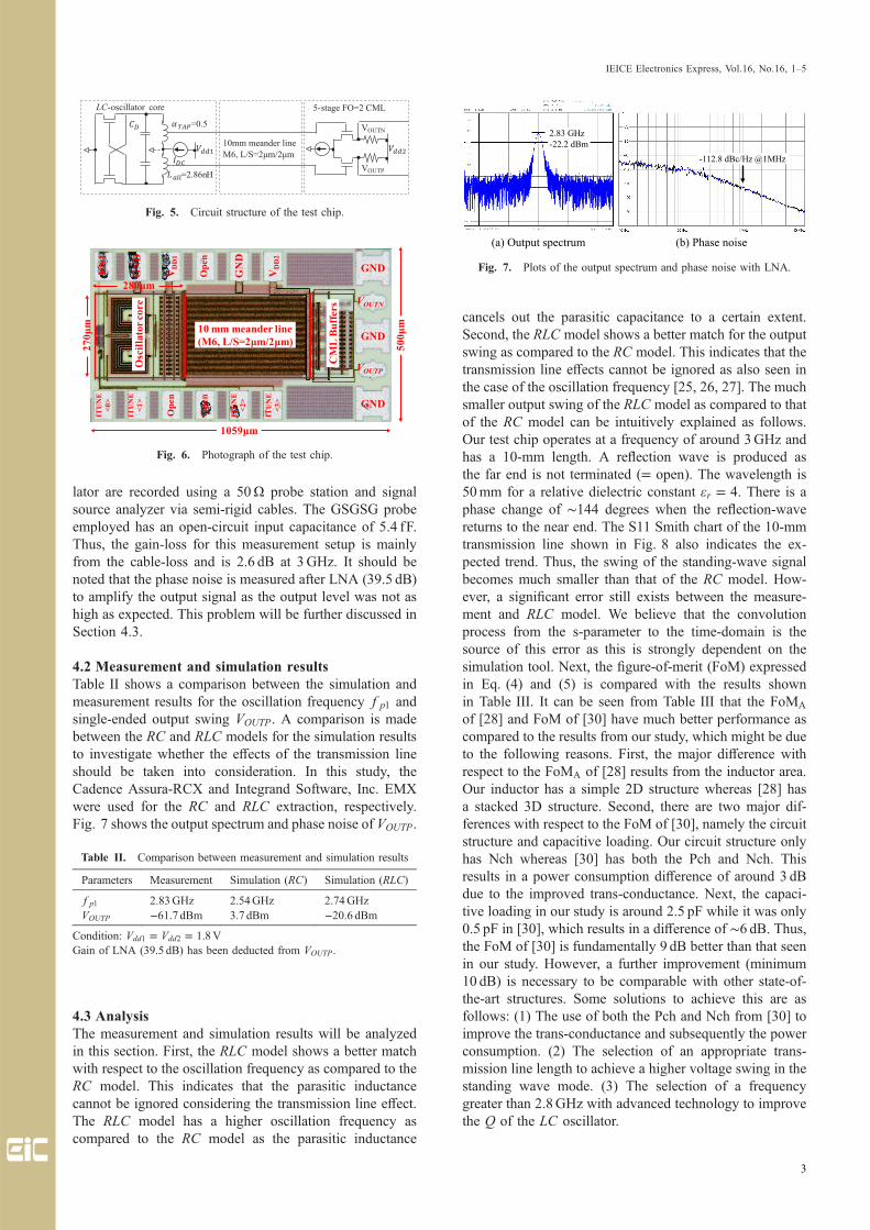
4.2 Measurement and simulation resultsTable II shows a comparison between the simulation andmeasurement results for the oscillation frequency fp1 andsingle-ended output swing VOUTP. A comparison is madebetween the RC and RLC models for the simulation resultsto investigate whether the effects of the transmission lineshould be taken into consideration. In this study, theCadence Assura-RCX and Integrand Software, Inc. EMXwere used for the RC and RLC extraction, respectively.Fig. 7 shows the output spectrum and phase noise of VOUTP.
4.3 AnalysisThe measurement and simulation results will be analyzedin this section. First, the RLC model shows a better matchwith respect to the oscillation frequency as compared to theRC model. This indicates that the parasitic inductancecannot be ignored considering the transmission line effect.The RLC model has a higher oscillation frequency ascompared to the RC model as the parasitic inductance
cancels out the parasitic capacitance to a certain extent.Second, the RLC model shows a better match for the outputswing as compared to the RC model. This indicates that thetransmission line effects cannot be ignored as also seen inthe case of the oscillation frequency [25, 26, 27]. The muchsmaller output swing of the RLC model as compared to thatof the RC model can be intuitively explained as follows.Our test chip operates at a frequency of around 3GHz andhas a 10-mm length. A reflection wave is produced asthe far end is not terminated (= open). The wavelength is50mm for a relative dielectric constant "r ¼ 4. There is aphase change of ∼144 degrees when the reflection-wavereturns to the near end. The S11 Smith chart of the 10-mmtransmission line shown in Fig. 8 also indicates the ex-pected trend. Thus, the swing of the standing-wave signalbecomes much smaller than that of the RC model. How-ever, a significant error still exists between the measure-ment and RLC model. We believe that the convolutionprocess from the s-parameter to the time-domain is thesource of this error as this is strongly dependent on thesimulation tool. Next, the figure-of-merit (FoM) expressedin Eq. (4) and (5) is compared with the results shownin Table III. It can be seen from Table III that the FoMA
of [28] and FoM of [30] have much better performance ascompared to the results from our study, which might be dueto the following reasons. First, the major difference withrespect to the FoMA of [28] results from the inductor area.Our inductor has a simple 2D structure whereas [28] hasa stacked 3D structure. Second, there are two major dif-ferences with respect to the FoM of [30], namely the circuitstructure and capacitive loading. Our circuit structure onlyhas Nch whereas [30] has both the Pch and Nch. Thisresults in a power consumption difference of around 3 dBdue to the improved trans-conductance. Next, the capaci-tive loading in our study is around 2.5 pF while it was only0.5 pF in [30], which results in a difference of ∼6 dB. Thus,the FoM of [30] is fundamentally 9 dB better than that seenin our study. However, a further improvement (minimum10 dB) is necessary to be comparable with other state-of-the-art structures. Some solutions to achieve this are asfollows: (1) The use of both the Pch and Nch from [30] toimprove the trans-conductance and subsequently the powerconsumption. (2) The selection of an appropriate trans-mission line length to achieve a higher voltage swing in thestanding wave mode. (3) The selection of a frequencygreater than 2.8GHz with advanced technology to improvethe Q of the LC oscillator.
Fig. 6. Photograph of the test chip.
Table II. Comparison between measurement and simulation results
Parameters Measurement Simulation (RC) Simulation (RLC)
fp1 2.83GHz 2.54GHz 2.74GHzVOUTP −61.7 dBm 3.7 dBm −20.6 dBm
Condition: Vdd1 ¼ Vdd2 ¼ 1:8VGain of LNA (39.5 dB) has been deducted from VOUTP.
(a) Output spectrum (b) Phase noise
Fig. 7. Plots of the output spectrum and phase noise with LNA.
Fig. 5. Circuit structure of the test chip.
IEICE Electronics Express, Vol.16, No.16, 1–5
3

FoM ¼ Lð�fÞ � 20logf0
�f
� �þ 10log
Pdc
1mW
� �ð4Þ
FoMA ¼ FoM þ 10logArea
1mm2
� �ð5Þ
Here,f0 : oscillation frequency �f : offset frequencyPdc : power consumption Lð�fÞ : phase noise at �f
5. Conclusion
In this paper, we introduced a low-frequency sensitivitybufferless LC oscillator that is directly connected to a 10-mm on-chip clock distribution line. The low-frequencysensitivity feature enables high-speed operation even inthe case of heavy capacitive loading. In addition, it wasalso found that the standing wave mode is generated whenthe long transmission line is directly connected. A low-power, high-frequency system can be realized by selectingan appropriate transmission line length and frequency. Thetest chip has been fabricated using the TSMC 1-poly, 6-metal CMOS technology with an oscillator core area ofonly 270 � 280µm2. The measurement results demonstratethat a 2.83-GHz frequency, 3.3-mA current consumption,and −112.8 dBc/Hz phase noise at 1-MHz offset can beachieved.
Acknowledgments
This work was partially supported by the Grant-in-Aid forScientific Research (KAKENHI, 18K04146) from the Ja-pan Society for the Promotion of Science (JSPS), VLSIDesign and Education Center (VDEC), Integrand Software,Inc. and the Grant-in-Aid for the Collaborative ResearchProgram Based on Industrial Demand, CREST(JPMJCR1431) and the Matching planner program fromthe Japan Science and Technology Agency, JST and NEDO(New Energy and Industrial Technology DevelopmentOrganization), and SIP (Cross-ministerial Strategic Innova-tion Promotion Program). We would like to thank Editage(www.editage.jp) for English language editing.
References
[1] P. J. Restle, et al.: “A clock distribution network for micro-processors,” IEEE J. Solid-State Circuits 36 (2001) 792 (DOI:10.1109/4.918917).
[2] P. E. Gronowski, et al.: “High-performance microprocessordesign,” IEEE J. Solid-State Circuits 33 (1998) 676 (DOI:10.1109/4.668981).
[3] A. J. Drake, et al.: “Resonant clocking using distributed parasiticcapacitance,” IEEE J. Solid-State Circuits 39 (2004) 1520 (DOI:10.1109/JSSC.2004.831435).
[4] B. Mesgarzadeh, et al.: “Low-power bufferless resonant clockdistribution networks,” Circuits and Systems, 2007. MWSCAS2007 (2007) (DOI: 10.1109/MWSCAS.2007.4488725).
[5] B. Mesgarzadeh, et al.: “Jitter characteristic in charge recoveryresonant clock distribution,” IEEE J. Solid-State Circuits 42 (2007)1618 (DOI: 10.1109/JSSC.2007.896691).
[6] M. Ichihashi and H. Kanaya: “A low-power and GHz-band LC-DCO directly drives 10mm on-chip clock distribution line in 0.18µm CMOS,” IEICE Trans. Fundamentals E101-A (2018) 1907(DOI: 10.1587/transfun.E101.A.1907).
[7] F. O’Mahony, et al.: “A low-jitter PLL and repeaterless clockdistribution network for a 20Gb/s link,” 2006 Symposium onVLSI Circuits Digest of Technical Papers (2006) (DOI: 10.1109/VLSIC.2006.1705296).
[8] Y. Xu, et al.: “Bufferless resonant clocking with low skew and highvariation-tolerant,” Circuits and Systems (MWSCAS) (2011) (DOI:10.1109/MWSCAS.2011.6026650).
[9] Y. Xu and S.-M. Chen: “Research of transformer based bufferlessresonant clock network,” Solid-State and Integrated CircuitTechnology (ICSICT) (2010) (DOI: 10.1109/ICSICT.2010.5667716).
[10] F. O’Mahony, et al.: “A 10-GHz global clock distribution usingcoupled standing-wave oscillators,” IEEE J. Solid-State Circuits 38(2003) 1813 (DOI: 10.1109/JSSC.2003.818299).
[11] S. Chan, et al.: “A resonant global clock distribution for the cellbroadband engine processor,” Solid-State Circuits Conference,2008. ISSCC 2008. Digest of Technical Papers. IEEE International(2008) (DOI: 10.1109/ISSCC.2008.4523282).
[12] M. R. Guthaus and B. Taskin: “High-performance, low-powerresonant clocking,” Computer-Aided Design (ICCAD) (2012).
[13] P.-Y. Lin, et al.: “LC resonant clock resource minimization usingcompensation capacitance,” Circuits and Systems (ISCAS) (2015)(DOI: 10.1109/ISCAS.2015.7168906).
[14] J. Poulton, et al.: “A 14-mW 6.25-Gb/s transceiver in 90-nmCMOS,” IEEE J. Solid-State Circuits 42 (2007) 2745 (DOI: 10.1109/JSSC.2007.908692).
[15] K. Fukuda, et al.: “A 12.3-mW 12.5-Gb/s complete transceiver in65-nm CMOS process,” IEEE J. Solid-State Circuits 45 (2010)2838 (DOI: 10.1109/JSSC.2010.2075410).
[16] T. Shibasaki, et al.: “18-GHz clock distribution using a coupledVCO array,” IEICE Trans. Electron. E90-C (2007) 811 (DOI: 10.1093/ietele/e90-c.4.811).
[17] K. Hu, et al.: “Comparison of on-die global clock distribution
Table III. Comparison results for the FoM and FoMA from variousstudies.
[28] [29] [30] [31]Thiswork
Tech[nm]
65 180 130 55 180
Area[µm2]
484 1260460 695520 597600 75600
Lð�fÞ[dBc/Hz]
−110 −116 −120.6 −100.5 −112.8
f0
[GHz]21 5.32 5.29 80 2.83
�f
[MHz]10 1 1 1 1
Pdc
[mW]1.92 5.71 1.98 18 5.94
FoM[dBc/Hz]
−173.6 −183.0 −192.1 −186.0 −174.1
FoMA
[dBc/Hz]−206.8 −181.9 −193.7 −188.2 −185.3
Fig. 8. The S11 smith chart of the 10-mm transmission line (input:50Ω, output: open).
IEICE Electronics Express, Vol.16, No.16, 1–5
4

methods for parallel serial links,” Circuits and Systems, 2009.ISCAS (2009) (DOI: 10.1109/ISCAS.2009.5118137).
[18] M. Ichihashi and H. Kanaya: “A high-frequency, low-coupling 8-shaped differential inductor with patterned ground shield,”Microw.Opt. Technol. Lett. 60 (2018) 2704 (DOI: 10.1002/mop.31469).
[19] P. Findley, et al.: “Novel differential inductor design for high self-resonance frequency,” Electron Devices Meeting, 2004. IEDMTechnical Digest. IEEE International. IEEE (2004) (DOI: 10.1109/IEDM.2004.1419189).
[20] C. P. Yue and S. S. Wong: “On-chip spiral inductors with patternedground shields for Si-based RF IC’s,” VLSI Circuits. 1997. Digestof Technical Papers (1997) (DOI: 10.1109/VLSIC.1997.623819).
[21] S.-M. Yim: “The effects of a ground shield on the characteristicsand performance of spiral inductors,” IEEE J. Solid-State Circuits37 (2002) 237 (DOI: 10.1109/4.982430).
[22] X. Xu, et al.: “Design of novel high-Q-factor multipath stackedon-chip spiral inductors,” IEEE Trans. Electron Devices 59 (2012)2011 (DOI: 10.1109/TED.2012.2197626).
[23] P.-Y. Wang, et al.: “A low phase-noise class-C VCO using novel 8-shaped transformer,” Circuits and Systems (ISCAS) IEEE Interna-tional Symposium (2015) (DOI: 10.1109/ISCAS.2015.7168776).
[24] N. M. Neihart, et al.: “Twisted inductors for low coupling mixed-signal and RF applications,” Custom Integrated Circuits Confer-ence (2008) (DOI: 10.1109/CICC.2008.4672150).
[25] K. Banerjee and A. Mehrotra: “Analysis of on-chip inductanceeffects for distributed RLC interconnects,” IEEE Transactions onComputer-Aided Design of Integrated Circuits and Systems, Proc.of the 38th Design Automation Conference (2001) 798 (DOI:10.1145/378239.379069).
[26] M. A. El-Moursy and E. G. Friedman: “Power characteristics ofinductive interconnect,” IEEE Trans. Very Large Scale Integr.(VLSI) Syst. 12 (2004) 1295 (DOI: 10.1109/TVLSI.2004.834227).
[27] P. Heydari, et al.: “A comprehensive study of energy dissipation inlossy transmission lines driven by CMOS inverters,” Proc. of theIEEE 2002 Custom Integrated Circuits Conference (2002) 517(DOI: 10.1109/CICC.2002.1012895).
[28] R. Murakami, et al.: “A 484- m2 21-GHz LC-VCO beneath astacked-spiral inductor,” Microwave Conference (EuMC) (2010).
[29] Y. Shin, et al.: “A low phase noise fully integrated CMOS LCVCO using a large gate length pMOS current source and biasfiltering technique for 5-GHz WLAN,” Signals, Systems andElectronics (2007) (DOI: 10.1109/ISSSE.2007.4294527).
[30] A. El Oualkadi: “5-GHz low phase noise CMOS LC-VCO withPGS inductor suitable for ultra-low power applications,” Micro-wave Symposium (MMS) (2009) (DOI: 10.1109/MMS.2009.5409799).
[31] L. Iotti, et al.: “Insights into phase-noise scaling in switch-coupledmulti-core LC VCOs for E-band adaptive modulation links,” IEEEJ. Solid-State Circuits 52 (2017) 1703 (DOI: 10.1109/JSSC.2017.2697442).
IEICE Electronics Express, Vol.16, No.16, 1–5
5