361 multipath..1 ece 361 computer architecture lecture 10: designing a multiple cycle processor
Post on 20-Dec-2015
223 views
TRANSCRIPT

361 multipath..1
ECE 361Computer Architecture
Lecture 10: Designing a Multiple Cycle Processor
361 multipath..2
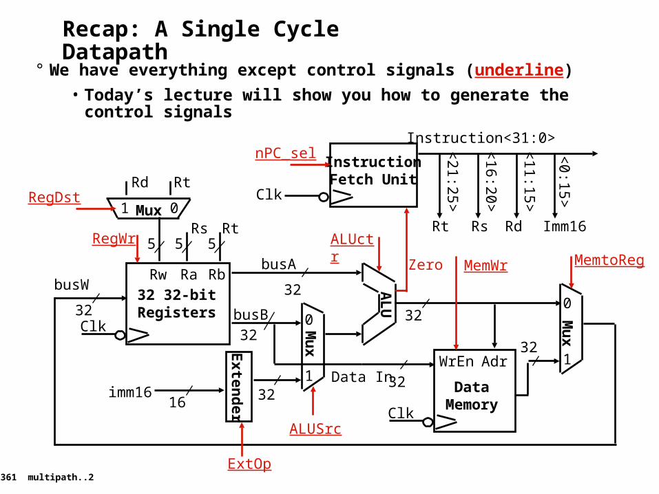
Recap: A Single Cycle Datapath
° We have everything except control signals (underline)
• Today’s lecture will show you how to generate the control signals
32
ALUctr
Clk
busW
RegWr
32
32
busA
32
busB
55 5
Rw Ra Rb
32 32-bitRegisters
Rs
Rt
Rt
RdRegDst
Exten
der
Mu
x
Mux
3216imm16
ALUSrc
ExtOp
Mu
x
MemtoReg
Clk
Data InWrEn
32
Adr
DataMemory
32
MemWrA
LU
InstructionFetch Unit
Clk
Zero
Instruction<31:0>
0
1
0
1
01<
21:25>
<16:20>
<11:15>
<0:15>
Imm16RdRsRt
nPC_sel

361 multipath..3
Recap: PLA Implementation of the Main Control
op<0>
op<5>. .op<5>. .<0>
op<5>. .<0>
op<5>. .<0>
op<5>. .<0>
op<5>. .<0>
R-type ori lw sw beq jumpRegWrite
ALUSrc
MemtoReg
MemWrite
Branch
Jump
RegDst
ExtOp
ALUop<2>
ALUop<1>
ALUop<0>
361 multipath..4
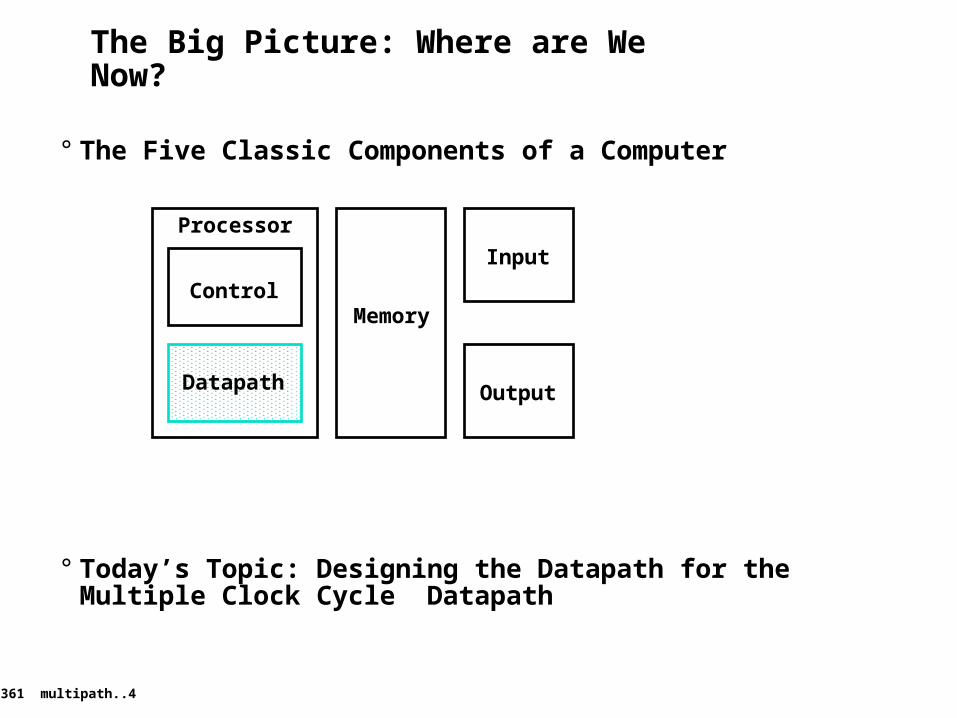
The Big Picture: Where are We Now?
° The Five Classic Components of a Computer
° Today’s Topic: Designing the Datapath for the Multiple Clock Cycle Datapath
Control
Datapath
Memory
Processor
Input
Output
361 multipath..5
Outline of Today’s Lecture
° Recap and Introduction
° Introduction to the Concept of Multiple Cycle Processor
° Multiple Cycle Implementation of R-type Instructions
° What is a Multiple Cycle Delay Path and Why is it Bad?
° Multiple Cycle Implementation of Or Immediate
° Multiple Cycle Implementation of Load and Store
° Putting it all Together
361 multipath..6
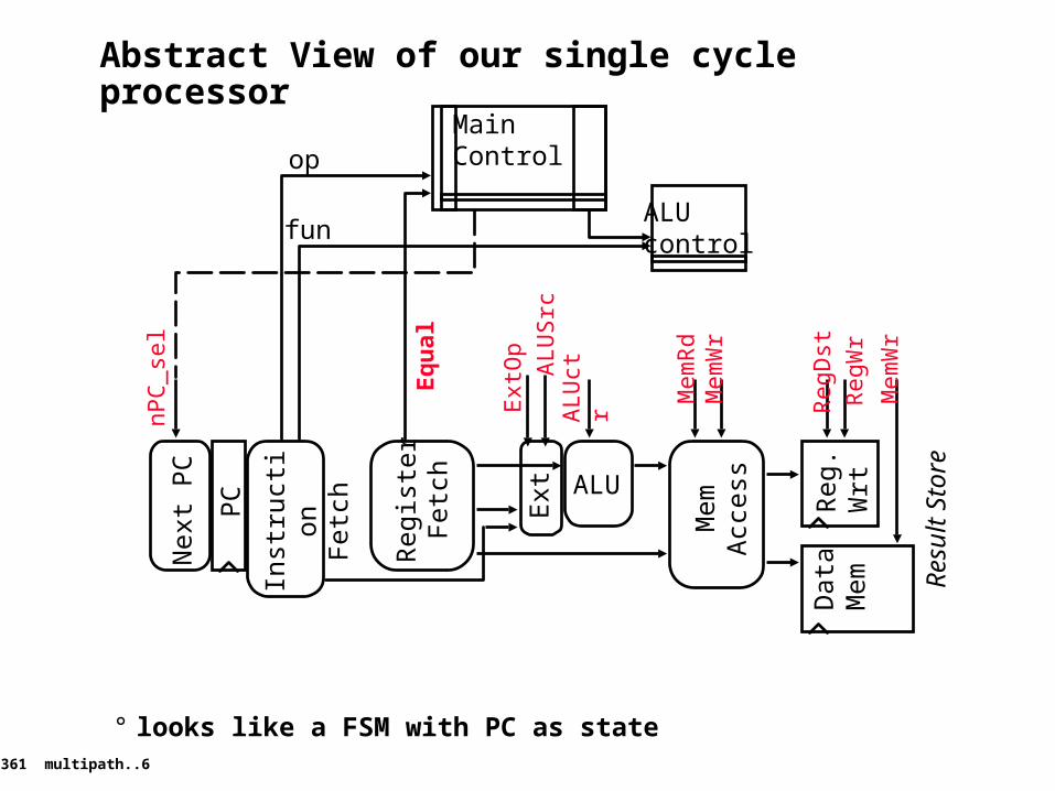
Abstract View of our single cycle processor
° looks like a FSM with PC as state
PC
Nex
t P
C
Reg
iste
rF
etch ALU Reg
. W
rt
Mem
Acc
ess
Dat
aM
emInst
ruct
ion
Fet
ch
Res
ult
Sto
re
AL
Uct
r
Reg
Dst
AL
US
rc
Ext
Op
Mem
Wr
Eq
ual
nPC
_sel
Reg
Wr
Mem
Wr
Mem
Rd
MainControl
ALUcontrol
op
fun
Ext
361 multipath..7
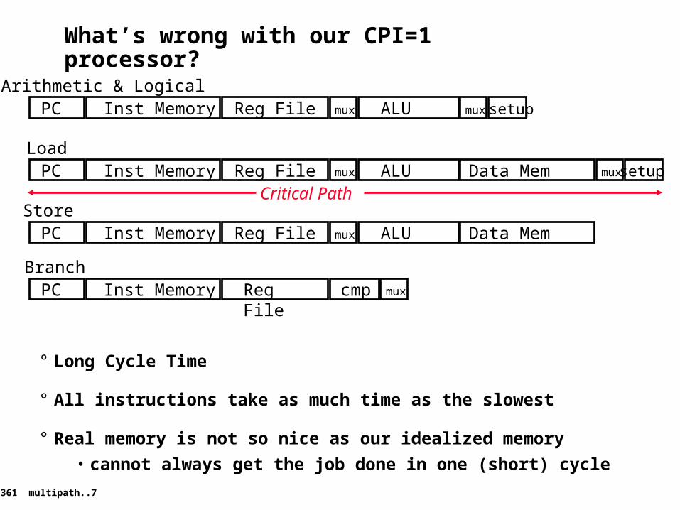
What’s wrong with our CPI=1 processor?
° Long Cycle Time
° All instructions take as much time as the slowest
° Real memory is not so nice as our idealized memory
• cannot always get the job done in one (short) cycle
PC Inst Memory mux ALU Data Mem mux
PC Reg FileInst Memory mux ALU mux
PC Inst Memory mux ALU Data Mem
PC Inst Memory cmp mux
Reg File
Reg File
Reg File
Arithmetic & Logical
Load
Store
Branch
Critical Path
setup
setup

361 multipath..8
Drawbacks of this Single Cycle Processor
° Long cycle time:
• Cycle time must be long enough for the load instruction:
- PC’s Clock -to-Q +
- Instruction Memory Access Time +
- Register File Access Time +
- ALU Delay (address calculation) +
- Data Memory Access Time +
- Register File Setup Time +
- Clock Skew
° Cycle time is much longer than needed for all other instructions. Examples:
• R-type instructions do not require data memory access
• Jump does not require ALU operation nor data memory access
361 multipath..9
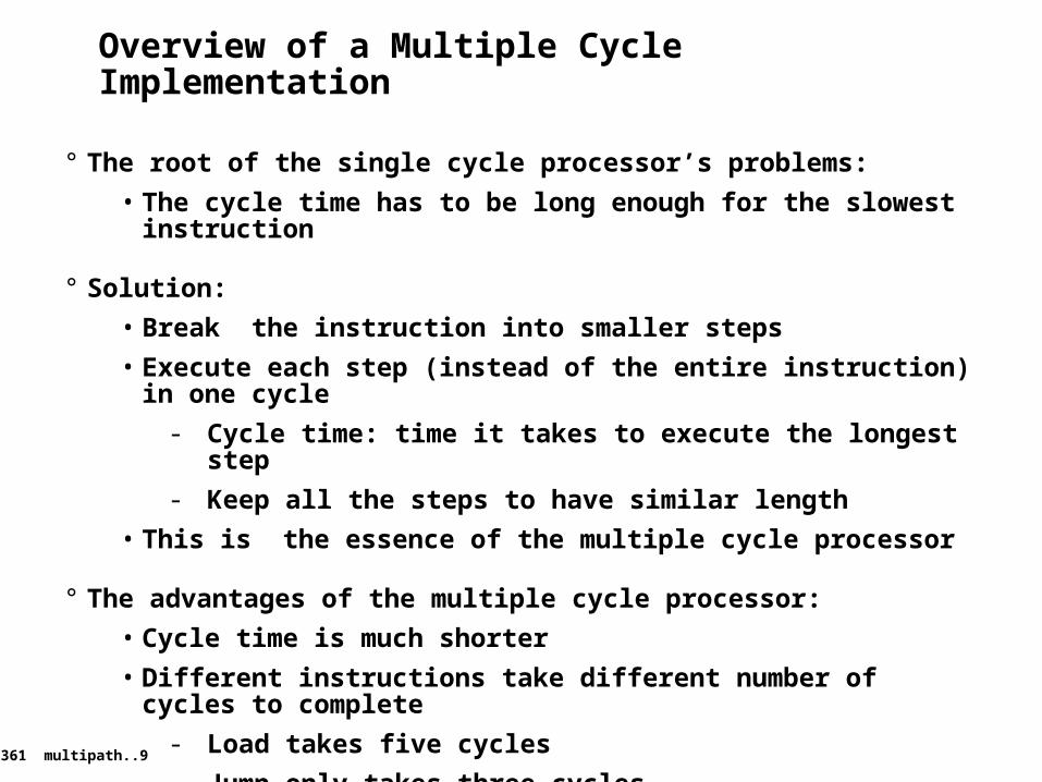
Overview of a Multiple Cycle Implementation
° The root of the single cycle processor’s problems:
• The cycle time has to be long enough for the slowest instruction
° Solution:
• Break the instruction into smaller steps
• Execute each step (instead of the entire instruction) in one cycle
- Cycle time: time it takes to execute the longest step
- Keep all the steps to have similar length
• This is the essence of the multiple cycle processor
° The advantages of the multiple cycle processor:
• Cycle time is much shorter
• Different instructions take different number of cycles to complete
- Load takes five cycles
- Jump only takes three cycles
• Allows a functional unit to be used more than once per instruction

361 multipath..10
The Five Steps of a Load Instruction
Clk
PC
Rs, Rt, Rd,Op, Func
Clk-to-Q
ALUctr
Instruction Memory Access Time
Old Value New Value
RegWr Old Value New Value
Delay through Control Logic
busARegister File Access Time
Old Value New Value
busB
ALU Delay
Old Value New Value
Old Value New Value
New ValueOld Value
ExtOp Old Value New Value
ALUSrc Old Value New Value
Address Old Value New Value
busW Old Value New
Delay through Extender & Mux
Data Memory Access Time
Instruction Fetch Instr Decode /
Reg. Fetch
Address Reg WrData Memory
Register F
ile Write T
ime
361 multipath..11
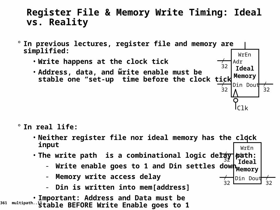
Register File & Memory Write Timing: Ideal vs. Reality
° In previous lectures, register file and memory are simplified:
• Write happens at the clock tick
• Address, data, and write enable must bestable one “set-up” time before the clock tick
° In real life:
• Neither register file nor ideal memory has the clock input
• The write path is a combinational logic delay path:
- Write enable goes to 1 and Din settles down
- Memory write access delay
- Din is written into mem[address]
• Important: Address and Data must bestable BEFORE Write Enable goes to 1
Adr
Din
WrEn
Dout
IdealMemory
32
32 32
Clk
Adr
Din
WrEn
Dout
IdealMemory
32
32 32
361 multipath..12
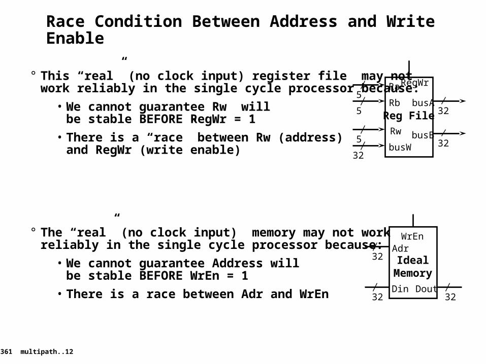
Race Condition Between Address and Write Enable
° This “real” (no clock input) register file may notwork reliably in the single cycle processor because:
• We cannot guarantee Rw willbe stable BEFORE RegWr = 1
• There is a “race” between Rw (address)and RegWr (write enable)
° The “real” (no clock input) memory may not workreliably in the single cycle processor because:
• We cannot guarantee Address willbe stable BEFORE WrEn = 1
• There is a race between Adr and WrEn
Reg File
Ra
Rw
busW
Rb busA
busB
RegWr5
5
5
3232
32
Adr
Din
WrEn
Dout
IdealMemory
32
32 32
361 multipath..13
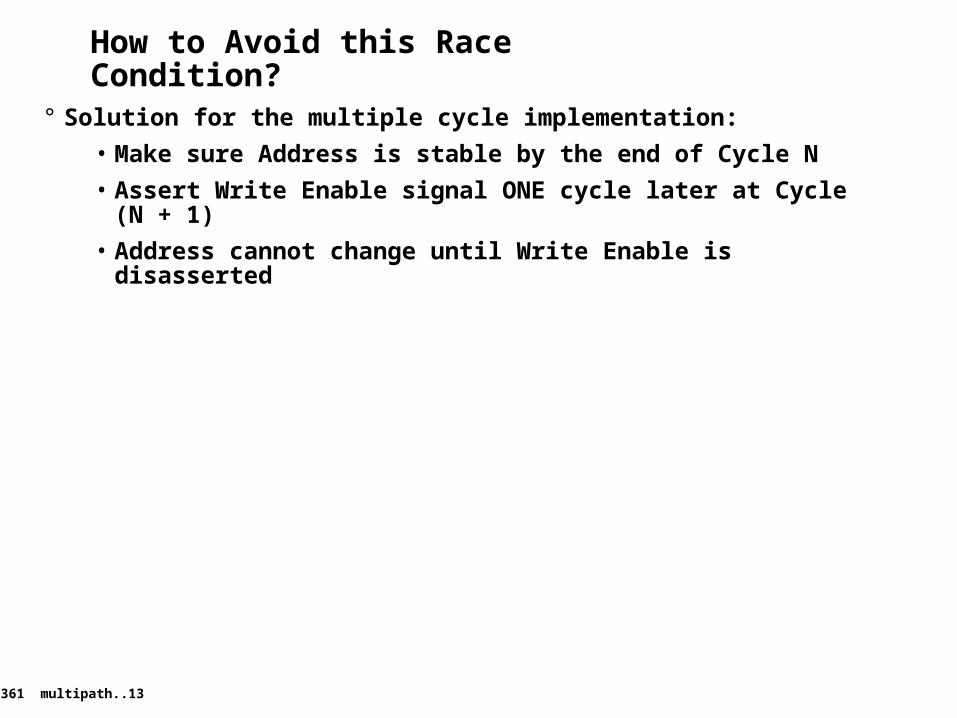
How to Avoid this Race Condition?
° Solution for the multiple cycle implementation:
• Make sure Address is stable by the end of Cycle N
• Assert Write Enable signal ONE cycle later at Cycle (N + 1)
• Address cannot change until Write Enable is disasserted
361 multipath..14
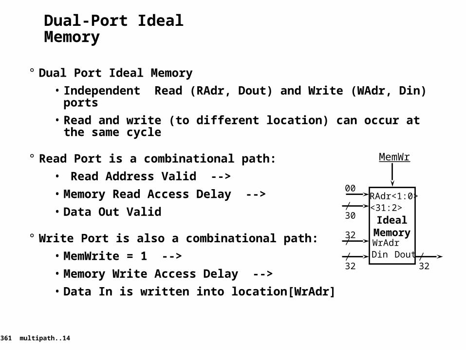
Dual-Port Ideal Memory
° Dual Port Ideal Memory
• Independent Read (RAdr, Dout) and Write (WAdr, Din) ports
• Read and write (to different location) can occur at the same cycle
° Read Port is a combinational path:
• Read Address Valid -->
• Memory Read Access Delay -->
• Data Out Valid
° Write Port is also a combinational path:
• MemWrite = 1 -->
• Memory Write Access Delay -->
• Data In is written into location[WrAdr]
IdealMemory
<31:2>
WrAdrDin
RAdr<1:0>00
30
32
32 32Dout
MemWr
361 multipath..16
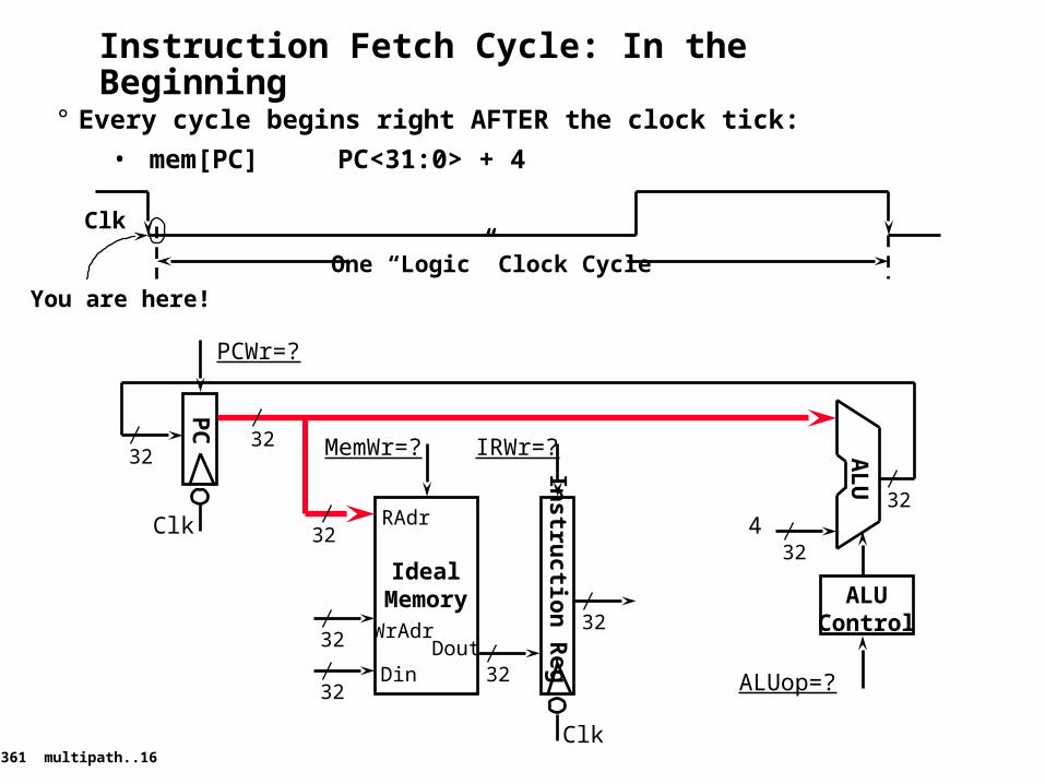
Instruction Fetch Cycle: In the Beginning
° Every cycle begins right AFTER the clock tick:
• mem[PC] PC<31:0> + 4
IdealMemory
WrAdr
Din
RAdr32
32
3232
Dout
MemWr=?
PC
3232
Clk
AL
U
32
32
ALUop=?
ALUControl
4
Instru
ction R
eg
32
IRWr=?
Clk
PCWr=?
Clk
You are here!
One “Logic” Clock Cycle
361 multipath..17
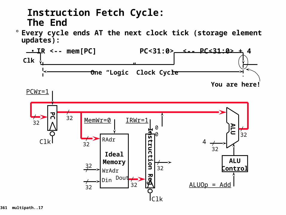
Instruction Fetch Cycle: The End
° Every cycle ends AT the next clock tick (storage element updates):
• IR <-- mem[PC] PC<31:0> <-- PC<31:0> + 4
IdealMemoryWrAdr
Din
RAdr32
32
32 32Dout
MemWr=0
PC
3232
Clk
AL
U
32
32
ALUOp = Add
ALUControl
4
00In
struction
Reg
32
IRWr=1
Clk
PCWr=1
Clk
You are here!
One “Logic” Clock Cycle
361 multipath..18
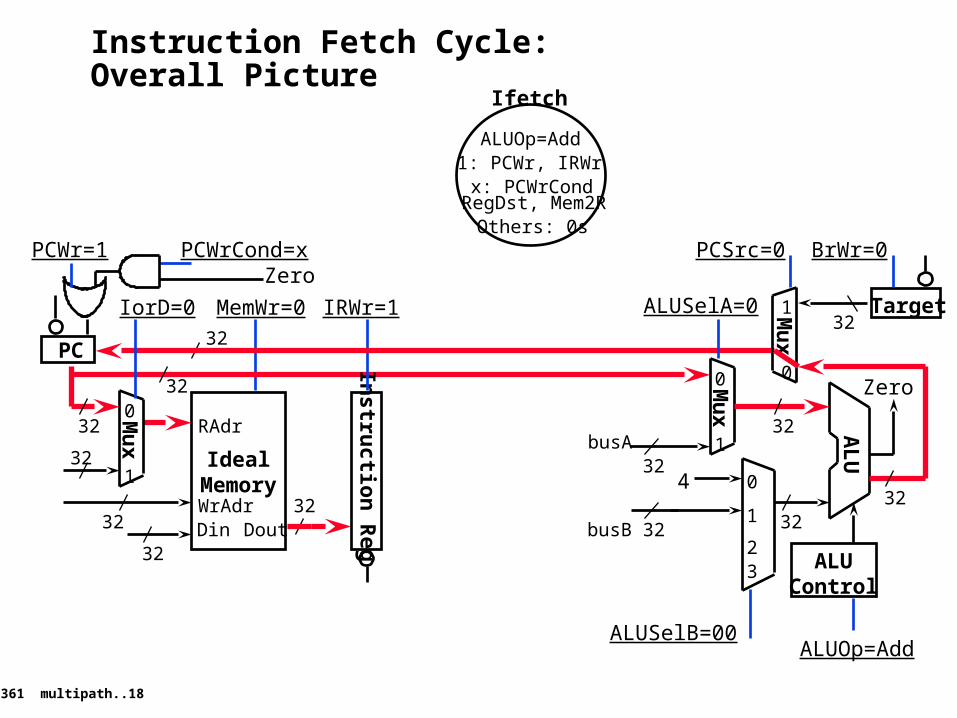
Instruction Fetch Cycle: Overall Picture
Target
IdealMemoryWrAdrDin
RAdr
32
32
32Dout
MemWr=0
32
AL
U
3232
ALUOp=Add
ALUControl
Instru
ction R
eg
IRWr=1
32
32busA
32busB
PCWr=1
ALUSelA=0
Mu
x
0
1
32
PC
Mu
x
0
132
0
1
23
4
ALUSelB=00
Mu
x
1
0
32
Zero
ZeroPCWrCond=x PCSrc=0 BrWr=0
32
IorD=0
1: PCWr, IRWrALUOp=Add
Others: 0s
x: PCWrCondRegDst, Mem2R
Ifetch
361 multipath..19
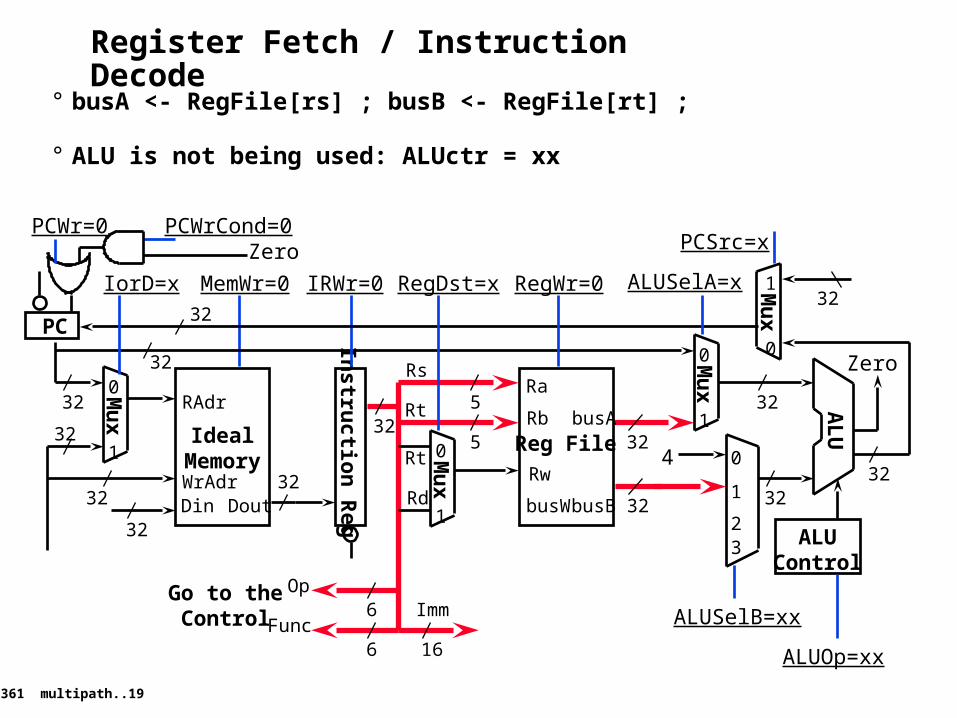
Register Fetch / Instruction Decode
° busA <- RegFile[rs] ; busB <- RegFile[rt] ;
° ALU is not being used: ALUctr = xx
IdealMemoryWrAdrDin
RAdr
32
32
32Dout
MemWr=0
32
AL
U
3232
ALUOp=xx
ALUControl
Instru
ction R
eg
32
IRWr=0
32
Reg File
Ra
Rw
busW
Rb5
5
32busA
32busB
RegWr=0
Rs
Rt
Mu
x
0
1
Rt
Rd
PCWr=0
ALUSelA=xRegDst=x
Mu
x
0
1
32
PC
Mu
x
0
132
0
1
23
4
16
Imm ALUSelB=xx
Mu
x
1
0
32
Zero
ZeroPCWrCond=0
PCSrc=x
32
IorD=x
Func
OpGo to theControl 6
6
361 multipath..20
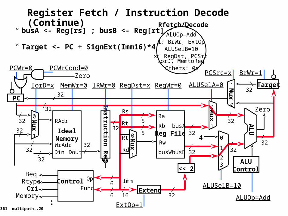
Register Fetch / Instruction Decode (Continue)
° busA <- Reg[rs] ; busB <- Reg[rt] ;
° Target <- PC + SignExt(Imm16)*4
Target
IdealMemoryWrAdrDin
RAdr
32
32
32Dout
MemWr=0
32
AL
U
3232
ALUOp=Add
ALUControl
Instru
ction R
eg
32
IRWr=0
32
Reg File
Ra
Rw
busW
Rb5
5
32busA
32busB
RegWr=0
Rs
Rt
Mu
x
0
1
Rt
Rd
PCWr=0
ALUSelA=0RegDst=x
Mu
x
0
1
32
PC
Extend
ExtOp=1
Mu
x
0
132
0
1
23
4
16
Imm
32
<< 2
ALUSelB=10
Mu
x
1
0
32
Zero
ZeroPCWrCond=0
PCSrc=x BrWr=1
32
IorD=x
Func
OpControl 6
6
BeqRtype
OriMemory
:
1: BrWr, ExtOpALUOp=Add
Others: 0s
x: RegDst, PCSrcALUSelB=10
IorD, MemtoReg
Rfetch/Decode

361 multipath..21
Branch Completion
° if (busA == busB)
• PC <- Target
Target
IdealMemoryWrAdrDin
RAdr
32
32
32Dout
MemWr=0
32
AL
U
3232
ALUOp=Sub
ALUControl
Instru
ction R
eg
32
IRWr=0
32
Reg File
Ra
Rw
busW
Rb5
5
32busA
32busB
RegWr=0
Rs
Rt
Mu
x
0
1
Rt
Rd
PCWr=0
ALUSelA=1RegDst=x
Mu
x
0
1
32
PC
Extend
ExtOp=x
Mu
x
0
132
0
1
23
4
16
Imm
32
<< 2
ALUSelB=01
Mu
x
1
0
32
Zero
ZeroPCWrCond=1
PCSrc=1 BrWr=0
32
IorD=x
1: PCWrCond
ALUOp=Sub
x: IorD, Mem2RegALUSelB=01
RegDst, ExtOp
ALUSelA
BrComplete
PCSrc
361 multipath..22
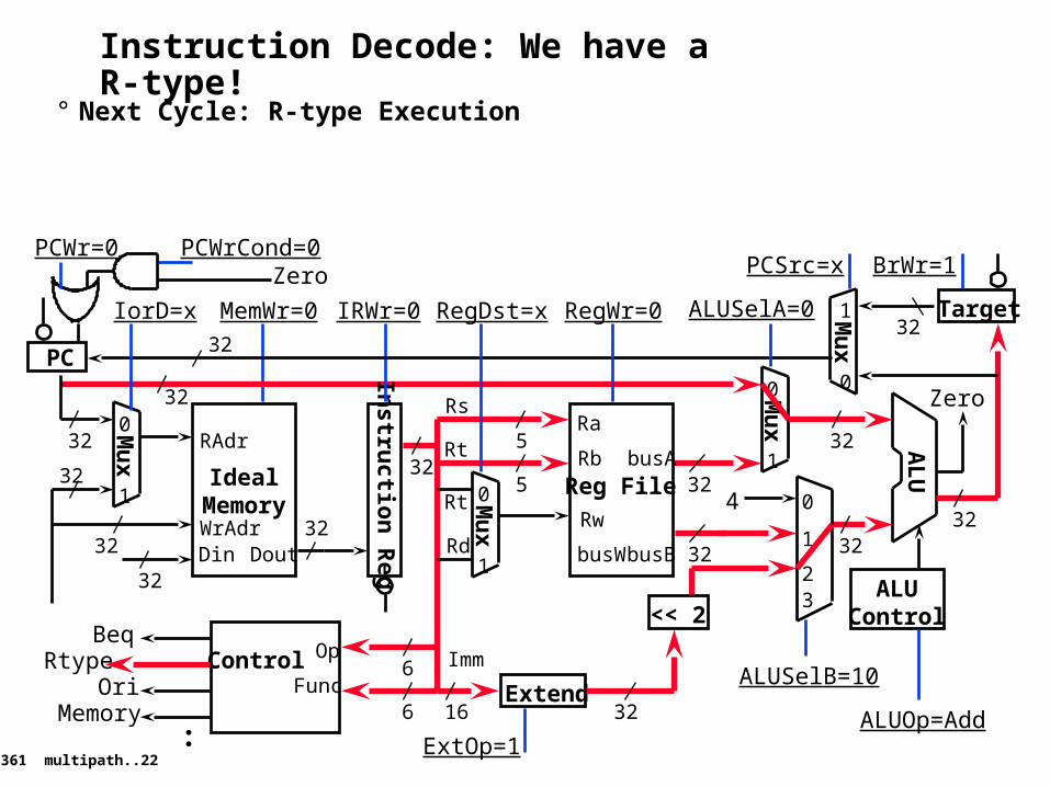
Instruction Decode: We have a R-type!
° Next Cycle: R-type Execution
Target
IdealMemoryWrAdrDin
RAdr
32
32
32Dout
MemWr=0
32
AL
U
3232
ALUOp=Add
ALUControl
Instru
ction R
eg
32
IRWr=0
32
Reg File
Ra
Rw
busW
Rb5
5
32busA
32busB
RegWr=0
Rs
Rt
Mu
x
0
1
Rt
Rd
PCWr=0
ALUSelA=0RegDst=x
Mu
x
0
1
32
PC
Extend
ExtOp=1
Mu
x
0
132
0
1
23
4
16
Imm
32
<< 2
ALUSelB=10
Mu
x
1
0
32
Zero
ZeroPCWrCond=0
PCSrc=x BrWr=1
32
IorD=x
Func
OpControl 6
6
BeqRtype
OriMemory
:
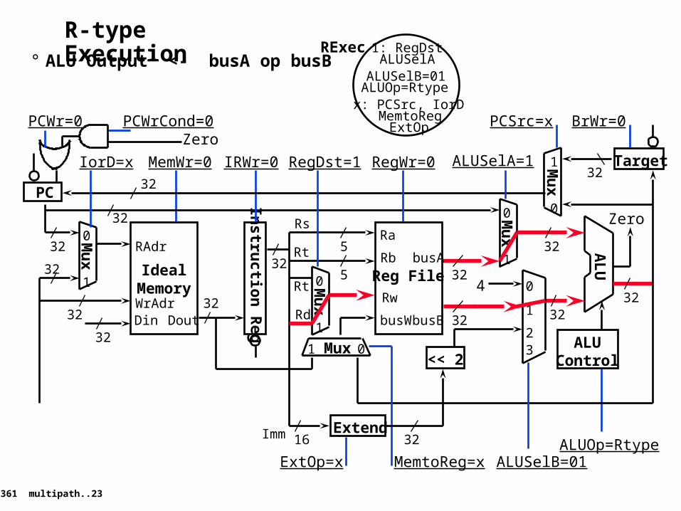
361 multipath..23
R-type Execution° ALU Output <- busA op busB
IdealMemoryWrAdrDin
RAdr
32
32
32Dout
MemWr=0
32
AL
U
3232
ALUOp=Rtype
ALUControl
Instru
ction R
eg
32
IRWr=0
32
Reg File
Ra
Rw
busW
Rb5
5
32busA
32busB
RegWr=0
Rs
Rt
Mu
x
0
1
Rt
Rd
PCWr=0
ALUSelA=1
Mux 01
RegDst=1
Mu
x
0
1
32
PC
MemtoReg=x
Extend
ExtOp=x
Mu
x
0
132
0
1
23
4
16Imm 32
<< 2
ALUSelB=01
Mu
x
1
0
Target32
Zero
ZeroPCWrCond=0 PCSrc=x BrWr=0
32
IorD=x
1: RegDst
ALUOp=RtypeALUSelB=01
x: PCSrc, IorDMemtoReg
ALUSelA
ExtOp
RExec
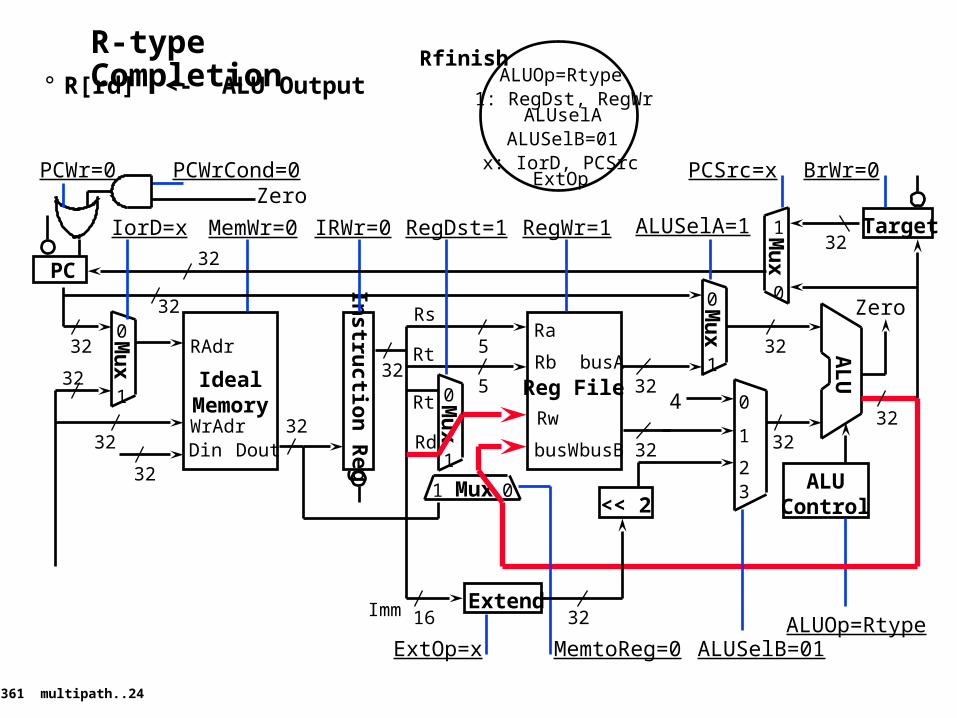
361 multipath..24
R-type Completion° R[rd] <- ALU Output
IdealMemoryWrAdrDin
RAdr
32
32
32Dout
MemWr=0
32
AL
U
3232
ALUOp=Rtype
ALUControl
Instru
ction R
eg
32
IRWr=0
32
Reg File
Ra
Rw
busW
Rb5
5
32busA
32busB
RegWr=1
Rs
Rt
Mu
x
0
1
Rt
Rd
PCWr=0
ALUSelA=1
Mux 01
RegDst=1
Mu
x
0
1
32
PC
MemtoReg=0
Extend
ExtOp=x
Mu
x
0
132
0
1
23
4
16Imm 32
<< 2
ALUSelB=01
Mu
x
1
0
Target32
Zero
ZeroPCWrCond=0 PCSrc=x BrWr=0
32
IorD=x
1: RegDst, RegWrALUOp=Rtype
ALUselA
x: IorD, PCSrcALUSelB=01
ExtOp
Rfinish
361 multipath..25
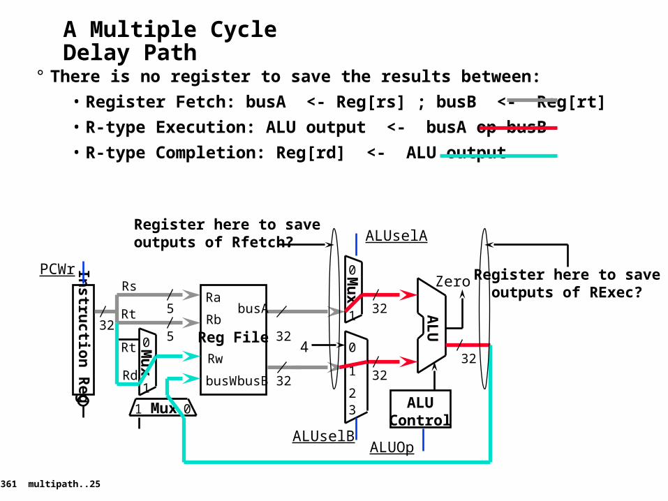
A Multiple Cycle Delay Path
° There is no register to save the results between:
• Register Fetch: busA <- Reg[rs] ; busB <- Reg[rt]
• R-type Execution: ALU output <- busA op busB
• R-type Completion: Reg[rd] <- ALU output
AL
U
3232
ALUControl
Instru
ction R
eg
32Reg File
Ra
Rw
busW
Rb5
5
32
busA
32busB
Rs
Rt
Mu
x
0
1
Rt
Rd
Mux 01
Mu
x
0
132
0
1
23
4
ZeroPCWr
ALUselA
ALUselB
Register here to saveoutputs of Rfetch?
Register here to saveoutputs of RExec?
ALUOp
361 multipath..26
A Multiple Cycle Delay Path (Continue)
° Register is NOT needed to save the outputs of Register Fetch:
• IRWr = 0: busA and busB will not change after Register Fetch
° Register is NOT needed to save the outputs of R-type Execution:
• busA and busB will not change after Register Fetch
• Control signals ALUSelA, ALUSelB, and ALUOpwill not change after R-type Execution
• Consequently ALU output will not change after R-type Execution
° In theory (P. 316, P&H), you need a register to hold a signal value if:
• (1) The signal is computed in one clock cycle and used in another.
• (2) AND the inputs to the functional block that computes this signal
can change before the signal is written into a state element.
° You can save a register if Cond 1 is true BUT Cond 2 is false:
• But in practice, this will introduce a multiple cycle delay path:
- A logic delay path that takes multiple cycles to propagate from one storage element to the next storage element
361 multipath..27
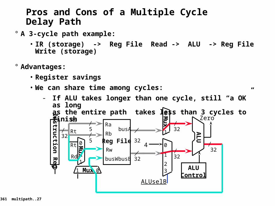
Pros and Cons of a Multiple Cycle Delay Path
° A 3-cycle path example:
• IR (storage) -> Reg File Read -> ALU -> Reg File Write (storage)
° Advantages:
• Register savings
• We can share time among cycles:
- If ALU takes longer than one cycle, still “a OK” as longas the entire path takes less than 3 cycles to finish
AL
U
3232
ALUControl
Instru
ction R
eg
32Reg File
Ra
Rw
busW
Rb5
5
32
busA
32busB
Rs
Rt
Mu
x
0
1
Rt
Rd
Mux 01
Mu
x0
132
0
1
23
4
Zero
ALUselB
361 multipath..28
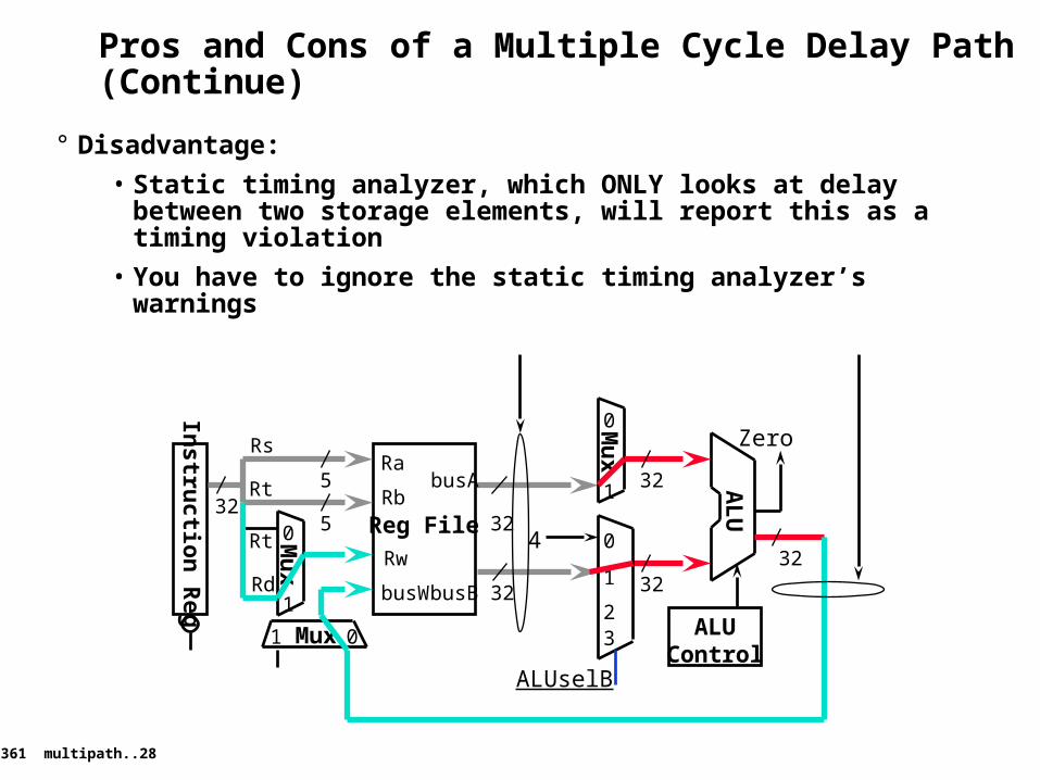
Pros and Cons of a Multiple Cycle Delay Path (Continue)
° Disadvantage:
• Static timing analyzer, which ONLY looks at delay between two storage elements, will report this as a timing violation
• You have to ignore the static timing analyzer’s warnings
AL
U
3232
ALUControl
Instru
ction R
eg
32Reg File
Ra
Rw
busW
Rb5
5
32
busA
32busB
Rs
Rt
Mu
x
0
1
Rt
Rd
Mux 01
Mu
x0
132
0
1
23
4
Zero
ALUselB
361 multipath..29
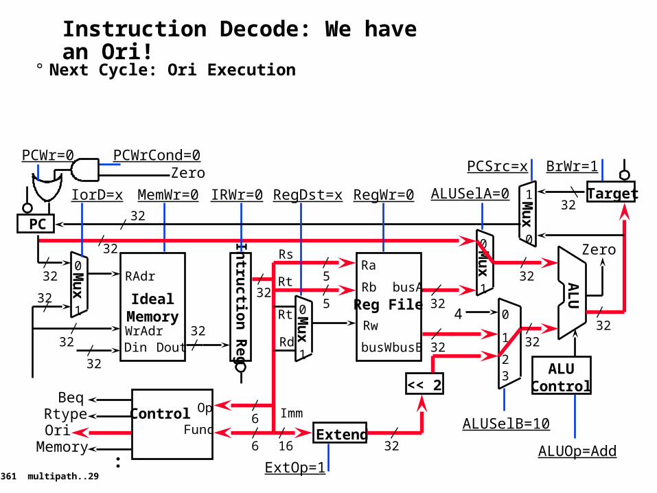
Instruction Decode: We have an Ori!
° Next Cycle: Ori Execution
Target
IdealMemoryWrAdrDin
RAdr
32
32
32Dout
MemWr=0
32
AL
U
3232
ALUOp=Add
ALUControl
Intru
ction R
eg
32
IRWr=0
32
Reg File
Ra
Rw
busW
Rb5
5
32busA
32busB
RegWr=0
Rs
Rt
Mu
x
0
1
Rt
Rd
PCWr=0
ALUSelA=0RegDst=x
Mu
x
0
1
32
PC
Extend
ExtOp=1
Mu
x
0
132
0
1
23
4
16
Imm
32
<< 2
ALUSelB=10
Mu
x
1
0
32
Zero
ZeroPCWrCond=0
PCSrc=x BrWr=1
32
IorD=x
Func
OpControl 6
6
BeqRtypeOri
Memory:
361 multipath..30
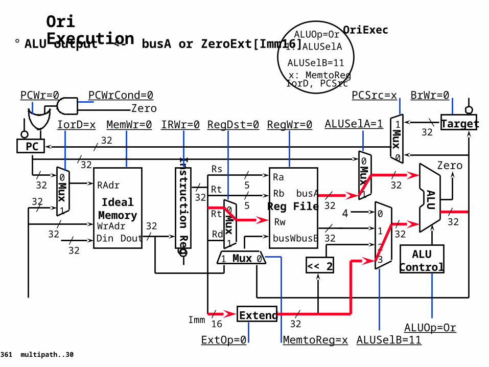
Ori Execution° ALU output <- busA or ZeroExt[Imm16]
IdealMemoryWrAdrDin
RAdr
32
32
32Dout
MemWr=0
32
AL
U
3232
ALUOp=Or
ALUControl
Instru
ction R
eg
32
IRWr=0
32
Reg File
Ra
Rw
busW
Rb5
5
32busA
32busB
RegWr=0
Rs
Rt
Mu
x
0
1
Rt
Rd
PCWr=0
ALUSelA=1
Mux 01
RegDst=0
Mu
x
0
1
32
PC
MemtoReg=x
Extend
ExtOp=0
Mu
x
0
132
0
1
23
4
16Imm 32
<< 2
ALUSelB=11
Mu
x
1
0
Target32
Zero
ZeroPCWrCond=0 PCSrc=x BrWr=0
32
IorD=x
ALUOp=Or
IorD, PCSrc
1: ALUSelA
ALUSelB=11x: MemtoReg
OriExec
361 multipath..31
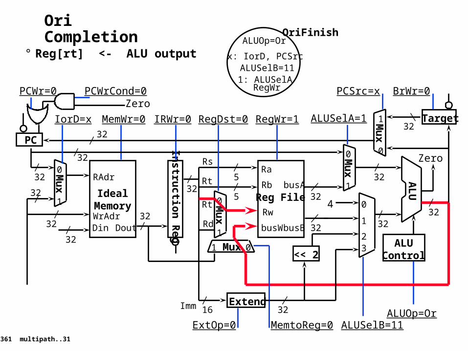
Ori Completion
° Reg[rt] <- ALU output
IdealMemoryWrAdrDin
RAdr
32
32
32Dout
MemWr=0
32
AL
U
3232
ALUOp=Or
ALUControl
Instru
ction R
eg
32
IRWr=0
32
Reg File
Ra
Rw
busW
Rb5
5
32busA
32busB
RegWr=1
Rs
Rt
Mu
x
0
1
Rt
Rd
PCWr=0
ALUSelA=1
Mux 01
RegDst=0
Mu
x
0
1
32
PC
MemtoReg=0
Extend
ExtOp=0
Mu
x
0
132
0
1
23
4
16Imm 32
<< 2
ALUSelB=11
Mu
x
1
0
Target32
Zero
ZeroPCWrCond=0 PCSrc=x BrWr=0
32
IorD=x
1: ALUSelA
ALUOp=Or
x: IorD, PCSrc
RegWr
ALUSelB=11
OriFinish
361 multipath..32
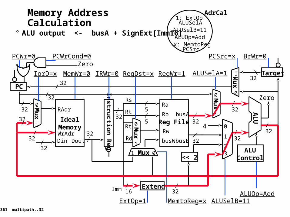
Memory Address Calculation
° ALU output <- busA + SignExt[Imm16]
IdealMemoryWrAdrDin
RAdr
32
32
32Dout
MemWr=0
32
AL
U
3232
ALUOp=Add
ALUControl
Instru
ction R
eg
32
IRWr=0
32
Reg File
Ra
Rw
busW
Rb5
5
32busA
32busB
RegWr=1
Rs
Rt
Mu
x
0
1
Rt
Rd
PCWr=0
ALUSelA=1
Mux 01
RegDst=x
Mu
x
0
1
32
PC
MemtoReg=x
Extend
ExtOp=1
Mu
x
0
132
0
1
23
4
16Imm 32
<< 2
ALUSelB=11
Mu
x
1
0
Target32
Zero
ZeroPCWrCond=0 PCSrc=x BrWr=0
32
IorD=x
ALUOp=Add
PCSrc
1: ExtOp
ALUSelB=11
x: MemtoReg
ALUSelA
AdrCal
361 multipath..33
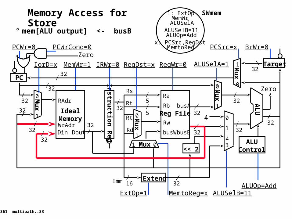
Memory Access for Store
° mem[ALU output] <- busB
IdealMemoryWrAdrDin
RAdr
32
32
32Dout
MemWr=1
32
AL
U
3232
ALUOp=Add
ALUControl
Instru
ction R
eg
32
IRWr=0
32
Reg File
Ra
Rw
busW
Rb5
5
32busA
32busB
RegWr=0
Rs
Rt
Mu
x
0
1
Rt
Rd
PCWr=0
ALUSelA=1
Mux 01
RegDst=x
Mu
x
0
1
32
PC
MemtoReg=x
Extend
ExtOp=1
Mu
x
0
132
0
1
23
4
16Imm 32
<< 2
ALUSelB=11
Mu
x1
0
Target32
Zero
ZeroPCWrCond=0 PCSrc=x BrWr=0
32
IorD=x
ALUOp=Addx: PCSrc,RegDst
1: ExtOp
ALUSelB=11
MemtoReg
MemWrALUSelA
SWmem
361 multipath..34
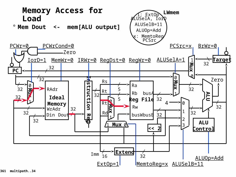
Memory Access for Load
° Mem Dout <- mem[ALU output]
IdealMemoryWrAdrDin
RAdr
32
32
32Dout
MemWr=0
32
AL
U
3232
ALUOp=Add
ALUControl
Instru
ction R
eg
32
IRWr=0
32
Reg File
Ra
Rw
busW
Rb5
5
32busA
32busB
RegWr=0
Rs
Rt
Mu
x
0
1
Rt
Rd
PCWr=0
ALUSelA=1
Mux 01
RegDst=0
Mu
x
0
1
32
PC
MemtoReg=x
Extend
ExtOp=1
Mu
x
0
132
0
1
23
4
16Imm 32
<< 2
ALUSelB=11
Mu
x
1
0
Target32
Zero
ZeroPCWrCond=0 PCSrc=x BrWr=0
32
IorD=1
ALUOp=Addx: MemtoReg
1: ExtOp
ALUSelB=11ALUSelA, IorD
PCSrc
LWmem
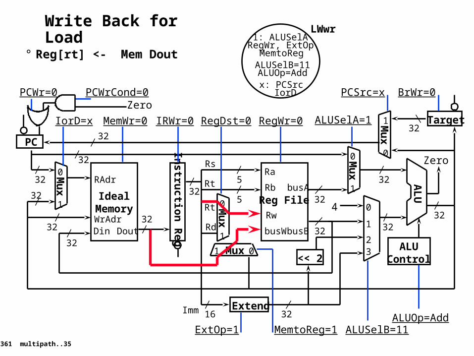
361 multipath..35
Write Back for Load
° Reg[rt] <- Mem Dout
IdealMemoryWrAdrDin
RAdr
32
32
32Dout
MemWr=0
32
AL
U
3232
ALUOp=Add
ALUControl
Instru
ction R
eg
32
IRWr=0
32
Reg File
Ra
Rw
busW
Rb5
5
32busA
32busB
RegWr=0
Rs
Rt
Mu
x
0
1
Rt
Rd
PCWr=0
ALUSelA=1
Mux 01
RegDst=0
Mu
x
0
1
32
PC
MemtoReg=1
Extend
ExtOp=1
Mu
x
0
132
0
1
23
4
16Imm 32
<< 2
ALUSelB=11
Mu
x
1
0
Target32
Zero
ZeroPCWrCond=0 PCSrc=x BrWr=0
32
IorD=x
ALUOp=Addx: PCSrc
1: ALUSelA
ALUSelB=11MemtoReg
RegWr, ExtOp
IorD
LWwr
361 multipath..36
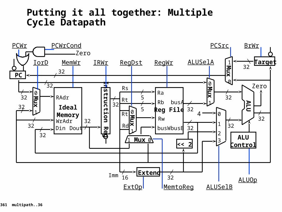
Putting it all together: Multiple Cycle Datapath
IdealMemoryWrAdrDin
RAdr
32
32
32Dout
MemWr
32
AL
U
3232
ALUOp
ALUControl
Instru
ction R
eg
32
IRWr
32
Reg File
Ra
Rw
busW
Rb5
5
32busA
32busB
RegWr
Rs
Rt
Mu
x
0
1
Rt
Rd
PCWr
ALUSelA
Mux 01
RegDst
Mu
x
0
1
32
PC
MemtoReg
Extend
ExtOp
Mu
x
0
132
0
1
23
4
16Imm 32
<< 2
ALUSelB
Mu
x1
0
Target32
Zero
ZeroPCWrCond PCSrc BrWr
32
IorD
361 multipath..37
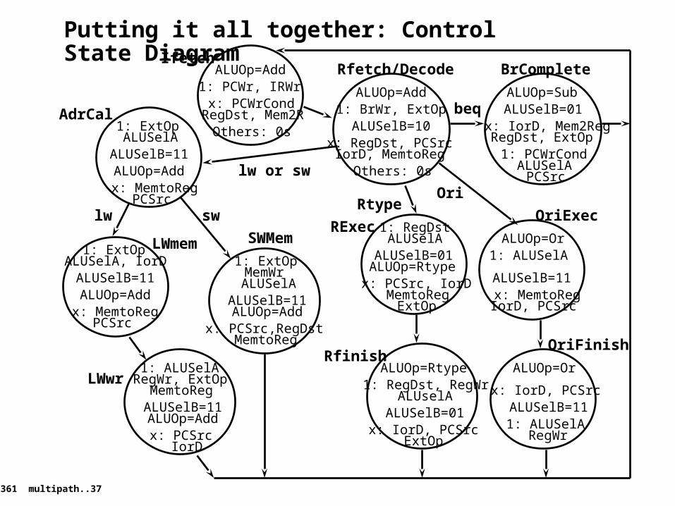
Putting it all together: Control State Diagram
1: PCWr, IRWrALUOp=Add
Others: 0s
x: PCWrCondRegDst, Mem2R
Ifetch
1: BrWr, ExtOpALUOp=Add
Others: 0s
x: RegDst, PCSrcALUSelB=10
IorD, MemtoReg
Rfetch/Decode
1: PCWrCond
ALUOp=Sub
x: IorD, Mem2RegALUSelB=01
RegDst, ExtOp
ALUSelA
BrComplete
PCSrc
1: RegDst
ALUOp=RtypeALUSelB=01
x: PCSrc, IorDMemtoReg
ALUSelA
ExtOp
RExec
1: RegDst, RegWrALUOp=Rtype
ALUselA
x: IorD, PCSrcALUSelB=01
ExtOp
Rfinish
ALUOp=Or
IorD, PCSrc
1: ALUSelA
ALUSelB=11x: MemtoReg
OriExec
1: ALUSelA
ALUOp=Or
x: IorD, PCSrc
RegWr
ALUSelB=11
OriFinish
ALUOp=Add
PCSrc
1: ExtOp
ALUSelB=11
x: MemtoReg
ALUSelA
AdrCal
ALUOp=Addx: PCSrc,RegDst
1: ExtOp
ALUSelB=11
MemtoReg
MemWrALUSelA
SWMem
ALUOp=Addx: MemtoReg
1: ExtOp
ALUSelB=11ALUSelA, IorD
PCSrc
LWmem
ALUOp=Addx: PCSrc
1: ALUSelA
ALUSelB=11MemtoReg
RegWr, ExtOp
IorD
LWwr
lw or sw
lw swRtype
Ori
beq
361 multipath..38
Summary
° Disadvantages of the Single Cycle Processor
• Long cycle time
• Cycle time is too long for all instructions except the Load
° Multiple Cycle Processor:
• Divide the instructions into smaller steps
• Execute each step (instead of the entire instruction) in one cycle
° Do NOT confuse Multiple Cycle Processor with Multiple Cycle Delay Path
• Multiple Cycle Processor executes eachinstruction in multiple clock cycles
• Multiple Cycle Delay Path: a combinational logic path between two storage elements that takes more than one clock cycle to complete
° It is possible (desirable) to build a MC Processor without MCDP:
• Use a register to save a signal’s value whenever a signal is generated in one clock cycle and used in another cycle later