3680 series universal test fixture operation and ... · 1-1 introduction this manual provides...
TRANSCRIPT

Operation and Maintenance Manual
3680 SeriesUniversal Test Fixture Operation and Maintenance Manual3680 Universal Test Fixture36801K and 36801V Right-Angle Launchers36803 Bias Probe36802 MMIC Attachment36805-10M, 36805-15M, and 36805-25M Substrate Kits
36804B-10M 0.25 mm (10 mil) Microstrip Calibration/Verification Kit36804B-15M 0.38 mm (15 mil) Microstrip Calibration/Verification Kit36804B-25M 0.63 mm (25 mil) Microstrip Calibration/Verification Kit36804-25C 0.63 mm (25 mil) CPW
Anritsu Company490 Jarvis DriveMorgan Hill, CA 95037-2809USAhttp://www.anritsu.com
Part Number: 10410-00064Revision: K
Published: March 2019Copyright 2019 Anritsu Company, USA. All Rights Reserved.

WARRANTYThe Anritsu product(s) listed on the title page is (are) warranted against defects in materials and workmanship for90 days from the date of shipment.
Anritsu’s obligation covers repairing or replacing products which prove to be defective during the warranty period.Buyers shall prepay transportation charges for equipment returned to Anritsu for warranty repairs. Obligation islimited to the original purchaser. Anritsu is not liable for consequential damages.
LIMITATION OF WARRANTYThe foregoing warranty does not apply to Anritsu connectors that have failed due to normal wear. Also, the warrantydoes not apply to defects resulting from improper or inadequate maintenance, unauthorized modification or misuse,or operation outside of the environmental specifications of the product. No other warranty is expressed or implied,and the remedies provided herein are the Buyer’s sole and exclusive remedies.
DISCLAIMER OF WARRANTY DISCLAIMER OF WARRANTIES. TO THE MAXIMUM EXTENT PERMITTED BY APPLICABLE LAW, ANRITSUCOMPANY AND ITS SUPPLIERS DISCLAIM ALL WARRANTIES, EITHER EXPRESSED OR IMPLIED,INCLUDING, BUT NOT LIMITED TO, IMPLIED WARRANTIES OF MERCHANTABILITY AND FITNESS FOR APARTICULAR PURPOSE, WITH REGARD TO THE PRODUCT. THE USER ASSUMES THE ENTIRE RISK OFUSING THE PRODUCT. ANY LIABILITY OF PROVIDER OR MANUFACTURER WILL BE LIMITEDEXCLUSIVELY TO PRODUCT REPLACEMENT.
NO LIABILITY FOR CONSEQUENTIAL DAMAGES. TO THE MAXIMUM EXTENT PERMITTED BYAPPLICABLE LAW, IN NO EVENT SHALL ANRITSU COMPANY OR ITS SUPPLIERS BE LIABLE FOR ANYSPECIAL, INCIDENTAL, INDIRECT, OR CONSEQUENTIAL DAMAGES WHATSOEVER (INCLUDING,WITHOUT LIMITATION, DAMAGES FOR LOSS OF BUSINESS PROFITS, BUSINESS INTERRUPTION, LOSSOF BUSINESS INFORMATION, OR ANY OTHER PECUNIARY LOSS) ARISING OUT OF THE USE OF ORINABILITY TO USE THE PRODUCT, EVEN IF ANRITSU COMPANY HAS BEEN ADVISED OF THEPOSSIBILITY OF SUCH DAMAGES. BECAUSE SOME STATES AND JURISDICTIONS DO NOT ALLOW THEEXCLUSION OR LIMITATION OF LIABILITY FOR CONSEQUENTIAL OR INCIDENTAL DAMAGES, THEABOVE LIMITATION MAY NOT APPLY TO YOU.
TRADEMARK ACKNOWLEDGMENTSK Connector and V Connector are trademarks of the Anritsu Company.
RT/duroid® is a registered trademark of Rogers Corporation.
Eccosorb® is a registered trademark of Emerson & Cumming Inc., a unit of Laird Technologies
NOTICEAnritsu Company has prepared this manual for use by Anritsu Company personnel and customers as a guide for theproper installation, operation and maintenance of Anritsu Company equipment and computer programs. Thedrawings, specifications, and information contained herein are the property of Anritsu Company, and anyunauthorized use or disclosure of these drawings, specifications, and information is prohibited; they shall not bereproduced, copied, or used in whole or in part as the basis for manufacture or sale of the equipment or softwareprograms without the prior written consent of Anritsu Company.
UPDATESUpdates, if any, can be downloaded from the Documents area of the Anritsu Website at:http://www.anritsu.com
For the latest service and sales contact information in your area, please visit:http://www.anritsu.com/contact
Notes On Export ManagementThis product and its manuals may require an Export License or approval by the government of the product country of origin for re-export from your country.
Before you export this product or any of its manuals, please contact Anritsu Company to confirm whether or not these items are export-controlled.
When disposing of export-controlled items, the products and manuals need to be broken or shredded to such a degree that they cannot be unlawfully used for military purposes.

European Parliament and Council Directive 2002/96/EC
Chinese RoHS Compliance Statement
Equipment Marked with the crossed-out WheelieBin symbol complies with the European
Parliament and Council Directive 2002/96/EC (the“WEEE Directive”) in the European Union.
For Products placed on the EU market afterAugust 13, 2005, please contact your local Anritsurepresentative at the end of the product’s usefullife to arrange disposal in accordance with your
initial contract and the local law.


3680 UTF OMM PN: 10410-00064 Rev. H Safety-1
Safety SymbolsTo prevent the risk of personal injury or loss related to equipment malfunction, Anritsu Company uses the following symbols to indicate safety-related information. For your own safety, please read the information carefully before operating the equipment.
Symbols Used in Manuals
Safety Symbols Used on Equipment and in ManualsThe following safety symbols are used inside or on the equipment near operation locations to provide information about safety items and operation precautions. Ensure that you clearly understand the meanings of the symbols and take the necessary precautions before operating the equipment. Some or all of the following five symbols may or may not be used on all Anritsu equipment. In addition, there may be other labels attached to products that are not shown in the diagrams in this manual.
Danger
This indicates a risk from a very dangerous condition or procedure that could result in serious injury or death and possible loss related to equipment malfunction. Follow all precautions and procedures to minimize this risk.
WarningThis indicates a risk from a hazardous condition or procedure that could result in light-to-severe injury or loss related to equipment malfunction. Follow all precautions and procedures to minimize this risk.
Caution
This indicates a risk from a hazardous procedure that could result in loss related to equipment malfunction. Follow all precautions and procedures to minimize this risk.
This indicates a prohibited operation. The prohibited operation is indicated symbolically in or near the barred circle.
This indicates a compulsory safety precaution. The required operation is indicated symbolically in or near the circle.
This indicates a warning or caution. The contents are indicated symbolically in or near the triangle.
This indicates a note. The contents are described in the box.
These indicate that the marked part should be recycled.

Safety-2 PN: 10410-00064 Rev. K 3680 UTF OMM
For Safety
Warning Always refer to the operation manual when working near locations at which the alert mark, shown on the left, is attached. If the operation, etc., is performed without heeding the advice in the operation manual, there is a risk of personal injury. In addition, the equipment performance may be reduced.
Moreover, this alert mark is sometimes used with other marks and descriptions indicating other dangers.
Caution
Electrostatic Discharge (ESD) can damage the highly sensitive circuits in the instrument. ESD is most likely to occur as test devices are being connected to, or disconnected from, the instrument’s front and rear panel ports and connectors. You can protect the instrument and test devices by wearing a static-discharge wristband. Alternatively, you can ground yourself to discharge any static charge by touching the outer chassis of the grounded instrument before touching the instrument’s front and rear panel ports and connectors. Avoid touching the test port center conductors unless you are properly grounded and have eliminated the possibility of static discharge.
Repair of damage that is found to be caused by electrostatic discharge is not covered under warranty.
3680 UTF OMM PN: 10410-00064 Rev. K Contents-1
Table of Contents
Chapter 1—General Information
1-1 Introduction. . . . . . . . . . . . . . . . . . . . . . . . . . . . . . . . . . . . . . . . . . . . . . . . . . . . . . . . . . . . . . . . 1-1
1-2 General Description . . . . . . . . . . . . . . . . . . . . . . . . . . . . . . . . . . . . . . . . . . . . . . . . . . . . . . . . . 1-1
1-3 Optional Accessories . . . . . . . . . . . . . . . . . . . . . . . . . . . . . . . . . . . . . . . . . . . . . . . . . . . . . . . . 1-1
Model 36801 Right Angle Launcher . . . . . . . . . . . . . . . . . . . . . . . . . . . . . . . . . . . . . . . . . . 1-1
Model 36803 Bias Probe . . . . . . . . . . . . . . . . . . . . . . . . . . . . . . . . . . . . . . . . . . . . . . . . . . . 1-2
Model 36802 MMIC Attachment . . . . . . . . . . . . . . . . . . . . . . . . . . . . . . . . . . . . . . . . . . . . . 1-2
1-4 UTF Component Descriptions . . . . . . . . . . . . . . . . . . . . . . . . . . . . . . . . . . . . . . . . . . . . . . . . . 1-3
1-5 Optional Accessories . . . . . . . . . . . . . . . . . . . . . . . . . . . . . . . . . . . . . . . . . . . . . . . . . . . . . . . . 1-5
Model 36801 Right Angle Launcher . . . . . . . . . . . . . . . . . . . . . . . . . . . . . . . . . . . . . . . . . . 1-5
Model 36803 Bias Probe. . . . . . . . . . . . . . . . . . . . . . . . . . . . . . . . . . . . . . . . . . . . . . . . . . . 1-5
Model 36802 MMIC Attachment. . . . . . . . . . . . . . . . . . . . . . . . . . . . . . . . . . . . . . . . . . . . . . 1-5
1-6 3680 UTF Technical Data. . . . . . . . . . . . . . . . . . . . . . . . . . . . . . . . . . . . . . . . . . . . . . . . . . . . . 1-6
Chapter 2—Operation
2-1 Introduction. . . . . . . . . . . . . . . . . . . . . . . . . . . . . . . . . . . . . . . . . . . . . . . . . . . . . . . . . . . . . . . . 2-1
2-2 Operation with Scalar Network Analyzer Systems . . . . . . . . . . . . . . . . . . . . . . . . . . . . . . . . . . 2-1
Calibration . . . . . . . . . . . . . . . . . . . . . . . . . . . . . . . . . . . . . . . . . . . . . . . . . . . . . . . . . . . . . . 2-1
Equipment Setup . . . . . . . . . . . . . . . . . . . . . . . . . . . . . . . . . . . . . . . . . . . . . . . . . . . . . . . . . 2-1
Substrate Mounting Procedure . . . . . . . . . . . . . . . . . . . . . . . . . . . . . . . . . . . . . . . . . . . . . . 2-1
Measurement. . . . . . . . . . . . . . . . . . . . . . . . . . . . . . . . . . . . . . . . . . . . . . . . . . . . . . . . . . . . 2-2
2-3 Operation with Vector Network Analyzer Systems . . . . . . . . . . . . . . . . . . . . . . . . . . . . . . . . . . 2-3
Equipment Setup . . . . . . . . . . . . . . . . . . . . . . . . . . . . . . . . . . . . . . . . . . . . . . . . . . . . . . . . . 2-3
Substrate Mounting Procedure . . . . . . . . . . . . . . . . . . . . . . . . . . . . . . . . . . . . . . . . . . . . . . 2-4
Calibration . . . . . . . . . . . . . . . . . . . . . . . . . . . . . . . . . . . . . . . . . . . . . . . . . . . . . . . . . . . . . . 2-4
Measurement. . . . . . . . . . . . . . . . . . . . . . . . . . . . . . . . . . . . . . . . . . . . . . . . . . . . . . . . . . . . 2-4
2-4 CPW Measurement Considerations . . . . . . . . . . . . . . . . . . . . . . . . . . . . . . . . . . . . . . . . . . . . . 2-5
2-5 Measurements of Carrier Mounted Substrate. . . . . . . . . . . . . . . . . . . . . . . . . . . . . . . . . . . . . . 2-5
2-6 Use of the Substrate Stop. . . . . . . . . . . . . . . . . . . . . . . . . . . . . . . . . . . . . . . . . . . . . . . . . . . . . 2-5
Chapter 3—Calibration
3-1 Introduction. . . . . . . . . . . . . . . . . . . . . . . . . . . . . . . . . . . . . . . . . . . . . . . . . . . . . . . . . . . . . . . . 3-1
3-2 General Information . . . . . . . . . . . . . . . . . . . . . . . . . . . . . . . . . . . . . . . . . . . . . . . . . . . . . . . . . 3-1
3-3 Calibration Verification Kits. . . . . . . . . . . . . . . . . . . . . . . . . . . . . . . . . . . . . . . . . . . . . . . . . . . . 3-1
Calibration Kit Components. . . . . . . . . . . . . . . . . . . . . . . . . . . . . . . . . . . . . . . . . . . . . . . . . 3-2
3-4 Calibration for Microstrip. . . . . . . . . . . . . . . . . . . . . . . . . . . . . . . . . . . . . . . . . . . . . . . . . . . . . . 3-3
Line-Reflect-Line (LRL) Calibration . . . . . . . . . . . . . . . . . . . . . . . . . . . . . . . . . . . . . . . . . . . 3-3
Line-Reflect-Match Calibration . . . . . . . . . . . . . . . . . . . . . . . . . . . . . . . . . . . . . . . . . . . . . . 3-4
Three-Line LRL Calibration and Combined LRL/LRM Calibration. . . . . . . . . . . . . . . . . . . . 3-5
Open-Short-Load Calibration. . . . . . . . . . . . . . . . . . . . . . . . . . . . . . . . . . . . . . . . . . . . . . . . 3-5
Recalibration with a Stored Calibration . . . . . . . . . . . . . . . . . . . . . . . . . . . . . . . . . . . . . . . . 3-5
3-5 Calibration for CPW . . . . . . . . . . . . . . . . . . . . . . . . . . . . . . . . . . . . . . . . . . . . . . . . . . . . . . . . . 3-6

Contents-2 PN: 10410-00064 Rev. K 3680 UTF OMM
Table of Contents (Continued)
3-6 Calibration Checks . . . . . . . . . . . . . . . . . . . . . . . . . . . . . . . . . . . . . . . . . . . . . . . . . . . . . . . . . . 3-7
Measurement of Calibration Standards . . . . . . . . . . . . . . . . . . . . . . . . . . . . . . . . . . . . . . . . 3-7
Measurement of Known Standards . . . . . . . . . . . . . . . . . . . . . . . . . . . . . . . . . . . . . . . . . . . 3-7
Measurement of Assurance Standards . . . . . . . . . . . . . . . . . . . . . . . . . . . . . . . . . . . . . . . . 3-8
3-7 RF Measurement Chart . . . . . . . . . . . . . . . . . . . . . . . . . . . . . . . . . . . . . . . . . . . . . . . . . . . . . . 3-9
Chapter 4—Maintenance
4-1 Introduction . . . . . . . . . . . . . . . . . . . . . . . . . . . . . . . . . . . . . . . . . . . . . . . . . . . . . . . . . . . . . . . . 4-1
4-2 Upper Jaw Adjustment . . . . . . . . . . . . . . . . . . . . . . . . . . . . . . . . . . . . . . . . . . . . . . . . . . . . . . . 4-1
Jaw Types . . . . . . . . . . . . . . . . . . . . . . . . . . . . . . . . . . . . . . . . . . . . . . . . . . . . . . . . . . . . . . 4-1
Adjustment Block . . . . . . . . . . . . . . . . . . . . . . . . . . . . . . . . . . . . . . . . . . . . . . . . . . . . . . . . . 4-1
Required Tools . . . . . . . . . . . . . . . . . . . . . . . . . . . . . . . . . . . . . . . . . . . . . . . . . . . . . . . . . . 4-1
Adjustment Steps. . . . . . . . . . . . . . . . . . . . . . . . . . . . . . . . . . . . . . . . . . . . . . . . . . . . . . . . . 4-1
4-3 Connector Removal and Replacement . . . . . . . . . . . . . . . . . . . . . . . . . . . . . . . . . . . . . . . . . . . 4-2
Required Tools . . . . . . . . . . . . . . . . . . . . . . . . . . . . . . . . . . . . . . . . . . . . . . . . . . . . . . . . . . 4-2
Connector Removal . . . . . . . . . . . . . . . . . . . . . . . . . . . . . . . . . . . . . . . . . . . . . . . . . . . . . . . 4-2
Connector Installation . . . . . . . . . . . . . . . . . . . . . . . . . . . . . . . . . . . . . . . . . . . . . . . . . . . . . 4-3
4-4 Preventive Maintenance . . . . . . . . . . . . . . . . . . . . . . . . . . . . . . . . . . . . . . . . . . . . . . . . . . . . . . 4-3
UTF Maintenance . . . . . . . . . . . . . . . . . . . . . . . . . . . . . . . . . . . . . . . . . . . . . . . . . . . . . . . . 4-3
Calibration Kit Maintenance. . . . . . . . . . . . . . . . . . . . . . . . . . . . . . . . . . . . . . . . . . . . . . . . . 4-3
Chapter 5—Using Optional Accessories
5-1 Introduction . . . . . . . . . . . . . . . . . . . . . . . . . . . . . . . . . . . . . . . . . . . . . . . . . . . . . . . . . . . . . . . . 5-1
5-2 Right-Angle Launcher . . . . . . . . . . . . . . . . . . . . . . . . . . . . . . . . . . . . . . . . . . . . . . . . . . . . . . . . 5-1
General Information . . . . . . . . . . . . . . . . . . . . . . . . . . . . . . . . . . . . . . . . . . . . . . . . . . . . . . . 5-1
Mounting . . . . . . . . . . . . . . . . . . . . . . . . . . . . . . . . . . . . . . . . . . . . . . . . . . . . . . . . . . . . . . . 5-1
Calibration . . . . . . . . . . . . . . . . . . . . . . . . . . . . . . . . . . . . . . . . . . . . . . . . . . . . . . . . . . . . . . 5-2
Measurement Setup . . . . . . . . . . . . . . . . . . . . . . . . . . . . . . . . . . . . . . . . . . . . . . . . . . . . . . 5-2
Upper Jaw Adjustment (if Required) . . . . . . . . . . . . . . . . . . . . . . . . . . . . . . . . . . . . . . . . . . 5-2
Multiport Measurements . . . . . . . . . . . . . . . . . . . . . . . . . . . . . . . . . . . . . . . . . . . . . . . . . . . 5-2
5-3 MMIC Attachment . . . . . . . . . . . . . . . . . . . . . . . . . . . . . . . . . . . . . . . . . . . . . . . . . . . . . . . . . . . 5-3
General Information . . . . . . . . . . . . . . . . . . . . . . . . . . . . . . . . . . . . . . . . . . . . . . . . . . . . . . . 5-3
Mounting . . . . . . . . . . . . . . . . . . . . . . . . . . . . . . . . . . . . . . . . . . . . . . . . . . . . . . . . . . . . . . . 5-4
Calibration . . . . . . . . . . . . . . . . . . . . . . . . . . . . . . . . . . . . . . . . . . . . . . . . . . . . . . . . . . . . . . 5-5
Measurement. . . . . . . . . . . . . . . . . . . . . . . . . . . . . . . . . . . . . . . . . . . . . . . . . . . . . . . . . . . . 5-5
5-4 Bias Probe . . . . . . . . . . . . . . . . . . . . . . . . . . . . . . . . . . . . . . . . . . . . . . . . . . . . . . . . . . . . . . . . 5-6
Using The Probe Assembly as a Bias Probe. . . . . . . . . . . . . . . . . . . . . . . . . . . . . . . . . . . . 5-6
Using the Probe Assembly as a Hold-down for Components . . . . . . . . . . . . . . . . . . . . . . . 5-6
Chapter 6—Applications
6-1 Introduction . . . . . . . . . . . . . . . . . . . . . . . . . . . . . . . . . . . . . . . . . . . . . . . . . . . . . . . . . . . . . . . . 6-1
6-2 UTF-to-Microstrip Connection Pin Design . . . . . . . . . . . . . . . . . . . . . . . . . . . . . . . . . . . . . . . . 6-1
6-3 Upper Jaw Modification. . . . . . . . . . . . . . . . . . . . . . . . . . . . . . . . . . . . . . . . . . . . . . . . . . . . . . . 6-2
6-4 Making LRL Calibration Lines . . . . . . . . . . . . . . . . . . . . . . . . . . . . . . . . . . . . . . . . . . . . . . . . . . 6-3

3680 UTF OMM PN: 10410-00064 Rev. K Contents-3
Table of Contents (Continued)
6-5 Measurement Considerations. . . . . . . . . . . . . . . . . . . . . . . . . . . . . . . . . . . . . . . . . . . . . . . . . . 6-3
Soft Substrate . . . . . . . . . . . . . . . . . . . . . . . . . . . . . . . . . . . . . . . . . . . . . . . . . . . . . . . . . . . 6-3
Substrate on Carriers . . . . . . . . . . . . . . . . . . . . . . . . . . . . . . . . . . . . . . . . . . . . . . . . . . . . . 6-3
Substrate of Different Thickness than the Calibration Substrate. . . . . . . . . . . . . . . . . . . . . 6-3
6-6 Substrate Moding . . . . . . . . . . . . . . . . . . . . . . . . . . . . . . . . . . . . . . . . . . . . . . . . . . . . . . . . . . . 6-4
Index

Contents-4 PN: 10410-00064 Rev. K 3680 UTF OMM
Table of Contents (Continued)

3680 UTF OMM PN: 10410-00064 Rev. K 1-1
Chapter 1 — General Information
1-1 IntroductionThis manual provides general information, operating instructions, calibration procedures, and maintenance information for the 3680 Series Universal Test Fixture (UTF) and optional accessories.
1-2 General DescriptionThe 3680 Series Universal Test Fixture supports on-substrate testing of microstrip and coplanar waveguide (CPW) devices. The test fixture accommodates a wide variety of sizes and configurations of these substrates. The test substrates are clamped directly into the launchers of the fixture eliminating the need for carrier blocks. By using the optional Model 36801 Right-Angle Launcher, up to four RF connections can be made on a substrate. Biasing connections can be made using the Model 36803 Bias Probes. The test fixture supports up to four bias probes. The optional Model 36802 MMIC Attachment enables the fixture to support testing of very small substrates or devices. The UTF can be used with either a scalar network analyzer (SNA) or a vector network analyzer (VNA). Calibration/Verification kits are available in a variety of formats (refer to Chapter 3, “Calibration”).
There are three models of the UTF; the Model 3680-20 which supports testing from DC to 20 GHz with the 3.5 mm Connector, the Model 3680K, which supports testing from DC to 40 GHz with the K Connector, and the Model 3680V, which supports testing from DC to 60 GHz with the V Connector.
The UTF is equipped as follows:
• Universal Test Fixture (Model 3680-20, 3680K or 3680V)
• Adjustment Block (for adjusting jaws)
• Substrate Stop (includes locating pin and screw)
• Connector Removal Tool
• Screwdriver, Phillips (not included with Model 3680-20)
• Wrenches, 5/16”, 2 each (not included with Model 3680-20)
• Wooden Box (Plastic Box for Model 3680-20)
1-3 Optional AccessoriesThe following optional accessories are available. Chapter 5, “Using Optional Accessories” provides details concerning their use.
Model 36801 Right Angle Launcher
The Right-Angle Launcher (RAL) is used to make multi-port connections as well as right angle connections to the test substrates. There are two models of the RAL; the Model 36801V which has a V Connector, and the Model 36801K which has a K Connector. The RAL is equipped as follows:
• Right-Angle Launcher (Model 36801K or 36801V)
• Adjustment Plate
• Mounting Base Assembly
• Hex Wrenches
• Wooden Box
1-3 Optional Accessories General Information
1-2 PN: 10410-00064 Rev. K 3680 UTF OMM
Model 36803 Bias Probe
The Bias Probe is used either as a bias probe or as a hold-down for components. When used as a hold-down, the dielectric probe is used. The Bias Probe is equipped as follows:
• Bias Probe Assembly
• Ground Cable Assembly
• Dielectric Probe
• Allen Wrenches
A 10 bias probe attachment is available as a special item.
Model 36802 MMIC Attachment
The MMIC Attachment is used to support testing of small substrates or devices and substrates where it is not feasible to make connections with the UTF jaws. The MMIC Attachment is equipped as follows:
• Cam Assemblies, 2 each
• Mounting Base Assembly
• Mounting Screws
• Wooden Box
A Model 36805-10M, 36805-15M, or 36805-25M Connection Substrate Kit is required and must be ordered separately. Model 36805-10M is for 10 mil substrates, 36805-15M is for 15 mil substrates, and 36805-25M is for 25 mil substrates. Each kit contains:
• Connection Substrate, 4 each
• Mounting Block, 1 each
• Pin Foot (Spare), 1 each
• Short, 2 each

General Information 1-4 UTF Component Descriptions
3680 UTF OMM PN: 10410-00064 Rev. K 1-3
1-4 UTF Component Descriptions The following is a list and description of the components that make up the UTF. See Figure 1-1 for the location of these components.
Index Name Description
1 RF Connector
Each UTF model has a different RF connector type installed:
3.5 mm Connector – supports testing from DC to 20 GHz (Model 3680-20)
K Connector – supports testing from DC to 40 GHz (Model 3680K)
V Connector – supports testing from DC to 60 GHz (Model 3680V)
The RF connectors have a front side where the external RF connection is made, and a back side which contains a center conductor pin. This center conductor pin makes a spring loaded pressure contact with the strip conductor of the substrate. The tip of the center conductor pin extends beyond the jaws, allowing visual alignment of the substrate into the fixture. The center conductor pins of the K Connector and V Connector have different designs (refer to Section 6-2 in Chapter 6). The RF connectors are field replaceable.
2 LeverUsed to open the lower jaws. Closing of the lower jaws is controlled by spring pressure.
3 Substrate StopAn adjustable stop which can be used to accurately position substrates of the same width.
Figure 1-1. UTF Component Descriptions (1 of 2)
MODEL 3680 V
FixedConnector
Block
Jaws SlidingConnector
Block
Slide Rod
Offset Block
RF Connector1 Lever2
SubstrateStop3
DielectricSpacerRods4
11
RF Connector6Lever5
9 10 12
Base7
8

1-4 UTF Component Descriptions General Information
1-4 PN: 10410-00064 Rev. K 3680 UTF OMM
4 Dielectric Spacer Rods
Used to space the substrate away from the connector block the precise distance required to compensate for the interface fringing capacitance. There are two dielectric rods behind each set of jaw plates. They are optimized for 10 mil substrates.
5 Lever Same as index 2
6 RF Connector Same as index 1
7 Base The support platform of the test fixture.
8 Fixed Connector Block The RF connector assembly that is firmly attached to the base.
9
JawsThe plates which clamp the substrate in position and provide the proper ground connections. They consist of the Fixed Upper Jaw and the Movable Lower Jaw.
Fixed Upper Jaw
The jaw which provides the stop that sets the correct pressure between the RF connector center conductor pin and the substrate strip conductor. The upper jaw also provides the ground connection when used with CPW. The upper jaw is adjustable and is aligned using the Alignment Block.
There are two types of upper jaws; one for microstrip and one for CPW. The microstrip upper jaw has two connector configurations; a semicircle configuration for most applications and a slot configuration for very narrow microstrip measurements. The UTF comes from the factory with microstrip upper jaws installed. The CPW upper jaws come as part of the CPW calibration kit.
Movable Lower Jaw
The jaw that is opened by the levers. It provides the spring loaded clamping of the substrate to the connector blocks. The lower jaw provides the proper ground for microstrip substrates.
The UTF comes with a thin sheet metal jaw separator installed between the upper and lower jaws. This relieves the pressure on the connector pin. It is good practice to install the separator whenever the UTF will not be used for a long period of time or is placed in storage. When installing the jaw separator, position it off center so that it does not contact the connector pin.
10 Sliding Connector BlockThe RF connector assembly which slides along the slide rods and allows adjustment for the length of the substrate. The slide lock screw locks this block in position.
11 Slide Rods The rods that support the sliding connector block.
12 Offset BlockThe assembly that holds the sliding rods and allows the RF connectors to be offset axially ±1/2 in (±1 in for Model 3680-20). The offset lock screw fixes the position of this block.
– Alignment Block(Not Shown) Used to precisely position the upper jaw of a connector block when the upper jaw is changed or adjusted.
Figure 1-1. UTF Component Descriptions (2 of 2)

General Information 1-5 Optional Accessories
3680 UTF OMM PN: 10410-00064 Rev. K 1-5
1-5 Optional Accessories The following optional accessories are available. Chapter 5 provides details concerning their use.
Model 36801 Right Angle Launcher
The Right Angle Launcher (RAL) is used to make multiport connections as well as right angle connections to the test substrates. There are two models of the RAL; the Model 36801V which has a V Connector, and the Model 36801K which has a K Connector. The RAL is equipped as follows:
• Right Angle Launcher (Model 36801K or 36801V)
• Adjustment Plate
• Mounting Base Assembly
• Hex Wrenches
• Wooden Box
Model 36803 Bias Probe.
The Bias Probe is used either as a bias probe or as a hold-down for components. When used as a hold-down, the dielectric probe is used. The Bias Probe is equipped as follows:
• Bias Probe Assembly
• Ground Cable Assembly
• Dielectric Probe
• Allen Wrenches
Model 36802 MMIC Attachment.
The MMIC Attachment is used to support testing of small substrates or devices and substrates where it is not feasible to make connections with the UTF jaws. The MMIC Attachment is equipped as follows:
• Cam Assemblies, 2 each
• Mounting Base Assembly
• Mounting Screws
• Wooden Box
A Model 36805-10M, 36805-15M, or 36805-25M Connection Substrate Kit is required and must be ordered separately. Each kit contains:
• Connection Substrate, 4 each
• Mounting Block, 1 each
• Pin Foot (Spare), 1 each
• Short, 2 each
Note A 10 bias probe attachment is available as a special item.
Note
Connection Substrate Kit Model 36805-10M is for 10 mil substrates
Connection Substrate Kit Model 36805-15M is for 15 mil substrates,
Connection Substrate Kit Model 36805-25M is for 25 mil substrates.

1-6 3680 UTF Technical Data General Information
1-6 PN: 10410-00064 Rev. K 3680 UTF OMM
1-6 3680 UTF Technical DataThe latest version of the 3680 Universal Test Fixture Technical Data Sheet, Anritsu PN: 11410-00024, can be downloaded from the Anritsu Internet site:
http://www.anritsu.com
The data sheet provides performance specifications for all variations of the 3680 series Universal Test Fixture. Included are mechanical and electrical specifications, and optional accessories.

3680 UTF OMM PN: 10410-00064 Rev. K 2-1
Chapter 2 — Operation
2-1 IntroductionThe UTF can be used with either scalar network analyzer (SNA) or vector network analyzer (VNA) systems. This section provides the information required to configure and operate the systems with a UTF. Included are procedures for equipment setup and substrate mounting as well as information regarding calibration requirements and measurement considerations.
2-2 Operation with Scalar Network Analyzer Systems The following steps detail how to use the UTF with a Scalar Network Analyzer (SNA) system.
Calibration
Calibrate and normalize the SWR Autotester (reflection bridge) and the RF Detector in the normal manner for coax. If possible, connect a 6 dB attenuator to the detector to improve the load match. The insertion loss can be normalized with the UTF in place but this may cause ripples in low insertion loss measurements. The typical loss of each UTF connector is approximately 0.25 dB at 40 GHz and 0.4 dB at 60 GHz.
Equipment Setup
See Figure 2-1. Connect the UTF to the SNA system as follows:
1. Connect the fixed connector of the test fixture to the SWR Autotester.
2. Connect the sliding connector of the test fixture to the RF detector or termination.
3. Torque the connectors using an 8 mm (5/16 in) torque end wrench set to 0.9 N·m (8 lbf·in).
Substrate Mounting Procedure
Clamp the substrate into the connectors of the UTF as follows:
1. On the UTF, open the fixed connector block jaw and center the center conductor of the substrate directly under the connector pin. Allow the jaw to clamp the substrate.
2. Open the sliding connector block jaw and adjust the sliding connector block to allow the substrate to contact the connector.
3. Insure that the connector pin of the movable jaw is directly over the substrate strip conductor. Allow the jaw to clamp the substrate.
Note Use of a microscope is recommended.
NoteIt may be necessary to push the substrate slightly downward to allow the substrate to slip under the upper jaw.
Note If desired, lock the sliding jaw in position. (This is not an absolute necessity).

2-2 Operation with Scalar Network Analyzer Systems Operation
2-2 PN: 10410-00064 Rev. K 3680 UTF OMM
4. If the substrate conductor does not line up with the connector pin, adjust the offset block as follows:
a. Loosen the offset block lock screw until the block moves smoothly; it is spring loaded.
b. Move the sliding connector block toward the substrate until it almost touches the substrate.
c. Move the offset block to the proper location and retighten the lock screw. Tighten the lock screw only enough to prevent the offset block from moving.
Measurement
Make the desired test substrate measurements.
Index Description
1 Sweep Signal Generator
2 Scalar Network Analyzer
3 SWR Autotester
4 RF
5 Substrate
6 RF Detector
7 Offset Block
8 Sliding Connector Block
9 Fixed Connector Block
10 Transmission Signal
11 Reflected Signal
Figure 2-1. Scalar Network Analyzer - UTF Setup
11 9
10
MODEL 3680 V
SWR
DUT
RF
ReflectedSignal
RF
Scalar Network Analyzer
Sweep Signal Generator
SWRAutotester
Transmission Signal
FixedConnector
Block
SlidingConnector
Block
Substrate RF Detector Offset Block
1
23
4
65 7
8

Operation 2-3 Operation with Vector Network Analyzer Systems
3680 UTF OMM PN: 10410-00064 Rev. K 2-3
2-3 Operation with Vector Network Analyzer SystemsThe following steps detail how to use the UTF with a VNA system.
Equipment Setup
See Figure 2-2. Connect the UTF to the VNA setup as follows:
1. Using a one foot cable, connect the fixed connector of the test fixture to Port 1 of the VNA.
2. Using a two foot cable, connect the sliding connector of the test fixture to Port 2 of the VNA.
3. Torque the connectors using an 8 mm (5/16 in) torque end wrench set to 0.9 N·m (8 lbf·in).
Note Use of a microscope is recommended.
CautionBefore connecting the UTF to a VNA Active Device Test Set, always disconnect or turn off any bias input(s) to the test set. Never apply bias input(s) to the test set when the UTF jaws are empty. Failure to do so can result in damage to the test set.
Index Description
1 Vector Network Analyzer
2 Substrate Under Test
3 3680 UTF
4 Offset Block
5 Sliding Connector Block
6 Fixed Connector Block
7 Two Foot Cable
8 One Foot Cable
9 VNA Port 2
10 VNA Port 1
Figure 2-2. Vector Network Analyzer - UTF Setup
MODEL 3680 V
Port1
Port2
Two Foot Cable
One Foot Cable
FixedConnector
Block
SlidingConnector
Block
Substrate Offset Block
1
+27 dBm MAX AVOID STATIC DISCHARGEALL PORTS: CAUTION
Standby Operate
Frequency
Power
Sweep
Avg
Response
Display
Scale
Marker
Channel
Trace
Measurement
Calibration
Application
File
System
Help
Preset
10 9
2
3
4
6 5
7
8
2-3 Operation with Vector Network Analyzer Systems Operation
2-4 PN: 10410-00064 Rev. K 3680 UTF OMM
Substrate Mounting Procedure
Clamp the substrate into the connectors of the UTF as follows:
1. On the UTF, open the fixed connector block jaw and center the strip conductor of the substrate under the connector pin. Allow the jaw to clamp the substrate.
2. Open the sliding connector block jaw and adjust the sliding connector block to allow the substrate to contact the connector pin.
3. Insure that the connector pin of the movable jaw is directly over the substrate conductor. Allow the jaw to clamp the substrate.
4. If the substrate center conductor does not line up with the connector pin, adjust the offset block as follows:
a. Loosen the offset block lock screw until the block moves smoothly; it is spring loaded.
b. Move the sliding connector block toward the substrate until it almost touches the substrate.
c. Move the offset block to the proper location and retighten the lock screw. Tighten the lock screw only enough to prevent the offset block from moving.
Calibration
VNA systems require calibration for accurate operation. Using the appropriate UTF calibration kit for microstrip or CPW, calibrate the VNA system using the procedures in Chapter 3.
Measurement
Once the VNA system has been calibrated, clamp the substrate to be tested into the UTF and make the desired measurements.
NoteIt may be necessary to push the substrate slightly downward to allow the substrate to slip under the upper jaw.
NoteIf desired, lock the sliding jaw in position. (This is not an absolute necessity). It may be necessary to push the substrate slightly downward to allow the substrate to slip under the upper jaw.
CautionWhen testing substrates that require bias voltage, always disconnect or turn off any bias input(s) to the VNA test set before removing the substrate from the UTF jaws. Never apply bias input(s) to the test set when the UTF jaws are empty. Failure to do so can result in damage to the test set.
Operation 2-4 CPW Measurement Considerations
3680 UTF OMM PN: 10410-00064 Rev. K 2-5
2-4 CPW Measurement Considerations For proper launching and high frequency propagation, there must be no metal (ground plane) on the bottom side of the CPW substrate. Performance is enhanced by placing the substrate on a slab of dielectric. Even under these conditions the substrates tend to mode at various frequencies. The CPW calibration kit uses 25 mil alumina substrates with no ground plane on the far side. These substrates are mounted on 30 mil epoxy glass carriers with mode absorbing material mounted on the bottom side of the carrier.
Another difficulty with mounting CPW substrate is the requirement of four ground points. The use of the standard rigid jaws places almost impossible demands on planarity. The UTF uses special upper jaws for CPW measurement; the ground contact points are spring loaded and the narrow pin slot permits grounding at the correct location. The CPW upper jaws are included as part of the CPW calibration/verification kit (Anritsu Model 36804-25C).
When making CPW measurements, it is recommended that the substrate be mounted on 1/32 inch epoxy glass carriers and that mode suppression be added as required.
Microstrip measurements can be made with the CPW upper jaws, but they should be limited to frequencies below 26 GHz. Performance is reduced because of the excess capacitance of the narrow slot. SNA measurements will be significantly degraded.
CPW measurements can be made using the microstrip upper jaws, but the frequency should be limited to below 8 GHz and the jaw planarity must be adjusted very carefully.
2-5 Measurements of Carrier Mounted SubstrateSubstrates mounted on carriers are not measured as accurately as non-carrier mounted substrates. This is because VNA system calibration is performed using the non-carrier mounted precision substrates in the calibration kits. As a result, the interface correction will be different. In general, the thinner the carrier, the less negative the effect. Carriers must be flat; bowed carriers will cause grounding problems.
2-6 Use of the Substrate Stop The substrate stop is used to accurately position substrates of the same width. Adjust the stop as follows:
1. Loosen the holding screw and move the stop to the desired location.
2. Place a substrate into the UTF jaws and lightly press the stop against the side of the substrate.
3. Tighten the holding screw finger tight.
Caution
Narrow substrates mounted on carriers can cause damage to the UTF if the substrate is narrower than the 0.09" (2.3 mm) semicircle connector configuration of the upper jaw. If a narrow substrate must be measured, use the narrow slot connector configuration of the upper jaw (refer to Section 4-2 “Upper Jaw Adjustment” in Chapter 4).

2-6 Use of the Substrate Stop Operation
2-6 PN: 10410-00064 Rev. K 3680 UTF OMM
3680 UTF OMM PN: 10410-00064 Rev. K 3-1
Chapter 3 — Calibration
3-1 Introduction This section contains calibration information and procedures that apply to VNA systems only. SNA systems should be calibrated and normalized prior to connection to the UTF. Refer to “Calibration” in Section 2-2 of Chapter 2 for instructions).
3-2 General Information Calibration of a VNA connected to a UTF can be performed directly in microstrip or CPW. This calibrates out the mismatch that results from the transition between coax to microstrip or CPW. Beginning the calibration procedure requires the selection of the appropriate calibration kit and calibration method. Four calibration kit models are available for use with the UTF (refer to Section 3-3 “Calibration Verification Kits”.
Three calibration methods are available; Open-Short-Load (OSL), Line-Reflect-Line (LRL), and Line-Reflect-Match (LRM)1. LRM calibration is a variation of LRL calibration where a match (termination) is used in place of the second line.
LRL calibrations give the best accuracy but bandwidth is limited to approximately 10:1. The less accurate OSL and LRM calibrations cover wider frequency ranges and can calibrate down to lower frequencies. LRM calibration results in a better source match than OSL calibration, but only OSL calibration can perform a one port calibration.
OSL calibrations are the least accurate type of calibration, especially for large reflections. If possible, an LRM calibration should be used because it has advantages in accuracy and ease of use. OSL calibrations require open calibration coefficient values to properly define the open standard. The open calibration coefficient values are included with each UTF calibration kit.
The best wide band calibration can be obtained by combining an LRL calibration with an LRM calibration. This is also the recommended calibration method when the Lowpass Mode of time domain measurement is desired. Very accurate calibrations covering 0.01 GHz to 50 GHz can be obtained using this method. Refer to Section 3-4 “Calibration for Microstrip” for OSL, LRL, and LRM calibration procedures.
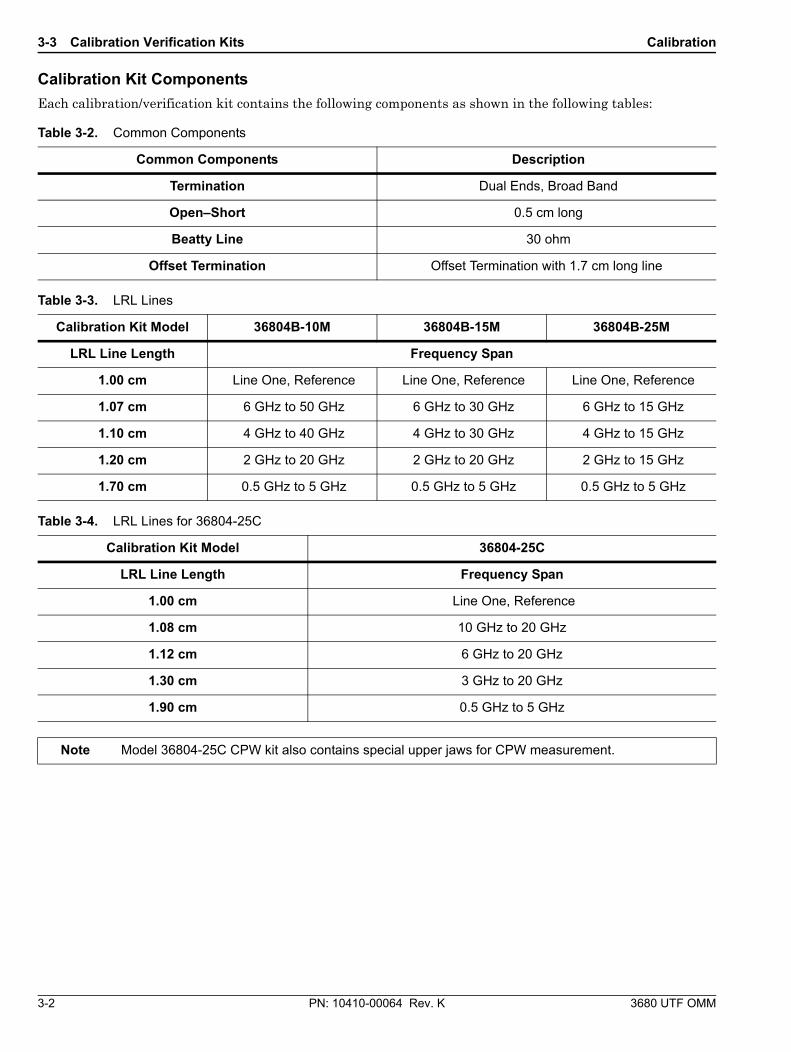
3-3 Calibration Verification Kits The UTF calibration/verification kits contain precision substrates of precisely known impedances for both OSL, LRL, and LRM calibrations. The kits also contain verification substrates for use in confirming the calibration accuracy. These verification substrates are a Beatty Line and an offset termination line. Table 3-1 shows the calibration/verification kits available for use with the UTF, their model numbers, substrate type, and frequency coverage. LRL lines provided represent physical length.
1. LRM Calibration Method of Rhode & Schwarz, Germany
Table 3-1. UTF Calibration/Verification Kits
Model Substrate Type Frequency
36804B-10M 10 mil (0.25 mm) Microstrip 0.04 GHz to 50 GHz
36804B-15M 15 mil (0.38 mm) Microstrip 0.04 GHz to 30 GHz
36804B-25M 25 mil (0.63 mm) Microstrip 0.04 GHz to 15 GHz
36804-25C 25 mil (0.63 mm) CPW 0.04 GHz to 20 GHz
3-3 Calibration Verification Kits Calibration
3-2 PN: 10410-00064 Rev. K 3680 UTF OMM
Calibration Kit Components
Each calibration/verification kit contains the following components as shown in the following tables:
Table 3-2. Common Components
Common Components Description
Termination Dual Ends, Broad Band
Open–Short 0.5 cm long
Beatty Line 30 ohm
Offset Termination Offset Termination with 1.7 cm long line
Table 3-3. LRL Lines
Calibration Kit Model 36804B-10M 36804B-15M 36804B-25M
LRL Line Length Frequency Span
1.00 cm Line One, Reference Line One, Reference Line One, Reference
1.07 cm 6 GHz to 50 GHz 6 GHz to 30 GHz 6 GHz to 15 GHz
1.10 cm 4 GHz to 40 GHz 4 GHz to 30 GHz 4 GHz to 15 GHz
1.20 cm 2 GHz to 20 GHz 2 GHz to 20 GHz 2 GHz to 15 GHz
1.70 cm 0.5 GHz to 5 GHz 0.5 GHz to 5 GHz 0.5 GHz to 5 GHz
Table 3-4. LRL Lines for 36804-25C
Calibration Kit Model 36804-25C
LRL Line Length Frequency Span
1.00 cm Line One, Reference
1.08 cm 10 GHz to 20 GHz
1.12 cm 6 GHz to 20 GHz
1.30 cm 3 GHz to 20 GHz
1.90 cm 0.5 GHz to 5 GHz
Note Model 36804-25C CPW kit also contains special upper jaws for CPW measurement.

Calibration 3-4 Calibration for Microstrip
3680 UTF OMM PN: 10410-00064 Rev. K 3-3
3-4 Calibration for Microstrip The following LRL, LRM, and OSL calibrations support Anritsu Model MS464xxx and 372xxx VNAs.
Line-Reflect-Line (LRL) Calibration
To perform an LRL calibration of the VNA for Microstrip:
1. Select the desired LRL line substrates from the appropriate microstrip calibration kit. When called for in the calibration sequence, mount the LRL line substrates on the UTF according to the “Substrate Mounting Procedure” in Section 2-3 of Chapter 2.
2. On the VNA:
a. Press the BEGIN CAL key.
b. Select CHANGE CAL METHOD AND LINE TYPE.
c. Select LRL/LRM and MICROSTRIP.
3. Continue through the calibration sequence selecting:
d. CALIBRATION TYPE
e. ISOLATION
f. DATA POINTS
g. FREQUENCY RANGE
When the CONFIRM CALIBRATION PARAMETERS menu is reached:
4. Select CHANGE MICROSTRIP PARAMETERS, then select the UTF calibration kit (10 MIL KIT, 15 MIL KIT, or 25 MIL KIT) from the menu.
5. Select CHANGE LRL/LRM PARAMETERS and select ONE BAND or TWO BANDS (refer to “Three-Line LRL Calibration and Combined LRL/LRM Calibration”).
6. Select CHANGE LRL/LRM PARAMETERS and select the LOCATION OF REFERENCE PLANES.
7. Select CHANGE LRL/LRM PARAMETERS and CHARACTERIZE CAL DEVICES:
a. For DEVICE 1, enter the length of LINE 1 (typically 1.00 cm).
b. For DEVICE 2, select LINE, then enter the length of the line (depends on the frequency range).
c. If TWO BANDS was selected in Step 5, for DEVICE 3, select LINE and enter the length of the line.
d. If TWO BANDS was selected in Step 5, then enter the BREAKPOINT frequency in GHz.
8. Select CHANGE LRL/LRM PARAMETERS, then NEXT CAL STEP and OFFSET LENGTH OF RELECTIVE DEVICE.
a. Enter OFFSET LENGTH (typically 0.0000 mm).
b. Select TYPE OF REFLECTION (typically LESS THAN Z0).
9. Select START CAL, then press ENTER.
10. Continue the calibration sequence, following the prompts. Mount the appropriate LRL line substrates when requested in the calibration sequence.
ISOLATION DEVICE is requested if ISOLATION was selected in the calibration sequence. This is usually a termination but in some applications, it is more convenient to use a reflection standard.
11. Store the calibration.
NoteThe user may use either the Open/Short Offset standard included in the calibration kit with the associated offset length of 0.5 cm or the jaws open or closed (short) with an offset length of 0.0000 mm. A short with the jaws closed is easiest to use and is therefore recommended.
3-4 Calibration for Microstrip Calibration
3-4 PN: 10410-00064 Rev. K 3680 UTF OMM
Line-Reflect-Match Calibration
LRM calibration is a variation of LRL calibration where a termination is substituted for line 2. LRM calibration can cover the same wide bandwidth as OSL calibration but LRM calibration results in a better source match.
To perform an LRM calibration of the VNA for Microstrip:
1. On the VNA press the BEGIN CAL key.
2. Select CHANGE CAL METHOD AND LINE TYPE.
3. Select LRL/LRM and MICROSTRIP.
4. Continue through the calibration sequence selecting:
a. CALIBRATION TYPE
b. ISOLATION
c. DATA POINTS
d. FREQUENCY RANGE
When the CONFIRM CALIBRATION PARAMETERS menu is reached:
5. Select CHANGE MICROSTRIP PARAMETERS, then select the UTF calibration kit (10 MIL KIT, 15 MIL KIT, or 25 MIL KIT) from the menu.
6. Select CHANGE LRL/LRM PARAMETERS and select ONE BAND or TWO BANDS (Refer to “Three-Line LRL Calibration and Combined LRL/LRM Calibration”).
7. Select CHANGE LRL/LRM PARAMETERS and select the LOCATION OF REFERENCE PLANES.
8. Select CHANGE LRL/LRM PARAMETERS and CHARACTERIZE CAL DEVICES.
a. For DEVICE 1, enter the length of LINE 1 as 1.00 cm.
b. For DEVICE 2, select MATCH.
c. If TWO BANDS was selected in Step 6 above, then for DEVICE 3, select LINE and enter the length of the line.
d. If TWO BANDS was selected in step Step 6 above, then enter the BREAKPOINT frequency in GHz.
e. Select CHANGE LRL/LRM PARAMETERS, then NEXT CAL STEP and OFFSET LENGTH OF REFLECTIVE DEVICE.
f. Enter OFFSET LENGTH (typically 0.000 mm). (Use the lower jaw of the UTF to short the connector.)
g. Select TYPE OF REFLECTION (typically LESS THAN Z0).
h. Select START CAL, then press ENTER.
9. Continue the calibration sequence, following the prompts.
Mount the appropriate line substrates when requested in the calibration sequence.
10. Store the calibration.
Note
The user may at his or her option use either the Open/Short Offset standard included in the calibration kit with the associated offset length of 0.5 cm or the jaws open or closed (short) with an offset length of 0.0000 mm. A short with the jaws closed is easiest to use and is therefore recommended.
NoteISOLATION DEVICE is requested if ISOLATION was selected in the calibration sequence. This is usually a termination; but, in some applications it is more convenient to use a reflection standard.
Calibration 3-4 Calibration for Microstrip
3680 UTF OMM PN: 10410-00064 Rev. K 3-5
Three-Line LRL Calibration and Combined LRL/LRM Calibration
Three-line LRL calibration is available for wide bandwidth application (> 10:1). Three-line LRL calibration allows concatenation of two LRL calibrations, or an LRL and an LRM calibration. The selection between two-line or three-line LRL calibrations is made from the CHANGE LRL/LRM PARAMETERS menu.
In general, the first line (Device 1) is always the 1.0 cm LRL line, the second line (Device 2) is the low frequency (long) LRL line (or the match for LRM), and the third line (Device 3) is the high frequency (short) LRL line.
For a combined LRL and LRM calibration, the second line (Device 2) is set to match and the dual termination is used instead of an LRL line. The three-line LRL calibration also asks for the breakpoint between the two calibrations.
For two LRL calibrations, select as breakpoint the upper frequency of the low frequency LRL line. For a combined LRL and LRM calibration, select as breakpoint the top frequency of the calibration divided by six. For example, to cover the frequency range 0.04 GHz to 40 GHz, select 6.7 GHz as the breakpoint.
Open-Short-Load Calibration
To perform an OSL calibration of the VNA for Microstrip:
1. Select the appropriate microstrip calibration kit. When called for in the calibration sequence, mount the appropriate substrate on the UTF according to the “Substrate Mounting Procedure” in Section 2-3 of Chapter 2.
2. On the VNA press BEGIN CAL key.
3. Select CHANGE CAL METHOD AND LINE TYPE.
4. Select STANDARD and MICROSTRIP.
5. Continue through the calibration sequence selecting:
a. CALIBRATION TYPE
b. ISOLATION
c. DATA POINTS
d. FREQUENCY RANGE
6. When the CONFIRM CALIBRATION PARAMETERS menu is reached:
a. Select CONNECTOR TYPE (one or two ports as required).
b. Select USER DEFINED and enter the coefficients supplied with the calibration kit. Be sure to enter the values for both the open and the short.
c. Select BROADBAND LOAD.
d. Select CHANGE MICROSTRIP PARAMETERS. Enter the appropriate microstrip parameters (listed in the calibration kit data). Press ENTER when complete.
e. Select START CAL, then press ENTER.
7. Continue the calibration sequence, following the prompts. Mount the appropriate calibration kit substrate when requested in the calibration sequence.
8. Store the calibration.
Recalibration with a Stored Calibration
When a new calibration is desired, recall the stored calibration, make any required minor changes, and recalibrate. All of the stored calibration coefficients will be in the new calibration.

3-5 Calibration for CPW Calibration
3-6 PN: 10410-00064 Rev. K 3680 UTF OMM
3-5 Calibration for CPW Before calibration of the VNA for CPW can begin, the microstrip upper jaws of the UTF must be replaced with the CPW jaws. The CPW upper jaws are included in the CPW calibration kit. After replacing the upper jaws of the UTF, adjust them using the adjustment procedure in Section 4-2 “Upper Jaw Adjustment”.
The VNA does not address measurement and calibration of CPW specifically. However, using microstrip parameters gives good results when the following guidelines are followed. The dimensions suggested below in Step 2 a and Step 2 b are smaller than the actual CPW calibration kit parameters. This compensates for the fact that CPW is much less dispersive than microstrip.
1. Follow the OSL or LRL calibration procedures in Section 3-4.
When the CONFIRM CALIBRATION PARAMETERS menu is reached:
2. Select CHANGE MICROSTRIP PARAMETERS, then select USER DEFINED.
The USER DEFINED MICROSTRIP PARAMETERS menu is then displayed. Enter the following parameters:
a. WIDTH OF STRIP: 0.2500 mm
b. THICKNESS OF SUBSTRATE: 0.2500 mm
c. ZC: 50.000
d. EFFECTIVE DIELECTRIC: 5.1
e. Press ENTER.
3. Continue the calibration sequence, following the procedures in Section 3-4 and the system prompts. Mount the appropriate substrate from the CPW calibration kit when requested in the calibration sequence.
4. Store the calibration.
Note The CPW upper jaws must be installed to the UTF connector blocks as shown in Figure 3-1.
Figure 3-1. CPW Jaw Installation
NoteThe CPW calibration kit is specified to 20 GHz. It can be used to 40 GHz, although special precautions may be necessary to prevent moding.
To UTF Block
To UTF Block
Calibration 3-6 Calibration Checks
3680 UTF OMM PN: 10410-00064 Rev. K 3-7
3-6 Calibration Checks There are three general techniques for checking the accuracy of a calibration:
• Measurement of calibration standards
• Measurement of known standards
• Measurement of assurance standards
The calibration kits contain components for all three techniques.
Measurement of Calibration Standards
The simplest, least accurate technique is to measure the calibration standards. This method is mainly a check of repeatability and is only as accurate as the calibration standards.
To perform calibration checks by measuring calibration standards:
1. After calibration, mount one of the calibration standards (an LRL line for LRL calibrations or a termination for OSL calibrations) on the UTF according to the “Substrate Mounting Procedure” in Section 2-3 of Chapter 2. Be sure to mount the substrate in the same orientation as during calibration.
2. On the VNA, measure S11 and S21. It will take some experience to determine how a good calibration looks. Experience can be gained by testing a number of calibrations using the the Measurement of Assurance Standards method and then noting the results obtained using Measurement of Calibration Standards method.
Measurement of Known Standards
This technique uses the Beatty Line as the known standard.
In theory, a 30 ohm Beatty Line standard gives a return loss of 6 dB and an insertion loss of 1.2 dB at each frequency that is an odd quarter wave multiple of its length and appears as a standard 50 ohm line at each frequency that is a half wave multiple of its length.
Microstrip is an imperfect medium for Beatty Line standards because it is lossy. The impedance changes with frequency and the low impedance line has a much lower cutoff frequency than the 50 ohm line. However, the results of measurements are very stable and the results of a good calibration will be repeatable.
To perform calibration checks by measuring a Beatty Line standard:
3. Mount the 1.7 cm line on the UTF according to the “Substrate Mounting Procedure” in Section 2-3.
4. On the VNA, store the S21 data of the 1.7 cm line to trace memory. Then use data divided by memory to subtract the loss of the line.
5. Remove the 1.7 cm line from the UTF. Then mount the Beatty Line standard on the UTF with the S21 display still showing data divided by memory so the loss of the 1.7 cm line is subtracted from the Beatty line.
6. On the VNA, measure S11 and S21.
a. For S11, the return loss should vary from approximately 7 dB to more than 20 dB. The depth of the nulls is a rough indication of the directivity.
b. For S21, the insertion loss should vary between approximately 0 dB and –1 dB and should be regular. The insertion loss values are not the theoretical 1.2 dB because of line losses.
NoteConsistent substrate mounting technique is very important for good results. Make sure that the substrate is resting against the dielectric spacers and the substrate is positioned so the contact pin is centered on the trace.
Note Variations from a smooth sine wave are indications of an imperfect calibration.

3-6 Calibration Checks Calibration
3-8 PN: 10410-00064 Rev. K 3680 UTF OMM
Measurement of Assurance Standards
This is the most accurate technique for evaluating the accuracy of a calibration. It uses independent assurance components to measure the directivity and source match values. Directivity measurements are made using the offset termination while source match measurements are made using the 1.70 cm line. The technique uses a length of transmission line to separate the error vector from the DUT vector allowing a direct measurement of directivity and source match.
To perform the source match assurance check:
1. Mount the 1.7 cm line on the UTF according to the “Substrate Mounting Procedure” in Section 2-3 of Chapter 2.
2. Connect the 1.7 cm line to one port of the UTF. Do not connect the other end.
3. On the VNA, observe S11 on a scale of approximately 1 dB. The open end of the line interacts with the source match to create a sine wave (ripple).
4. Measure the peak-to-peak amplitude of the ripple (source match error).
5. Convert the value of the source match error to dB using the RF Measurement Chart (Table 3-5 on page 3-9).
For example, if the ripples are 1 dB peak-to-peak the source match is 25 dB.
To perform the directivity assurance check, continue as follows:
6. Mount the offset termination on the UTF according to the “Substrate Mounting Procedure” in Section 2-3 of Chapter 2. Connect the offset termination to the test port.
7. On the VNA, observe S11. It should be a sine wave (ripple) centered approximately 20 dB down.
8. Measure both the average value of the ripple and the peak-to-peak amplitude of the ripple.
9. Convert the ripple peak-to-peak value to dB using the RF Measurement Chart (Table 3-5 on page 3-9). Add this value to the average value (dB down) of the ripple. This is the directivity.
For example, if the average value is 17 dB and the ripple is 2 dB peak-to-peak, the directivity is 17 dB + 19 dB = 36 dB.
Note
Source Match (SM) is defined here as the error due to a full reflection and is actually a combination of the True Source Match (TSM) and Directivity (D) errors according to the equation:
SM = D + TSM x (DUT)2
Thus the measured Source Match is the sum of the True Source Match and the Directivity.
NoteAssurance lines give direct indication of the errors due to source match and directivity; the ripples are the error window and the actual values are calculated using the RF Measurement Chart.
Note Irregularities in the display which are not part of the regular sine wave should be ignored.

Calibration 3-7 RF Measurement Chart
3680 UTF OMM PN: 10410-00064 Rev. K 3-9
3-7 RF Measurement ChartBelow are conversion tables for Return Loss, Reflection Coefficient, and SWR with tabular values for interaction of a small phasor x with a large phasor (unity reference) expressed in dB related to reference.
Table 3-5. RF Measurement Chart (1 of 2)
SWR Reflection Coefficient
Return Loss (dB)
Relative to Unity Reference
X dB Below Reference
REF + X (dB)
REF – X (dB)
REF ± X Peak to Peak Ripple (dB)
17.391 0.8913 1 1 5.535 –19.2715 24.8065
8.7242 0.7943 2 2 5.078 –13.7365 18.8145
5.848 0.7079 3 3 4.6495 –10.6907 15.3402
4.4194 0.631 4 4 4.2489 –8.6585 12.9073
3.5698 0.5623 5 5 3.8755 –7.1773 11.0528
3.0095 0.5012 6 6 3.5287 –6.0412 9.5699
2.6146 0.4467 7 7 3.2075 –5.1405 8.348
2.3229 0.3981 8 8 2.9108 –4.4096 7.3204
2.0999 0.3548 9 9 2.6376 –3.8063 6.4439
1.925 0.3162 10 10 2.3866 –3.3018 5.6884
1.7849 0.2818 11 11 2.1567 –2.8756 5.0322
1.6709 0.2512 12 12 1.9465 –2.5126 4.459
1.5769 0.2239 13 13 1.7547 –2.2013 3.9561
1.4935 0.1995 14 14 1.5802 –1.9331 3.5133
1.4326 0.1778 15 15 1.4216 –1.7007 3.1224
1.3767 0.1585 16 16 1.2778 –1.4988 2.7766
1.329 0.1413 17 17 1.1476 –1.3227 2.4703
1.288 0.1259 18 18 1.0299 –1.1687 2.1986
1.2528 0.1122 19 19 0.9237 –1.0337 1.9574
1.2222 0.1 20 20 0.8279 –0.9151 1.743
1.1957 0.0891 21 21 0.7416 –0.8108 1.5524
1.1726 0.0794 22 22 0.6639 –0.7189 1.3828
1.1524 0.0708 23 23 0.5941 –0.6378 1.2319
1.1347 0.0631 24 24 0.5314 –0.5661 1.0975
1.1192 0.0562 25 25 0.4752 –0.5027 0.9779
1.1055 0.0501 26 26 0.4248 –0.4466 0.8714
1.0935 0.0447 27 27 0.3796 –0.3969 0.7765
PHASORINTERACTION
X
(1 + X)
(REF)
(1 - X)
TERM002.DRW

3-7 RF Measurement Chart Calibration
3-10 PN: 10410-00064 Rev. K 3680 UTF OMM
1.0829 0.0398 28 28 0.3391 –0.3529 0.6919
1.0736 0.0355 29 29 0.3028 –0.3138 0.6166
1.0653 0.0316 30 30 0.2704 –0.2791 0.5495
1.058 0.0282 31 31 0.2414 –0.2483 0.4897
1.0515 0.0251 32 32 0.2155 –0.2210 0.4365
1.0458 0.0224 33 33 0.1923 –0.1967 0.389
1.0407 0.02 34 34 0.1716 –0.1751 0.3467
1.0362 0.0178 35 35 0.1531 –0.1558 0.309
1.0322 0.0158 36 36 0.1366 –0.1388 0.2753
1.0287 0.0141 37 37 0.1218 –0.1236 0.2454
1.0255 0.0126 38 38 0.1087 –0.1100 0.2187
1.0227 0.0112 39 39 0.0969 –0.0980 0.1949
1.0202 0.01 40 40 0.0864 –0.0873 0.1737
1.018 0.0089 41 41 0.0771 –0.0778 0.1548
1.016 0.0079 42 42 0.0687 –0.0693 0.138
1.0143 0.0071 43 43 0.0613 –0.0617 0.123
1.0127 0.0063 44 44 0.0546 –0.0550 0.1096
1.0113 0.0056 45 45 0.0487 –0.0490 0.0977
1.0101 0.005 46 46 0.0434 –0.0436 0.0871
1.009 0.0045 47 47 0.0387 –0.0389 0.0776
1.008 0.004 48 48 0.0345 –0.0346 0.0692
1.0071 0.0035 49 49 0.0308 –0.0309 0.0616
1.0063 0.0032 50 50 0.0274 –0.0275 0.0549
1.0057 0.0028 51 51 0.0244 –0.0245 0.049
1.005 0.0025 52 52 0.0218 –0.0218 0.0436
1.0045 0.0022 53 53 0.0194 –0.0195 0.0389
1.004 0.002 54 54 0.0173 –0.0173 0.0347
1.0036 0.0018 55 55 0.0154 –0.0155 0.0309
1.0032 0.0016 56 56 0.0138 –0.0138 0.0275
1.0028 0.0014 57 57 0.0123 –0.0123 0.0245
1.0025 0.0013 58 58 0.0109 –0.0109 0.0219
1.0022 0.0011 59 59 0.0097 –0.0098 0.0195
1.002 0.001 60 60 0.0087 –0.0087 0.0174
Table 3-5. RF Measurement Chart (2 of 2)
SWR Reflection Coefficient
Return Loss (dB)
Relative to Unity Reference
X dB Below Reference
REF + X (dB)
REF – X (dB)
REF ± X Peak to Peak Ripple (dB)
PHASORINTERACTION
X
(1 + X)
(REF)
(1 - X)
TERM002.DRW
3680 UTF OMM PN: 10410-00064 Rev. K 4-1
Chapter 4 — Maintenance
4-1 Introduction This section provides instructions for maintaining the UTF. Maintenance is limited to adjustment of the connector block upper jaws, removal and replacement of connectors, and preventive maintenance.
4-2 Upper Jaw Adjustment The adjustment of the connector block upper jaws is critical to correct operation of the UTF. The upper jaw must be the exact distance above the center conductor pin to ensure the proper pin-to-substrate pressure contact. In addition, the upper jaws must be exactly parallel to each other for correct clamping action.
Jaw Types
There are two types of connector block upper jaws; one for microstrip and one for CPW. The microstrip upper jaw has two different connector configurations; a semicircle and a slot. The semicircle configuration is used for most applications. The slot configuration is used when making measurements of very narrow microstrip, but will degrade the scalar performance. The narrow slot configuration may also be used for CPW connection but adjusting planarity is difficult.
The CPW upper jaws come as part of the CPW calibration kit. The CPW upper jaws have spring contact fingers for good ground connection. The jaws have two different spring spacing widths; 0.032 in. and 0.040 in. Choose the spring spacing width that best fits the CPW being tested. The spring spacing for the standard CPW calibration kit is 0.032 in.
Adjustment Block
The UTF comes with an adjustment block that allows precise alignment of the upper jaws. The thickness of the adjustment block has been set for the UTF associated with it.
Required Tools
• Screwdriver, Phillips
Adjustment Steps
1. Hold the lower jaw open during the adjustment Press the lever to open the jaw and then place a suitable object (such as a wood cotton swab stick) between the back side of the lever and the housing to keep the jaw from closing as the lever is released.
2. Chose the desired upper jaw configuration and mount in the UTF.
3. Loosely tighten the upper jaw screws, grasping and turning the screwdriver by its shaft to apply the tightening torque.
4. Place the adjustment block under the jaw at an angle.
5. Press the block down onto the rods levering the jaw upwards.
When the block is sitting on the rods, the lower surface of the jaw should press evenly and snugly against it.
CautionDo not remove the tape on the bottom of the adjustment block. The tape is used to shim the block to the exact dimension required by the UTF associated with it.

4-3 Connector Removal and Replacement Maintenance
4-2 PN: 10410-00064 Rev. K 3680 UTF OMM
6. Tighten the upper jaw screws firmly. Do not over torque.
7. Inspect for proper connector pin movement per the instructions in Section 4-3, “Connector Installation”, Step 8.
8. Repeat Step 1 through Step 7 for the other upper jaw if needed.
4-3 Connector Removal and Replacement The connector is easily removed for cleaning and replacement. The most critical part of the connector is the small pin that contacts the substrate. It must be kept clean and accurately positioned. Refer to Section 4-4 for routine cleaning instructions. If the pin becomes bent, broken, or very dirty, the connector must be removed to make the necessary repairs.
Required Tools
• Wrenches, 5/16 in, 2 each
• Connector removal tools, barrel and stop
• Torque wrench, 8 inch/pounds
Connector Removal
1. Hold the UTF jaws open by placing the thin sheet metal jaw separator between the upper and lower jaws.
2. Set the gap between the connector removal tool barrel and the stop to approximately 1/16 inch.
3. Screw the connector removal tool onto the connector and tighten it hand tight.
4. Place the wrenches on the connector removal tool barrel and the stop. Set the angle between them at approximately 45 degrees.
5. Squeeze the wrenches together firmly, using one hand. This is important to prevent torquing the housing of the UTF.
6. Use a wrench on the barrel to remove the connector. If the removal tool loosens, repeat the above step but squeeze the wrenches more firmly.
7. Repair or replace the connector as required. When replacing the connector or connector pin, use the following Anritsu parts:
• 3.5 mm and K Connector Pin – P/N B22849
• V Connector Pin – P/N B22490
• K Connector – P/N B22845
• V Connector – P/N B22848
• 3.5 mm Connector – P/N B22846
CautionWhen removing or replacing a connector always keep the UTF jaws open. Failure to do so can result in damage to the connector pin.
Note
The UTF comes with a thin sheet metal jaw separator installed between the upper and lower jaws. This relieves the pressure on the connector pin. It is good practice to install the separator whenever the UTF will not be used for a long period of time or is placed in storage. When installing the jaw separator, position it off center so that it does not contact the connector pin.
NoteThe center conductor assembly can be removed from the outer conductor without removing the outer conductor from the connector removal tool.
Maintenance 4-4 Preventive Maintenance
3680 UTF OMM PN: 10410-00064 Rev. K 4-3
Connector Installation
1. Ensure that the UTF jaws are still held open.
2. Ensure that the outer conductor is still locked into the connector removal tool.
3. Install the center conductor assembly into the outer conductor.
4. Screw the connector hand tight into the UTF.
5. View the position of the pin in the hole of the connector block.
The pin must be either centered or below center toward the lower jaw. The maximum that the pin can be off center is 1/3 the diameter of the pin. If it is off center by more than the maximum, the connector must be replaced. If the pin is off center by less than the maximum but its location is not toward the lower jaw, it must be adjusted.
a. To adjust, note the pin’s off center position, then remove the connector from the UTF.
b. Use a probe to rotate the center conductor assembly to the correct position and then reinstall the connector in the UTF.
6. Torque the connector to 8 inch/pounds.
7. Reinspect the pin for proper positioning. Adjust as required by repeating the above steps.
8. Insert a substrate into the UTF and test for correct pin-to-substrate contact by permitting the lower jaw to close while observing the pin.
The pin should deflect a minimum of 1/3 its diameter and still be centered in the hole within 1/3 of its diameter. If this is not the case, the connector block upper jaw must be adjusted, refer to Section 4-2 for instructions.
4-4 Preventive Maintenance The following preventive maintenance is recommended for the UTF:
UTF Maintenance
1. Keep the areas in the vicinity of the substrate clean and free of material. Use a cotton swab, dampened with isopropyl alcohol, to clean these areas. Be careful not to distort the pin. Open the lower jaw while cleaning.
2. Keep the slide rods free of dirt. Clean them with an isopropyl alcohol dampened wipe.
Calibration Kit Maintenance
1. Keep the calibration substrates in the holder except when in use.
2. Always handle the calibration substrates by the side edges. Avoid touching the ends.
3. If the components of the calibration kits require cleaning, use a swab dampened with isopropyl alcohol.
NoteBe sure to reuse any tuning shim(s) which are on the small pin and any pin depth shim(s) which are between the center conductor and outer conductor.
CautionWhen replacing a connector on the UTF, do not over torque the connector. Over torquing can result in damage to the UTF.

4-4 Preventive Maintenance Maintenance
4-4 PN: 10410-00064 Rev. K 3680 UTF OMM
3680 UTF OMM PN: 10410-00064 Rev. K 5-1
Chapter 5 — Using Optional Accessories
5-1 IntroductionThe UTF optional accessories are the Model 36801 Right Angle Launcher, the Model 36802 MMIC Attachment, and the Model 36803 Bias Probe. This chapter contains a brief description of each accessory, procedures for mounting it on the UTF, and its individual operational requirements.
5-2 Right-Angle Launcher
General Information
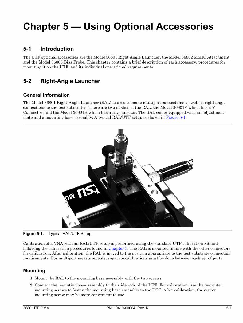
The Model 36801 Right-Angle Launcher (RAL) is used to make multiport connections as well as right angle connections to the test substrates. There are two models of the RAL; the Model 36801V which has a V Connector, and the Model 36801K which has a K Connector. The RAL comes equipped with an adjustment plate and a mounting base assembly. A typical RAL/UTF setup is shown in Figure 5-1.
Calibration of a VNA with an RAL/UTF setup is performed using the standard UTF calibration kit and following the calibration procedures found in Chapter 3. The RAL is mounted in line with the other connectors for calibration. After calibration, the RAL is moved to the position appropriate to the test substrate connection requirements. For multiport measurements, separate calibrations must be done between each set of ports.
Mounting
1. Mount the RAL to the mounting base assembly with the two screws.
2. Connect the mounting base assembly to the slide rods of the UTF. For calibration, use the two outer mounting screws to fasten the mounting base assembly to the UTF. After calibration, the center mounting screw may be more convenient to use.
Figure 5-1. Typical RAL/UTF Setup
5-2 Right-Angle Launcher Using Optional Accessories
5-2 PN: 10410-00064 Rev. K 3680 UTF OMM
3. For calibration, mount the RAL in line with and facing the sliding connector block of the UTF. Position the RAL as close to the fixed connector block as possible.
Calibration
1. Mount and connect the RAL in line with and facing the sliding connector as described in the mounting instructions above.
2. Calibrate the VNA with the UTF in the normal manner following the calibration procedures in Chapter 3. Store the calibration data.
Measurement Setup
1. After calibration, loosen or remove the RF cable from the RAL.
2. Move the RAL to the appropriate location on the UTF, leaving the mounting screws for both the mounting base assembly and the RAL slightly loose.
3. Mount the substrate to be tested into the jaws of the sliding connector block and if appropriate, the fixed connector block.
4. Carefully adjust the position of the RAL so that the desired trace on the substrate is directly below the RAL center pin and is contacting the dielectric spacer rods.
5. Tighten the mounting screws.
6. Connect the RF cable, recall the appropriate calibration data, and make the test substrate measurements.
Upper Jaw Adjustment (if Required)
1. Clamp the one inch square adjustment plate supplied with the RAL into the UTF jaws.
2. Adjust the set screw in the lever of the RAL so that it opens the lower jaw. This prevents damage to the connector pin.
3. Loosen the RAL upper jaw screws.
4. Position the RAL so that the adjustment plate is under the upper jaw.
5. While applying slight pressure to the upper jaw, tighten the upper jaw screws firmly. Do not over torque.
6. Readjust the set screw in the lever of the RAL so that the lower jaw closes fully.
7. Inspect for the correct connector pin-to-substrate contact as described in Chapter 4, Section 4-3, “Connector Installation”.
Multiport Measurements
A separate calibration is required for each pair of test ports. Insure that the proper calibrations are stored on the disk so that they can be recalled when needed. Mount the substrate to be tested into the UTF and recall the desired calibration. It is important to remember that unused ports are not calibrated and therefore are not well terminated. If well matched loads are required, it is recommended that the port be padded with a 6 dB or 10 dB attenuator.
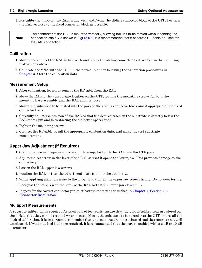
NoteThe connector of the RAL is mounted vertically, allowing the unit to be moved without bending the connection cable. As shown in Figure 5-1, it is recommended that a separate RF cable be used for the RAL connection.
Using Optional Accessories 5-3 MMIC Attachment
3680 UTF OMM PN: 10410-00064 Rev. K 5-3
5-3 MMIC Attachment
General Information
The Model 36802 MMIC Attachment is used to support testing of small substrates or substrates where it is not feasible to make connections with the UTF jaws. The MMIC attachment consists of two cam driven connection pin assemblies and a mounting base assembly. A connection substrate kit, which must be ordered separately, contains four connection substrates, a carrier mounting block, two shorts, and a spare pin foot. There are three models of the connection substrate kit; Model 36805-10M which supports testing of 10 mil substrates, Model 36805-15M which supports testing of 15 mil substrates, and Model 36805-25M which supports testing of 25 mil substrates.
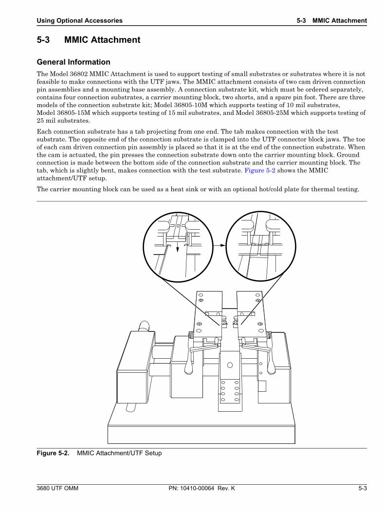
Each connection substrate has a tab projecting from one end. The tab makes connection with the test substrate. The opposite end of the connection substrate is clamped into the UTF connector block jaws. The toe of each cam driven connection pin assembly is placed so that it is at the end of the connection substrate. When the cam is actuated, the pin presses the connection substrate down onto the carrier mounting block. Ground connection is made between the bottom side of the connection substrate and the carrier mounting block. The tab, which is slightly bent, makes connection with the test substrate. Figure 5-2 shows the MMIC attachment/UTF setup.
The carrier mounting block can be used as a heat sink or with an optional hot/cold plate for thermal testing.
Figure 5-2. MMIC Attachment/UTF Setup

5-3 MMIC Attachment Using Optional Accessories
5-4 PN: 10410-00064 Rev. K 3680 UTF OMM
Calibration of the VNA with the MMIC attachment/UTF setup consists of an LRL calibration using the standard UTF calibration kit and the Chapter 3 calibration procedures. High frequency calibrations, at 4 GHz are performed on the carrier mounting block and include the effects of the tab-to-substrate bond. Low frequency calibrations less than 4 GHz are done before mounting the MMIC attachment to the UTF.
Mounting
To mount the MMIC attachment to the UTF, proceed as follows:
1. Attach the MMIC mounting base assembly to the UTF slide rods using the center screw. (The MMIC carrier mounting block is held by the mounting base assembly.)
Tighten the screw just enough to allow the unit to slide; rotating the rectangular block slightly with a finger will loosen and tighten the base.
2. Mount the connection substrates into the jaws of the fixed and sliding connector blocks of the UTF.
Insure that they are correctly positioned and firmly pressed against the dielectric spacer rods.
3. Move the UTF’s sliding connector block to position the substrate tabs close to each other but not touching.
Insure that the tabs are in line. If they are not in line, adjust the offset block of the UTF until they are in line.
4. Slide a carrier mounting block into the mounting base assembly.
The top of the block should be approximately 5 to 9 mils below the bottom of the connection substrates.
This gap can be enlarged by holding the connection substrate slightly above its natural position while clamping it into the UTF jaws. The gap can be narrowed by placing tape on the bottom of the carrier block.
5. Slide the MMIC mounting base assembly so that the connection substrate locked into the jaws of the fixed connector block overlaps the carrier block by approximately 0.030 inch.
6. Set a test substrate onto the carrier block and slide it under the tab of the connection substrate locked into the jaws of the fixed connector block. Use care to avoid damaging the tab. The test substrate height may need to be readjusted.
7. Move the sliding connector block until the test substrate is almost clamped between the two connection substrates. This will help to protect the tabs while the cam assemblies are being installed.
8. Install the cam assemblies, insuring that the cams are set so that the pins are in the upper most position (lever up). Use care to avoid damaging the connection substrate tabs.
9. Adjust each cam assembly so that the toe of the pin is directly centered over the tab and just touches the end of the connection substrate. Tighten the screws holding the cam assemblies.
10. Inspect the MMIC attachment/UTF setup to insure the following:
• The connection substrate tabs are in line over the test substrate.
• The cam assembly pins are properly placed over the tabs and the toe of each pin does not extend past the connection substrate.
• The connection substrate ends are parallel so that the test substrate is held properly.
Caution Use care when handling the connection substrates to avoid damaging the tabs.
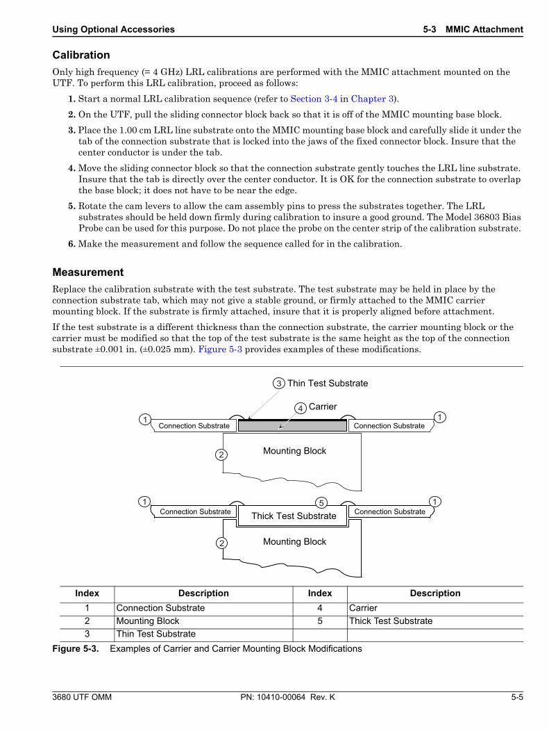
Using Optional Accessories 5-3 MMIC Attachment
3680 UTF OMM PN: 10410-00064 Rev. K 5-5
Calibration
Only high frequency (= 4 GHz) LRL calibrations are performed with the MMIC attachment mounted on the UTF. To perform this LRL calibration, proceed as follows:
1. Start a normal LRL calibration sequence (refer to Section 3-4 in Chapter 3).
2. On the UTF, pull the sliding connector block back so that it is off of the MMIC mounting base block.
3. Place the 1.00 cm LRL line substrate onto the MMIC mounting base block and carefully slide it under the tab of the connection substrate that is locked into the jaws of the fixed connector block. Insure that the center conductor is under the tab.
4. Move the sliding connector block so that the connection substrate gently touches the LRL line substrate. Insure that the tab is directly over the center conductor. It is OK for the connection substrate to overlap the base block; it does not have to be near the edge.
5. Rotate the cam levers to allow the cam assembly pins to press the substrates together. The LRL substrates should be held down firmly during calibration to insure a good ground. The Model 36803 Bias Probe can be used for this purpose. Do not place the probe on the center strip of the calibration substrate.
6. Make the measurement and follow the sequence called for in the calibration.
Measurement
Replace the calibration substrate with the test substrate. The test substrate may be held in place by the connection substrate tab, which may not give a stable ground, or firmly attached to the MMIC carrier mounting block. If the substrate is firmly attached, insure that it is properly aligned before attachment.
If the test substrate is a different thickness than the connection substrate, the carrier mounting block or the carrier must be modified so that the top of the test substrate is the same height as the top of the connection substrate ±0.001 in. (±0.025 mm). Figure 5-3 provides examples of these modifications.
Index Description Index Description
1 Connection Substrate 4 Carrier
2 Mounting Block 5 Thick Test Substrate
3 Thin Test Substrate
Figure 5-3. Examples of Carrier and Carrier Mounting Block Modifications
Mounting Block
Thick Test Substrate1 1
2
5Connection SubstrateConnection Substrate
Mounting Block
Thin Test Substrate
Carrier
Connection Substrate1 1
2
3
4
Connection Substrate
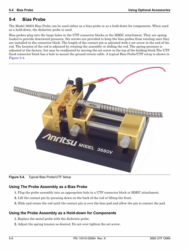
5-4 Bias Probe Using Optional Accessories
5-6 PN: 10410-00064 Rev. K 3680 UTF OMM
5-4 Bias Probe The Model 36803 Bias Probe can be used either as a bias probe or as a hold-down for components. When used as a hold-down, the dielectric probe is used.
Bias probes plug into the large holes in the UTF connector blocks or the MMIC attachment. They are spring loaded to provide downward pressure. Set screws are provided to keep the bias probes from rotating once they are installed in the connector block. The length of the contact pin is adjusted with a set screw in the end of the rod. The location of the rod is adjusted by rotating the assembly or sliding the rod. The spring pressure is adjusted at the factory, but may be readjusted by moving the set screw in the top of the holding block.The UTF fixed connector block has a hole to mount the ground return cable. A typical Bias Probe/UTF setup is shown in Figure 5-4.
Using The Probe Assembly as a Bias Probe
1. Plug the probe assembly into an appropriate hole in a UTF connector block or MMIC attachment.
2. Lift the contact pin by pressing down on the back of the rod or lifting the front.
3. Slide and rotate the rod until the contact pin is over the bias pad and allow the pin to contact the pad.
Using the Probe Assembly as a Hold-down for Components
1. Replace the metal probe with the dielectric probe.
2. Adjust the spring tension as desired. Do not over tighten the set screw.
Figure 5-4. Typical Bias Probe/UTF Setup

3680 UTF OMM PN: 10410-00064 Rev. K 6-1
Chapter 6 — Applications
6-1 IntroductionThis chapter provides additional information on subjects related to the UTF. Information is provided concerning:
• UTF-to-microstrip connection pin design.
• Upper jaw modification.
• Making LRL calibration lines.
• Measurement considerations for soft substrate, substrate on a carrier, and substrate of different thickness than the calibration substrate.
• Substrate moding.
6-2 UTF-to-Microstrip Connection Pin Design The center conductor pin on the back side of the UTF’s RF connector (a K Connector or a V Connector) makes spring-loaded pressure contact with the microstrip. The center conductor pins of the K Connector and the V Connector differ in design. As illustrated in Figure 6-1, the main design difference between the two is that the pin of the K Connector contacts the substrate about 4 mils (0.1 mm) in from the edge of the substrate, while the pin of the V Connector must make contact at the edge of the substrate. The reason for this is that some design criteria demands that the microstrip trace end before the edge of the substrate. In such cases, a straight pin may not make contact with such a trace. At 60 GHz; however, not making contact at the edge results in poor RF performance.
Index Description
1 K Connector Pin (P/N B22849)
2 V Connector Pin (P/N B22490)
3 Substrate
Figure 6-1. UTF-to-Microstrip Connection Pins
K Connector Pin(P/N B22849)
V Connector Pin(P/N B22490)
Substrate
Substrate
1
2
3
3

6-3 Upper Jaw Modification Applications
6-2 PN: 10410-00064 Rev. K 3680 UTF OMM
6-3 Upper Jaw Modification The connector block upper jaw of the UTF can be modified to allow correct connection pin-to-substrate contact when the substrate is mounted in a channel on a carrier. Behind the upper jaw on the connector block are alternate mounting holes. The location of these alternate mounting holes in relation to the standard upper jaw mounting holes are shown in Figure 6-2 and are identified by the dashed circles labeled ALT. The alternate holes can be used if the standard screw location is in the way of proper connection. An example of upper jaw modification is shown in the lower half of Figure 6-2. A kit of upper jaws is available. Order Anritsu P/N C23845.
Index Description
1 Slot for Narrow Substrates
2 ALT (Alternate)
3 STD (Standard)
4 Stardard Upper Jaw
5 Modified Upper Jaw
6 Non-Standard Hole
7 Cutout
Figure 6-2. UTF Upper Jaws, Standard and Modified
.150
.300 STD
.500
Non-Standard Hole Cutout
Slot for Narrow Substrates
Standard Upper Jaw
Modified Upper Jaw
ALT
ALTALTALTALT STD STD
1
2 2 2 233
4
6
5
7
Applications 6-4 Making LRL Calibration Lines
3680 UTF OMM PN: 10410-00064 Rev. K 6-3
6-4 Making LRL Calibration Lines LRL calibration lines can be easily made from Microstrip using the following steps. Although it is not critical that the characteristic impedance of the LRL lines be exactly 50 ohms, for correct dispersion compensation the impedance should be within the range of 45 to 55 ohms.
1. Decide on frequency span. The maximum span is 9:1.
2. Select length of line one. 1 cm is a good choice.
3. Calculate the length of line 2. This length is 1/4 wavelength longer than line 1 at the center frequency. The center frequency is (F1 + F2)/2. Be sure to take the dielectric constant into account.
4. Make lengths of your transmission line.
6-5 Measurement Considerations
Soft Substrate
When making measurements of soft substrate, the substrate lines should be at least 1 cm wide to prevent the soft material from being crushed by the pressure of the UTF jaws.
If the VNA is calibrated using an alumina calibration kit, then there will be some errors involved when making soft substrate measurements. The first measurement error is the interface connection mismatch caused by the change in substrates. This error is approximately 33 dB per connection at 20 GHz and 27 dB per connection at 40 GHz. The second measurement error is due to the change in dielectric constant which results in poor measurement phase accuracy. The amplitude accuracy of the measurements will be only slightly degraded. If desired, LRL calibration lines of soft substrate can easily be made.
Substrate on Carriers
Measurements of substrate on carriers can be made, but if the VNA is calibrated using a standard calibration kit, there will be an interface connection mismatch. This interface connection mismatch is proportional to the thickness of the carrier and is caused by the inductive effect of the longer ground path. The mismatch error from a 30 mil carrier at 20 GHz is approximately 30 dB per connection. Very thick carriers are not recommended, especially at frequencies above 20 GHz. If desired, LRL calibration lines of substrate on carrier can be made.
It is extremely important that the carriers be flat. If they have a concave bow, the ground connection will not be made directly under the connector pin and poor measurement results can be expected.
On some carriers, the substrate sits in a channel, with the top of the carrier extending above the top of the substrate. In this case, the upper jaw of the UTF will prevent the substrate from making contact with the connection pin. The upper jaw can be modified to allow correct connection pin-to-substrate contact (paragraph 6-3).
Substrate of Different Thickness than the Calibration Substrate
When making measurements of a test substrate that has a different thickness than the calibration substrate, there are two measurement errors involved. These measurement errors are:
• An interface connection mismatch error and
• A phase accuracy error due to the different dispersion characteristics of the substrates.
NoteIf the substrate used has a low dielectric constant, there could be some moding. Refer to Section 6-6 for more on substrate moding.

6-6 Substrate Moding Applications
6-4 PN: 10410-00064 Rev. K 3680 UTF OMM
The interface connection mismatch error will be proportional to the difference between the substrates. For example, if the calibration substrate is 10 mil alumina and the test substrate is 15 mil alumina, the interface error at 20 GHz is approximately 32 dB at each connection. Section 6-5 provides more information on interface connection mismatches.
6-6 Substrate Moding On the UTF, substrate ground is made only at the connection ends of the substrate. This does not pose a problem in most cases, especially if the substrate has a high dielectric constant. But if the substrate has a low dielectric constant, such as RT/duroid ® or quartz, there may be some moding or glitches at various frequencies. This is due to secondary modes which can reach the edge boundaries and become resonant. The resonant frequencies are proportional to the width of the substrate. In most cases, these resonances can be damped by simply placing an absorber type material (such as Eccosorb™) near the edges of the substrate. In extreme cases, the edges of the substrate must be metalized. The lossy material used normally causes no additional loss to the main mode.
Numerics to U
3680 UTF OMM PN: 10410-00064 Rev. K Index-1
IndexNumerics
3680 UTF description . . . . . . . . . . . . . . . . . . . 1-1, 1-3
Aalignment block . . . . . . . . . . . . . . . . . . . . . . . . . . 1-4
Bbias probe . . . . . . . . . . . . . . . . . . . . . . . . . . . . . . . 5-6
Ccal kit maintenance . . . . . . . . . . . . . . . . . . . . . . . 4-3calibration
combined LRL/LRM calibration . . . . . . . . . . 3-5CPW . . . . . . . . . . . . . . . . . . . . . . . . . . . . . . . . 3-6LRL . . . . . . . . . . . . . . . . . . . . . . . . . . . . . . . . . 3-1LRM . . . . . . . . . . . . . . . . . . . . . . . . . . . . . . . . 3-1methods . . . . . . . . . . . . . . . . . . . . . . . . . . . . . 3-1three line . . . . . . . . . . . . . . . . . . . . . . . . . . . . . 3-5verification kits . . . . . . . . . . . . . . . . . . . . . . . 3-1VNA calibrations . . . . . . . . . . . . . . . . . . . . . . 3-1
carrier mounted substrates . . . . . . . . . . . . . . . . . 2-5connector
installation . . . . . . . . . . . . . . . . . . . . . . . . . . . 4-3removal . . . . . . . . . . . . . . . . . . . . . . . . . . . . . . 4-2
conversion tables . . . . . . . . . . . . . . . . . . . . . . . . . 3-9coplanar waveguide, considerations . . . . . . . . . . 2-5CPW . . . . . . . . . . . . . . . . . . . . . . . . . . . . . . . . . . . . 1-1
Ddielectric spacer rods . . . . . . . . . . . . . . . . . . . . . . 1-4
Ffixed connector block . . . . . . . . . . . . . . . . . . . . . . 1-4fixed upper jaw . . . . . . . . . . . . . . . . . . . . . . . . . . . 1-4frequency range . . . . . . . . . . . . . . . . . . . . . . . . . . 1-1
Jjaw
adjustment . . . . . . . . . . . . . . . . . . . . . . . . . . . 4-1description . . . . . . . . . . . . . . . . . . . . . . . . . . . 1-4modification . . . . . . . . . . . . . . . . . . . . . . . . . . 6-2
Llever . . . . . . . . . . . . . . . . . . . . . . . . . . . . . . . . . . . . 1-3line-reflect-line calibration . . . . . . . . . . . . . . . . . . 3-3line-reflect-match calibration . . . . . . . . . . . . . . . . 3-4
Mmaintenance
UTF . . . . . . . . . . . . . . . . . . . . . . . . . . . . . . . . . 4-3making LRL cal lines . . . . . . . . . . . . . . . . . . . . . . 6-3measurement
assurance standards . . . . . . . . . . . . . . . . . . . 3-8calibration standards . . . . . . . . . . . . . . . . . . . 3-7known standards . . . . . . . . . . . . . . . . . . . . . . 3-7
measurement considerationssoft substrate . . . . . . . . . . . . . . . . . . . . . . . . . .6-3substrate moding . . . . . . . . . . . . . . . . . . . . . . .6-4substrate on carrier . . . . . . . . . . . . . . . . . . . . .6-3substrate thickness . . . . . . . . . . . . . . . . . . . . .6-3
MMIC attachment . . . . . . . . . . . . . . . . . . . . . . . . .5-3model 36805 substrate kits . . . . . . . . . . . . . . . . . .1-2movable lower jaw . . . . . . . . . . . . . . . . . . . . . . . . .1-4
Ooffset block . . . . . . . . . . . . . . . . . . . . . . . . . . . . . . .1-4operating with
scalar network analyzer system . . . . . . . . . . .2-1VNA system . . . . . . . . . . . . . . . . . . . . . . . . . . .2-3
optional accessoriesmodel 36801 right angle launcher . . . . . . . . .1-1model 36802 MMIC attachment . . . . . . . . . . .1-2model 36803 bias probe . . . . . . . . . . . . . . . . . .1-2
OSL calibration . . . . . . . . . . . . . . . . . . . . . . . . . . .3-1
Pphasor interaction . . . . . . . . . . . . . . . . . . . . . . . . .3-9pin design . . . . . . . . . . . . . . . . . . . . . . . . . . . . . . . .6-1probe
bias . . . . . . . . . . . . . . . . . . . . . . . . . . . . . . . . . .5-6hold-down . . . . . . . . . . . . . . . . . . . . . . . . . . . . .5-6
RRAL . . . . . . . . . . . . . . . . . . . . . . . . . . . . . . . . . . . . .5-1RF measurement chart . . . . . . . . . . . . . . . . . . . . .3-9right angle launcher . . . . . . . . . . . . . . . . . . . . . . . .5-1
Ssafety symbols
for safety . . . . . . . . . . . . . . . . . . . . . . . . . Safety-2in manuals . . . . . . . . . . . . . . . . . . . . . . . Safety-1on equipment . . . . . . . . . . . . . . . . . . . . . Safety-1
slide rods . . . . . . . . . . . . . . . . . . . . . . . . . . . . . . . . .1-4sliding connector block . . . . . . . . . . . . . . . . . . . . . .1-4small phasor-large phasor interaction . . . . . . . . .3-9substrate moding . . . . . . . . . . . . . . . . . . . . . . . . . .6-4substrate stop . . . . . . . . . . . . . . . . . . . . . . . . . 1-3, 2-5
Tthree line calibration . . . . . . . . . . . . . . . . . . . . . . .3-5
UUTF
components . . . . . . . . . . . . . . . . . . . . . . . . . . . .1-3description . . . . . . . . . . . . . . . . . . . . . . . . . . . .1-1frequency ranges . . . . . . . . . . . . . . . . . . . . . . .1-1maintenance . . . . . . . . . . . . . . . . . . . . . . . . . . .4-3models . . . . . . . . . . . . . . . . . . . . . . . . . . . . . . . .1-1

Anritsu prints on recycled paper with vegetable soybean oil ink.
Anritsu Company490 Jarvis Drive
Morgan Hill, CA 95037-2809USA