39. radiation and devices – part i
TRANSCRIPT

130
130
39. RADIATION AND DEVICES – PART I
39.1 Review/Background:
Memory plays a very critical role in determining the performance of a system.
Starting from the 70s, memory technologies such as DRAM have undergone a steady
increase in data retention time and the data access rates (Figure. 39.1). However in the
near future, serious scaling challenges lie ahead for processing of DRAM cells.
Figure. 39.1. Evolution trend for DRAM

131
131
39.2 1Transistor-1Capacitor (1T-1C) Cell
Figure. 39.2 shows a typical 1T-1C DRAM cell. Data is represented by the
charge stored on the capacitor which is the dominant area-consuming part of the cell.
Writing into the DRAM cell involves charging and discharging of this capacitor. Due to
parasitic leakage paths, the charge on the capacitor is gradually lost and hence the DRAM
cell needs to be refreshed periodically.
A smaller capacitor is desirable since it would involve fewer charges being
stored or removed. However, the capacitor and hence the cell cannot be made arbitrarily
small since a very small capacitor cannot hold enough charge. This imposes serious
limitations on DRAM scaling.
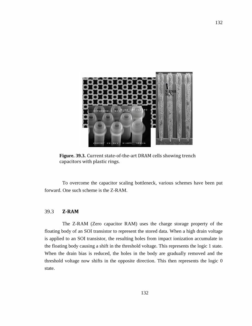
The state-of-the-art DRAM has capacitors fabricated in the form of trenches in
the substrate. Plastic rings are used to keep them apart from falling over one another.
(Figure. 39.3)
Figure. 39.2. 1T-1C DRAM cell
132
132
To overcome the capacitor scaling bottleneck, various schemes have been put
forward. One such scheme is the Z-RAM.
39.3 Z-RAM
The Z-RAM (Zero capacitor RAM) uses the charge storage property of the
floating body of an SOI transistor to represent the stored data. When a high drain voltage
is applied to an SOI transistor, the resulting holes from impact ionization accumulate in
the floating body causing a shift in the threshold voltage. This represents the logic 1 state.
When the drain bias is reduced, the holes in the body are gradually removed and the
threshold voltage now shifts in the opposite direction. This then represents the logic 0
state.
Figure. 39.3. Current state-of-the-art DRAM cells showing trench
capacitors with plastic rings.

133
133
To perform read operation, the drain current through the transistor is sensed
which is going to depend on whether there are holes in the floating body or not. Under
neutral state, there is always some residual charge on the body and this determines the
performance of the Z-RAM. (Figure. 39.4)
39.4 Z-RAM Performance Metrics
The main mechanisms contributing to change in the hole concentration are
junction tunneling and SRH generation.
Figure. 39.4. Z-RAM operation

134
134
The holding time for the ‘0’ state is determined by the time it takes for the hole
concentration to gradually build up to the equilibrium value. The overall retention time
and the noise margin for the Z-RAM are therefore determined by the ‘0’ state.
Figure. 39.6. Retention time and noise margin are determined by the '0' state.
Figure. 39.5. Leakage mechanism for holes.
135
135
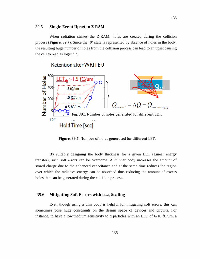
39.5 Single Event Upset in Z-RAM
When radiation strikes the Z-RAM, holes are created during the collision
process (Figure. 39.7). Since the ‘0’ state is represented by absence of holes in the body,
the resulting huge number of holes from the collision process can lead to an upset causing
the cell to read as logic ‘1’.
By suitably designing the body thickness for a given LET (Linear energy
transfer), such soft errors can be overcome. A thinner body increases the amount of
stored charge due to the enhanced capacitance and at the same time reduces the region
over which the radiative energy can be absorbed thus reducing the amount of excess
holes that can be generated during the collision process.
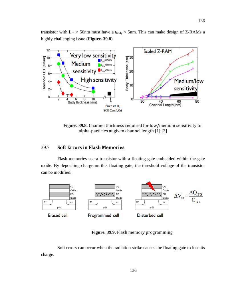
39.6 Mitigating Soft Errors with tbody Scaling
Even though using a thin body is helpful for mitigating soft errors, this can
sometimes pose huge constraints on the design space of devices and circuits. For
instance, to have a low/medium sensitivity to α particles with an LET of 6-10 fC/um, a
Figure. 39.7. Number of holes generated for different LET.
Fig. 39.1 Number of holes generated for different LET.
136
136
transistor with Lch > 50nm must have a tbody < 5nm. This can make design of Z-RAMs a
highly challenging issue (Figure. 39.8)
39.7 Soft Errors in Flash Memories
Flash memories use a transistor with a floating gate embedded within the gate
oxide. By depositing charge on this floating gate, the threshold voltage of the transistor
can be modified.
Soft errors can occur when the radiation strike causes the floating gate to lose its
charge.
Figure. 39.9. Flash memory programming.
Figure. 39.8. Channel thickness required for low/medium sensitivity to
alpha-particles at given channel length.[1],[2]

137
137
39.8 Charge loss and Single Event Upset in Flash Memories
Radiation strike generates electron-hole pairs as well as hot phonons due to
heating. The interaction between electron-hole pairs and the phonons leads to carrier
fluxes out of the floating gate (Figure. 39.10).
In older technologies with thick oxides, the carrier flux was due to charge
carriers hopping through localized states in the oxide. Some of the carriers would get
trapped in the oxide. In modern technologies with ultra-thin oxide, the transport is mostly
ballistic and can lead to TDDB (Figure. 39.11).
Figure. 39.10. Radiation induced carrier fluxes lead to charge losses in flash memories.

138
138
39.9 Transient Simulation Approach
The Geant4 high energy particle Physics toolkit can be used to simulate
ionization and relaxation within the oxide happening during a radiation strike. For
instance, the output of a simulation showing the ionization showers resulting from a high
energy chloride ion strike is shown in Figure. 39.12
Figure. 39.12 Chloride ion strike and ionization tracks resulting from Geant4 simulation.
Figure. 39.11. Older vs newer technologies.

139
139
The energy relaxation occurs chiefly due to phonon scattering and carrier
emission over oxide (Figure. 39.13).
39.10 Sensitivity of Floating Gate Cell Generations
As flash memory scales every generation, the amount of charge stored in the
floating gate is reducing. This is making them prone to upsets by radiation strikes since
the charge needed for upsetting the operation is now lower (Figure. 39.14). Thus the
sensitivity of flash memory technology to radiation effects is increasing. Error correction
may become necessary for such generations of flash technology.
Figure. 39.13 Energy relaxation in oxide after chloride ion strike.

140
140
39.11 Generation of Permanent Defects
The carrier outflow through the oxide can give rise to traps within the oxide
leading to a SILC like leakage. To estimate this, the Boltzmann equation is solved to get
the carrier distribution as a function of time. Phonon scattering, ionized impurity
scattering/impact ionization are treated using a full band ensemble Monte Carlo analysis.
Figure. 39.14 Sensitivity of flash to radiation effect is increasing with every
technology node.[3]

141
141
39.12 Conclusions
The footprint of memory is increasing rapidly with every technology generation.
It was seen that as memory scales, it becomes susceptible to radiation damage. ZRAM
due to its simple structure and high density is likely to replace the 1T-1C DRAM
memories. But soft errors in ZRAM remains an issue. Similarly in flash memories, soft
errors due to radiation strikes arise but this is owing to hot electron outflow from the
floating gate. Error correction is necessary for handling such errors. Finally it was seen
that hard errors can occur in flash due to oxide trap formation by hot electron outflow
leading to a SILC like leakage characteristics. This is a big reliability concern for flash
memories.
Figure. 39.15 Oxide trap generation and radiation induced leakage current.
142
142
39.13 References
1. “Scaling Limits of Double-Gate and Surround Gate Z-RAM Cells,” N. Butt and M.
A. Alam, , IEEE Transaction on Electron Devices, Special Issue on Modeling and Simulation, 54(9), pp. 2255-2262, 2007.
2. “Soft Error Trends and New Physical Model for Ionizing Dose Effects in Double Gate Z-RAM Cell,” N. Butt and M. A. Alam, IEEE Trans. on Nuclear Science, 54(6), pp. 2363-2370, 2007.
3. “Single Event Upsets in Floating Gate Memory Cells,” N. Z. Butt, and M. A. Alam, Proc. of International Reliability Physics Symposium, Apr 2008, pp. 547-555.
4. Soft Errors Induced by Natural Radiation by Ground Level in Floating Gate Memories, G. Just, et al. IRPS Proc. 2013.
5. “Soft Error Performance of Z-RAM Floating Body Memories”, D. Fisch, R. Beffa, C. Bassin, 2006 SOI Conference, p. 111.
6. “Alpha-particle induced upsets in advanced CMOS circuits and technology”, D. F. Heidel et al. IBM J. of Research and Dev 52(3), p. 225, May 2008.
7. “SEMM-2: A few generation of single-event-effect modeling tools”, H.H.K. Tang, IBM J. Res. And Dev. 52(3), p . 233.
8. “Circuit design and modeling for soft errors”, A. KleinOsowski, IBM J. of Research and Dev. 52(3), p. 255, May 2008.