3a dual channel synchronous step-down switcher with … · 2017-04-29 · 15 16 sgnd sgnd c11 vo1...
TRANSCRIPT
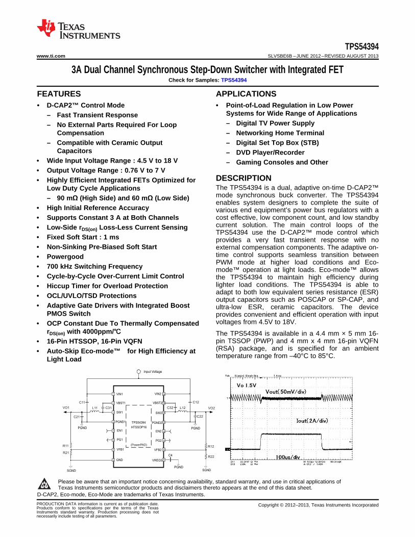
Input Voltage
PGND
PGND
C4
SW1
VIN1
VBST1
EN1
VFB2VFB1
GND VREG5
PGND1
6
VIN2
VBST2
EN2
SW2
PG1
5
1
3
PG2
9
10
11
PGND2
2
4
7
13
12
TPS54394
HTSSOP16
14
8
15
16
PGND
SGND SGND
C11
VO1
C21
R11
R21
L11 C31 C32 L12
C12
VO2
C22
R12
R22
(PowerPAD)
TPS54394www.ti.com SLVSBE6B –JUNE 2012–REVISED AUGUST 2013
3A Dual Channel Synchronous Step-Down Switcher with Integrated FETCheck for Samples: TPS54394
1FEATURES APPLICATIONS2• D-CAP2™ Control Mode • Point-of-Load Regulation in Low Power
Systems for Wide Range of Applications– Fast Transient Response– Digital TV Power Supply– No External Parts Required For Loop
Compensation – Networking Home Terminal– Compatible with Ceramic Output – Digital Set Top Box (STB)
Capacitors – DVD Player/Recorder• Wide Input Voltage Range : 4.5 V to 18 V – Gaming Consoles and Other• Output Voltage Range : 0.76 V to 7 V
DESCRIPTION• Highly Efficient Integrated FETs Optimized forThe TPS54394 is a dual, adaptive on-time D-CAP2™Low Duty Cycle Applicationsmode synchronous buck converter. The TPS54394– 90 mΩ (High Side) and 60 mΩ (Low Side) enables system designers to complete the suite of
• High Initial Reference Accuracy various end equipment’s power bus regulators with acost effective, low component count, and low standby• Supports Constant 3 A at Both Channelscurrent solution. The main control loops of the• Low-Side rDS(on) Loss-Less Current SensingTPS54394 use the D-CAP2™ mode control which
• Fixed Soft Start : 1 ms provides a very fast transient response with no• Non-Sinking Pre-Biased Soft Start external compensation components. The adaptive on-
time control supports seamless transition between• PowergoodPWM mode at higher load conditions and Eco-• 700 kHz Switching Frequency mode™ operation at light loads. Eco-mode™ allows
• Cycle-by-Cycle Over-Current Limit Control the TPS54394 to maintain high efficiency duringlighter load conditions. The TPS54394 is able to• Hiccup Timer for Overload Protectionadapt to both low equivalent series resistance (ESR)• OCL/UVLO/TSD Protections output capacitors such as POSCAP or SP-CAP, and
• Adaptive Gate Drivers with Integrated Boost ultra-low ESR, ceramic capacitors. The devicePMOS Switch provides convenient and efficient operation with input
voltages from 4.5V to 18V.• OCP Constant Due To Thermally CompensatedrDS(on) with 4000ppm/ The TPS54394 is available in a 4.4 mm × 5 mm 16-
pin TSSOP (PWP) and 4 mm x 4 mm 16-pin VQFN• 16-Pin HTSSOP, 16-Pin VQFN(RSA) package, and is specified for an ambient• Auto-Skip Eco-mode™ for High Efficiency attemperature range from –40°C to 85°C.Light Load
1
Please be aware that an important notice concerning availability, standard warranty, and use in critical applications ofTexas Instruments semiconductor products and disclaimers thereto appears at the end of this data sheet.
2D-CAP2, Eco-mode, Eco-Mode are trademarks of Texas Instruments.PRODUCTION DATA information is current as of publication date. Copyright © 2012–2013, Texas Instruments IncorporatedProducts conform to specifications per the terms of the TexasInstruments standard warranty. Production processing does notnecessarily include testing of all parameters.

TPS54394SLVSBE6B –JUNE 2012–REVISED AUGUST 2013 www.ti.com
These devices have limited built-in ESD protection. The leads should be shorted together or the device placed in conductive foamduring storage or handling to prevent electrostatic damage to the MOS gates.
ORDERING INFORMATION (1)
TA PACKAGE (2) (3) ORDERING PART NUMBER PINS OUTPUT SUPPLYTPS54394PWPR Tape-and-Reel
PWP 16TPS54394PWP Tube
–40 to 85TPS54394RSAR
RSA 16 Tape-and-ReelTPS54394RSAT
(1) For the most current package and ordering information, see the Package Option Addendum at the end of this document, or see the TIweb site at www.ti.com
(2) Package drawings, thermal data, and symbolization are available at www.ti.com/packaging.(3) All packaging options have Cu NIPDAU lead/ball finish.
ABSOLUTE MAXIMUM RATINGSover operating free-air temperature range (unless otherwise noted) (1) (2)
VALUE UNITMIN MAX
VIN1, VIN2, EN1, EN2 –0.3 20VBST1, VBST2 –0.3 26VBST1, VBST2 (10ns transient) –0.3 28
Input voltage range VBST1–SW1 , VBST2–SW2 –0.3 6.5 VVFB1, VFB2 –0.3 6.5SW1, SW2 –2 20SW1, SW2 (10ns transient) –4.5 22VREG5, PG1, PG2 –0.3 6.5
Output voltage range VPGND1, PGND2 –0.3 0.3Human Body Model (HBM) 2 kV
Electrostatic dischargeCharged Device Model (CDM) 500 V
TA Operating ambient temperature range –40 85 °CTSTG Storage temperature range –55 150 °CTJ Junction temperature range –40 150 °C
(1) Stresses beyond those listed under "absolute maximum ratings" may cause permanent damage to the device. These are stress ratingsonly and functional operation of the device at these or any other conditions beyond those indicated under "recommended operatingconditions" are not implied. Exposure to absolute-maximum-rated conditions for extended periods may affect device reliability.
(2) All voltages are with respect to IC GND terminal.
THERMAL INFORMATIONTPS54394
THERMAL METRIC (1) UNITSPWP (16) PINS RSA (16) PINS
θJA Junction-to-ambient thermal resistance 41.4 32.8θJCtop Junction-to-case (top) thermal resistance 27.1 35.4θJB Junction-to-board thermal resistance 20.8 9.9
°C/WψJT Junction-to-top characterization parameter 1.0 0.4ψJB Junction-to-board characterization parameter 20.6 10.0θJCbot Junction-to-case (bottom) thermal resistance 2.7 1.6
(1) For more information about traditional and new thermal metrics, see the IC Package Thermal Metrics application report, SPRA953.
2 Submit Documentation Feedback Copyright © 2012–2013, Texas Instruments Incorporated
Product Folder Links :TPS54394

TPS54394www.ti.com SLVSBE6B –JUNE 2012–REVISED AUGUST 2013
RECOMMENDED OPERATING CONDITIONSover operating free-air temperature range (unless otherwise noted)
VALUESUNIT
MIN MAXSupply input voltage range VIN1, VIN2 4.5 18 V
VBST1, VBST2 –0.1 24VBST1, VBST2 (10ns transient) –0.1 27VBST1–SW1, VBST2–SW2 –0.1 5.7
Input voltage range VFB1, VFB2 –0.1 5.7 VEN1, EN2 –0.1 18SW1, SW2 –1.0 18SW1, SW2 (10ns transient) –4.5 21VREG5, PG1 , PG2 –0.1 5.7
Output voltage range PGND1, PGND2 –0.1 0.1 VVO1, VO2 0.76 7.0
TA Operating free-air temperature –40 85 °CTJ Operating Junction Temperature –40 150 °C
ELECTRICAL CHARACTERISTICS (1)
over recommended free-air temperature range, VIN = 12 V (unless otherwise noted)PARAMETER CONDITIONS MIN TYP MAX UNIT
SUPPLY CURRENTTA = 25°C, EN1 = EN2 = 5 V,IIN VIN supply current 1200 2000 µAVFB1 = VFB2 = 0.8 V
IVINSDN VIN shutdown current TA = 25°C, EN1 = EN2 = 0 V, 15 20 µAFEEDBACK VOLTAGEVVFBTHLx VFBx threshold voltage TA = 25°C, CH1 = 3.3 V, CH2 = 1.5 V 758 765 773 mVTCVFBx Temperature coefficient On the basis of 25°C (2) –115 115 ppm/IVFBx VFB Input Current VFBx = 0.8 V, TA = 25°C –0.4 0.2 0.4 µAVREG5 OUTPUT
TA = 25°C, 6 V < VIN1 < 18 V,VVREG5 VREG5 output voltage 5.5 VIVREG = 5 mAVIN1 = 6 V, VREG5 = 4.0 V,IVREG5 Output current 75 mATA = 25°C (2)
MOSFETsrDS(on)H High side switch resistance TA = 25, VBSTx-SWx = 5.5 V (2) 90 mΩrDS(on)L Low side switch resistance TA = 25 (2) 60 mΩON-TIME TIMER CONTROLTON1 SW1 On Time SW1 = 12 V, VO1 = 1.2 V 165 nsTON2 SW2 On Time SW2 = 12 V, VO2 = 1.2 V 165 nsTOFF1 SW1 Min off time TA = 25, VFB1 = 0.7 V (2) 220 nsTOFF2 SW2 Min off time TA = 25, VFB2 = 0.7 V (2) 220 nsSOFT STARTTSS Soft-start time Internal soft-start time 1.0 ms
(1) x means either 1 or 2, that is, VFBx means VFB1 or VFB2.(2) Specified by design. Not production tested.
Copyright © 2012–2013, Texas Instruments Incorporated Submit Documentation Feedback 3
Product Folder Links :TPS54394

TPS54394SLVSBE6B –JUNE 2012–REVISED AUGUST 2013 www.ti.com
ELECTRICAL CHARACTERISTICS(1) (continued)over recommended free-air temperature range, VIN = 12 V (unless otherwise noted)
PARAMETER CONDITIONS MIN TYP MAX UNITPOWER GOOD
PG from lower VOx (going high) 84%VPGTH PGx threshold
PG from higher VOx (going low) 116%RPG PGx pull-down resistance VPGx = 0.5 V 50 75 110 Ω
Delay for PGx going high 1.5 msTPGDLY PGx delay time
Delay for PGx going low 2 µsTPGCOMPSS PGx comparator start-up delay PGx comparator wake-up delay 1.5 msUVLO
VREG5 rising 3.83VUVREG5 VREG5 UVLO threshold V
Hysteresis 0.6LOGIC THRESHOLDsVENH ENx H-level threshold voltage 2.0 VVENL ENx L-level threshold voltage 0.4 VRENx_IN ENx input resistance ENx = 12 V 225 450 900 kΩCURRENT LIMITsIOCL Current limit LOUT = 2.2 µH (3) 3.5 4.7 6.5 AOUTPUT UNDERVOLTAGE PROTECTION (UVP)VUVP Output UVP trip threshold measured on VFBx 63% 68% 73%TUVPDEL Output UVP delay time 1.5 msTUVPEN Output UVP enable delay 1.5 msTHERMAL SHUTDOWN
Shutdown temperature (3) 155TSD Thermal shutdown threshold °C
Hysteresis (3) 25
(3) Specified by design. Not production tested.
4 Submit Documentation Feedback Copyright © 2012–2013, Texas Instruments Incorporated
Product Folder Links :TPS54394

SW1
VIN1
VBST1
EN1
VFB2VFB1
GND VREG5
PGND1
6
VIN2
VBST2
EN2
SW2
PG1
5
1
3
PG2
9
10
11
PGND2
2
4
7
13
12
14
8
15
16
TPS54394
HTSSOP16
(PowerPAD)
PowerPAD
VFB1
VFB2
VIN1
SW
2
VBST2
VBST1
EN
1
14
75 6
2
3
4
1
PG
ND
2P
GN
D1
SW
1
VIN2
13
12
11
9
8
PG
1
10 GND
PG
2
EN
2
16 15
VREG5
TPS54394www.ti.com SLVSBE6B –JUNE 2012–REVISED AUGUST 2013
DEVICE INFORMATION
HTSSOP PACKAGERSA PACKAGE (TOP VIEW)(TOP VIEW)
PIN FUNCTIONS (1)
PINI/O DESCRIPTION
NAME PWP RSAVIN1 1 3 I Power inputs and connects to both high side NFET drains.
Supply Input for 5.5 V linear regulator.VIN2 16 2 IVBST1 2 4 I Supply input for high-side NFET gate drive circuit. Connect 0.1 µF ceramic capacitor
between VBSTx and SWx pins. An internal diode is connected between VREG5 andVBST2 15 1 I VBSTxSW1 3 5 I/O Switch node connections for both the high-side NFETs and low–side NFETs. Input of
current comparator.SW2 14 16 I/OPGND1 4 6 I/O
Ground returns for low-side MOSFETs. Input of current comparator.PGND2 13 15 I/OEN1 5 7 I
Enable. Pull High to enable according converter.EN2 12 14 IPG1 6 8 O Open drain power good output. Low means the output voltage of the corresponding
output is out of regulation.PG2 11 13 OVFB1 7 9 I
D-CAP2 feedback inputs. Connect to output voltage with resistor divider.VFB2 10 12 IGND 8 10 I/O Signal GND. Connect sensitive SSx and VFBx returns to GND at a single point.
Output of 5.5 V linear regulator. Bypass to GND with a high-quality ceramic capacitor ofVREG5 9 11 O at least 1 µF. VREG5 is active when ENx is high.Exposed Thermal Back Back Thermal pad of the package. Must be soldered to achieve appropriate dissipation. MustI/OPad side side be connected to GND.
(1) x means either 1 or 2, that is, VFBx means VFB1 or VFB2.
Copyright © 2012–2013, Texas Instruments Incorporated Submit Documentation Feedback 5
Product Folder Links :TPS54394

SW1
VBST1
EN1
VFB2
VFB1
GNDVREG5
PGND1
VO1
VBST2
EN2
SW2VO2
VIN1
VIN2
5VREG
ENLogic EN Logic
Ref1
Ref 2 SS2
SS1
UV2
UV1UV2 UVLO
UVLO
Fixed
SoftStart
REF
TSD
Ref1Ref2
-32
UV1-32
SS1
SS2
PGND1
PGND2
-16%
+16%PG1
-16%
+16%PG2
CH1 Min-off timer
CH2Min-off timer
VIN1
VIN1
VIN2
PGND2
PGND2
SW2
Ref_OCL
OCP2
ZC2SW2
PGND1
SW1
Ref_OCL
OCP1 ZC1SW1
Control logic
1.0 µF
Control logic
0.1 µF
PG
Comp
Err
Comp
ProtectionLogic
0.1 µF
Err
Comp
PG
Comp
TPS54394SLVSBE6B –JUNE 2012–REVISED AUGUST 2013 www.ti.com
FUNCTIONAL BLOCK DIAGRAM
6 Submit Documentation Feedback Copyright © 2012–2013, Texas Instruments Incorporated
Product Folder Links :TPS54394

( )INx Ox OxOx(LL)
SW INx
V V V1I =
2 L1x V
- ´´
´ ´ f
TPS54394www.ti.com SLVSBE6B –JUNE 2012–REVISED AUGUST 2013
OVERVIEWThe TPS54394 is a 3A/3A dual synchronous step-down (buck) converter with two integrated N-channelMOSFETs for each channel. It operates using D-CAP2™ control mode. The fast transient response of D-CAP2™control reduces the required output capacitance to meet a specific level of performance. Proprietary internalcircuitry allows the use of low ESR output capacitors including ceramic and special polymer types.
DETAILED DESCRIPTION
PWM OperationThe main control loop of the TPS54394 is an adaptive on-time pulse width modulation (PWM) controller thatsupports a proprietary D-CAP2™ control mode. D-CAP2™ control combines constant on-time control with aninternal compensation circuit for pseudo-fixed frequency and low external component count configuration withboth low ESR and ceramic output capacitors. It is stable even with virtually no ripple at the output.
At the beginning of each cycle, the high-side MOSFET is turned on. This MOSFET is turned off when the internaltimer expires. This timer is set by the converter’s input voltage, VINx, and the output voltage, VOx, to maintain apseudo-fixed frequency over the input voltage range hence it is called adaptive on-time control. The timer is resetand the high-side MOSFET is turned on again when the feedback voltage falls below the nominal output voltage.An internal ramp is added to the reference voltage to simulate output voltage ripple, eliminating the need for ESRinduced output ripple from D-CAP™ control.
PWM Frequency and Adaptive On-Time ControlTPS54394 uses an adaptive on-time control scheme and does not have a dedicated on board oscillator. TheTPS54394 runs with a pseudo-fixed frequency of 700 kHz by using the input voltage and output voltage to setthe on-time timer. The on-time is inversely proportional to the input voltage and proportional to the output voltage,therefore, when the duty ratio is VOx/VINx, the frequency is constant.
Auto-Skip Eco-Mode™ ControlThe TPS54394 is designed with Auto-Skip Eco-mode™ to increase light load efficiency. As the output currentdecreases from heavy load condition, the inductor current also reduces and eventually comes to the point whereits ripple valley touches the zero level, which is the boundary between continuous conduction and discontinuousconduction modes. The rectifying MOSFET is turned off when zero inductor current is detected. As the loadcurrent further decreases the converter runs into discontinuous conduction mode. The on-time is kept almost thesame as it was in the continuous conduction mode because it takes longer to discharge the output capacitor withsmaller load current to the nominal output voltage. The transition point to the light load operation IOx(LL) currentcan be estimated with Equation 1with 700-kHz used as fSW.
(1)
Soft Start and Pre-Biased Soft StartThe TPS54394 has an internal, 1.0ms, soft-start for each channel. When the ENx pin becomes high, an internalDAC begins ramping up the reference voltage to the PWM comparator. Smooth control of the output voltage ismaintained during start up.
The TPS54394 contains a unique circuit to prevent current from being pulled from the output during startup if theoutput is pre-biased. When the soft-start commands a voltage higher than the pre-bias level (internal soft startbecomes greater than internal feedback voltage, VFBx), the controller slowly activates synchronous rectificationby starting the first low side FET gate driver pulses with a narrow on-time. It then increments that on-time on acycle-by-cycle basis until it coincides with the time dictated by (1-D), where D is the duty cycle of the converter.This scheme prevents the initial sinking of the pre-biased output, and ensures that the output voltage (VOx)starts and ramps up smoothly into regulation from pre-biased startup to normal mode operation.
Copyright © 2012–2013, Texas Instruments Incorporated Submit Documentation Feedback 7
Product Folder Links :TPS54394
TPS54394SLVSBE6B –JUNE 2012–REVISED AUGUST 2013 www.ti.com
POWERGOODThe TPS54394 has power-good outputs that are measured on VFBx. The power-good function is activated afterthe soft-start has finished. If the output voltage is within 16% of the target voltage, the internal comparatordetects the power good state and the power good signal becomes high after 1.5ms delay. During start-up, thisinternal delay starts after 1.5ms of the UVP Enable delay time to avoid a glitch of the power-good signal. If thefeedback voltage goes outside of ±16% of the target value, the power-good signal becomes low after 2µs.
Current Sensing and Over-Current ProtectionThe output over-current protection (OCP) is implemented using a cycle-by-cycle valley detection control circuit.The switch current is monitored by measuring the low-side FET switch voltage between the SWx and PGNDxpins. This voltage is proportional to the switch current and the on-resistance of the FET. To improve themeasurement accuracy, the voltage sensing is temperature compensated.
During the on-time of the high-side FET switch, the switch current increases at a linear rate determined by VINx,VOx, the on-time and the output inductor value. During the on-time of the low-side FET switch, this currentdecreases linearly. The average value of the switch current is the load current IOUTx. If the sensed voltage on thelow-side FET is above the voltage proportional to the current limit, the converter keeps the low-side switch onuntil the measured voltage falls below the voltage corresponding to the current limit and a new switching cyclebegins. In subsequent switching cycles, the on-time is set to the value determined for CCM and the current ismonitored in the same manner.
Important considerations for this type of over-current protection: The load current is one half of the peak-to-peakinductor current higher than the over-current threshold. Also when the current is being limited, the output voltagetends to fall as the demanded load current may be higher than the current available from the converter. Whenthe over current condition is removed, the output voltage returns to the regulated value. This protection is non-latching.
Undervoltage Protection and Hiccup ModeHiccup mode of operation protects the power supply from being damaged during an over-current fault condition.If the OCL comparator circuit detects an over-current event the output voltage falls. When the feedback voltagefalls below 68% of the reference voltage, the UVP comparator output goes high and an internal UVP delaycounter begins counting. After counting UVP delay time, the TPS54394 shuts off the power supply for a giventime (7x UVP Enable Delay Time) and then tries to re-start the power supply. If the over-load condition has beenremoved, the power supply starts and operates normally; otherwise, the TPS54394 detects another over-currentevent and shuts off the power supply again, repeating the previous cycle. Excess heat due to overload lasts foronly a short duration in the hiccup cycle, therefore the junction temperature of the power device is much lower.
UVLO ProtectionUnder-voltage lock out protection (UVLO) monitors the voltage of the VREG5 pin. When the VREG5 voltage is lowerthan the UVLO threshold, the TPS54394 shuts down. As soon as the voltage increases above the UVLOthreshold, the converter starts again.
Thermal ShutdownTPS54394 monitors its temperature. If the temperature exceeds the threshold value (typically 155°C), the deviceshuts down. When the temperature falls below the threshold, the IC starts again.
When VIN1 starts up and VREG5 output voltage is below its nominal value, the thermal shutdown threshold islower than 155°C. As long as VIN1 rises, TJ must be kept below 110°C.
8 Submit Documentation Feedback Copyright © 2012–2013, Texas Instruments Incorporated
Product Folder Links :TPS54394
0 2 4 6 8 10 12 14 16 18 20
V - Input Voltage - VI
3.2
3.22
3.24
3.26
3.28
3.3
3.32
3.34
3.36
3.38
3.4
V-
Ou
tpu
t V
olt
ag
e -
VO
I = 10 mAO
I = 1 AO
V = 18 VIN
0 0.5 1 1.5 2 2.5 3
I - Output Current - AO
1.45
1.46
1.47
1.48
1.49
1.5
1.51
1.52
1.53
1.54
1.55
V-
Ou
tpu
t V
olt
ag
e -
VO
V = 12 VIN
V = 5 VIN
0 0.5 1 1.5 2 2.5 3
I - Output Current - AO
3.2
3.22
3.24
3.26
3.28
3.3
3.32
3.34
3.36
3.38
3.4
V-
Ou
tpu
t V
olt
ag
e -
VO
V = 6 VIN
V = 12 VIN
V = 18 VIN
0
10
20
30
40
50
60
EN
In
pu
t C
urr
en
t -
Am
0 5 10 15 20
EN Input Voltage - V
EN1
EN2
-50 0 50 100 150
T - Junction Temperature - °CJ
0
200
400
600
800
1000
1200
1400
1600
1800
2000
I-
Su
pp
ly C
urr
en
t -
AC
Cm
VIN1 = VIN2 = 12 V,
EN1 = EN2 = ON
IIN
-50 0 50 100 150
T - Junction Temperature - °CJ
0
2
4
6
8
10
12
14
16
18
20
Ivccsd
n -
Sh
utd
ow
n C
urr
en
t -
Am
IVINSDN
TPS54394www.ti.com SLVSBE6B –JUNE 2012–REVISED AUGUST 2013
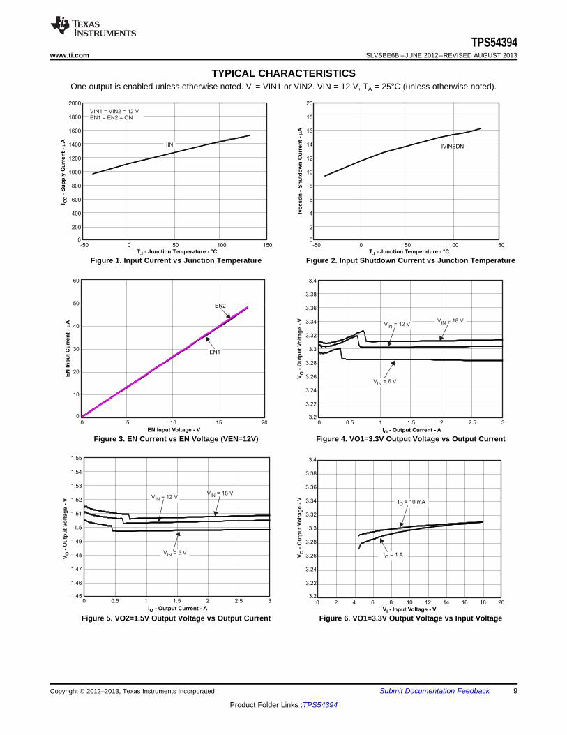
TYPICAL CHARACTERISTICSOne output is enabled unless otherwise noted. VI = VIN1 or VIN2. VIN = 12 V, TA = 25°C (unless otherwise noted).
Figure 1. Input Current vs Junction Temperature Figure 2. Input Shutdown Current vs Junction Temperature
Figure 3. EN Current vs EN Voltage (VEN=12V) Figure 4. VO1=3.3V Output Voltage vs Output Current
Figure 5. VO2=1.5V Output Voltage vs Output Current Figure 6. VO1=3.3V Output Voltage vs Input Voltage
Copyright © 2012–2013, Texas Instruments Incorporated Submit Documentation Feedback 9
Product Folder Links :TPS54394

40
50
60
70
80
90
100
Eff
icie
nc
y -
%
0 0.5 1 1.5 2 2.5 3
I - Output Current - AO
V = 6 VIN
V = 18 VIN
V = 12 VIN
Vout(50mV/div)
100 s/divm
Iout(2A/div)
1.45
1.46
1.47
1.48
1.49
1.5
1.51
1.52
1.53
1.54
1.55
V-
Ou
tpu
t V
olt
ag
e -
VO
0 2 4 6 8 10 12 14 16 18 20
V - Input Voltage - VI
I = 10 mAO
I = 1 AO
Iout(2A/div)
100 s/divm
Vout(50mV/div)
TPS54394SLVSBE6B –JUNE 2012–REVISED AUGUST 2013 www.ti.com
TYPICAL CHARACTERISTICS (continued)One output is enabled unless otherwise noted. VI = VIN1 or VIN2. VIN = 12 V, TA = 25°C (unless otherwise noted).
Figure 7. VO2=1.5V Output Voltage vs Input Voltage Figure 8. VO1=3.3V, 0A to 3A Load Transient Response
Figure 9. VO2=1.5V, 0A to 3A Load Transient Response Figure 10. VO1=3.3V, PG
Figure 11. VO2=1.5V, PG Figure 12. VO1=3.3V, Efficiency vs Output Current
10 Submit Documentation Feedback Copyright © 2012–2013, Texas Instruments Incorporated
Product Folder Links :TPS54394
I = 1 AO
0 2 4 6 8 10 12 14 16 18 20
V - Input Voltage - VI
400
450
500
550
600
650
700
750
800
fsw
- S
wit
ch
ing
Fre
qu
en
cy
- k
Hz
0.01 0.1 1 10
I - Output Current - AO
0
100
200
300
400
500
600
700
800
fsw
- S
wit
ch
ing
Fre
qu
en
cy
- k
Hz
V = 12 VIN
0 2 4 6 8 10 12 14 16 18 20
V - Input Voltage - VI
400
450
500
550
600
650
700
750
800
fsw
- S
wit
ch
ing
Fre
qu
en
cy -
kH
z
I = 1 AO
0
10
20
30
40
50
60
70
80
90
100
Eff
icie
nc
y -
%
0.001 0.1 10
I - Output Current - AO
0.01 1
V = 6 VIN
V = 12 VIN
V = 18 VIN
0
10
20
30
40
50
60
70
80
90
100
Eff
icie
ncy -
%
0.001 0.1 10
I - Output Current - AO
V = 6 VIN
V = 12 VIN
V = 18 VIN
0.01 1
40
50
60
70
80
90
100
Eff
icie
nc
y -
%
0 0.5 1 1.5 2 2.5 3
I - Output Current - AO
V = 5 VIN
V = 12 VIN
V = 18 VIN
TPS54394www.ti.com SLVSBE6B –JUNE 2012–REVISED AUGUST 2013
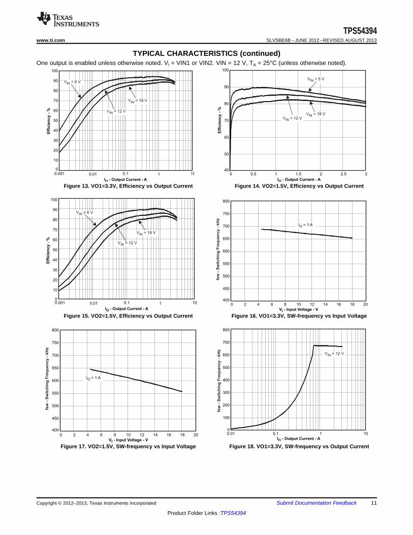
TYPICAL CHARACTERISTICS (continued)One output is enabled unless otherwise noted. VI = VIN1 or VIN2. VIN = 12 V, TA = 25°C (unless otherwise noted).
Figure 13. VO1=3.3V, Efficiency vs Output Current Figure 14. VO2=1.5V, Efficiency vs Output Current
Figure 15. VO2=1.5V, Efficiency vs Output Current Figure 16. VO1=3.3V, SW-frequency vs Input Voltage
Figure 17. VO2=1.5V, SW-frequency vs Input Voltage Figure 18. VO1=3.3V, SW-frequency vs Output Current
Copyright © 2012–2013, Texas Instruments Incorporated Submit Documentation Feedback 11
Product Folder Links :TPS54394

VIN2(50mV/div)
SW2(5V/div)
V = 1.5 VO
VIN1(50mV/div)
SW1(5V/div)
V = 3.3 VO
V 2(10mV/div)O
SW2(5V/div)
V = 1.5 VO
0
100
200
300
400
500
600
700
800
fsw
- S
wit
ch
ing
Fre
qu
en
cy -
kH
z
0.01 0.1 1 10
I - Output Current - AO
V = 12 VIN
V 1(10mV/div)O
SW1(5V/div)
V = 3.3 VO
TPS54394SLVSBE6B –JUNE 2012–REVISED AUGUST 2013 www.ti.com
TYPICAL CHARACTERISTICS (continued)One output is enabled unless otherwise noted. VI = VIN1 or VIN2. VIN = 12 V, TA = 25°C (unless otherwise noted).
Figure 19. VO2=1.5V, SW-frequency vs Output Current Figure 20. VO1=3.3V, VO1 Ripple Voltage (IO1= 3A)
Figure 21. VO2=1.5V, Ripple Voltage (IO2= 3A) Figure 22. VIN1 Input Voltage Ripple (IO1= 3A)
Figure 23. VIN2 Input Voltage Ripple (IO2= 3A)
12 Submit Documentation Feedback Copyright © 2012–2013, Texas Instruments Incorporated
Product Folder Links :TPS54394

P
OUT OUT
1F =
2 L C´p
Ox
R1xV = 0.765 V 1+
R2x
æ ö´ ç ÷
è ø
VINx
12V ± 10%
PGND
1uF
PGND
C4
SW1
VIN1
VBST1
EN1
VFB2VFB1
GND VREG5
PGND1
6
VIN2
VBST2
EN2
SW2
PG1
5
1
3
PG2
9
10
11
PGND2
2
4
7
13
12
TPS54394
HTSSOP16
14
8
15
16
PGND
SGND SGND
C11
10 FmVO1
3.3 V
C21
22 F
x2
m
R11
72.3 kW
R21
22.1 kW
L11
2.2 HmC31
0.1 Fm
C32
0.1 Fm
L12
1.5 Hm
C12
10 Fm VO2
1.5 V
C22
22 F
x2
m
R12
21.5 kW
R22
22.1 kW
TPS54394www.ti.com SLVSBE6B –JUNE 2012–REVISED AUGUST 2013
DESIGN GUIDE
Step By Step Design ProcedureTo begin the design process, you must know a few application parameters:• Input voltage range• Output voltage• Output current
In all formulas x is used to indicate that they are valid for both converters. For the calculations the estimatedswitching frequency of 700 kHz is used.
Figure 24. Schematic Diagram for the Design Example
Output Voltage Resistors SelectionThe output voltage is set with a resistor divider from the output node to the VFBx pin. It is recommended to use1% tolerance or better divider resistors. Start by using Equation 2 to calculate VOx.
To improve the efficiency at very light loads consider using larger value resistors, but too high resistance valueswill be more susceptible to noise and voltage errors due to the VFBx input current will be more noticeable.
(2)
Output Filter SelectionThe output filter used with the TPS54394 is an LC circuit. This LC filter has double pole at:
(3)
Copyright © 2012–2013, Texas Instruments Incorporated Submit Documentation Feedback 13
Product Folder Links :TPS54394

( )Ox INx OxCOx(RMS)
INx Ox SW
V V VI =
12 V L
´ -
´ ´ ´ f
2 2LOx(RMS) Ox L
1I = I + ΔI
12
LLpeakx Ox
ΔII = I +
2
INx(MAX) OxOxL1x
INx(MAX) SW
V VVΔI =
V L1x
-
´
´ f
TPS54394SLVSBE6B –JUNE 2012–REVISED AUGUST 2013 www.ti.com
At low frequencies, the overall loop gain is set by the output set-point resistor divider network and the internalgain of the TPS545394. The low frequency phase is 180 degrees. At the output filter pole frequency, the gainrolls off at a –40 dB per decade rate and the phase drops rapidly. D-CAP2™ introduces a high frequency zerothat reduces the gain roll off to –20 dB per decade and increases the phase to 90 degrees one decade above thezero frequency. The inductor and capacitor selected for the output filter must be selected so that the double poleof Equation 3 is located below the high frequency zero but close enough that the phase boost provided by thehigh frequency zero provides adequate phase margin for a stable circuit. To meet this requirement use thevalues recommended in Table 1.
Table 1. Recommended Component ValuesOUTPUT VOLTAGE (V) R1x (kΩ) R2x (kΩ) Cffx (pF) (1) L1x (µH) C2x (µF)
1 6.81 22.1 1.5 - 2.2 20 - 681.05 8.25 22.1 1.5 - 2.2 20 - 681.2 12.7 22.1 1.5 - 2.2 20 - 681.5 21.5 22.1 1.5 - 2.2 20 - 681.8 30.1 22.1 5 - 22 2.2 - 3.3 20 - 682.5 49.9 22.1 5 - 22 2.2 - 3.3 20 - 683.3 73.2 22.1 5 - 22 2.2 - 3.3 20 - 685 124 22.1 5 - 22 4.7 20 - 68
6.5 165 22.1 5 - 22 4.7 20 - 68
(1) Optional
For higher output voltages at or above 1.8 V, additional phase boost can be achieved by adding a feed forwardcapacitor (Cff) in parallel with R1.
The inductor peak-to-peak ripple current, peak current and RMS current are calculated using Equation 4,Equation 5 and Equation 6. The inductor saturation current rating must be greater than the calculated peakcurrent and the RMS or heating current rating must be greater than the calculated RMS current.
For the calculations, use 700 kHz as the switching frequency, fSW. Make sure the chosen inductor is rated for thepeak current of Equation 5 and the RMS current of Equation 6.
(4)
(5)
(6)
For the above design example, the calculated peak current is 3.46 A and the calculated RMS current is 3.01 Afor VO1. The inductor used is a TDK CLF7045-2R2N with a rated current of 5.5A based on the inductancechange and of 4.3A based on the temperature rise.
The capacitor value and ESR determines the amount of output voltage ripple. The TPS54394 is intended for usewith ceramic or other low ESR capacitors. The recommended value range is from 20µF to 68µF. Use Equation 7to determine the required RMS current rating for the output capacitor(s).
(7)
For this design two TDK C3216X5R0J226M 22µF output capacitors are used. The typical ESR is 2 mΩ each.The calculated RMS current is 0.19A and each output capacitor is rated for 4A.
14 Submit Documentation Feedback Copyright © 2012–2013, Texas Instruments Incorporated
Product Folder Links :TPS54394

TPS54394www.ti.com SLVSBE6B –JUNE 2012–REVISED AUGUST 2013
Input Capacitor SelectionThe TPS54394 requires an input decoupling capacitor and a bulk capacitor is needed depending on theapplication. A ceramic capacitor of or above 10µF is recommended for the decoupling capacitor. Additionally, 0.1µF ceramic capacitors from pin 1 and Pin 16 to ground are recommended to improve the stability and reduce theSWx node overshoots. The capacitors voltage rating needs to be greater than the maximum input voltage.
Bootstrap Capacitor SelectionA 0.1 µF ceramic capacitors must be connected between the VBSTx and SWx pins for proper operation. It isrecommended to use ceramic capacitors with a dielectric of X5R or better.
VREG5 Capacitor SelectionA 1 µF ceramic capacitor must be connected between the VREG5 and GND pins for proper operation. It isrecommended to use a ceramic capacitor with a dielectric of X5R or better.
Thermal InformationThis 16-pin PWP package incorporates an exposed thermal pad. The thermal pad must be soldered directly tothe printed circuit board (PCB). After soldering, the PCB is used as a heatsink. In addition, through the use ofthermal vias, the thermal pad can be attached directly to the appropriate copper plane shown in the electricalschematic for the device, or alternatively, can be attached to a special heatsink structure designed into the PCB.This design optimizes the heat transfer from the integrated circuit (IC).
For additional information on the exposed thermal pad and how to use the advantage of its heat dissipatingabilities, refer to the Technical Brief, PowerPAD™ Thermally Enhanced Package, Texas Instruments LiteratureNo. SLMA002 and Application Brief, PowerPAD™ Made Easy, Texas Instruments Literature No. SLMA004.
The exposed thermal pad dimensions for this package are shown in the following illustration.
Figure 25. Thermal Pad Dimensions
Layout Considerations1. Keep the input current loop as small as possible. And avoid the input switching current through the thermal
pad.2. Keep the SW node as physically small and short as possible to minimize parasitic capacitance and
inductance and to minimize radiated emissions.3. Keep analog and non-switching components away from switching components.4. Make a single point connection from the signal ground to power ground.5. Do not allow switching currents to flow under the device.6. Keep the pattern lines for VINx and PGNDx broad.
Copyright © 2012–2013, Texas Instruments Incorporated Submit Documentation Feedback 15
Product Folder Links :TPS54394

SW1
VIN1
VBST1
EN1
VFB1
GND VREG 5
PGND1
6
VIN2
VBST2
EN2
SW2
PG1
5
1
3
PG2
9
10
11
PGND2
2
4
7
13
12
14
8
15
16
VFB2
VIN2
BIASCAP
VIN HIGH
FREQUENCYBYPASS
CAPACITOR
~0.1µF
VIN INPUTBYPASS
CAPACITOR
10µF x2
OUTPUT
INDUCTOR
OUTPUTFILTER
CAPACITOR
POWER GND
TO ENABLECONTROL
Keepdistance more
than 1 inch
Recommend to keepdistance more than 3-4mm.
(to avoid noise scattering,especially GND plane.)
To feedback
resisters
VO2
Feedback
resisters
GND
PLANE2,3 or bottom
layer
Symmetrical Layoutfor CH1 and CH2
Switching noiseflows through IC
and CIN. It avoidsthe thermal Pad.
Via to GND Plane
- Blue parts can be placed on the bottom side- Connect the SWx pins through another layer with the inductor(yellow line)
TPS54394SLVSBE6B –JUNE 2012–REVISED AUGUST 2013 www.ti.com
7. Exposed pad of device must be soldered to PGND.8. VREG5 capacitor should be placed near the device, and connected to GND.9. Output capacitors should be connected with a broad pattern to the PGND.10. Voltage feedback loops should be as short as possible, and preferably with ground shields.11. Kelvin connections should be brought from the output to the feedback pin of the device.12. Providing sufficient vias is preferable for VIN, SW and PGND connections.13. PCB pattern for VIN, SW, and PGND should be as broad as possible.14. VIN Capacitor should be placed as near as possible to the device.
Figure 26. TPS54394 Layout
16 Submit Documentation Feedback Copyright © 2012–2013, Texas Instruments Incorporated
Product Folder Links :TPS54394

EXPOSED THERMALPAD AREA
BOOSTCAPACITOR
VOUT2
VIA to Internal orBottom Layer Ground Plane
OUTPUT2INDUCTOR
OUTPUT2FILTERCAPACITORS
TO POWERGOOD PULLUP 2
ANALOGGROUNDTRACE
VIN INPUTBYPASSCAPACITORS
VIN
FEEDBACKRESISTORS
Etch on Bottom Layer,Internal Layer orUnder Component
BIASCAP
VIN HIGHFREQUENCYBYPASSCAPACITOR
VBST1
SW
1S
W2
VIN1
VIN2
VFB1
VREG5
GND
PG
2
EN
2
PG
ND
2P
GN
D1
16
75 6
2
3
4
1
15
12
11
9
8
10
14 13
VFB2VBST2E
1N
PG
1
TO ENABLECONTROL
BOOSTCAPACITOR
OUTPUT1INDUCTOR
OUTPUT1FILTERCAPACITORS
VIN INPUTBYPASSCAPACITORS
FEEDBACKRESISTORS
POWERGROUND
VIN HIGHFREQUENCYBYPASSCAPACITOR
KEEPVIAS > 3-4 mmFROM OUTPUTCAPACITORS
KEEP OUTPUTVIAS > 25 mmFROM INPUT VIAS
KEEPVIAS > 3-4 mmFROM INPUTCAPACITORS
NOTE: IT IS POSSIBLE TO PLACESOME COMPONENTS SUCH ASBOOST CAPACITOR AND FEEDBACKRESISTORS ON BOTTOM LAYER
VOUT1
TO ENABLECONTROL
POWERGROUND
KEEPVIAS > 3-4 mmFROM OUTPUTCAPACITORS
KEEP OUTPUTVIAS > 25 mmFROM INPUT VIAS
KEEPVIAS > 3-4 mmFROM INPUTCAPACITORS
Internal or BottomLayer Ground Plane
VIA to internal orBottom Layer Etch
Etch or Copper Fillon Top Layer
INTERNAL ORBOTTOM LAYERGROUND PLANE
TO POWERGOOD PULLUP 1
TPS54394www.ti.com SLVSBE6B –JUNE 2012–REVISED AUGUST 2013
Figure 27. RSA Package Layout
Copyright © 2012–2013, Texas Instruments Incorporated Submit Documentation Feedback 17
Product Folder Links :TPS54394

TPS54394SLVSBE6B –JUNE 2012–REVISED AUGUST 2013 www.ti.com
REVISION HISTORY
Changes from Original (June 2012) to Revision A Page
• Added 16-pin VQFN to the Features and Description .......................................................................................................... 1• Added the RSA 16 pin package to the Ordering Information table ...................................................................................... 2• Added the RSA package to the Thermal Information table .................................................................................................. 2• Added the RSA 16 pin package pinout image, pin names and functions to the DEVICE INFORMATION section ............. 5• Added Figure 27 ................................................................................................................................................................. 17
Changes from Revision A (May 2013) to Revision B Page
• Changed the Abs Max Ratings table Input Voltage for SW1, SW2 (10ns transient) From: MIN = –0.3 V To: –4.5 V ......... 2• Changed θJA on the PWP (16) PINS package From: 47.5 To: 41.4 °C/W ........................................................................... 2• Changed the ROC table, Input Voltage for SW1, SW2 (10ns transient) From: MIN = –0.3 V To: –4.5 V ........................... 3• Change text in the Auto-Skip Eco-Mode™ Control section From: "The on-time is kept almost half as it was in the
continuous..." To: "The on-time is kept almost the same as it was in the continuous..." ..................................................... 7
18 Submit Documentation Feedback Copyright © 2012–2013, Texas Instruments Incorporated
Product Folder Links :TPS54394

PACKAGE OPTION ADDENDUM
www.ti.com 25-Jul-2013
Addendum-Page 1
PACKAGING INFORMATION
Orderable Device Status(1)
Package Type PackageDrawing
Pins PackageQty
Eco Plan(2)
Lead/Ball Finish MSL Peak Temp(3)
Op Temp (°C) Device Marking(4/5)
Samples
TPS54394PWP ACTIVE HTSSOP PWP 16 90 Green (RoHS& no Sb/Br)
CU NIPDAU Level-2-260C-1 YEAR -40 to 85 PS54394
TPS54394PWPR ACTIVE HTSSOP PWP 16 2000 Green (RoHS& no Sb/Br)
CU NIPDAU Level-2-260C-1 YEAR -40 to 85 PS54394
TPS54394RSAR ACTIVE QFN RSA 16 3000 Green (RoHS& no Sb/Br)
CU NIPDAU Level-2-260C-1 YEAR -40 to 85 TPS54394
TPS54394RSAT ACTIVE QFN RSA 16 250 Green (RoHS& no Sb/Br)
CU NIPDAU Level-2-260C-1 YEAR -40 to 85 TPS54394
(1) The marketing status values are defined as follows:ACTIVE: Product device recommended for new designs.LIFEBUY: TI has announced that the device will be discontinued, and a lifetime-buy period is in effect.NRND: Not recommended for new designs. Device is in production to support existing customers, but TI does not recommend using this part in a new design.PREVIEW: Device has been announced but is not in production. Samples may or may not be available.OBSOLETE: TI has discontinued the production of the device.
(2) Eco Plan - The planned eco-friendly classification: Pb-Free (RoHS), Pb-Free (RoHS Exempt), or Green (RoHS & no Sb/Br) - please check http://www.ti.com/productcontent for the latest availabilityinformation and additional product content details.TBD: The Pb-Free/Green conversion plan has not been defined.Pb-Free (RoHS): TI's terms "Lead-Free" or "Pb-Free" mean semiconductor products that are compatible with the current RoHS requirements for all 6 substances, including the requirement thatlead not exceed 0.1% by weight in homogeneous materials. Where designed to be soldered at high temperatures, TI Pb-Free products are suitable for use in specified lead-free processes.Pb-Free (RoHS Exempt): This component has a RoHS exemption for either 1) lead-based flip-chip solder bumps used between the die and package, or 2) lead-based die adhesive used betweenthe die and leadframe. The component is otherwise considered Pb-Free (RoHS compatible) as defined above.Green (RoHS & no Sb/Br): TI defines "Green" to mean Pb-Free (RoHS compatible), and free of Bromine (Br) and Antimony (Sb) based flame retardants (Br or Sb do not exceed 0.1% by weightin homogeneous material)
(3) MSL, Peak Temp. -- The Moisture Sensitivity Level rating according to the JEDEC industry standard classifications, and peak solder temperature.
(4) There may be additional marking, which relates to the logo, the lot trace code information, or the environmental category on the device.
(5) Multiple Device Markings will be inside parentheses. Only one Device Marking contained in parentheses and separated by a "~" will appear on a device. If a line is indented then it is a continuationof the previous line and the two combined represent the entire Device Marking for that device.
Important Information and Disclaimer:The information provided on this page represents TI's knowledge and belief as of the date that it is provided. TI bases its knowledge and belief on informationprovided by third parties, and makes no representation or warranty as to the accuracy of such information. Efforts are underway to better integrate information from third parties. TI has taken and

PACKAGE OPTION ADDENDUM
www.ti.com 25-Jul-2013
Addendum-Page 2
continues to take reasonable steps to provide representative and accurate information but may not have conducted destructive testing or chemical analysis on incoming materials and chemicals.TI and TI suppliers consider certain information to be proprietary, and thus CAS numbers and other limited information may not be available for release.
In no event shall TI's liability arising out of such information exceed the total purchase price of the TI part(s) at issue in this document sold by TI to Customer on an annual basis.
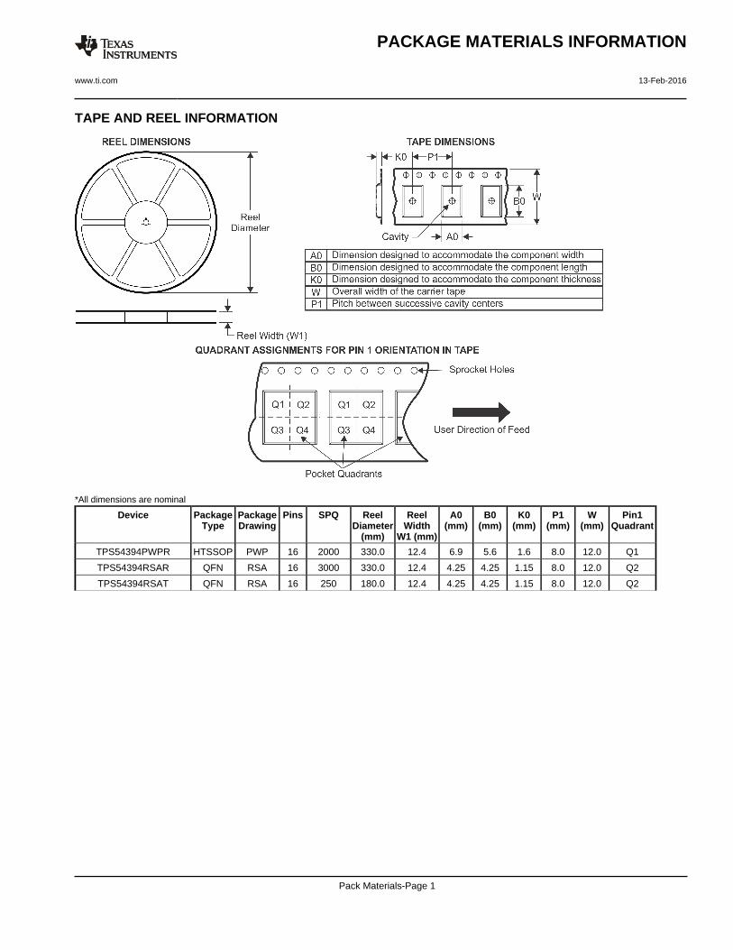
TAPE AND REEL INFORMATION
*All dimensions are nominal
Device PackageType
PackageDrawing
Pins SPQ ReelDiameter
(mm)
ReelWidth
W1 (mm)
A0(mm)
B0(mm)
K0(mm)
P1(mm)
W(mm)
Pin1Quadrant
TPS54394PWPR HTSSOP PWP 16 2000 330.0 12.4 6.9 5.6 1.6 8.0 12.0 Q1
TPS54394RSAR QFN RSA 16 3000 330.0 12.4 4.25 4.25 1.15 8.0 12.0 Q2
TPS54394RSAT QFN RSA 16 250 180.0 12.4 4.25 4.25 1.15 8.0 12.0 Q2
PACKAGE MATERIALS INFORMATION
www.ti.com 13-Feb-2016
Pack Materials-Page 1

*All dimensions are nominal
Device Package Type Package Drawing Pins SPQ Length (mm) Width (mm) Height (mm)
TPS54394PWPR HTSSOP PWP 16 2000 367.0 367.0 38.0
TPS54394RSAR QFN RSA 16 3000 367.0 367.0 35.0
TPS54394RSAT QFN RSA 16 250 210.0 185.0 35.0
PACKAGE MATERIALS INFORMATION
www.ti.com 13-Feb-2016
Pack Materials-Page 2


www.ti.com
PACKAGE OUTLINE
C
14X 0.65
2X4.55
16X 0.300.19
TYP6.66.2
0.150.05
0.25GAGE PLANE
-80
1.2 MAX3.552.68
2.461.75
B 4.54.3
A
NOTE 3
5.14.9
0.750.50
(0.15) TYP
PowerPAD TSSOP - 1.2 mm max heightPWP0016JSMALL OUTLINE PACKAGE
4223595/A 03/2017
1
89
16
0.1 C A B
PIN 1 INDEXAREA
SEE DETAIL A
0.1 C
NOTES: 1. All linear dimensions are in millimeters. Any dimensions in parenthesis are for reference only. Dimensioning and tolerancing per ASME Y14.5M. 2. This drawing is subject to change without notice. 3. This dimension does not include mold flash, protrusions, or gate burrs. Mold flash, protrusions, or gate burrs shall not exceed 0.15 mm per side. 4. Reference JEDEC registration MO-153.
SEATINGPLANE
TM
PowerPAD is a trademark of Texas Instruments.
A 20DETAIL ATYPICAL
SCALE 2.500
THERMALPAD
1
8 9
16

www.ti.com
EXAMPLE BOARD LAYOUT
0.05 MAXALL AROUND
0.05 MINALL AROUND
16X (1.5)
16X (0.45)
14X (0.65)
(5.8)
(R0.05) TYP
(3.4)NOTE 8
(5)NOTE 8
(1.35) TYP
(0.65)
(1.3) TYP
( 0.2) TYPVIA
(2.46)
(3.55)
PowerPAD TSSOP - 1.2 mm max heightPWP0016JSMALL OUTLINE PACKAGE
4223595/A 03/2017
NOTES: (continued) 5. Publication IPC-7351 may have alternate designs. 6. Solder mask tolerances between and around signal pads can vary based on board fabrication site. 7. This package is designed to be soldered to a thermal pad on the board. For more information, see Texas Instruments literature numbers SLMA002 (www.ti.com/lit/slma002) and SLMA004 (www.ti.com/lit/slma004). 8. Size of metal pad may vary due to creepage requirement. 9. Vias are optional depending on application, refer to device data sheet. It is recommended that vias under paste be filled, plugged or tented.
TM
SEE DETAILS
LAND PATTERN EXAMPLEEXPOSED METAL SHOWN
SCALE: 10X
SYMM
SYMM
1
8 9
16
METAL COVEREDBY SOLDER MASK
SOLDER MASKDEFINED PAD
15.000
METALSOLDER MASKOPENING
METAL UNDERSOLDER MASK
SOLDER MASKOPENING
EXPOSED METALEXPOSED METAL
SOLDER MASK DETAILS
NON-SOLDER MASKDEFINED
SOLDER MASKDEFINED
www.ti.com
EXAMPLE STENCIL DESIGN
16X (1.5)
16X (0.45)
14X (0.65)
(5.8)
(R0.05) TYP
(3.55)BASED ON
0.125 THICKSTENCIL
(2.46)BASED ON
0.125 THICKSTENCIL
PowerPAD TSSOP - 1.2 mm max heightPWP0016JSMALL OUTLINE PACKAGE
4223595/A 03/2017
2.08 X 3.000.1752.25 X 3.240.15
2.46 X 3.55 (SHOWN)0.1252.75 X 3.970.1
SOLDER STENCILOPENING
STENCILTHICKNESS
NOTES: (continued) 10. Laser cutting apertures with trapezoidal walls and rounded corners may offer better paste release. IPC-7525 may have alternate design recommendations. 11. Board assembly site may have different recommendations for stencil design.
TM
SOLDER PASTE EXAMPLEBASED ON 0.125 mm THICK STENCIL
SCALE: 10X
SYMM
SYMM
1
8 9
16
METAL COVEREDBY SOLDER MASK
SEE TABLE FORDIFFERENT OPENINGSFOR OTHER STENCILTHICKNESSES

IMPORTANT NOTICE
Texas Instruments Incorporated (TI) reserves the right to make corrections, enhancements, improvements and other changes to itssemiconductor products and services per JESD46, latest issue, and to discontinue any product or service per JESD48, latest issue. Buyersshould obtain the latest relevant information before placing orders and should verify that such information is current and complete.TI’s published terms of sale for semiconductor products (http://www.ti.com/sc/docs/stdterms.htm) apply to the sale of packaged integratedcircuit products that TI has qualified and released to market. Additional terms may apply to the use or sale of other types of TI products andservices.Reproduction of significant portions of TI information in TI data sheets is permissible only if reproduction is without alteration and isaccompanied by all associated warranties, conditions, limitations, and notices. TI is not responsible or liable for such reproduceddocumentation. Information of third parties may be subject to additional restrictions. Resale of TI products or services with statementsdifferent from or beyond the parameters stated by TI for that product or service voids all express and any implied warranties for theassociated TI product or service and is an unfair and deceptive business practice. TI is not responsible or liable for any such statements.Buyers and others who are developing systems that incorporate TI products (collectively, “Designers”) understand and agree that Designersremain responsible for using their independent analysis, evaluation and judgment in designing their applications and that Designers havefull and exclusive responsibility to assure the safety of Designers' applications and compliance of their applications (and of all TI productsused in or for Designers’ applications) with all applicable regulations, laws and other applicable requirements. Designer represents that, withrespect to their applications, Designer has all the necessary expertise to create and implement safeguards that (1) anticipate dangerousconsequences of failures, (2) monitor failures and their consequences, and (3) lessen the likelihood of failures that might cause harm andtake appropriate actions. Designer agrees that prior to using or distributing any applications that include TI products, Designer willthoroughly test such applications and the functionality of such TI products as used in such applications.TI’s provision of technical, application or other design advice, quality characterization, reliability data or other services or information,including, but not limited to, reference designs and materials relating to evaluation modules, (collectively, “TI Resources”) are intended toassist designers who are developing applications that incorporate TI products; by downloading, accessing or using TI Resources in anyway, Designer (individually or, if Designer is acting on behalf of a company, Designer’s company) agrees to use any particular TI Resourcesolely for this purpose and subject to the terms of this Notice.TI’s provision of TI Resources does not expand or otherwise alter TI’s applicable published warranties or warranty disclaimers for TIproducts, and no additional obligations or liabilities arise from TI providing such TI Resources. TI reserves the right to make corrections,enhancements, improvements and other changes to its TI Resources. TI has not conducted any testing other than that specificallydescribed in the published documentation for a particular TI Resource.Designer is authorized to use, copy and modify any individual TI Resource only in connection with the development of applications thatinclude the TI product(s) identified in such TI Resource. NO OTHER LICENSE, EXPRESS OR IMPLIED, BY ESTOPPEL OR OTHERWISETO ANY OTHER TI INTELLECTUAL PROPERTY RIGHT, AND NO LICENSE TO ANY TECHNOLOGY OR INTELLECTUAL PROPERTYRIGHT OF TI OR ANY THIRD PARTY IS GRANTED HEREIN, including but not limited to any patent right, copyright, mask work right, orother intellectual property right relating to any combination, machine, or process in which TI products or services are used. Informationregarding or referencing third-party products or services does not constitute a license to use such products or services, or a warranty orendorsement thereof. Use of TI Resources may require a license from a third party under the patents or other intellectual property of thethird party, or a license from TI under the patents or other intellectual property of TI.TI RESOURCES ARE PROVIDED “AS IS” AND WITH ALL FAULTS. TI DISCLAIMS ALL OTHER WARRANTIES ORREPRESENTATIONS, EXPRESS OR IMPLIED, REGARDING RESOURCES OR USE THEREOF, INCLUDING BUT NOT LIMITED TOACCURACY OR COMPLETENESS, TITLE, ANY EPIDEMIC FAILURE WARRANTY AND ANY IMPLIED WARRANTIES OFMERCHANTABILITY, FITNESS FOR A PARTICULAR PURPOSE, AND NON-INFRINGEMENT OF ANY THIRD PARTY INTELLECTUALPROPERTY RIGHTS. TI SHALL NOT BE LIABLE FOR AND SHALL NOT DEFEND OR INDEMNIFY DESIGNER AGAINST ANY CLAIM,INCLUDING BUT NOT LIMITED TO ANY INFRINGEMENT CLAIM THAT RELATES TO OR IS BASED ON ANY COMBINATION OFPRODUCTS EVEN IF DESCRIBED IN TI RESOURCES OR OTHERWISE. IN NO EVENT SHALL TI BE LIABLE FOR ANY ACTUAL,DIRECT, SPECIAL, COLLATERAL, INDIRECT, PUNITIVE, INCIDENTAL, CONSEQUENTIAL OR EXEMPLARY DAMAGES INCONNECTION WITH OR ARISING OUT OF TI RESOURCES OR USE THEREOF, AND REGARDLESS OF WHETHER TI HAS BEENADVISED OF THE POSSIBILITY OF SUCH DAMAGES.Unless TI has explicitly designated an individual product as meeting the requirements of a particular industry standard (e.g., ISO/TS 16949and ISO 26262), TI is not responsible for any failure to meet such industry standard requirements.Where TI specifically promotes products as facilitating functional safety or as compliant with industry functional safety standards, suchproducts are intended to help enable customers to design and create their own applications that meet applicable functional safety standardsand requirements. Using products in an application does not by itself establish any safety features in the application. Designers mustensure compliance with safety-related requirements and standards applicable to their applications. Designer may not use any TI products inlife-critical medical equipment unless authorized officers of the parties have executed a special contract specifically governing such use.Life-critical medical equipment is medical equipment where failure of such equipment would cause serious bodily injury or death (e.g., lifesupport, pacemakers, defibrillators, heart pumps, neurostimulators, and implantables). Such equipment includes, without limitation, allmedical devices identified by the U.S. Food and Drug Administration as Class III devices and equivalent classifications outside the U.S.TI may expressly designate certain products as completing a particular qualification (e.g., Q100, Military Grade, or Enhanced Product).Designers agree that it has the necessary expertise to select the product with the appropriate qualification designation for their applicationsand that proper product selection is at Designers’ own risk. Designers are solely responsible for compliance with all legal and regulatoryrequirements in connection with such selection.Designer will fully indemnify TI and its representatives against any damages, costs, losses, and/or liabilities arising out of Designer’s non-compliance with the terms and provisions of this Notice.
Mailing Address: Texas Instruments, Post Office Box 655303, Dallas, Texas 75265Copyright © 2017, Texas Instruments Incorporated