3d board level x-ray inspection via limited angle …
TRANSCRIPT

3D BOARD LEVEL X-RAY INSPECTION VIA LIMITED ANGLE COMPUTER
TOMOGRAPHY
David Bernard Ph.D. & Dragos Golubovic Ph.D.
Nordson DAGE
Aylesbury, Buckinghamshire, U.K.
Evstatin Krastev Ph.D.
Nordson DAGE Fremont, CA, USA
ABSTRACT
Computer Tomography (CT) is a powerful inspection
technique used widely in the electronics industry, especially
for the analysis of multi-layered devices and joint
interconnections. As the resolution required to be able to
inspect today’s devices is in the micron range, this aspect of
CT is often referred to as µCT so as to differentiate it from
medical and industrial CT applications where the same level
of resolution is not possible or required. The µCT technique
permits different layers / slices of the device to be isolated
and examined individually, so practically providing an
electronic, or virtual, cross-sectioning within the sample.
The benefits of an ‘electronic cross-section’ compared to
traditional mechanical cross-sectioning are many. These
include that the electronic cross-sectioning is reversible –
you cannot over polish and go too far into the sample - the
cutting plane can be positioned in any orientation within the
3D space of the CT model and no additional defects are
introduced or existing defects concealed compared with the
process of mechanically cutting, polishing and preparing the
sample for a cross-section. One of the limitations of
traditional µCT is that there is a restriction to the maximum
sample size that can be used to produce a µCT model with
reasonable speed, quality and analytical value. Usually, the
maximum practical size for a regular µCT is ~ 2” x 2” (50 x
50 mm). Thus, it is not possible to use the µCT technique
on a large PCB unless you are willing to cut around the
device / region of interest to be examined to make it small
enough for analysis, but in so doing destroying the board. In
order to overcome the sample size limitation of ‘full µCT’, a
‘limited angle’ or ‘partial’ µCT technique has been
developed and used in some X-Ray systems. This permits a
3D model to be created from devices / regions of interest
anywhere within a board without the need to destroy it. This
paper will explain the mechanism and differences between
full µCT and the various types of limited angle µCT and
compare different applications where one or the other
technique is applicable, backed by real life cases and
examples.
Key words: X-ray inspection, X-ray technology, Computer
Tomography, CT, Inclined CT, Partial CT, CT without
cutting.
INTRODUCTION
Many talented scientists have contributed to the instigation
and development of the computerized tomography
technique the way we know it now. In 1937, a Polish
mathematician, named Stefan Kaczmarz, developed a
method to find an approximate solution to a large system of
linear algebraic equations, which further developed into his
powerful reconstruction method the "Algebraic
Reconstruction Technique (ART)". This technique was later
adapted by Sir Godfrey Hounsfield as the image
reconstruction mechanism for his famous invention, the first
commercial CT scanner. William Oldendorf, a UCLA
neurologist and senior medical investigator at the West Los
Angeles Veterans Administration hospital, published a
landmark paper in 1961, where he described the basic
concept later used by Allan McLeod Cormack to develop
the mathematics behind computerized tomography (from
Wikipedia). These are some of the pioneering scientific
endeavors that paved the way to the remarkable
developments in the capabilities of medical diagnostic
radiology in the latter half of the 20th century. Initially, this
was through Computer (Aided) Tomography, which we
have come to know as CAT or CT scanning, and this was
subsequently followed by the other imaging techniques we
also now take for granted, such as MRI and PET scanning.
The needs of being able to look inside an object, without
opening it up, or destroying it, and separating the different
features that would otherwise overlap each other when seen
in a standard 2D x-ray image, are the same for electronics
inspection as they are in the medical sphere. If there is a
problem with a board (or a person!) ideally we want to
analyse the situation as much as possible with everything in
its natural, and untouched, state before we opt, if necessary,
to take more radical action to probe the fault location with
more invasive techniques and, possibly, a ‘surgical’, or
destructive, inspection. Once the fault location has been

modified through any external action then some important
information may be lost from the analysis through the
modification of the location and thereby possibly obscure
the root cause of the issue.
These reasons are why non-destructive 2D x-ray inspection
has become, for many years, an important part of the
inspection regime in electronics manufacturing both for
failure analysis and process development and control. More
recently, it has become even more important owing to the
proliferation of devices that have optically hidden joints
(such as BGAs, QFNs, POPs, MCMs, etc.) in addition to the
needs of inspecting thru-hole joint quality and its assistance
in identifying counterfeit components. Such 2D x-ray
inspection systems can be seen as analogous to a simple 2D
x-ray in the hospital, which would be used when you have a
suspected broken leg, for example. The only difference from
a hospital environment is that the x-ray systems used for
electronics inspection require that they provide
magnification of objects under test so as to allow the ever-
shrinking features within electronic devices to be seen
clearly. They are also generally, but not always [1], able to
ignore the radiation dose to the ‘patient’. However, when
you have many different, varyingly-dense objects all within
the same 3-dimensional volume - such as is typically found
in a double-sided printed circuit board comprising of
components on both sides and multiple layers of circuitry,
vias, blind vias, etc., in between - it means that the simple
2D x-ray image is often too cluttered with over-lapping
features to allow for the easiest analysis (see figure 1).
Figure 1. 2D x-ray image of a double-sided PCBA where
the components from either side overlap each other in the
view.
Some of this clutter can be removed by using oblique angle
x-ray views of the sample. This can be achieved by tilting
the sample with respect to the x-ray tube to detector axis
within the x-ray inspection system [2]. However, this
method typically reduces the available magnification that
can be achieved. This is why system manufacturers offer an
alternative approach where the same result can be achieved
by tilting the detector relative to the sample (see figure 2).
This allows the sample to remain in close proximity to the
x-ray tube and so retain the available magnification,
something that becomes ever more important as the feature
sizes within electronics continue to shrink. Whilst an
oblique angle view may well separate overlapping features
and allow the best view of joint size and shape variation for
analysis, this is increasingly being challenged because of the
increasing use of finer pitch components and Package on
Package (POP) devices and similar. With POPs, the
separation between different joint layers is much smaller
than for components placed on the two sides of a typical
board, making it much more difficult to separate the
multiple layers using oblique views so as to enable the best
analysis.
Figure 2. Schematic of x-ray system manipulator
movements enabling oblique angle views without
compromising the available magnification.
With these increased demands on the inspection task for
electronic applications what can the x-ray technique now
provide in addition to 2D analysis? In short, as has
happened in the medical field, the use of CT scanning
techniques. Micro Computer Tomography (µCT) analysis
for electronic applications has been used for many years but
typically has been limited for specialist applications and
failure analysis. In part, this has been due to the vast
computational requirements necessary to produce and
handle the many 2D x-ray images that need to be acquired,
each containing often Mpixels of data, and processing them
to produce a µCT model. The µCT model is a representation
of the sample within a 3-dimensional density array that can
be virtually sliced and diced in the computer to provide the
required analysis. Recently, the continuing increase in the
speed of computational processing plus the ready
availability and ‘number-crunching’ power of off-the-shelf
Graphics Processor Units (GPUs) means that realistic µCT
reconstruction and analysis is now achievable in seconds or
minutes rather than in tens of minutes or hours, as was the
case only a short time before. As a result, there are now
three possible CT techniques that can be applied to
electronics problems. These can be designated as ‘full µCT’,
‘in-line partial CT’ and ‘off-line partial µCT’. Each of these
tomographic techniques can provide additional information
to help in the analysis of electronic components and circuit
boards. Which is the best to use for a particular application
is not necessarily so simple to choose, as each, like so much
else, has its own benefits but also its limitations as well as
its price!
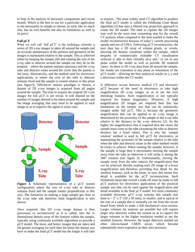
Full µCT
What we will call ‘full µCT’ is the technique whereby a
series of 2D x-ray images is taken all around the sample and
an accurate maintenance of the position and geometry of the
images is maintained relative to the sample. This is achieved
either by keeping the sample still and rotating the axis of the
x-ray tube to detector around the sample (as they do in the
hospital - where the patient remains stationary and the x-ray
tube and detector rotate around the circle that the patient is
fed into). Alternatively, and the method used for electronics
applications, is where the axis of the tube to detector
remains fixed and the sample is rotated relative to this plane
(see figure3). Whichever motion paradigm is chosen, a
dataset of 2D x-ray images is acquired from all angles
around the sample. The time to acquire the original 2D x-ray
images for full µCT is not trivial. It will depend on the
number of images desired to be taken around the sample and
the image averaging that may need to be applied to each
image so as to improve the signal to noise ratio.
Figure 3. Schematic representation of a µCT system
configuration where the axis of x-ray tube to detector
remains fixed and the sample rotates perpendicular to this
axis. The limitation on making a large sample get close to
the x-ray tube and therefore limit magnification is also
shown.
Once acquired, this 2D x-ray image dataset is then
processed, or reconstructed as it is called, into the 3-
dimensional density array of the features within the sample,
typically using commonly available algorithms to provide a
µCT model. The more, and better, images that are taken and
the greater averaging for each then the better the dataset you
have to make the final µCT model but the longer it will take
to acquire. The most widely used CT algorithm to produce
the final µCT model is called the Feldkamp Cone Beam
algorithm [3] that uses a filtered rear projection approach to
create the 3D model. The time to capture the 2D images
may well be the most time consuming step for the overall
CT analysis when compared to the time needed to make the
model reconstruction because of today’s current processing
speeds and use of GPUs. Following µCT reconstruction, the
user then has a 3D array of volume pixels, or voxels,
showing the density variations within the sample, which
bespoke or commercially available CT visualisation
software is able to then virtually slice and / or cut in any
plane within the model as well as provide 3D rendered
views. As there is 2D x-ray data from all around the sample,
the results are consistent in any plane or orientation of the
µCT model – allowing the best analytical results in x, y and
z directions within the CT model.
A difference occurs between medical CT and electronic
µCT because of the need in electronics to take high
magnification 2D x-ray images so as to see the ever
shrinking features. Such magnification is not typically
required for human diagnostics. However, if high
magnification 2D images are required then this has
limitations on the sample size that can be realistically
imaged under full µCT. This is because the geometric
magnification that can be applied to an x-ray image is
determined by the proximity of the sample to the x-ray tube
relative to the distance to the x-ray detector [2]. So the
higher the magnification that is required then the closer the
sample must come to the tube (assuming the tube to detector
distance has a fixed value). This is why the ‘sample
rotation’ method is used in full µCT for electronics, as
maintaining the proximity of the sample relative to the tube
when the tube and detector rotate in the other method would
be tricky to achieve. When rotating the sample, however, if
the sample is large then it necessitates moving the sample
away from the tube as otherwise it will strike it during the
360° rotation (see figure 3). Unfortunately, moving the
sample away from the tube reduces the magnification that
can be achieved, thereby making each 2D image of a lower
magnification and therefore providing less detail for the
smallest features, such as the joints. In turn, this means less
detail is available for the µCT reconstruction. Such
limitations mean that overall a trade off must be made in full
µCT analysis for electronics applications of the practical
sample size that can be used against the magnification and
detail available in the final µCT model. For most commonly
available electronic µCT x-ray systems this sample size
limit is ~ 2” x 2” (50 x 50 mm), or smaller, and is typical of
the size of a sample that is normally cut out from the circuit
board from which to make a full mechanical cross-section.
Larger volumes for analysis are possible but will require
larger area detectors within the system so as to capture the
larger volumes in the higher resolution needed to see the
smallest features. However, the larger detectors needed are
often silicon-based CMOS arrays which become
substantially more expensive as their area increases.
Therefore, using full µCT to inspect PCB electronics can be
considered as an optimum technique ahead of making a full
mechanical cross-section, where the sample has already
been cut out of the board and allows a 3D model to be made
in minutes that will permit virtual cross-sectioning
anywhere within the model. Whilst the µCT data will not
have the same resolution as that seen in a SEM, the virtual
cross-sections in µCT are available in a fraction of the time
that it will take to allow for the epoxy to harden and then
polish the sample, as is necessary for the mechanical cross-
section technique. In addition, the µCT technique does not
introduce additional mechanical defects within the sample
volume, which is always a concern with mechanical cross
sectioning. At best, full µCT will show the flaws in the
sample quickly and reduce, or completely eliminate, the
number of mechanical cross-sections that have to be taken.
At worst, it will identify to the user where the polishing of
the cross-section must be made such that an over-polish will
not destroy the exact location that needs to be viewed.
Overall, full µCT provides the optimum analytical
information for electronics applications using the CT
technique but unless the whole sample is very small, it will
require destruction of the original sample in order that there
is sufficient resolution in the final µCT model to make the
necessary analysis.
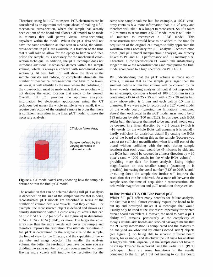
Figure 4. CT model voxel array showing how the sample is
defined within the final µCT model.
The resolution that can be achieved during full µCT analysis
is dependent on the size of the sample volume that is being
reconstructed. µCT models are described in terms of the
number of volume pixels or ‘voxels’ that they contain. For
example, the reconstructed object is defined and shown as a
density distribution within a cubic array of voxels that can
be 512 x 512 x 512 (or 5123 - see figure 4) in dimension,
1024 x 1024 x 1024 (10243), or more. The larger the voxel
array size then the more voxels will cover the sample and
therefore improve the resolution. The ultimate resolution in
full µCT is determined by the original size of the sample,
the field of view for the CT scan, and the capability of the x-
ray tube and image detector. The smaller the analysis
volume, the better the resolution you have because you are
dividing the same number of voxels over a smaller volume.
Having more voxels will improve the resolution for the
same size sample volume but, for example, a 10243 voxel
array contains 8 X more information than a 5123 array and
therefore will take ~ 8 X longer to reconstruct. So, if it takes
~ 2 minutes to reconstruct a 5123 model then it will take ~
16 minutes to reconstruct a 10243 model. This
reconstruction time would have to be added to the time for
acquisition of the original 2D images to fully appreciate the
workflow times necessary for µCT analysis. Reconstruction
times (and µCT model manipulation / analysis) are directly
linked to PC and GPU performance and PC memory size.
Therefore, a low specification PC would take substantially
longer to make the reconstructions (and manipulate the final
model) compared to a high specification PC / GPU.
By understanding that the µCT volume is made up of
voxels, it means that as the sample gets larger then the
smallest details within that volume will be covered by far
fewer voxels - making analysis difficult if not impossible.
As an example, consider a board of 100 x 100 mm in size
containing a BGA of 25 x 25 mm with a 20 x 20 solder ball
array whose pitch is 1 mm and each ball is 0.5 mm in
diameter. If we were able to reconstruct a 5123 voxel model
of the whole board (ignoring the limitations mentioned
above) then each voxel in the µCT model array would be of
195 microns by side (100 mm/512). In this case, each BGA
solder ball, the features that need to be analysed, would only
be covered in a linear direction by ~ 2.5 voxels (which is
~16 voxels for the whole BGA ball assuming it is round) -
hardly sufficient for analytical detail! By cutting the BGA
out of the board and using this as the sample (because you
cannot get sufficient magnification when it is still part of the
board without colliding with the tube during sample
rotation) then each voxel would be 49 microns by side and
the BGA ball would be covered in a linear direction by ~ 10
voxels (and ~ 1000 voxels for the whole BGA volume) –
providing more data for better analysis. Using higher
magnification on this smaller sample (assuming it is
possible), increasing the voxel number (5123 to 2048
3), and /
or cutting down the sample size further will improve the
resolution that can be achieved. So a trade-off between the
sample size, the time of acquisition / reconstruction, the
achievable magnification and µCT resolution always exists.
In-line Partial CT & Off-Line Partial µCT
Whilst full µCT offers many benefits for failure analysis,
the fact that it will almost certainly require the board to be
cut up and destroyed makes it a technique that would
usually only be used at the last resort, especially for printed
circuit board assemblers. However, the need to have a µCT
ability still remains, particularly as the complexity of
today’s double-side boards and stacked packages means that
the 2D x-ray information is complicated and the features to
be analysed are obscured by other (second side?) objects
(see figure 1). So being able to separate different board
layers, for example, and de-clutter the 2D view for analysis
is highly desirable, especially if the sample does not have to
be cut up. This can be achieved using the Partial µCT (PCT)
technique. There are some limitations in the results
compared to the full µCT but not having to cut the board
makes it most attractive for PCB electronic applications
before taking more drastic action.
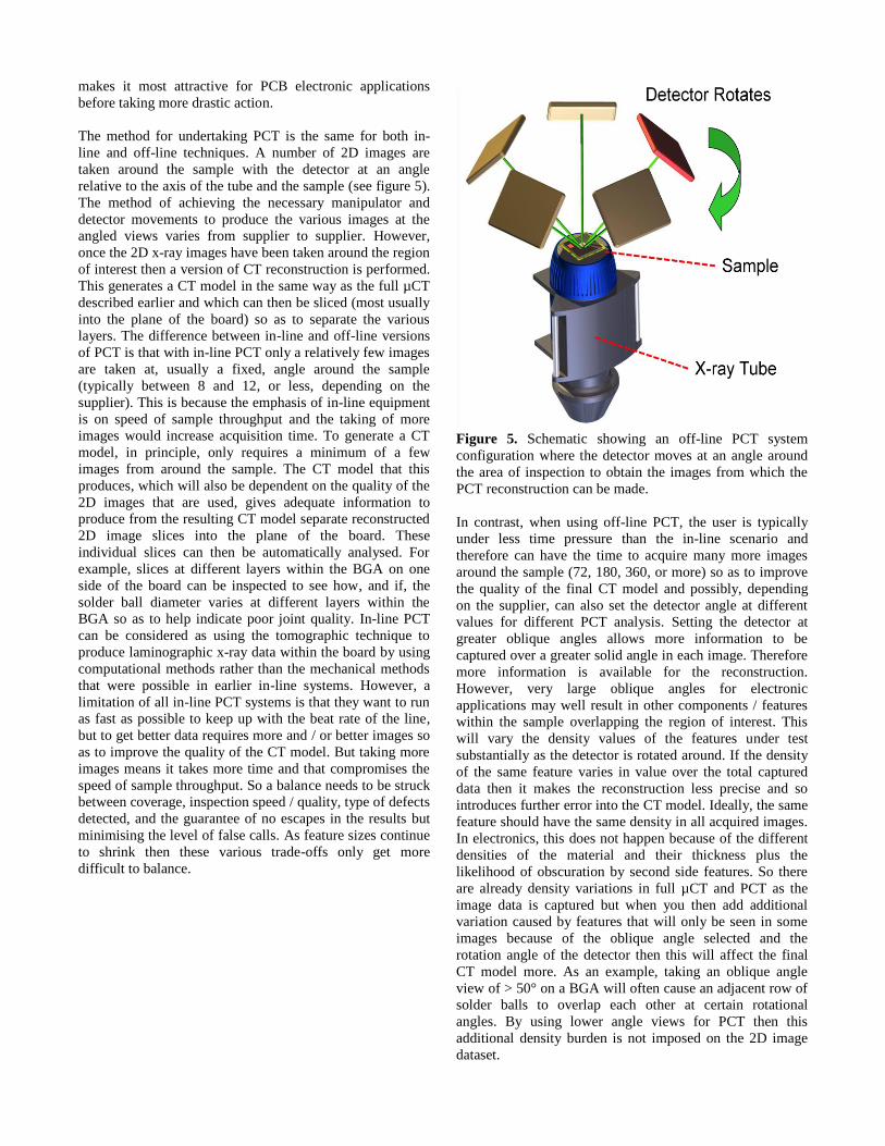
The method for undertaking PCT is the same for both in-
line and off-line techniques. A number of 2D images are
taken around the sample with the detector at an angle
relative to the axis of the tube and the sample (see figure 5).
The method of achieving the necessary manipulator and
detector movements to produce the various images at the
angled views varies from supplier to supplier. However,
once the 2D x-ray images have been taken around the region
of interest then a version of CT reconstruction is performed.
This generates a CT model in the same way as the full µCT
described earlier and which can then be sliced (most usually
into the plane of the board) so as to separate the various
layers. The difference between in-line and off-line versions
of PCT is that with in-line PCT only a relatively few images
are taken at, usually a fixed, angle around the sample
(typically between 8 and 12, or less, depending on the
supplier). This is because the emphasis of in-line equipment
is on speed of sample throughput and the taking of more
images would increase acquisition time. To generate a CT
model, in principle, only requires a minimum of a few
images from around the sample. The CT model that this
produces, which will also be dependent on the quality of the
2D images that are used, gives adequate information to
produce from the resulting CT model separate reconstructed
2D image slices into the plane of the board. These
individual slices can then be automatically analysed. For
example, slices at different layers within the BGA on one
side of the board can be inspected to see how, and if, the
solder ball diameter varies at different layers within the
BGA so as to help indicate poor joint quality. In-line PCT
can be considered as using the tomographic technique to
produce laminographic x-ray data within the board by using
computational methods rather than the mechanical methods
that were possible in earlier in-line systems. However, a
limitation of all in-line PCT systems is that they want to run
as fast as possible to keep up with the beat rate of the line,
but to get better data requires more and / or better images so
as to improve the quality of the CT model. But taking more
images means it takes more time and that compromises the
speed of sample throughput. So a balance needs to be struck
between coverage, inspection speed / quality, type of defects
detected, and the guarantee of no escapes in the results but
minimising the level of false calls. As feature sizes continue
to shrink then these various trade-offs only get more
difficult to balance.
Figure 5. Schematic showing an off-line PCT system
configuration where the detector moves at an angle around
the area of inspection to obtain the images from which the
PCT reconstruction can be made.
In contrast, when using off-line PCT, the user is typically
under less time pressure than the in-line scenario and
therefore can have the time to acquire many more images
around the sample (72, 180, 360, or more) so as to improve
the quality of the final CT model and possibly, depending
on the supplier, can also set the detector angle at different
values for different PCT analysis. Setting the detector at
greater oblique angles allows more information to be
captured over a greater solid angle in each image. Therefore
more information is available for the reconstruction.
However, very large oblique angles for electronic
applications may well result in other components / features
within the sample overlapping the region of interest. This
will vary the density values of the features under test
substantially as the detector is rotated around. If the density
of the same feature varies in value over the total captured
data then it makes the reconstruction less precise and so
introduces further error into the CT model. Ideally, the same
feature should have the same density in all acquired images.
In electronics, this does not happen because of the different
densities of the material and their thickness plus the
likelihood of obscuration by second side features. So there
are already density variations in full µCT and PCT as the
image data is captured but when you then add additional
variation caused by features that will only be seen in some
images because of the oblique angle selected and the
rotation angle of the detector then this will affect the final
CT model more. As an example, taking an oblique angle
view of > 50° on a BGA will often cause an adjacent row of
solder balls to overlap each other at certain rotational
angles. By using lower angle views for PCT then this
additional density burden is not imposed on the 2D image
dataset.
A further advantage of off-line PCT is that it possible to
concentrate on a smaller area / volume of inspection
compared to in-line and full µCT approaches. This is
because the magnification is not limited compared to full
µCT, as the sample can always be placed as close as
possible to the x-ray tube and does not rotate into the tube.
With in-line PCT, although the magnification could and can
be increased, the result is that many more inspection points
need to be made to cover the same inspection area as when
using lower magnifications and therefore will substantially
increase the inspection time, something that may be
unacceptable for the beat rate to the manufacturing line.
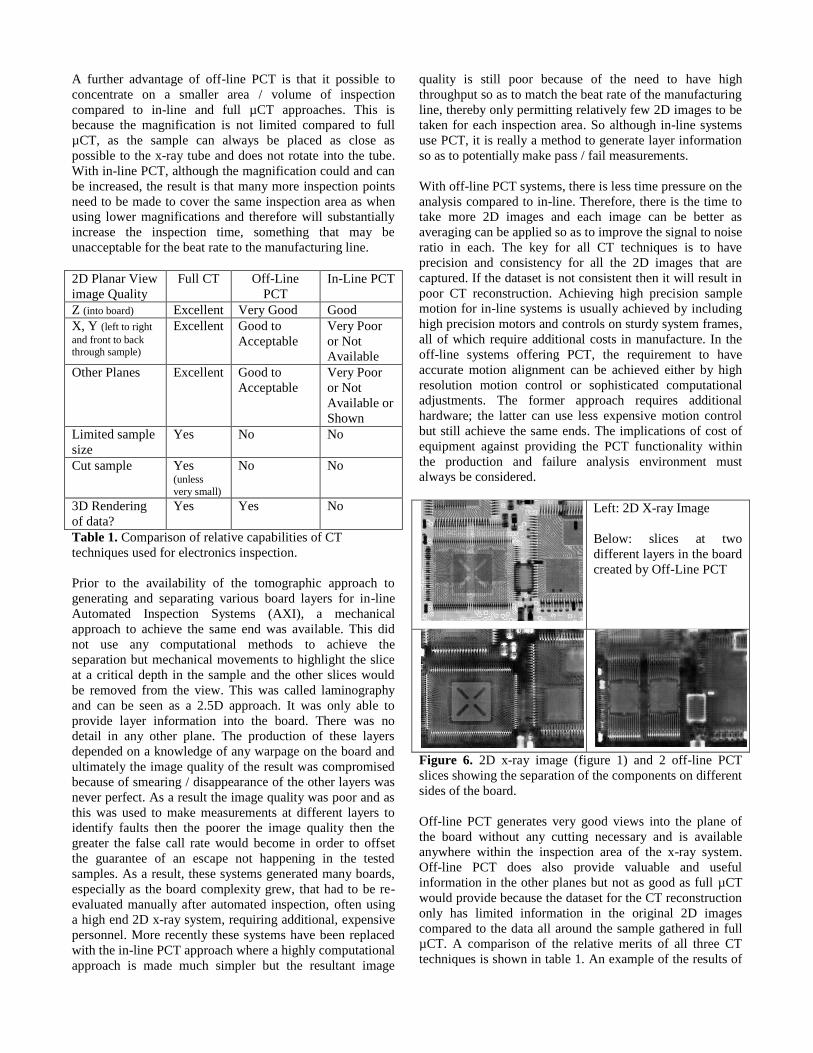
2D Planar View
image Quality
Full CT Off-Line
PCT
In-Line PCT
Z (into board) Excellent Very Good Good
X, Y (left to right
and front to back through sample)
Excellent Good to
Acceptable
Very Poor
or Not
Available
Other Planes Excellent Good to
Acceptable
Very Poor
or Not
Available or
Shown
Limited sample
size
Yes No No
Cut sample Yes (unless
very small)
No No
3D Rendering
of data?
Yes Yes No
Table 1. Comparison of relative capabilities of CT
techniques used for electronics inspection.
Prior to the availability of the tomographic approach to
generating and separating various board layers for in-line
Automated Inspection Systems (AXI), a mechanical
approach to achieve the same end was available. This did
not use any computational methods to achieve the
separation but mechanical movements to highlight the slice
at a critical depth in the sample and the other slices would
be removed from the view. This was called laminography
and can be seen as a 2.5D approach. It was only able to
provide layer information into the board. There was no
detail in any other plane. The production of these layers
depended on a knowledge of any warpage on the board and
ultimately the image quality of the result was compromised
because of smearing / disappearance of the other layers was
never perfect. As a result the image quality was poor and as
this was used to make measurements at different layers to
identify faults then the poorer the image quality then the
greater the false call rate would become in order to offset
the guarantee of an escape not happening in the tested
samples. As a result, these systems generated many boards,
especially as the board complexity grew, that had to be re-
evaluated manually after automated inspection, often using
a high end 2D x-ray system, requiring additional, expensive
personnel. More recently these systems have been replaced
with the in-line PCT approach where a highly computational
approach is made much simpler but the resultant image
quality is still poor because of the need to have high
throughput so as to match the beat rate of the manufacturing
line, thereby only permitting relatively few 2D images to be
taken for each inspection area. So although in-line systems
use PCT, it is really a method to generate layer information
so as to potentially make pass / fail measurements.
With off-line PCT systems, there is less time pressure on the
analysis compared to in-line. Therefore, there is the time to
take more 2D images and each image can be better as
averaging can be applied so as to improve the signal to noise
ratio in each. The key for all CT techniques is to have
precision and consistency for all the 2D images that are
captured. If the dataset is not consistent then it will result in
poor CT reconstruction. Achieving high precision sample
motion for in-line systems is usually achieved by including
high precision motors and controls on sturdy system frames,
all of which require additional costs in manufacture. In the
off-line systems offering PCT, the requirement to have
accurate motion alignment can be achieved either by high
resolution motion control or sophisticated computational
adjustments. The former approach requires additional
hardware; the latter can use less expensive motion control
but still achieve the same ends. The implications of cost of
equipment against providing the PCT functionality within
the production and failure analysis environment must
always be considered.
Left: 2D X-ray Image
Below: slices at two
different layers in the board
created by Off-Line PCT
Figure 6. 2D x-ray image (figure 1) and 2 off-line PCT
slices showing the separation of the components on different
sides of the board.
Off-line PCT generates very good views into the plane of
the board without any cutting necessary and is available
anywhere within the inspection area of the x-ray system.
Off-line PCT does also provide valuable and useful
information in the other planes but not as good as full µCT
would provide because the dataset for the CT reconstruction
only has limited information in the original 2D images
compared to the data all around the sample gathered in full
µCT. A comparison of the relative merits of all three CT
techniques is shown in table 1. An example of the results of
an off-line PCT examination is shown is figure 6, where
slices at two separate layers into the board (figure 1) are
shown so that the different components on the different
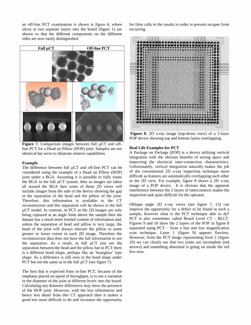
sides are now easily distinguished.
Full µCT Off-line PCT
Figure 7. Comparison images between full µCT and off-
line PCT for a Head on Pillow (HOP) joint. Samples are not
identical but serve to illustrate relative capabilities.
Example
The difference between full µCT and off-line PCT can be
considered using the example of a Head on Pillow (HOP)
joint under a BGA. Assuming it is possible to fully rotate
the BGA in the full µCT system, then as images are taken
all around the BGA then some of those 2D views will
include images from the side of the device showing the gap
in the separation of the head and the pillow of the joint.
Therefore, this information is available to the CT
reconstruction and this separation will be shown in the full
µCT model. In contrast, in PCT as the 2D images are only
being captured at an angle from above the sample then the
dataset has a much more limited content of information and,
unless the separation of head and pillow is very large, the
head of the joint will always obscure the pillow to some
greater or lesser extent in each 2D image. Therefore the
reconstruction data does not have the full information to see
the separation. As a result, in full µCT you see the
separation between the head and the pillow but in PCT there
is a different bond shape, perhaps like an ‘hourglass’ type
shape. So a difference is still seen in the bond shape under
PCT but not the same as in the full µCT (see figure 7).
The best that is expected from in-line PCT, because of the
emphasis placed on speed of throughput, is to see a variation
in the diameter of the joint at different levels into the board.
Calculating any diameter differences may show the presence
of the HOP joint. However, with the less information and
hence less detail from this CT approach then it makes a
good test more difficult to do and increases the opportunity
for false calls in the results in order to prevent escapes from
occurring.
Figure 8. 2D x-ray image (top-down view) of a 2-layer
POP device showing top and bottom layers overlapping.
Real Life Examples for PCT
A Package on Package (POP) is a device utilizing vertical
integration with the obvious benefits of saving space and
improving the electrical inter-connection characteristics.
Unfortunately, vertical integration naturally makes the job
of the conventional 2D x-ray inspection technique more
difficult as features are automatically overlapping each other
in the 2D view. For example, figure 8 shows a 2D x-ray
image of a POP device. It is obvious that the apparent
interference between the 2 layers of interconnects makes the
inspection task quite difficult for the operator.
Oblique angle 2D x-ray views (see figure 7, 13) can
improve the opportunity for a defect to be found in such a
sample, however what is the PCT technique able to do?
PCT is also sometimes called Board Level CT - BLCT.
Figures 9 and 10 show the 2 layers of the POP in figure 8
separated using PCT – from a fast and low magnification
scan technique. Layer 1 (figure 9) appears flawless.
However, from the PCT image representing level 2 (figure
10) we can clearly see that two joints are incomplete (red
arrows) and something abnormal is going on inside the red
box area.
Figure 9. Fast, low magnification PCT scan of POP device
in figure 8. The virtual cross section through the plane of
layer 1 looks consistent and good.
Figure10. Fast, low magnification PCT scan of the POP
device in figure 8. Virtual cross section through Layer 2
shows incomplete / open joints (red arrows) and abnormal
joints (red square).
The missing / open joints are obvious (red arrows in figure
10). However, the next step is to do a fast PCT scan at
higher magnification concentrating on the area within the
red box of Figure 10. The results are presented in Figure 11,
which shows virtual cross sections through the suspected
joints in (a) a vertical plane, (b) a horizontal plane and (c) a
3D rendered view of the CT model. It is obvious the joints
in the red box did not reflow properly, resulting in open, or
intermittent connections.
Figure 11. PCT scan of the area within the red box in
Figure 10. a) Virtual cross section through a vertical plane,
b) virtual cross section in horizontal plane through the open
/ intermittent joints, (c) 3D rendered view of CT model.
Intermittent connections can be even more devastating as
the device could pass the electrical tests and end up failing
in the field. The possible cause for these defects is
contamination of the package / PCB or deposition of an
incorrect amount of paste.
Figure 12 is another example of a defect that is very
difficult, or impossible, to diagnose just using 2D x-ray /
oblique angle techniques. The bottom layer of the POP
device (rendered in gold) looks fine. The joints of the top
layer (rendered in red) are angled away from the lower layer
with the angle increasing towards the outside of the
package. The reason behind this fault could be mismatch
and / or package warping.
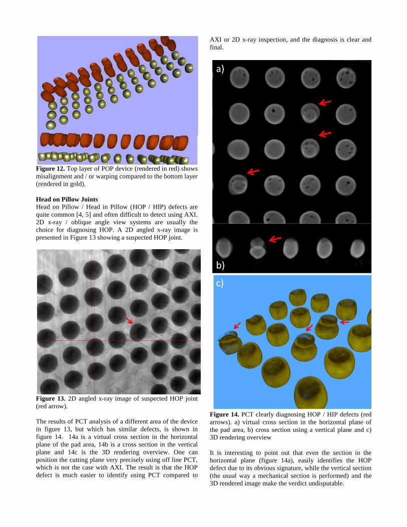
Figure 12. Top layer of POP device (rendered in red) shows
misalignment and / or warping compared to the bottom layer
(rendered in gold).
Head on Pillow Joints
Head on Pillow / Head in Pillow (HOP / HIP) defects are
quite common [4, 5] and often difficult to detect using AXI.
2D x-ray / oblique angle view systems are usually the
choice for diagnosing HOP. A 2D angled x-ray image is
presented in Figure 13 showing a suspected HOP joint.
Figure 13. 2D angled x-ray image of suspected HOP joint
(red arrow).
The results of PCT analysis of a different area of the device
in figure 13, but which has similar defects, is shown in
figure 14. 14a is a virtual cross section in the horizontal
plane of the pad area, 14b is a cross section in the vertical
plane and 14c is the 3D rendering overview. One can
position the cutting plane very precisely using off line PCT,
which is not the case with AXI. The result is that the HOP
defect is much easier to identify using PCT compared to
AXI or 2D x-ray inspection, and the diagnosis is clear and
final.
Figure 14. PCT clearly diagnosing HOP / HIP defects (red
arrows). a) virtual cross section in the horizontal plane of
the pad area, b) cross section using a vertical plane and c)
3D rendering overview
It is interesting to point out that even the section in the
horizontal plane (figure 14a), easily identifies the HOP
defect due to its obvious signature, while the vertical section
(the usual way a mechanical section is performed) and the
3D rendered image make the verdict undisputable.

Figure 15. PCT showing HOP / HIP defects second
example. a) virtual cross section in the horizontal plane of
the pad area, b) cross section using a vertical plane and c)
3D rendering overview
Figure 15 shows another example of HOP defect for a
different device. Again the diagnosis is very fast and
convincing.
Connectors
Verifying how well a complex connector is engaged /
soldered within the assembled product has always been a
challenge. Historically, the only way to confirm this was to
mechanically cut the board / assembly, which results in
destroying the expensive assembled product. The full µCT
option is also destructive in this case, as usually the
connector is mounted on a large board within a large
assembly, and the only way to do a CT scan and get
reasonable data with useful resolution is to cut the connector
out of the board. Undertaking 2D x-ray is also not practical
as the 2D image is very complex, and can be cluttered with
all the other parts surrounding the connector in question, as
shown in Figure 16. Figure 16 shows how it is very
difficult, or impossible, to verify how well a connector
engages using the standard 2D x-ray technique even with
oblique angle viewing. For this particular example, we are
showing an entire smart phone assembly.
Figure 16. Angled 2D x-ray view of a connector within a
smart phone assembly. The connector is in the area marked
by the red box. Correct engagement cannot be verified even
using multiple viewing angles and higher magnification.
In Figure 17, we show virtual cross sections of the same
connector in figure 16, produced by PCT, while keeping the
whole assembly (smart phone) intact. Figure 17a is a section
in the horizontal plane and Figure 17b is a section in the
vertical plane.
Figure 17. PCT virtual cross sections of a connector within
a smart phone assembly. a) section in the horizontal plane,
b) section in the vertical plane. Satisfactory engagement is
verified in the areas shown by the yellow arrows.

The PCT scan resulted in eliminating the clutter evident in
the 2D images. Using virtual cross sectioning in the right
locations clearly shows that satisfactory engagement of the
connector took place at the areas indicated by the yellow
arrows. Confidence of this result is even higher as the
phone worked before placement in the x-ray machine!
Figure 18. PCT of 100 micron diameter bump interconnects
showing cracks resulting in the bump being split in half (red
arrow). The blue lines point towards interfacial voiding.
Figure 19. PCT 3D model of a QFN device. Extremely
large void is shown going through the whole solder joint -
suspected in overview (a) and confirmed in section view (b).
Solder Bumps
While PCT was developed mainly as a PCB inspection
technique, it has been found to be very useful as a 3D non-
destructive method for examining micro bumps on a wafer
or package level. Wafer bumps are getting smaller and
smaller with 20 - 30 micron diameter bumps not uncommon
today. Figure 18 shows a PCT of a micro-bump sample. The
red arrow points to a crack defect in a bump which has
resulted in the bump in question being split in half. The
blue arrows show some interfacial voiding, which could also
pose a future problem by reducing the possible joint
reliability.
Area Voids A PCT model of a QFN device is shown in Figure 19,
where 19a represents a section overview of the whole QFN
device. The joint marked with the red arrow demonstrates
an extremely large void apparently going through the whole
solder joint. This is confirmed by Figure 19b which is a
section through the joint in question, as well as its
neighbours. This extremely large void makes the solder joint
very unreliable and likely open or intermittent in function.
Precise locating of voiding positions is a known strength of
the CT technique and nicely demonstrated here with this
PCT case.
Figure 20. PCT 3D rendered model of a QFN device
showing insufficient joints (red arrows). The solder
thickness is also able to be measured in the rendered view.
In Figure 20, we have the same QFN device seen in figure
19 but shown at an angled PCT section overview. The
solder joints indicated with the red arrows are clearly
insufficient when compared with their neighbours. In
addition, figure 20 demonstrates a very important additional
feature that is available - measurement capabilities such as
that of solder thickness as well as volumetric information
pertinent to the solder joint – i.e. solder and voiding
volumes. Thus the PCT technique lets us not only examine
in detail the solder shape and variation but also can produce
very important numerical data.
CONCLUSION In this paper we have discussed the various CT techniques
that are available for electronics inspection including the
off-line partial µCT (PCT) technique, also known as board
level CT. This comparatively novel technique presents us

with the capability of creating, in a short time, very
reasonable quality 3D CT models of areas within large
PCBs or other electronics assemblies. This is achieved in a
completely non-destructive fashion, something that is not
usually true when full µCT is undertaken. The PCT
technique has been illustrated using a wide variety of
examples of SMT devices that have included real life
defects. By producing non-destructive defect diagnosis in a
fast and convincing manner through virtual cross sections of
samples, this makes PCT a powerful alternative / precursor
to mechanical cross sectioning. In addition linear
measurement and volumetric data are readily available, thus
providing important quantitative data to be added to the
qualitative analysis.
ACKNOWLEDEMENTS
The authors would like to thank Derren Felgate and Vineeth
Bastin for great help with this paper.
REFERENCES
[1] ‘Considerations for Minimizing Radiation Doses to
Components during X-ray Inspection’, D. Bernard & R.
Blish II, Proceedings of SMTAI, 2003
[2] ‘Selection Criteria for X-ray Inspection
Systems for BGA and CSP Solder Joint Analysis’, D.
Bernard, Proceedings of Nepcon Shanghai, 2003
[3] ‘Practical Cone-Beam Algorithm’, L. A. Feldkamp, L.
C. Davis, and J. W. Kress, J. Opt. Soc. Am. A/Vol. 1,
No. 6, June 1984
[4] ‘A Practical Guide to X-ray Inspection Criteria &
Common Defect Analysis’, D. Bernard & B. Willis, Dage
Publications 2006, available through the SMTA bookshop
[5] ‘Modern 2d / 3d X-ray Inspection - Emphasis on BGA,
QFN, 3d Packages, and Counterfeit Components’,
E.Krastev & D. Bernard, Pan Pacific Symposium
Conference Proceedings 2010, available through the SMTA
bookshop
Originally published in the Proceedings of the SMTA
International Conference, Orlando, Florida, October 14 –
28, 2012