3d charge trapping (ct) nand flash - sematech charge trapping (ct) nand flash. 2 outline why does...
TRANSCRIPT
1
Yen-Hao Shih
Macronix International Co., Ltd.Macronix International Co., Ltd.HsinchuHsinchu, Taiwan, Taiwan
Email: Email: [email protected]@mxic.com.tw
3D Charge Trapping (CT) NAND Flash
2
Outline
� Why Does NAND Go to 3D?
� Design a 3D NAND Flash Memory
� Challenges and Opportunities in 3D CT NAND Flash Memory
� Summary
3
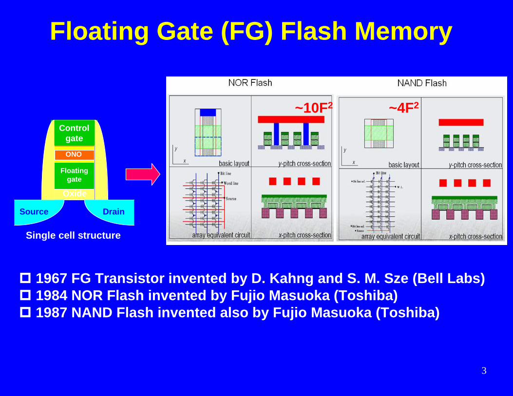
Floating Gate (FG) Flash Memory
Source
Oxide
Floating gate
Control gate
Drain
Single cell structure
ONO
~4F2~10F2
� 1967 FG Transistor invented by D. Kahng and S. M. Sz e (Bell Labs)� 1984 NOR Flash invented by Fujio Masuoka (Toshiba)� 1987 NAND Flash invented also by Fujio Masuoka (Toshi ba)
4
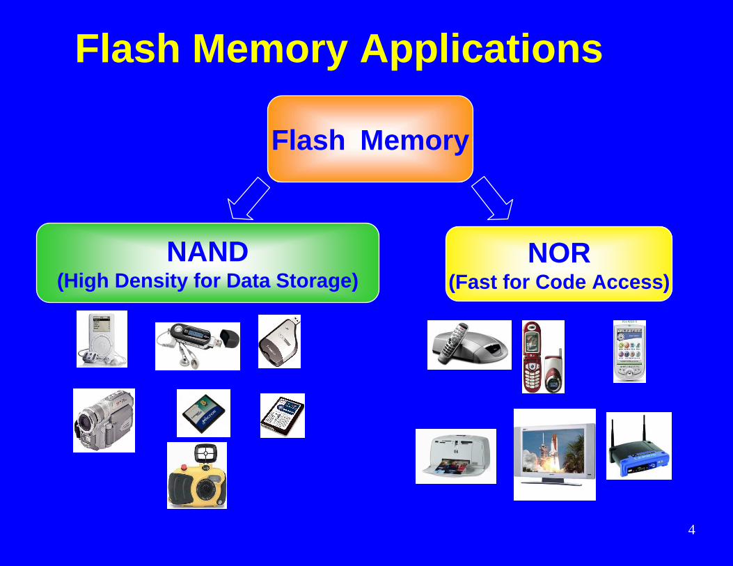
Flash Memory
NOR(Fast for Code Access)
NAND(High Density for Data Storage)
Flash Memory Applications
5
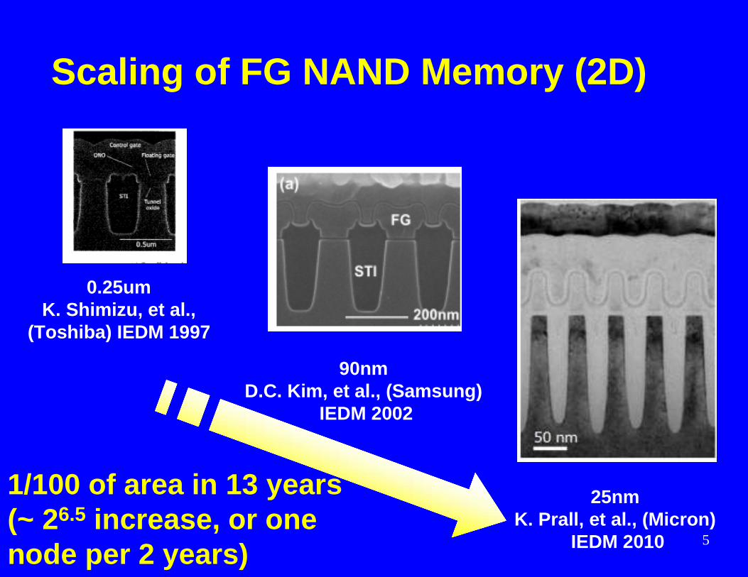
Scaling of FG NAND Memory (2D)
90nm D.C. Kim, et al., (Samsung)
IEDM 2002
0.25umK. Shimizu, et al.,
(Toshiba) IEDM 1997
25nm K. Prall, et al., (Micron)
IEDM 2010
1/100 of area in 13 years(~ 26.5 increase, or one node per 2 years)
6
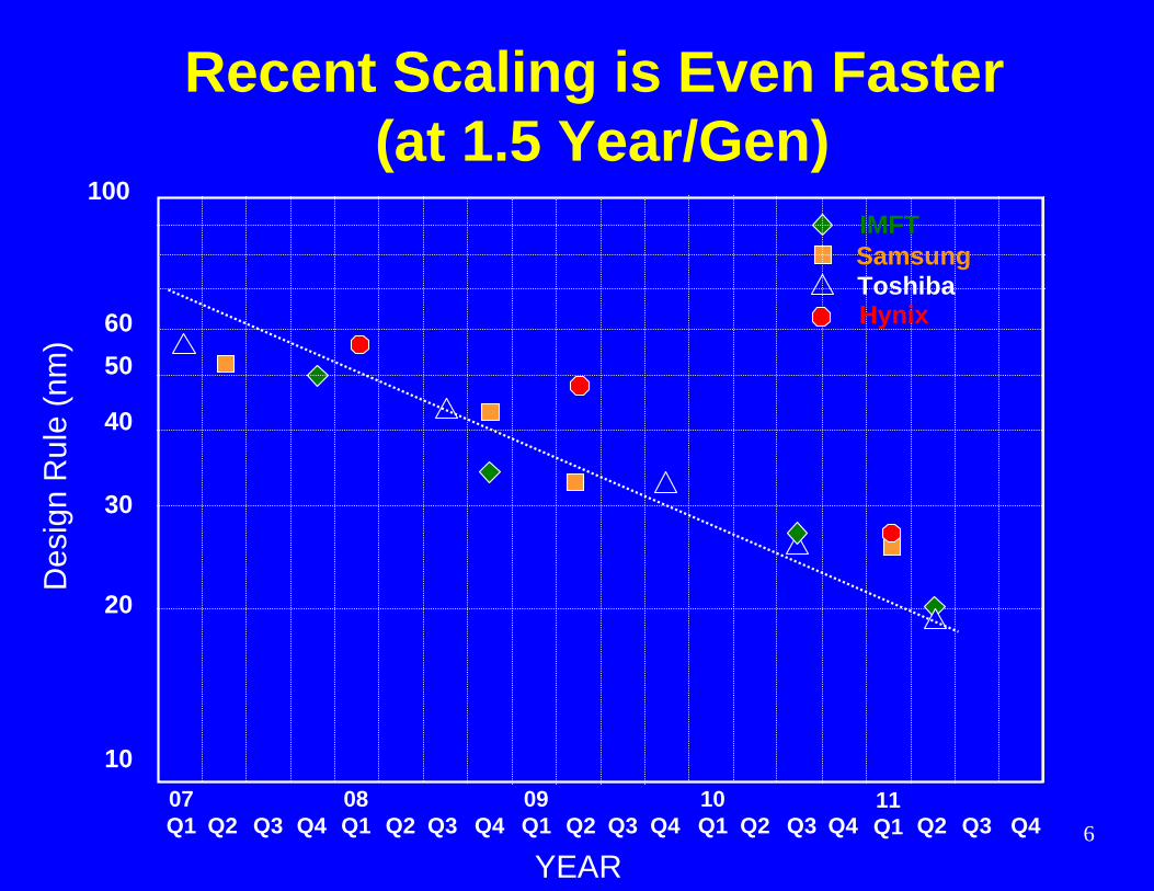
Recent Scaling is Even Faster(at 1.5 Year/Gen)
YEAR
100
10
20
30
40
50
60
07Q1 Q2 Q3 Q4
08Q1 Q2 Q3 Q4
09Q1 Q2 Q3 Q4
10Q1 Q2 Q3 Q4
11Q1 Q2 Q3 Q4
IMFTSamsungToshibaHynix
Des
ign
Rul
e (n
m)
7
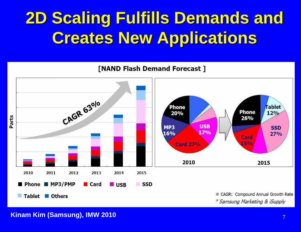
2D Scaling Fulfills Demands and 2D Scaling Fulfills Demands and Creates New Applications Creates New Applications
Kinam Kim (Samsung), IMW 2010
8
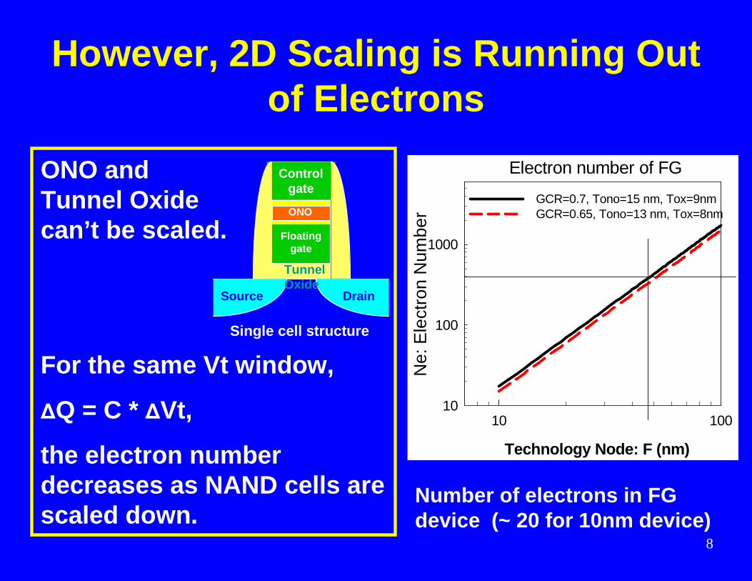
However, 2D Scaling is Running Out of Electrons
Number of electrons in FG device (~ 20 for 10nm device)
ONO and Tunnel Oxidecan’t be scaled.
For the same Vt window,
∆Q = C * ∆Vt,
the electron number decreases as NAND cells are scaled down.
Electron number of FG
Technology Node: F (nm)
10 100N
e: E
lect
ron
Num
ber
10
100
1000
GCR=0.7, Tono=15 nm, Tox=9nmGCR=0.65, Tono=13 nm, Tox=8nm
Source
Tunnel Oxide
Floating gate
Control gate
Drain
Single cell structure
ONO
9
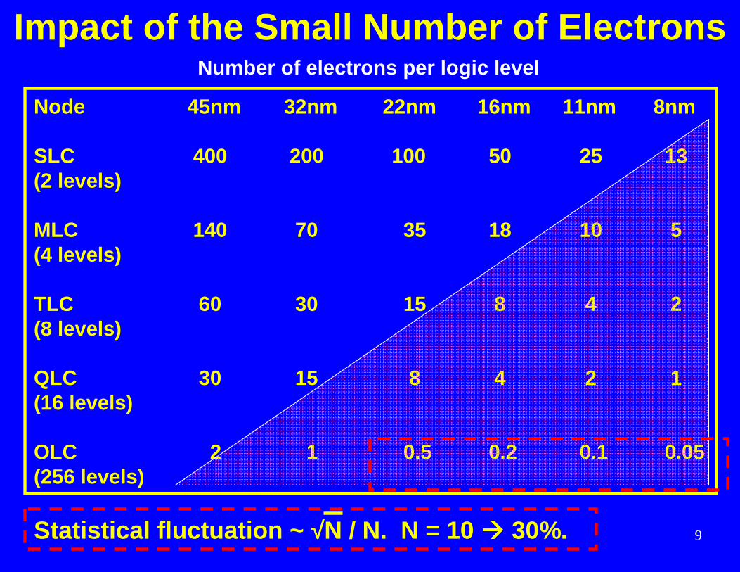
Impact of the Small Number of ElectronsNumber of electrons per logic level
Node 45nm 32nm 22nm 16nm 11nm 8nm
SLC 400 200 100 50 25 13(2 levels)
MLC 140 70 35 18 10 5(4 levels)
TLC 60 30 15 8 4 2(8 levels)
QLC 30 15 8 4 2 1(16 levels)
OLC 2 1 0.5 0.2 0.1 0.05(256 levels)
Statistical fluctuation ~ √√√√N / N. N = 10 ���� 30%.
10
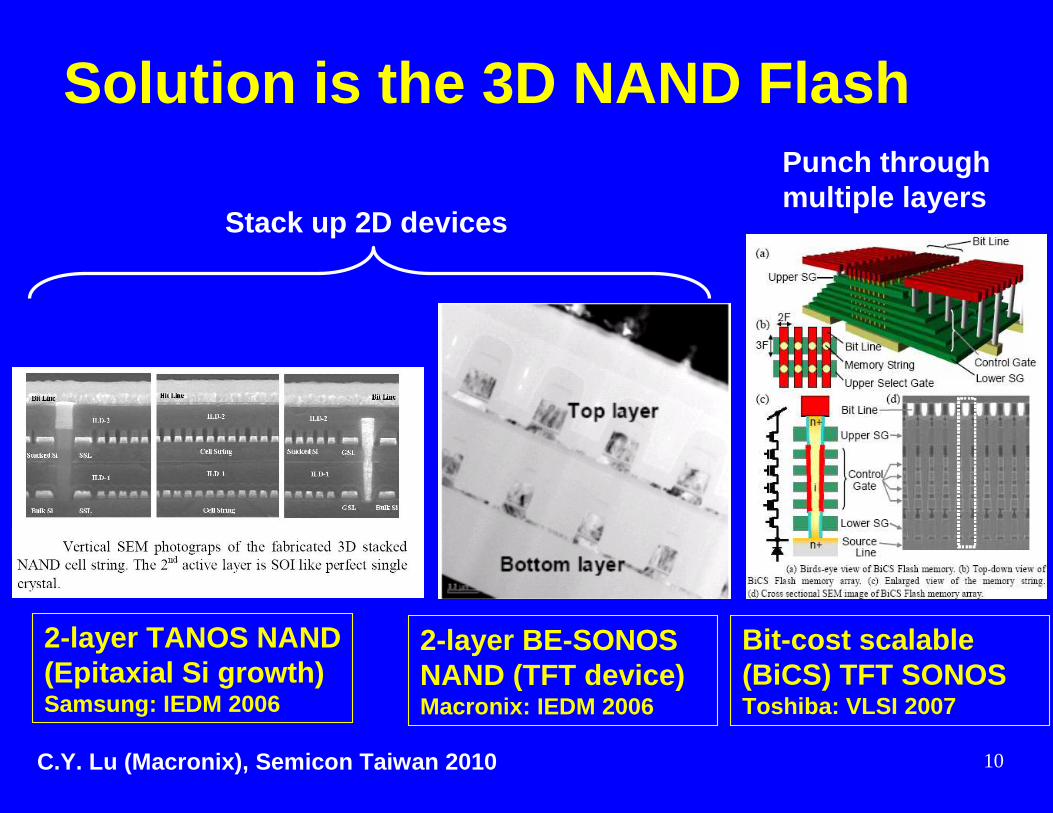
Solution is the 3D NAND Flash
Stack up 2D devices
Punch through multiple layers
2-layer TANOS NAND(Epitaxial Si growth)Samsung: IEDM 2006
2-layer BE-SONOS NAND (TFT device)Macronix: IEDM 2006
Bit-cost scalable (BiCS) TFT SONOSToshiba: VLSI 2007
C.Y. Lu (Macronix), Semicon Taiwan 2010
11
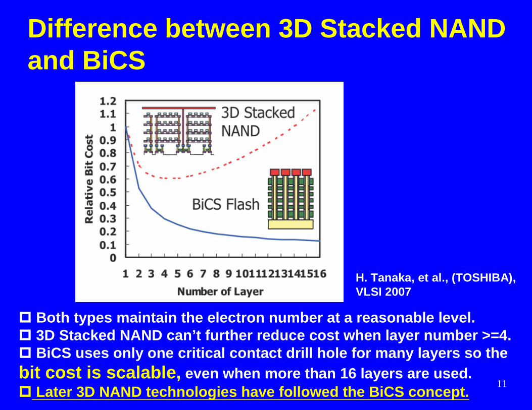
Difference between 3D Stacked NANDand BiCS
H. Tanaka, et al., (TOSHIBA), VLSI 2007
� Both types maintain the electron number at a reason able level.� 3D Stacked NAND can’t further reduce cost when laye r number >=4.� BiCS uses only one critical contact drill hole for m any layers so the bit cost is scalable, even when more than 16 layers are used.� Later 3D NAND technologies have followed the BiCS co ncept.
12
Outline
� Why Does NAND Go to 3D?
� Design a 3D NAND Flash Memory
� Challenges and Opportunities in 3D CT NAND Flash Memory
� Summary
13
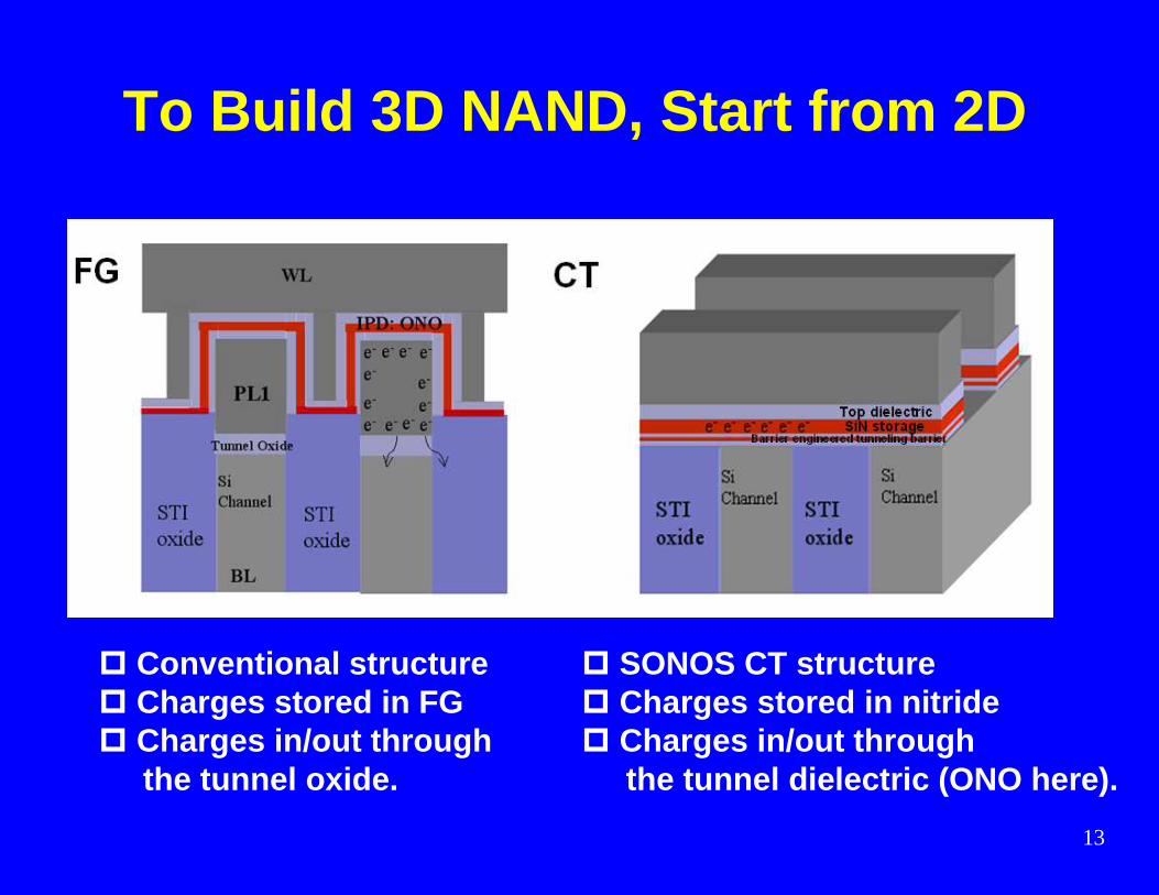
To Build 3D NAND, Start from 2D
� Conventional structure� Charges stored in FG� Charges in/out through
the tunnel oxide.
� SONOS CT structure� Charges stored in nitride� Charges in/out through
the tunnel dielectric (ONO here).
14
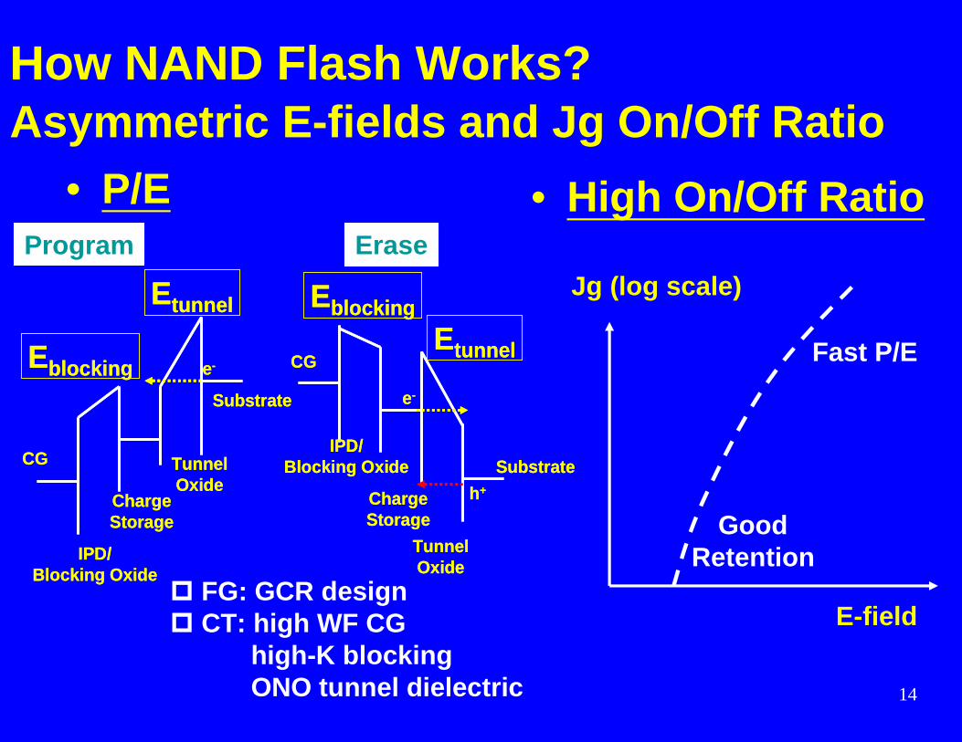
How NAND Flash Works? Asymmetric E-fields and Jg On/Off Ratio
• P/E • High On/Off Ratio
CG
IPD/Blocking Oxide
ChargeStorage
TunnelOxide
Etunnel
EblockingSubstrate
e-
CG
IPD/Blocking Oxide
ChargeStorage
TunnelOxide
Etunnel
EblockingSubstrate
e- CG
IPD/Blocking Oxide
ChargeStorage
TunnelOxide
Etunnel
Eblocking
Substrate
e-
h+
CG
IPD/Blocking Oxide
ChargeStorage
TunnelOxide
Etunnel
Eblocking
Substrate
e-
h+
Program Erase
E-field
Jg (log scale)
Fast P/E
GoodRetention
� FG: GCR design� CT: high WF CG
high-K blockingONO tunnel dielectric
15
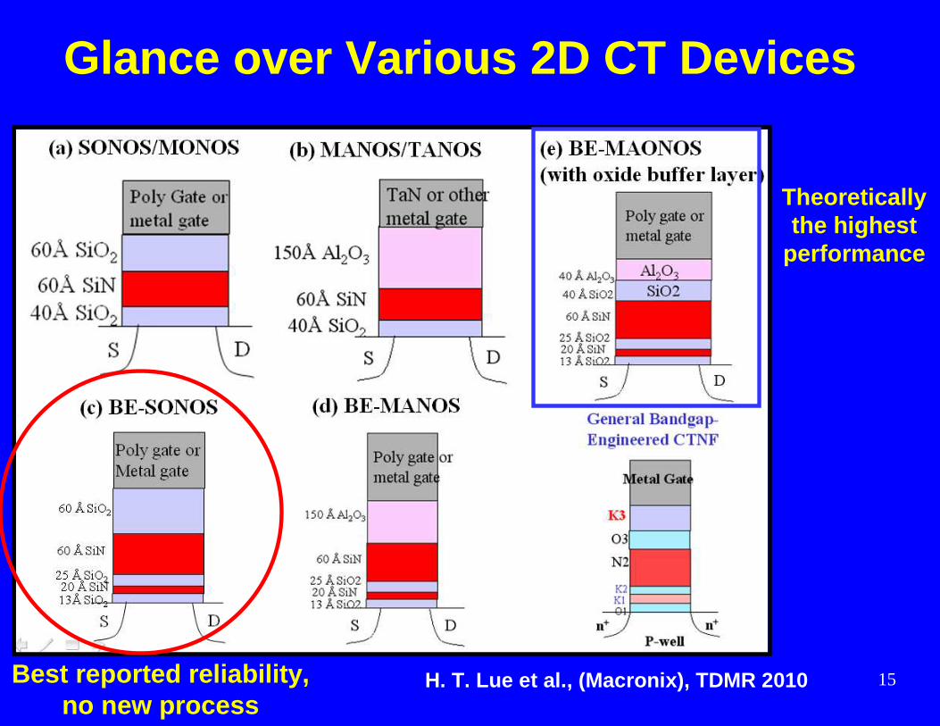
Glance over Various 2D CT Devices
Best reported reliability, no new process
Theoretically the highest
performance
H. T. Lue et al., (Macronix), TDMR 2010
16
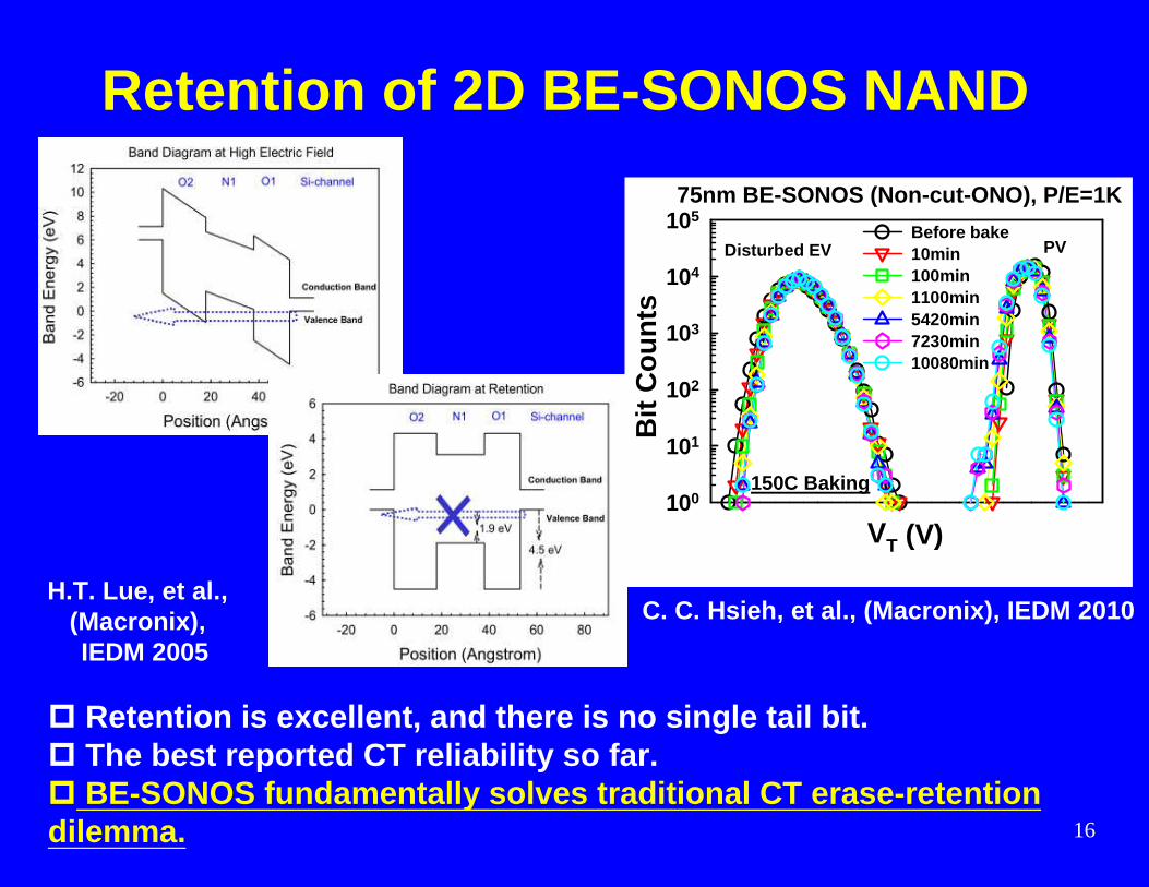
Retention of 2D BE-SONOS NAND
� Retention is excellent, and there is no single tail bit.� The best reported CT reliability so far.� BE-SONOS fundamentally solves traditional CT erase- retention dilemma.
75nm BE-SONOS (Non-cut-ONO), P/E=1K
VT (V)
Bit
Cou
nts
100
101
102
103
104
105Before bake10min100min1100min5420min7230min10080min
PVDisturbed EV
150C Baking
C. C. Hsieh, et al., (Macronix), IEDM 2010H.T. Lue, et al.,
(Macronix), IEDM 2005
17
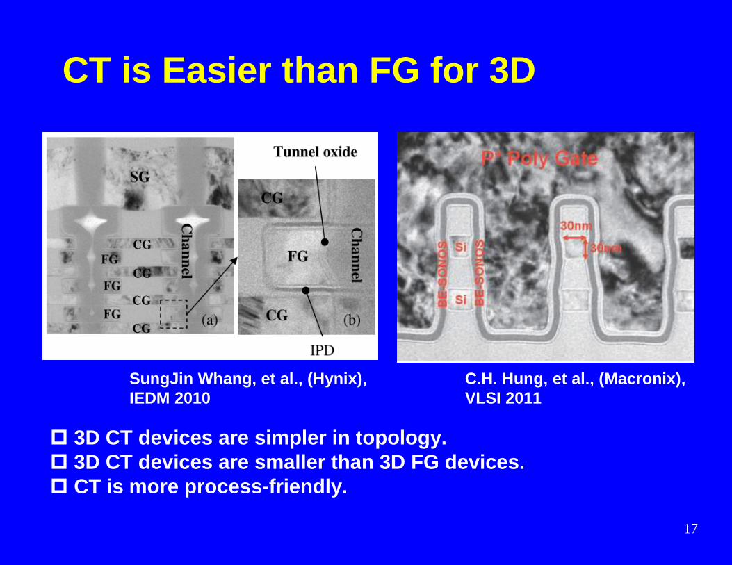
CT is Easier than FG for 3D
� 3D CT devices are simpler in topology.� 3D CT devices are smaller than 3D FG devices.� CT is more process-friendly.
C.H. Hung, et al., (Macronix), VLSI 2011
SungJin Whang, et al., (Hynix), IEDM 2010
18
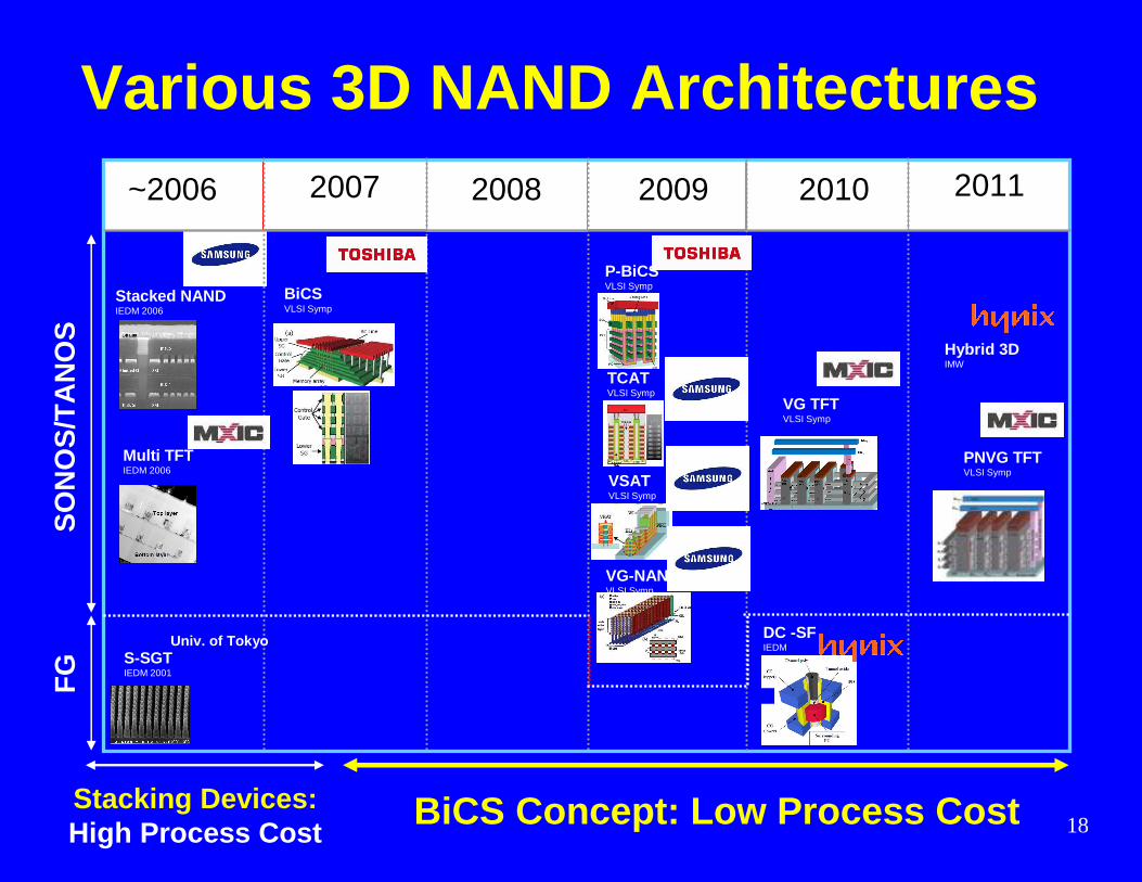
~2006 2007 2008 2009 2010 2011
Stacked NANDIEDM 2006
Multi TFTIEDM 2006
BiCSVLSI Symp
P-BiCSVLSI Symp
VSATVLSI Symp
VG-NANDVLSI Symp
TCATVLSI Symp
VG TFTVLSI Symp
S-SGTIEDM 2001
Univ. of Tokyo DC -SFIEDM
Hybrid 3DIMW
SO
NO
S/T
AN
OS
FG
Stacking Devices:High Process Cost
BiCS Concept: Low Process Cost
Various 3D NAND Architectures
PNVG TFTVLSI Symp
19
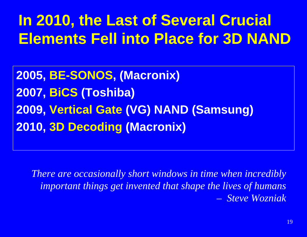
In 2010, the Last of Several Crucial Elements Fell into Place for 3D NAND
2005, BE-SONOS, (Macronix)2007, BiCS (Toshiba)2009, Vertical Gate (VG) NAND (Samsung)2010, 3D Decoding (Macronix)
There are occasionally short windows in time when incredibly important things get invented that shape the lives of humans
– Steve Wozniak
20
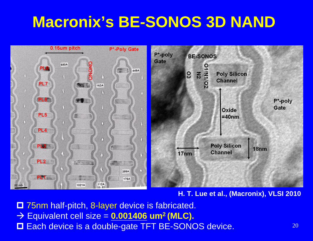
Macronix’s BE-SONOS 3D NAND
� 75nm half-pitch, 8-layer device is fabricated.� Equivalent cell size = 0.001406 um 2 (MLC).� Each device is a double-gate TFT BE-SONOS device.
H. T. Lue et al., (Macronix), VLSI 2010
21
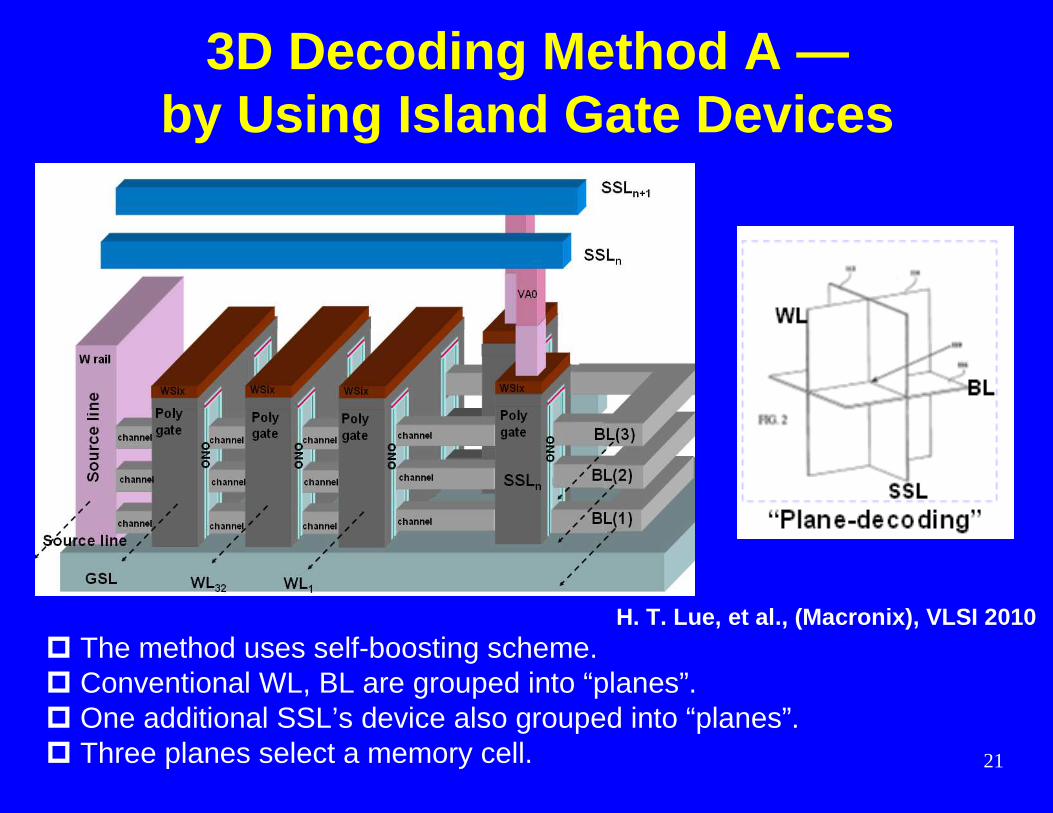
3D Decoding Method A —by Using Island Gate Devices
� The method uses self-boosting scheme.� Conventional WL, BL are grouped into “planes”.� One additional SSL’s device also grouped into “planes”.� Three planes select a memory cell.
H. T. Lue, et al., (Macronix), VLSI 2010
22
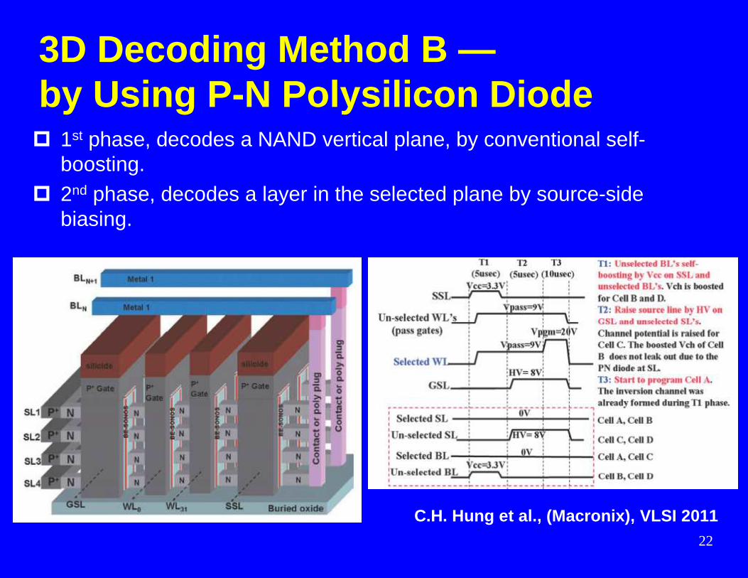
3D Decoding Method B —by Using P-N Polysilicon Diode � 1st phase, decodes a NAND vertical plane, by conventional self-
boosting.� 2nd phase, decodes a layer in the selected plane by source-side
biasing.
C.H. Hung et al., (Macronix), VLSI 2011
23
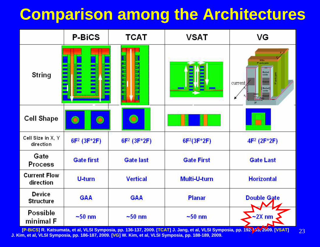
Comparison among the Architectures
[P-BiCS] R. Katsumata, et al, VLSI Symposia, pp. 136-137, 2009. [TCAT] J. Jang, et al, VLSI Symposia, pp. 192-193, 2009. [VSAT] J. Kim, et al, VLSI Symposia, pp. 186-187, 2009. [ VG] W. Kim, et al, VLSI Symposia, pp. 188-189, 2009.
24
Outline
� Why Does NAND Go to 3D?
� Design a 3D NAND Flash Memory
� Challenges and Opportunities in 3D CT NAND Flash Memory
� Summary
25
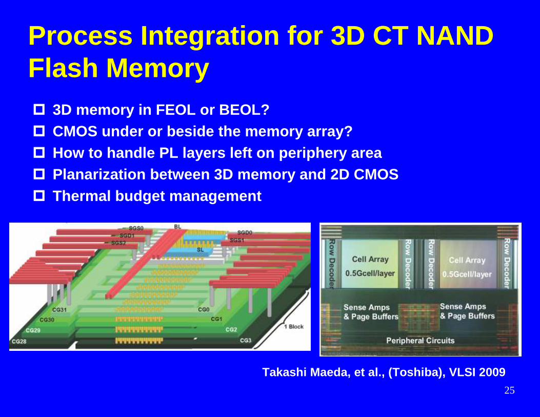
Process Integration for 3D CT NAND Flash Memory� 3D memory in FEOL or BEOL?� CMOS under or beside the memory array?� How to handle PL layers left on periphery area� Planarization between 3D memory and 2D CMOS� Thermal budget management
Takashi Maeda, et al., (Toshiba), VLSI 2009
26
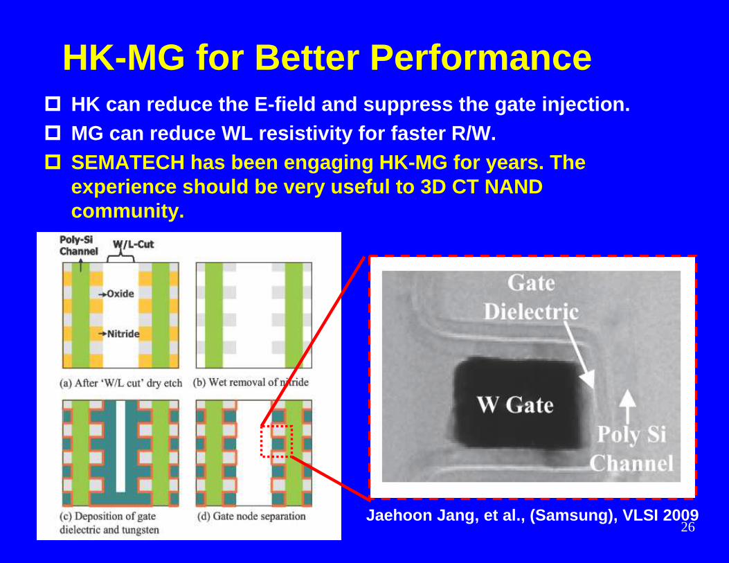
HK-MG for Better Performance� HK can reduce the E-field and suppress the gate inj ection.� MG can reduce WL resistivity for faster R/W. � SEMATECH has been engaging HK-MG for years. The
experience should be very useful to 3D CT NAND community.
Jaehoon Jang, et al., (Samsung), VLSI 2009
27
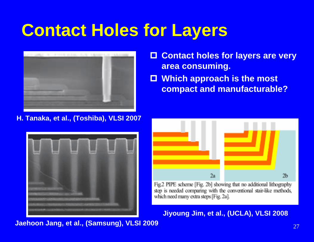
Contact Holes for Layers� Contact holes for layers are very
area consuming. � Which approach is the most
compact and manufacturable?
Jaehoon Jang, et al., (Samsung), VLSI 2009
H. Tanaka, et al., (Toshiba), VLSI 2007
Jiyoung Jim, et al., (UCLA), VLSI 2008
28
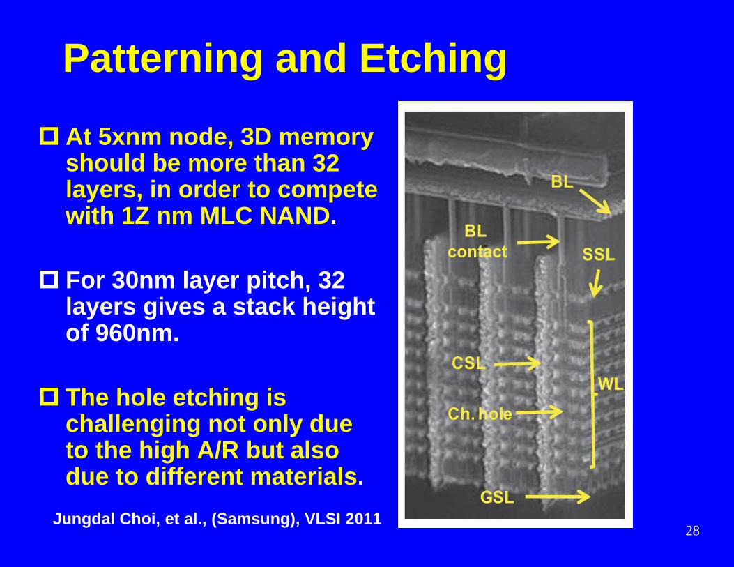
Patterning and Etching
� At 5xnm node, 3D memory should be more than 32 layers, in order to compete with 1Z nm MLC NAND .
� For 30nm layer pitch, 32 layers gives a stack height of 960nm.
� The hole etching is challenging not only due to the high A/R but also due to different materials .
Jungdal Choi, et al., (Samsung), VLSI 2011
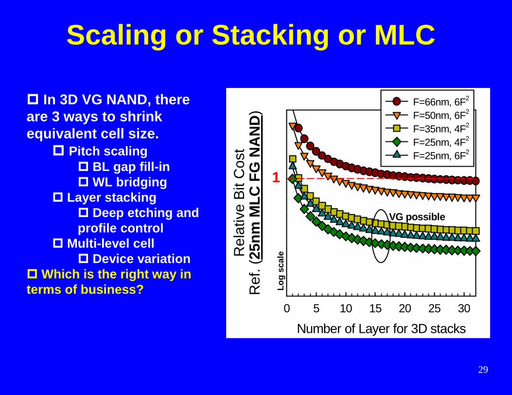
29
Scaling or Stacking or MLC
Number of Layer for 3D stacks
0 5 10 15 20 25 30
Rel
ativ
e B
it C
ost
Ref
. (25
nm M
LC F
G N
AN
D)
F=66nm, 6F2
F=50nm, 6F2
F=35nm, 4F2
F=25nm, 4F2
F=25nm, 6F2
VG possible
1
Log
scal
e
� In 3D VG NAND, there are 3 ways to shrink equivalent cell size.
� Pitch scaling� BL gap fill-in� WL bridging
� Layer stacking� Deep etching and profile control
� Multi-level cell� Device variation
� Which is the right way in terms of business?
30
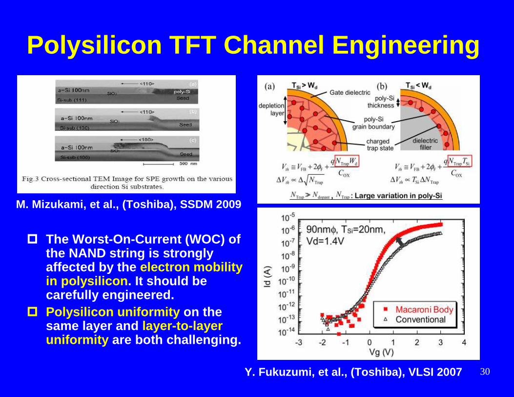
Polysilicon TFT Channel Engineering
� The Worst-On-Current (WOC) of the NAND string is strongly affected by the electron mobility in polysilicon . It should be carefully engineered.
� Polysilicon uniformity on the same layer and layer-to-layer uniformity are both challenging.
Y. Fukuzumi, et al., (Toshiba), VLSI 2007
M. Mizukami, et al., (Toshiba), SSDM 2009
31
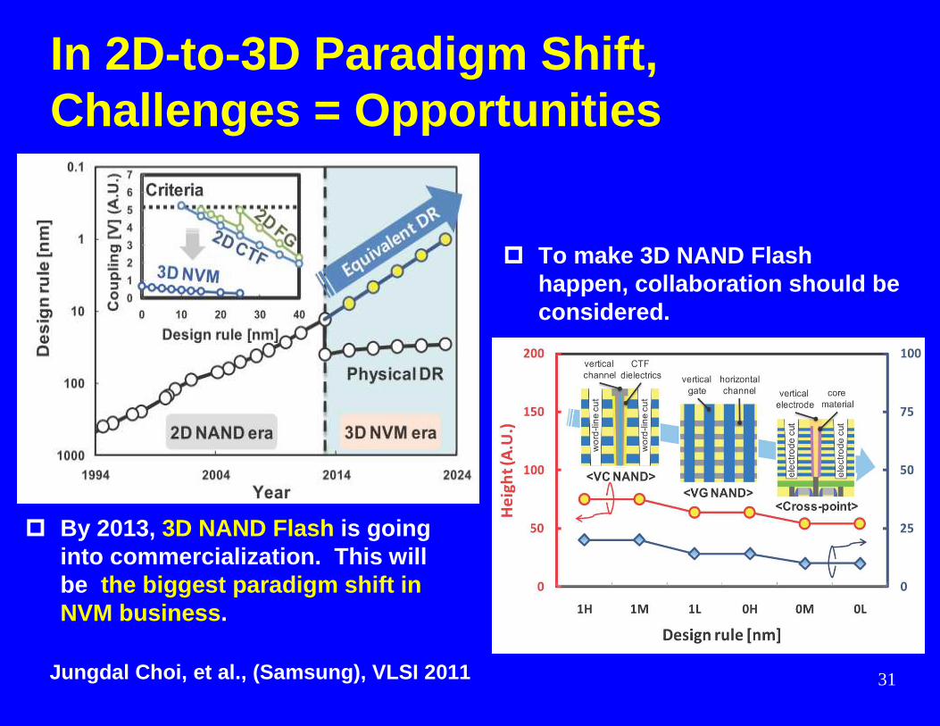
In 2D-to-3D Paradigm Shift, Challenges = Opportunities
� By 2013, 3D NAND Flash is going into commercialization. This will be the biggest paradigm shift in NVM business .
� To make 3D NAND Flashhappen, collaboration should be considered.
Jungdal Choi, et al., (Samsung), VLSI 2011
32
Summary� 2D FG NAND is running out of electrons. 3D is a must to meet demands.
� For 3D NAND Flash, CT type is more process-friendly, and VG is the most scalable architecture.
� Single deep etching (for realizing the BiCSconcept) and polysilicon TFT device uniformity are the most challenging topics.
� Macronix and other NAND giants are dedicated in this field for years. To accelerate the progress, collaboration is a good way, and should be considered.