3d-integrated circuits
DESCRIPTION
The concept of 3-D integration is not new. Although first introduced in 1960, 3-D integration did not materialize until recently because of two reasons: (1) 2-D ICs were already producing results keeping pace with Moore’s law, and (2) technology to remove the tremendous amount of heat from an IC was not available. A combination of technical innovations to produce ultra-low power devices and of future scaling challenges has turned the focus back to 3-D ICs.TRANSCRIPT
3D-INTEGRATED CIRCUITS
3D-INTEGRATED CIRCUITS
Department Of Electronics Page 1

3D-INTEGRATED CIRCUITS
CHAPTER 1
INTRODUCTION
Moore’s law has inspired the growth of integrated circuit (IC) technology since its
inception in 1965. Each new technology node produces smaller and faster devices
keeping pace with Moore’s prediction of 2× scaling every 18 months. The exponential
decrease in feature size, from 10 μm to 22 n over the past four decades, has resulted in an
astronomical performance increase. For this trend to continue, significant challenges need
to be overcome in several key areas. IC technology has evolved from a device-centric
technology to one where interconnect also plays a critical role. The latency of
interconnect dominates that of transistors. Oxide thickness of a metal oxide
semiconductor field effect transistor (MOSFET) determines the size and the leakage
current of a transistor. Oxide thickness approaching atomic levels imposes a practical
bound on the leakage current and hence limits transistor sizes. Exponential increase in
capital cost, to set up a foundry, poses a threat to the viability of future technology
scaling.
Vertical stacking of dies, forming a 3-D IC, is a promising alternative to
traditional 2-D ICs to keep pace with Moore’s Law. 3-D IC technology is not only
capable of increased device-density but also offers heterogeneous integration of dies from
disparate technologies (analog, digital, mixed signals, sensors, antenna, and power
storage) and from different technology nodes (65, 32, 22 nm etc.). The 2009 International
Technology Roadmap for Semiconductor (ITRS) predicts that by 2015 the number of
stacked dies in memory, low-end low-cost, and high-performance chips will be 9, 3, and
2, respectively.
The development of IC technology is driven by the need to increase both
performance and functionality while reducing power and cost. This goal has been
achieved by the use of two solutions: 1) scaling devices and associated interconnecting
wire through the implementation of new materials and processing innovations, and 2)
introducing architecture enhancements to reconfigure routing, hierarchy, and placement
of critical circuit building blocks.
Three-dimensional (3D) integrated circuits (ICs), which contain multiple layers of
active devices, have the potential to dramatically enhance chip performance,
Department Of Electronics Page 2
3D-INTEGRATED CIRCUITS
functionality, and device packing density. They also provide for microchip architecture
and may facilitate the integration of heterogeneous materials, devices, and signals.
However, before these advantages can be realized, key technology challenges of 3D ICs
must be addressed. More specifically, the processes required to build circuits with
multiple layers of active devices must be compatible with current state-of-the-art silicon
processing technology. These processes must also show manufacturability, i.e., reliability,
good yield, maturity, and reasonable cost. To meet these requirements, IBM has
introduced a scheme for building 3D ICs based on the layer transfer of functional circuits,
and many process and design innovations have been implemented. This paper reviews the
process steps and design aspects that were developed at IBM to enable the formation of
stacked device layers. Details regarding an optimized layer transfer process are presented,
including the descriptions of 1) a glass substrate process to enable through-wafer
alignment; 2) oxide fusion bonding and wafer bow compensation methods for improved
alignment tolerance during bonding; 3) and a single-damascene patterning and
metallization method for the creation of high-aspect-ratio (6:1 , AR , 11:1) contacts
between two stacked device layers. This process provides the shortest distance between
the stacked layers (2 lm), the highest interconnection density (108 vias/cm2), and
extremely aggressive wafer-to-wafer alignment (submicron) capability.
1.1 More than Moore with 3-D IC Technology
The concept of 3-D integration is not new. Although first introduced in 1960, 3-D
integration did not materialize until recently because of two reasons: (1) 2-D ICs were
already producing results keeping pace with Moore’s law, and (2) technology to remove
the tremendous amount of heat from an IC was not available. A combination of technical
innovations to produce ultra-low power devices and of future scaling challenges has
turned the focus back to 3-D ICs.
3-D stacking provides exciting design opportunities not possible with 2-D ICs.
Various levels of granularity exist to partition a system to form a 3-D system. Fabricating
individual dies using various technologies and stacking them to form a 3-D IC is an
example of coarse granularity. Monolithic 3-D integration, stacking two dies such that
one die contains all the NMOS transistors and the other contains all the PMOS transistors,
is an example of the finest granularity. Loh et al. provide a detailed architectural analysis
of these granularities. The benefits are many. At the circuit-level, the length of global
wires can be reduced by as much as 50%, wire-limited clock frequency can be increased
Department Of Electronics Page 3
3D-INTEGRATED CIRCUITS
by 3.9×, and wire-limited area can be decreased by 84%. Power requirements can be
reduced by 51% at the 45-nm technology node. At the architecture-level, optimal 3-D
design can be achieved by co-optimizing the architecture and technology at each design
stage.
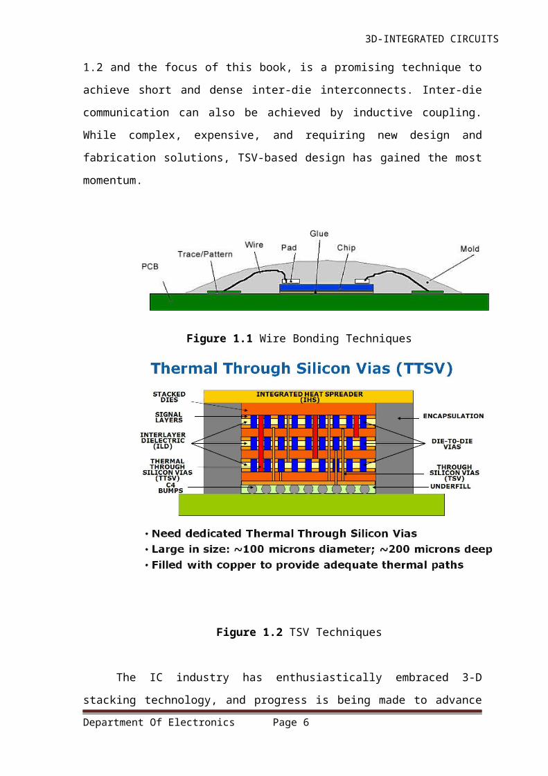
Techniques to achieve 3-D stacking include wire-bonding, monolithic integration,
and through-silicon vias. While straight-forward and economical, wire-bonding is limited
to low-power low-frequency ICs that require less inter-die connections. Wire-bonding
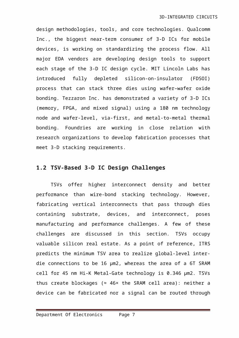
may occur for staggered dies, shown in Fig. 1.1. A monolithic 3-D IC, shown in Fig. 1.1,
requires a new semiconductor manufacturing technique where multiple layers of devices
can be fabricated in a single substrate. This technique offers the most stacking at the
highest cost. TSV-based 3-D integration, shown in Fig. 1.2 and the focus of this book, is a
promising technique to achieve short and dense inter-die interconnects. Inter-die
communication can also be achieved by inductive coupling. While complex, expensive,
and requiring new design and fabrication solutions, TSV-based design has gained the
most momentum.
Figure 1.1 Wire Bonding Techniques
Department Of Electronics Page 4
3D-INTEGRATED CIRCUITS
Figure 1.2 TSV Techniques
The IC industry has enthusiastically embraced 3-D stacking technology, and
progress is being made to advance design methodologies, tools, and core technologies.
Qualcomm Inc., the biggest near-term consumer of 3-D ICs for mobile devices, is
working on standardizing the process flow. All major EDA vendors are developing
design tools to support each stage of the 3-D IC design cycle. MIT Lincoln Labs has
introduced fully depleted silicon-on-insulator (FDSOI) process that can stack three dies
using wafer–wafer oxide bonding. Tezzaron Inc. has demonstrated a variety of 3-D ICs
(memory, FPGA, and mixed signal) using a 180 nm technology node and wafer-level,
via-first, and metal-to-metal thermal bonding. Foundries are working in close relation
with research organizations to develop fabrication processes that meet 3-D stacking
requirements.
1.2 TSV-Based 3-D IC Design Challenges
TSVs offer higher interconnect density and better performance than wire-bond
stacking technology. However, fabricating vertical interconnects that pass through dies
containing substrate, devices, and interconnect, poses manufacturing and performance
challenges. A few of these challenges are discussed in this section. TSVs occupy valuable
silicon real estate. As a point of reference, ITRS predicts the minimum TSV area to
realize global-level inter-die connections to be 16 μm2, whereas the area of a 6T SRAM
cell for 45 nm Hi-K Metal-Gate technology is 0.346 μm2. TSVs thus create blockages (≈
46× the SRAM cell area): neither a device can be fabricated nor a signal can be routed
through the area occupied by a TSV. TSVs therefore impact device density, die floor-
plan, and interconnect routing.
Manufacturing constraints associated with TSV etch and via filling processes
dictate TSV size. Smaller TSV sizes are desirable but require the silicon (Si) substrate to
be thinned to a thickness of 100 to 10 μm, or even less in bulk CMOS technology. To
fabricate a TSV of size 5 μm assuming a practical aspect ratio of 10:1, the maximum die
thickness will be 50 μm. Technical innovations are needed to manufacture and bond thin
wafers.
A TSV is a metallic, usually copper (Cu), interconnect extending through the
substrate and insulated by a dielectric material. Any signal transitions through a TSV
Department Of Electronics Page 5
3D-INTEGRATED CIRCUITS
create noise within abutting substrate. This TSV-induced substrate noise poses a major
threat to the performance of neighboring devices and neighboring TSVs. TSV-induced
substrate noise increases leakage current, which increases static power consumption and
can turn transistors in the “off” state to the “on” state and vice versa.
The large mismatch between the coefficients of thermal expansion (CTE) of
metallic TSV (17.5 E−6/◦C for Cu) and Si substrate (2.5 E−6/◦C) results in serious
reliability concerns. High temperature loadings during fabrication create thermal stress in
the substrate, which in turn impacts the mobility of carriers and affects device
performance. Power delivery design for 3-D ICs is a challenging task due to increased
device density and package asymmetry. While the die closest to the package can get
power supply directly from the package, TSVs are required to deliver power to the dies
further away from the package. TSV size and placement are design decisions. Technology
and design choices must be explored to minimize TSV area penalty and meet power
requirements. Thermal management is one of the biggest problems faced by 3-D IC
design. TSVs can be used to extract heat from the dies away from the heat sink.
Optimizing the number and placement of TSVs to meet the thermal budget requires
accurate modeling and novel algorithmic and design approaches.
1.3Organisation of the report
This report is engaged with an overview of different types of 3D-IC and their
techniques in creating different 3D-IC.This report deals with various advantages and
techniques of 3D-IC over normal IC. This report is organized as follows:
Chapter 1: Introduction-Gives the overview of 3D-IC and different techniques of used in
3D-IC.
Chapter 2: Background- This chapter deals with the main background and types of IC.
Chapter 3: Analysis and Mitigation of TSV-Induced Substrate Noise-This chapter gives
the information about TSV and its substrates.
Chapter 4: TSVs for Power Delivery -This chapter gives the advantages and power
delivery of TSV.
Chapter 5: Early Estimation of TSV Area for Power Delivery in 3-D ICs-This chapter
gives the overview and estimation of TSV power delivery.
Chapter 6: Conclusion-This gives the overview of the whole report with a final
conclusion
Department Of Electronics Page 6
3D-INTEGRATED CIRCUITS
CHAPTER 2
BACKGROUND
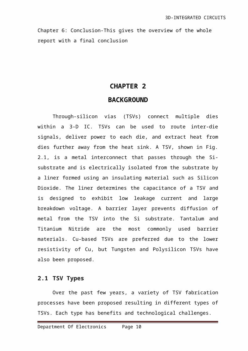
Through-silicon vias (TSVs) connect multiple dies within a 3-D IC. TSVs can be
used to route inter-die signals, deliver power to each die, and extract heat from dies
further away from the heat sink. A TSV, shown in Fig. 2.1, is a metal interconnect that
passes through the Si-substrate and is electrically isolated from the substrate by a liner
formed using an insulating material such as Silicon Dioxide. The liner determines the
capacitance of a TSV and is designed to exhibit low leakage current and large breakdown
voltage. A barrier layer prevents diffusion of metal from the TSV into the Si substrate.
Tantalum and Titanium Nitride are the most commonly used barrier materials. Cu-based
TSVs are preferred due to the lower resistivity of Cu, but Tungsten and Polysilicon TSVs
have also been proposed.
2.1 TSV Types
Over the past few years, a variety of TSV fabrication processes have been
proposed resulting in different types of TSVs. Each type has benefits and technological
challenges.
2.1.1 Regular (Square or Cylindrical) TSV
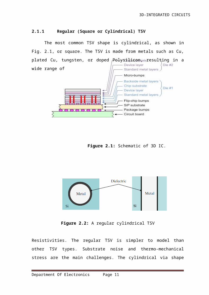
The most common TSV shape is cylindrical, as shown in Fig. 2.1, or square. The
TSV is made from metals such as Cu, plated Cu, tungsten, or doped Polysilicon, resulting
in a wide range of
Department Of Electronics Page 7
3D-INTEGRATED CIRCUITS
Figure 2.1: Schematic of 3D IC.
Figure 2.2: A regular cylindrical TSV
Resistivities. The regular TSV is simpler to model than other TSV types. Substrate noise
and thermo-mechanical stress are the main challenges. The cylindrical via shape allows
for a more uniform insulation layer, and hence a higher breakdown voltage, than for the
square-shaped via.
2.1.2 Annular TSV
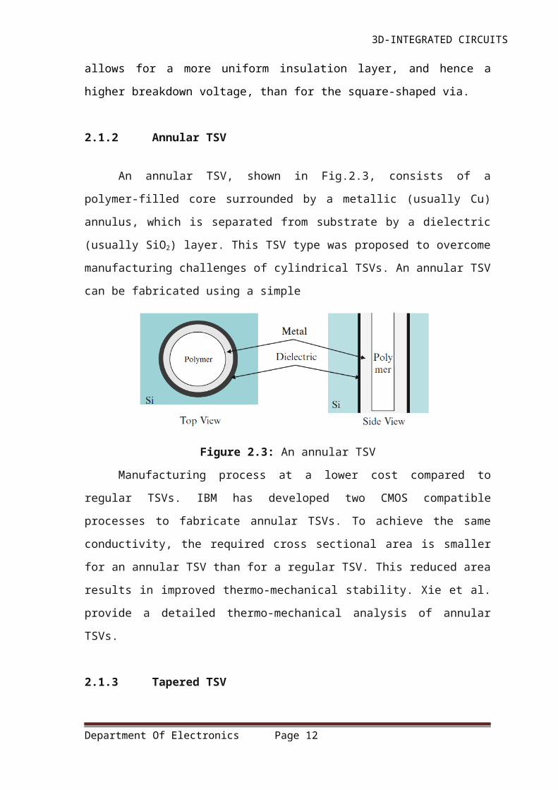
An annular TSV, shown in Fig.2.3, consists of a polymer-filled core surrounded
by a metallic (usually Cu) annulus, which is separated from substrate by a dielectric
(usually SiO2) layer. This TSV type was proposed to overcome manufacturing challenges
of cylindrical TSVs. An annular TSV can be fabricated using a simple
Figure 2.3: An annular TSV
Manufacturing process at a lower cost compared to regular TSVs. IBM has
developed two CMOS compatible processes to fabricate annular TSVs. To achieve the
same conductivity, the required cross sectional area is smaller for an annular TSV than
for a regular TSV. This reduced area results in improved thermo-mechanical stability. Xie
et al. provide a detailed thermo-mechanical analysis of annular TSVs.
Department Of Electronics Page 8
3D-INTEGRATED CIRCUITS
2.1.3 Tapered TSV
The tapered TSV, shown in Fig.2.4, was introduced by MIT Lincoln Laboratory
and has been built in SOI technology. Tapered TSVs in SOI technology do not require
insulation and have lower capacitance than regular TSVs. Tapered TSVs are preferred
over regular TSVs because of their simple fabrication process but tapering results in a
more resistive TSV when compared to a non-tapered one with the same maximal cross-
sectional area. Excessive tapering can be problematic as it leads to V-shaped vias. A
specific interconnect pitch is required at the bottom side of the TSV.
2.1.4 Coaxial TSV
Thin dielectric liner around a TSV and its large extension through the substrate
can create electrical coupling and critical substrate noise in neighboring active devices
and TSVs. A coaxial TSV, first proposed by Sparks et al. and illustrated in Fig.2.5, is a
regular TSV with an added surrounding metal layer. The inner metal layer can be used for
signal transmission while the outer metal layer, connected to circuit ground, provides
shielding. Although a few processes have been proposed to fabricate coaxial TSVs, no
mature technology currently exists to fabricate them.
2.2 TSV Integration
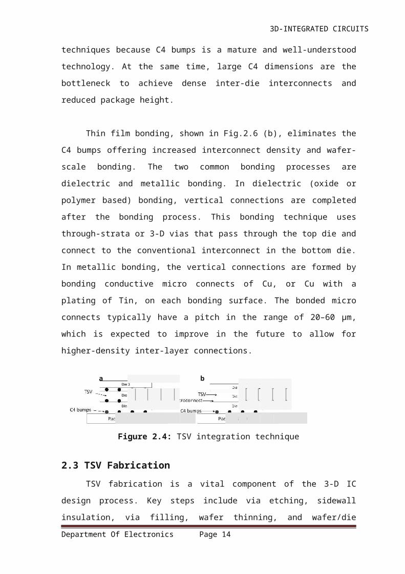
Two common TSV integration techniques are shown in Fig.2.6. Bonding of dies
using controlled collapse chip connect (C4) bumps and TSVs is shown in Fig.2.6 (a). C4-
based TSV integration is the simplest among the two techniques because C4 bumps is a
mature and well-understood technology. At the same time, large C4 dimensions are the
bottleneck to achieve dense inter-die interconnects and reduced package height.
Thin film bonding, shown in Fig.2.6 (b), eliminates the C4 bumps offering
increased interconnect density and wafer-scale bonding. The two common bonding
processes are dielectric and metallic bonding. In dielectric (oxide or polymer based)
bonding, vertical connections are completed after the bonding process. This bonding
technique uses through-strata or 3-D vias that pass through the top die and connect to the
conventional interconnect in the bottom die. In metallic bonding, the vertical connections
are formed by bonding conductive micro connects of Cu, or Cu with a plating of Tin, on
Department Of Electronics Page 9
3D-INTEGRATED CIRCUITS
each bonding surface. The bonded micro connects typically have a pitch in the range of
20–60 μm, which is expected to improve in the future to allow for higher-density inter-
layer connections.
a b
Figure 2.4: TSV integration technique
2.3 TSV Fabrication
TSV fabrication is a vital component of the 3-D IC design process. Key steps
include via etching, sidewall insulation, via filling, wafer thinning, and wafer/die
stacking. Quality and maturity of these process steps determine TSV performance.
Applied has a full line of production-proven systems and processes required for TSV
manufacturing and is leading the efforts, working with consortia and other equipment
suppliers, to enable its adoption.
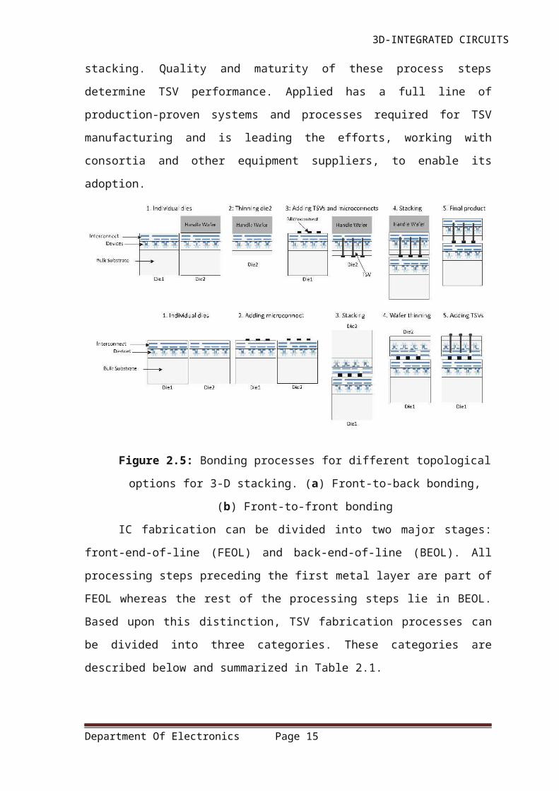
Figure 2.5: Bonding processes for different topological options for 3-D stacking.
(a) Front-to-back bonding, (b) Front-to-front bonding
IC fabrication can be divided into two major stages: front-end-of-line (FEOL) and
back-end-of-line (BEOL). All processing steps preceding the first metal layer are part of
FEOL whereas the rest of the processing steps lie in BEOL. Based upon this distinction,
TSV fabrication processes can be divided into three categories. These categories are
Department Of Electronics Page 10
3D-INTEGRATED CIRCUITS
described below and summarized in Table 2.1.
2.3.1 via First
This is the simplest process where TSVs are fabricated in the bulk substrate before
any devices or interconnect layers are formed. This process does not require any backside
lithography. Moreover, any of the FEOL-compatible processes, including high
temperature thermal oxidation, can be used to deposit TSV insulation. To make this
process FEOL-compatible, the TSV conducting material must be polySi.
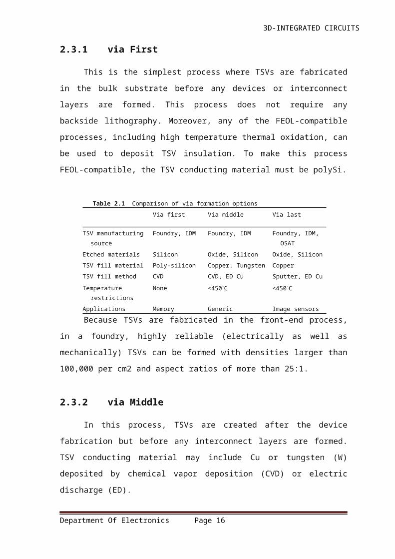
Table 2.1 Comparison of via formation options
Via first Via middle Via last
TSV manufacturing Foundry, IDM Foundry, IDM Foundry, IDM,
source OSAT
Etched materials Silicon Oxide, Silicon Oxide, Silicon
TSV fill material Poly-silicon Copper, Tungsten Copper
TSV fill method CVD CVD, ED Cu Sputter, ED Cu
Temperature None <450◦C <450◦C
restrictions
Applications Memory Generic Image sensors
Because TSVs are fabricated in the front-end process, in a foundry, highly reliable
(electrically as well as mechanically) TSVs can be formed with densities larger than
100,000 per cm2 and aspect ratios of more than 25:1.
2.3.2 via Middle
In this process, TSVs are created after the device fabrication but before any
interconnect layers are formed. TSV conducting material may include Cu or tungsten (W)
deposited by chemical vapor deposition (CVD) or electric discharge (ED).
2.3.3 via Last
In the via last process, TSVs can be fabricated anytime during and after BEOL. Typically,
backside lithography is used to fabricate these vias. For this purpose, a handle-wafer is
attached to the front side of the wafer to be processed. The wafer is thinned and vias are
formed from the backside of substrate. This process is also shown in figure. These TSVs
Department Of Electronics Page 11
3D-INTEGRATED CIRCUITS
need to be connected to lower metal layers (M1 or M2) of the die to avoid etching
through the higher metal layers. This process requires a low-temperature TSV insulation
technique to minimize thermal effects on already fabricated devices and interconnect.
Other challenges include backside lithography, wafer-thinning and handling, and reliably
opening the insulation at the base of the vias to make reliable electrical connections.
2.4 Electrical Modeling of TSVs
Using resistive, inductive, and capacitive elements, a TSV can be modeled as a
circuit component. TSV performance (signal delay and power dissipation) is governed by
the values of these RLC elements. Various approaches have been considered to extract
relevant RLC parameters. We describe an overview of these approaches.
The simplest approach is to estimate the R and C values of a TSV using basic
calculations:
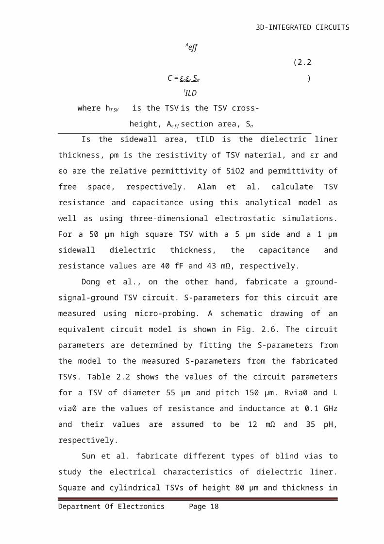
R = ρ m h T SV (2.1)Aeff
C = εoεr Sa (2.2)tILD
where hT SV is the TSV height, Ae f f is the TSV cross-section area, Sa
Is the sidewall area, tILD is the dielectric liner thickness, ρm is the resistivity of
TSV material, and εr and εo are the relative permittivity of SiO2 and permittivity of free
space, respectively. Alam et al. calculate TSV resistance and capacitance using this
analytical model as well as using three-dimensional electrostatic simulations. For a 50 μm
high square TSV with a 5 μm side and a 1 μm sidewall dielectric thickness, the
capacitance and resistance values are 40 fF and 43 mΩ, respectively.
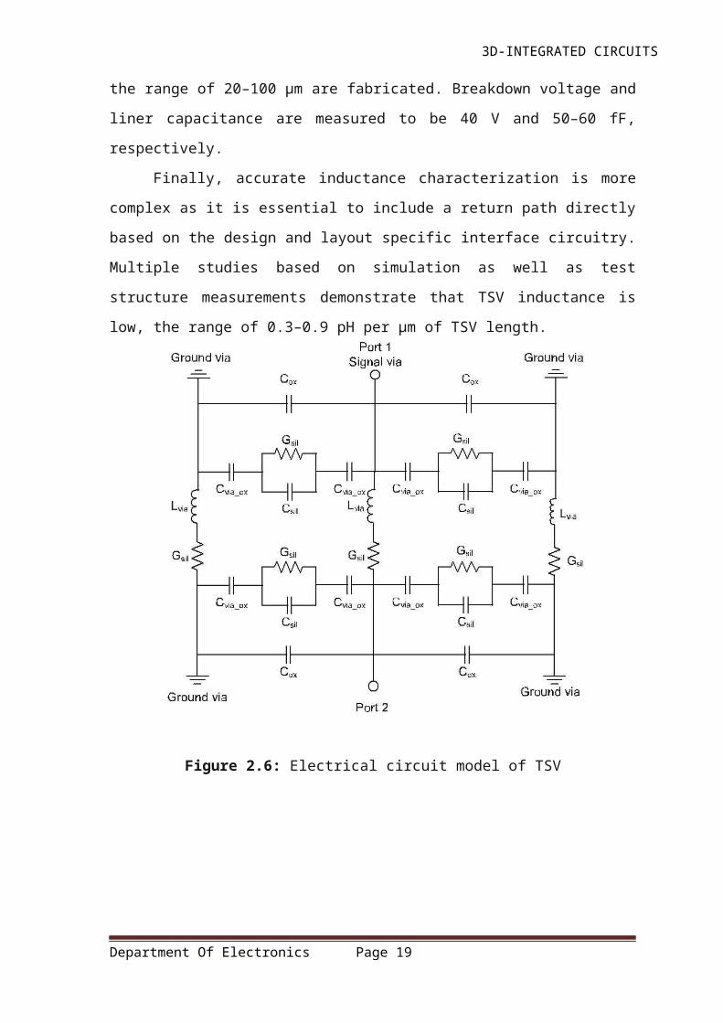
Dong et al., on the other hand, fabricate a ground-signal-ground TSV circuit. S-
parameters for this circuit are measured using micro-probing. A schematic drawing of an
equivalent circuit model is shown in Fig. 2.6. The circuit parameters are determined by
fitting the S-parameters from the model to the measured S-parameters from the fabricated
TSVs. Table 2.2 shows the values of the circuit parameters for a TSV of diameter 55 μm
and pitch 150 μm. Rvia0 and L via0 are the values of resistance and inductance at 0.1
GHz and their values are assumed to be 12 mΩ and 35 pH, respectively.
Sun et al. fabricate different types of blind vias to study the electrical
characteristics of dielectric liner. Square and cylindrical TSVs of height 80 μm and
thickness in the range of 20–100 μm are fabricated. Breakdown voltage and liner
Department Of Electronics Page 12
3D-INTEGRATED CIRCUITS
capacitance are measured to be 40 V and 50–60 fF, respectively.
Finally, accurate inductance characterization is more complex as it is essential to
include a return path directly based on the design and layout specific interface circuitry.
Multiple studies based on simulation as well as test structure measurements demonstrate
that TSV inductance is low, the range of 0.3–0.9 pH per μm of TSV length.
Figure 2.6: Electrical circuit model of TSV
Department Of Electronics Page 13
Table 2.2 Circuit parameters for TSV of diameter 55 μm
Parameter Description Value
Rvia TSV resistance Rvia0 1 +f
108
Lvia TSV inductance
Lvia0
1+log(
f )0.2
68
Cvia−ox
10
Capacitance of TSV liner 910 fFCox Capacitance of the oxide layer on 3 fF
the silicon surface and the
fringing field between the viasCsil Capacitance of the silicon substrate 9 fF
Gsil loss property of the silicon 1.69 m/Ω
3D-INTEGRATED CIRCUITS
CHAPTER 3
ANALYSIS AND MITIGATION OF TSV-INDUCED
SUBSTRATE NOISE
TSVs are a major source of substrate noise that threatens the performance of
neighboring devices. In addition, TSV noise increases leakage current, which increases
static power consumption and can erroneously switch transistors off or on. A “keep out”
zone, specified through layout rules, is thus required to shield devices from neighboring
TSVs.
We study in this chapter the TSV-induced substrate noise problem and analyze the
effectiveness of different noise mitigation techniques. We propose a practical and
effective device, a ground (GND) plug, to reduce TSV-induced substrate noise. A GND
plug is a TSV-like structure that is connected to circuit ground and may extend partially
or completely through the substrate. Multiple GND plugs, fabricated around a TSV,
provide noise isolation between TSVs and neighboring devices. We examine the physical
design and placement of GND plugs for effective noise isolation. We compare the GND
plug technique with two other noise mitigation techniques: thicker dielectric liner and
backside ground plane. Thicker dielectric liner provides shielding that decreases coupling
between TSV and substrate. A backside plane, electrically connected to circuit GND,
ensures sufficient substrate grounding.
The rest of the chapter is organized as follows. We present an overview of TSV-
induced noise and related work in Sect. 3.1. We describe an evaluation framework used to
perform lumped parasitic analysis in Sect. 3.1. We perform a comparison of three
different noise mitigation techniques: thicker dielectric liner, backside ground, and GND
plugs in Sect. 3.1. We provide the summary in Sect. 3.1.
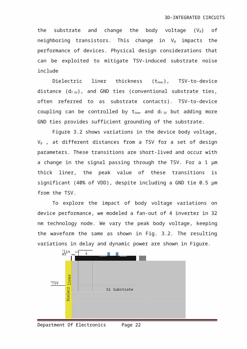
3.1 Problem: TSV-Induced Noise
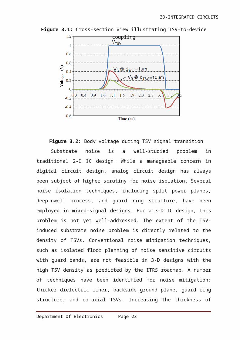
Figure 3.1 shows a cross-section view of a Silicon (Si) substrate with a TSV and a
Department Of Electronics Page 14
3D-INTEGRATED CIRCUITS
MOSFET transistor. Signal transitions through a TSV create noise that can pass through
the substrate and change the body voltage (VB) of neighboring transistors. This change in
VB impacts the performance of devices. Physical design considerations that can be
exploited to mitigate TSV-induced substrate noise include
Dielectric liner thickness (tliner), TSV-to-device distance (dT SV), and GND ties
(conventional substrate ties, often referred to as substrate contacts). TSV-to-device
coupling can be controlled by tliner and dT SV but adding more GND ties provides sufficient
grounding of the substrate.
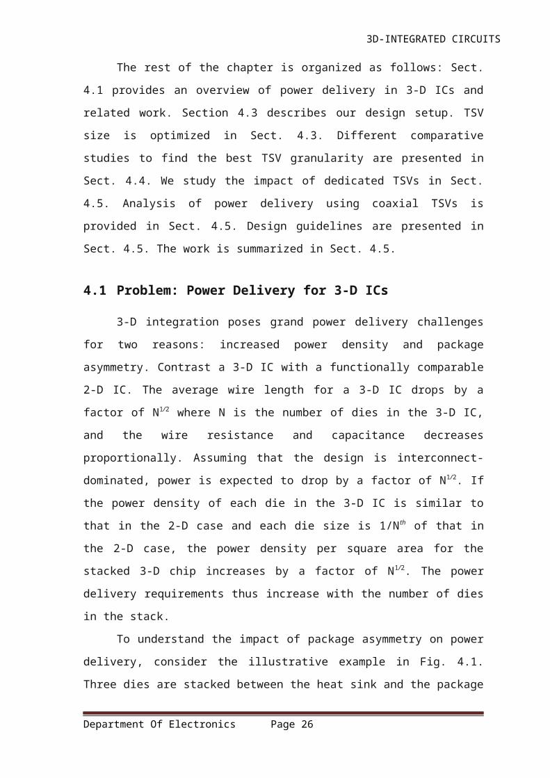
Figure 3.2 shows variations in the device body voltage, VB , at different distances
from a TSV for a set of design parameters. These transitions are short-lived and occur
with a change in the signal passing through the TSV. For a 1 μm thick liner, the peak
value of these transitions is significant (40% of VDD), despite including a GND tie 0.5
μm from the TSV.
To explore the impact of body voltage variations on device performance, we
modeled a fan-out of 4 inverter in 32 nm technology node. We vary the peak body
voltage, keeping the waveform the same as shown in Fig. 3.2. The resulting variations in
delay and dynamic power are shown in Figure.tliner
VTSV liner
Die
lecr
ict
Si Substrate
Figure 3.1: Cross-section view illustrating TSV-to-device coupling
Department Of Electronics Page 15
3D-INTEGRATED CIRCUITS
Figure 3.2: Body voltage during TSV signal transition
Substrate noise is a well-studied problem in traditional 2-D IC design. While a
manageable concern in digital circuit design, analog circuit design has always been
subject of higher scrutiny for noise isolation. Several noise isolation techniques, including
split power planes, deep-nwell process, and guard ring structure, have been employed in
mixed-signal designs. For a 3-D IC design, this problem is not yet well-addressed. The
extent of the TSV-induced substrate noise problem is directly related to the density of
TSVs. Conventional noise mitigation techniques, such as isolated floor planning of noise
sensitive circuits with guard bands, are not feasible in 3-D designs with the high TSV
density as predicted by the ITRS roadmap. A number of techniques have been identified
for noise mitigation: thicker dielectric liner, backside ground plane, guard ring structure,
and co-axial TSVs. Increasing the thickness of the dielectric liner surrounding a TSV is
the simplest approach. Increased liner thickness has already been shown to be insufficient
in mitigating substrate noise. Providing a backside ground by placing a die on a grounded
metal sheet is a common strategy to mitigate substrate noise in 2-D ICs. This strategy
may not be practical for 3-D ICs because of two reasons: (1) a metallic sheet between dies
will introduce unnecessary inductive coupling, (2) design complexity will increase
because TSVs passing through metallic sheets must be isolated. Surrounding TSVs with
guard rings is not effective because typical guard-ring depth is comparable to GND tie
depth, which is too small to provide any significant isolation. Lastly, using a co-axial
TSV is promising to mitigate noise but the manufacturability of co-axial TSVs is still in
question.
Department Of Electronics Page 16
3D-INTEGRATED CIRCUITS
CHAPTER 4
TSV’S FOR POWER DELIVERY
Robust power delivery is one of the ITRS scaling grand challenges due to
increasing operating frequencies, increasing power density, and decreasing supply
voltages. Three dimensional stacking of multiple dies makes this problem even more
challenging. In a 3-D IC, only the die adjacent to the package can get power directly from
the package. Dies away from the package require new technologies for power delivery.
We evaluate in this chapter using TSVs to deliver power in a 3-D IC with the goal of
understanding factors that contribute to the performance of a 3-D power delivery network
(PDN). We investigate the impact of TSV size. We study various architectural
configurations to find the best TSV granularity. We explore the impact of shared and
dedicated TSVs on PDN performance and the feasibility of coaxial TSVs for power
delivery.
We measure PDN performance in terms of maximum, average, and standard
deviations of IR drops and Ldi/dt droop. These metrics quantify local and global PDN
characteristics in both dc and transient analysis. Our evaluation framework consists of a
four-core chip multiprocessor (CMP), a memory (MEM), and an accelerator engine
(ACCL). We use realistic workloads from SPEC benchmarks for each functional module
in the system. The PDN for our 3-D designs is modeled using both off-chip and on-chip
components.
The rest of the chapter is organized as follows: Sect. 4.1 provides an overview of
power delivery in 3-D ICs and related work. Section 4.3 describes our design setup. TSV
size is optimized in Sect. 4.3. Different comparative studies to find the best TSV
granularity are presented in Sect. 4.4. We study the impact of dedicated TSVs in Sect.
4.5. Analysis of power delivery using coaxial TSVs is provided in Sect. 4.5. Design
guidelines are presented in Sect. 4.5. The work is summarized in Sect. 4.5.
4.1 Problem: Power Delivery for 3-D ICs
3-D integration poses grand power delivery challenges for two reasons: increased
power density and package asymmetry. Contrast a 3-D IC with a functionally comparable
Department Of Electronics Page 17
3D-INTEGRATED CIRCUITS
2-D IC. The average wire length for a 3-D IC drops by a factor of N1/2 where N is the
number of dies in the 3-D IC, and the wire resistance and capacitance decreases
proportionally. Assuming that the design is interconnect-dominated, power is expected to
drop by a factor of N1/2. If the power density of each die in the 3-D IC is similar to that in
the 2-D case and each die size is 1/Nth of that in the 2-D case, the power density per
square area for the stacked 3-D chip increases by a factor of N1/2. The power delivery
requirements thus increase with the number of dies in the stack.
To understand the impact of package asymmetry on power delivery, consider the
illustrative example in Fig. 4.1. Three dies are stacked between the heat sink and the
package substrate. Electric signals and power are routed from the printed circuit board to
the package substrate through ceramic ball grid array (CBGA) joints, and then they are
distributed utilizing controlled collapsed chip connections (C4). The dies are bonded
using micro connects. Through-silicon vias (TSVs) pass through a die and provide
electrical connectivity for signals or power delivery among the dies. Clearly, the package
asymmetry impacts both power delivery and heat removal, another critical challenge in 3-
D ICs. While thermal issues have received considerable attention, e.g. 3-D power delivery
has not yet been adequately addressed.
Previous work on 3-D power delivery can be summarized under two main themes:
power delivery techniques and power integrity analysis. Kim et al. analyzed a multistory
power delivery technique where a higher than nominal VDD supply voltage is applied
from the package and distributed differentially to subsequent power rails using level
conversion.
Figure 4.1: Illustrative 3D system assuming face-to-back metallic.
Most of the previous works assume worst case switching currents and utilize
Department Of Electronics Page 18
3D-INTEGRATED CIRCUITS
overly simplified power grid network models. In contrast, our work utilizes a more
detailed off-chip and on-chip PDN in a realistic design example where we use a workload
derived from SPEC benchmarks. We estimate both IR drop and Ldi/dt droop in 3-D PDN.
In addition to quantify the impact of TSV size, TSV spacing, and C4 spacing, we
investigate the impact of coaxial TSVs and their novel usage in 3-D PDN.
4.2 Design Setup
4.2.1 3-D Stacked Architecture
We use a 3-D IC consisting of three dies: a quad-core chip-multiprocessor
(PROC), a memory (MEM), and an accelerator engine (ACCL). Figure 4.2 shows the
cross-section of our 3-D chip. Each die is assumed to have an area of 1 cm2. We consider
the thermal/power profile of each die while considering their placement in the 3-D chip.
Since PROC has the highest power consumption, we place it adjacent to the heat sink. We
place ACCL farthest from the heat sink due to its lowest power consumption. MEM is
placed at the center of the stack to allow shorter access paths from/to both PROC and
ACCL. Each core of the CMP utilizes 10 W of maximum power, and is composed of five
functional blocks: floating point unit (FPU), OOO (the rename, register file, result-bus,
and window units), INT (integer arithmetic logic unit), and Fetch (combines the
instruction cache and branch predictor), and Data (represents the data cache and load-
store queue). The MEM and ACCL modules utilize a maximum of 20 and 10 W,
respectively. The maximum power consumed by the 3-D IC is 70 W. MEM is assumed to
generate a current trace similar to that of the L2 Cache; ACCL is assumed to generate a
current trace similar to that of the FPU block.
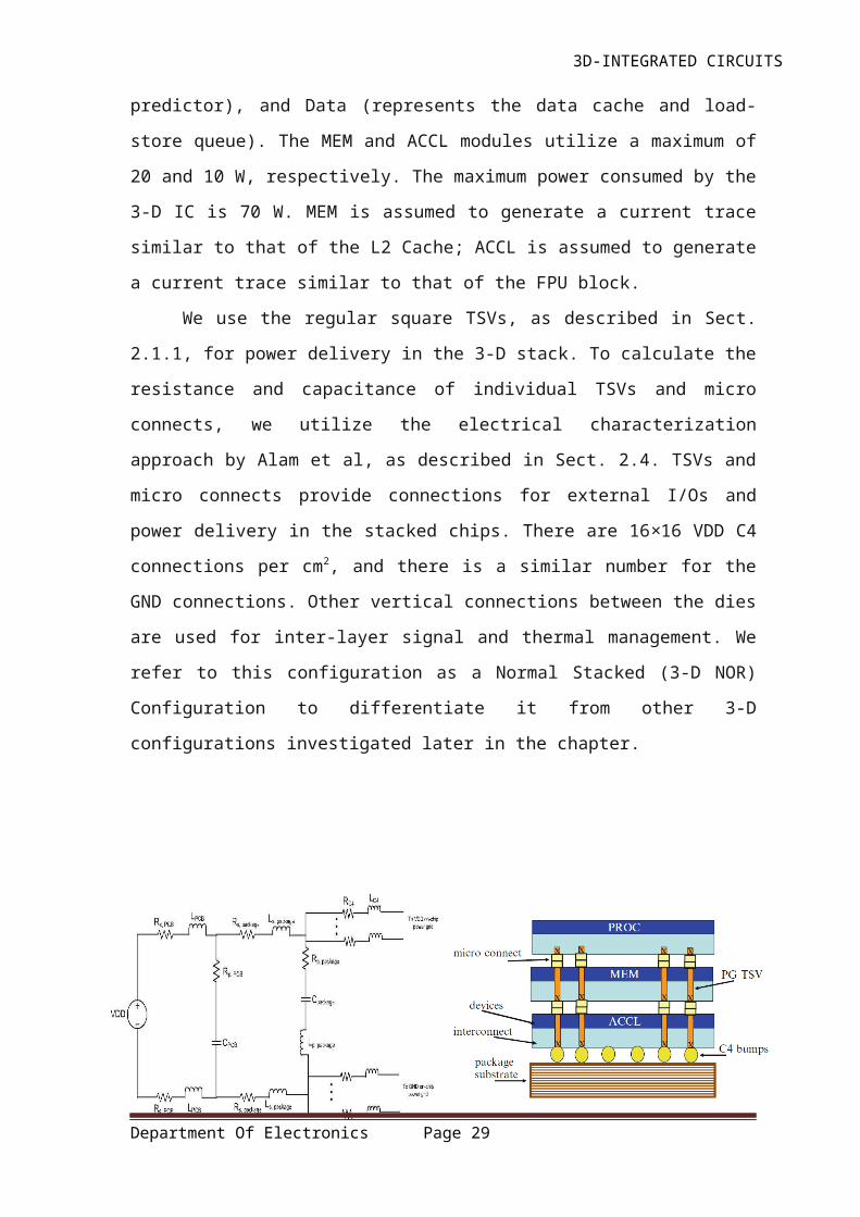
We use the regular square TSVs, as described in Sect. 2.1.1, for power delivery in
the 3-D stack. To calculate the resistance and capacitance of individual TSVs and micro
connects, we utilize the electrical characterization approach by Alam et al, as described in
Sect. 2.4. TSVs and micro connects provide connections for external I/Os and power
delivery in the stacked chips. There are 16×16 VDD C4 connections per cm2, and there is
a similar number for the GND connections. Other vertical connections between the dies
are used for inter-layer signal and thermal management. We refer to this configuration as
a Normal Stacked (3-D NOR) Configuration to differentiate it from other 3-D
configurations investigated later in the chapter.
Department Of Electronics Page 19

3D-INTEGRATED CIRCUITS
Figure 4.3: Off-chip power delivery Figure 4.2: Normal Stacked (3DNOR)
4.2.2 Power Delivery Network (PDN)
The PDN model is illustrated in Figs. 4.3 and 4.4. The off-chip (motherboard and
package), shown in Fig. 4.3, network is modeled as a resistive, inductive and capacitive
network. The on-chip network, shown in Fig. 4.4, consists of a global-level, grid-like
structure routed in top metal layers. We model the load imposed on the global grid as
time varying current sources. The off-chip and on-chip networks are connected using
series resistors and inductors representing the flip-chip package.
For the on-chip power grid, each grid element is modeled as a resistance and an
inductance in series. In addition, current load points and micro connect or TSV points
(TSV-P) alternate throughout the grid as shown in Fig. 4.4. The TSV-Ps is connected to
the C4 bumps either directly or through other stacked layers depending on the position of
the on-chip PDN in the stack. The length of a grid element is such that we have a 16×16
element grid. We assume wide metal line widths such that the grid collectively occupies
50% of the total die area in the top two metal layers. We use the predictive technology
model to calculate the R & L for grid elements. A fast circuit solver, based on
preconditioned Krylov subspace iterative methods, is used to solve the SPICE net list for
the modeled configuration. A decoupling capacitance of 33 nF/cm2 is assumed in our
study, corresponding to device capacitance implementation with 1 nm gate oxide
thickness (from the ITRS roadmap of 90 nm, 65 nm technology) occupying 20% of die
area. The decoupling capacitance is uniformly distributed along the grid elements in our
3-D IC.
4.2.3 Trace Selection
Department Of Electronics Page 20
3D-INTEGRATED CIRCUITS
The power demand of the functional blocks is critical in evaluating the PDN
performance. A simple strategy is to use the SPEC benchmarks to extract per cycle power
demands of each functional block and analyze the PDN at each cycle. This strategy will
give precise results but simulating the PDN for millions of cycles is time consuming.
Another strategy is to extract the worst case power demands for each functional block and
evaluate PDN performance for this worst case. While this strategy tremendously reduces
the simulation time, the results are pessimistic as blocks typically do not operate at peak
power at the same time, nor do they change current demand simultaneously. We use a
trace compression strategy that reduces the simulation time without compromising the
accuracy. The PDN associated with PCB plays a vital role in maintaining system integrity
i.e. necessary fidelity of signal and clock wave shapes, and minimizing electromagnetic
noise generation. As integrated circuit (IC) technology is scaled downward to yield
smaller and faster transistors, the power supply voltage must decrease. As clock rates rise
and more functions are integrated into microprocessors and application specific integrated
circuits (ASICs), the power consumed must increase, meaning that current levels.
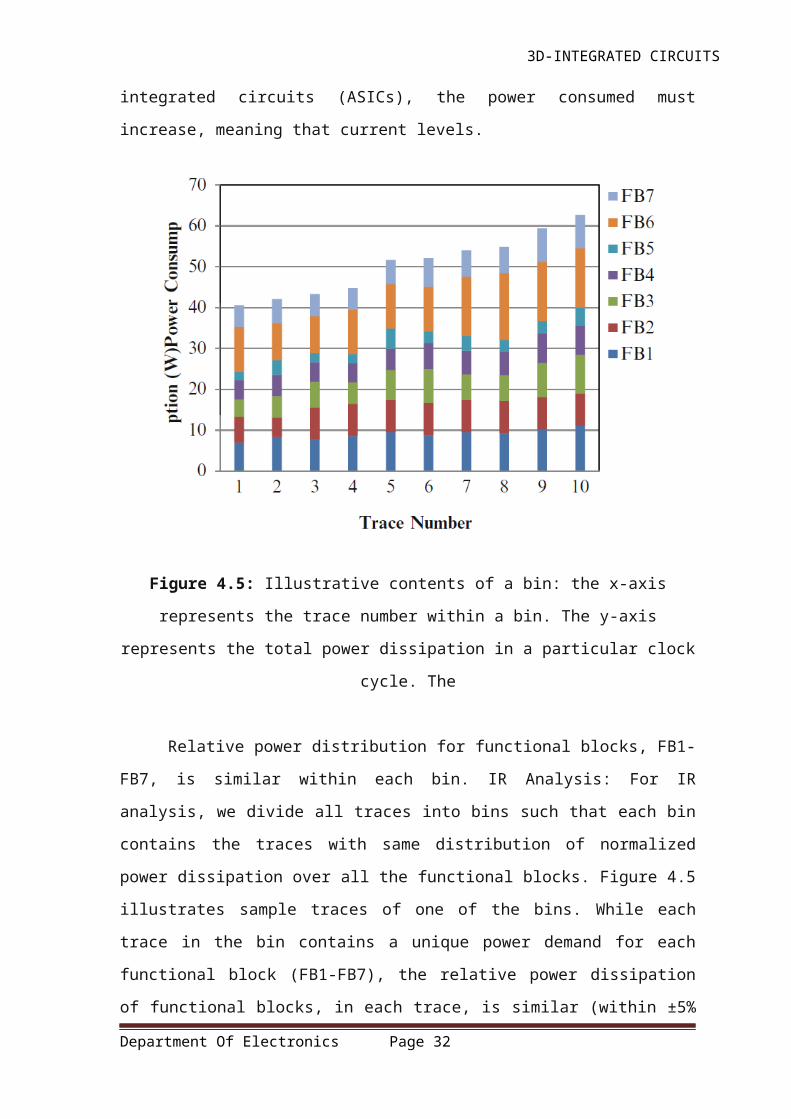
Figure 4.5: Illustrative contents of a bin: the x-axis represents the trace number within a
bin. The y-axis represents the total power dissipation in a particular clock cycle. The
Relative power distribution for functional blocks, FB1-FB7, is similar within each
bin. IR Analysis: For IR analysis, we divide all traces into bins such that each bin
Department Of Electronics Page 21
3D-INTEGRATED CIRCUITS
contains the traces with same distribution of normalized power dissipation over all the
functional blocks. Figure 4.5 illustrates sample traces of one of the bins. While each trace
in the bin contains a unique power demand for each functional block (FB1-FB7), the
relative power dissipation of functional blocks, in each trace, is similar (within ±5%
variations). Relative power consumptions of the functional blocks determine the
capability of the PDN to share power for neighboring functional blocks. For each bin, we
simulate only the trace with the largest total power consumption; for example, trace 10
will be simulated representing the bin shown in Fig. 4.5. We used this approach on 10
million traces of four benchmarks and we were able to reduce the number of traces to
1,428.
Ldi/dt Analysis: For Ldi/dt analysis, we use current traces that represent a variety
of current patterns: step, pulse, and resonating. These patterns were derived based on the
work of Meeta et al, where four SPEC workloads (apsi, bzip, equake, and mcf) were run
for 100 million instructions using Watch , and 2,048 cycle snippets (8,192 total traces)
representing the current patterns were then extracted. Such a power grid evaluation
methodology replaces observing millions of instructions from a wide variety of
benchmarks, thus significantly saving power grid simulation times.
4.3 Optimal TSV Size for 3-D PDN
We examine in this section how TSV size impacts 3-D power delivery. TSV size
is the dimension of one side of the square TSV footprint. The TSV height is always equal
to die thickness, which is 50 μm in all our 3-D setups.
Department Of Electronics Page 22
3D-INTEGRATED CIRCUITS
Figure 4.4: Maximum and average IR drop for various TSV sizes. (a) Maximum IR drop, (b) Average IR drop
The maximum and average IR drops in different dies, for TSV sizes ranging from
5 to 50 μm in the 3-D NOR configuration, are shown in Fig. 4.4. We can make the
following observations: The ACCL, directly connected to C4 bumps, exhibits nearly
constant maximum and average IR drops across the different TSV sizes. As TSV size is
increased, there is a slight increase in both maximum and average IR drop. This
represents the fact that the grid sharing capability is improved with the increased TSV
size. More importantly, the IR drop saturates in PROC and MEM for TSV sizes of and
greater than 20 μm. Such saturation suggests the lack of benefit of increasing the TSV
size beyond a specific size. A TSV size of 25 μm is therefore used in the following
analysis for 3-D PDN.
Department Of Electronics Page 23

3D-INTEGRATED CIRCUITS
CHAPTER 5
EARLY ESTIMATION OF TSV AREA FOR POWER DELIVERY IN 3-D IC’S
To harness the full potential of 3-D integrated circuits, analysis tools for early
design space exploration are needed. Such tools, targeting multiple design facets and cost
trade-off analysis, would allow designers to arrive at major decisions regarding
architecture and implementations fabrics. TSVs neither occupy valuable silicon real estate
and neither device nor interconnects can be formed in the area occupied by a TSV. An
early estimation of total TSV area allows effective budgeting of device and interconnects
resources.
We provide in this chapter a set of algorithms to estimate the minimal substrate
area required for TSV-based power delivery. These algorithms can be applied early in the
design stages when only functional block-level behaviors and a floor plan are available.
Our proposed work is in contrast with recent TSV optimization techniques, which are
applied later in the design cycle to target optimal signal TSV placement. Planning for
signal TSVs clearly requires detailed circuit layout. Our optimization framework can be
extended for investigating using TSVs for heat removal if realistic thermal modeling is
appropriately utilized. Studies supporting the use of TSVs for heat removals are still in
their early stages and do not consider realistic manufacturing constraints.
The rest of the chapter is organized as follows: Related work is presented in Sect.
5.1. The problem of power TSV area minimization is formulated in Sect. 5.2. Our
proposed algorithms are presented in Sect. 5.3. We discuss our results in Sect. 5.4. We
summarize our work in Sect. 5.4.
5.1 Related Work
To optimize TSV area, Lee et al. investigated a co-optimization methodology for
signal, power, and thermal TSVs based on design of experiments and response surface
method, and they showed that careful tuning of response surface models can lead to
reliable optimization results. Current TSV co-optimization techniques thus pro-vide
insights but have neglected key TSV manufacturing constraints. While functional data
Department Of Electronics Page 24

3D-INTEGRATED CIRCUITS
early in the design cycle can be used to estimate thermal profiles, studies addressing the
manufacturing concerns are needed to further explore the benefits of thermal TSVs. Each
TSV must have a liner, an insulating material filled around the TSV, to provide isolation
as well as stop metal diffusion into substrate. This insulating material helps to reduce
TSV-induced substrate noise but deteriorates TSV performance to extract heat from
substrate. A model of thermal TSV without liner is, thus, not accurate and none of the
previous models of thermal TSV include liner. Mechanical stress associated with TSV
calls for a keep-away area where no devices can be fabricated. Therefore TSVs cannot be
directly connected to a hotspot or any floor plan tile as assumed in Power TSVs connects
to only the top metal layers. The efficiency of heat extraction from the surrounding
volume is unclear.
While this chapter investigates power TSV optimization, independently of thermal
TSVs, the iterative framework can be Interconnects can be fabricated. Bart et al. suggest
that the keep-away area increases with the increase in TSV area. A simple calculation
based on their findings shows that for 1.7× increase in the TSV area (increase in diameter
from 6 to 8 μm), a 2.4× increase in keep-away area are required. So, instead of using few
larger TSVs, we use multiple extended to address co-optimization if realistic
manufacturing assumptions are available.
5.2 Problem: Power TSV Area
Because the proposed TSV estimate occurs early in the design cycle, detailed
device-level floor plans are unavailable. At such early stages, a functional model of each
die is available. Thus, a set of workloads (e.g., for the target design) can be executed
using an architectural simulator and the power traces of each functional block are
captured. Within each functional block, we assume uniform power consumption.
We assume a 3-D IC consisting of K number of dies in a flip chip package. Each die has
its own on-chip power grid, each with M grid nodes. The bottom die is connected to an
off-chip PDN via C4 bumps and the rest of the dies are inter-connected using TSVs.
Because our technique targets early design exploration, we assume uniform TSV sizing
and that TSV insertion points have already been identified, each with an index, 1 ≤ i ≤ M.
Each TSV grid location is referred to as a TSV node ti. Figure 5.1 illustrates a 2×2
portion of an on-chip power grid. A simple calculation based on their findings shows that
for 1.7× increase in the TSV area (increase in diameter from 6 to 8 μm), a 2.4× increase
in keep-away area are required. So, instead of using few larger TSVs, we use multiple
Department Of Electronics Page 25
3D-INTEGRATED CIRCUITS
smaller TSV arrangements connected in parallel between two TSV grid points. For this
paper, we assume a TSV diameter of 5 μm. Each location ti is assigned a number of
TSVs, ni.
We assume that power TSVs supply neighboring devices as shown in Fig.
5.2.Each device node, gki, j connects the two closest TSV grid locations, ti and t j , and the
device node is located on die k. TSVs at locations ti and t j are thus directly Connected to
gki, j. We define the neighborhood of a device node as the set of 6 TSV locations closest to
gki, j. This is illustrated simply in die 3 of Fig. 5.2. The total power TSV area can be
calculated as S × ∑ ni, where S is the TSV size and ni is the number of TSVs at each node
ti.
Figure 5.1: An illustrative 2×2 power grid
Department Of Electronics Page 26

3D-INTEGRATED CIRCUITS
Figure 5.2: Side and top view of select power delivery nodes in a stack of three dies, illustrating a device node ‘neighborhood
5.3 Results and Discussion
We ran the four algorithms to estimate the number of TSVs for a block-level
model of a 3-D IC that is similar to the one used in Chap. 4, where we derive values of
on-chip and off-chip power delivery components from published works and technical
documentation. We utilize the electrical characterization approach by Alam et al. to
calculate the resistance of individual TSVs.
Figure 5.3 shows the estimated number of TSVs for the selected traces of one of
the benchmarks, bzip. The results obtained using IWV are always better than the other
three algorithms. Each increase in the number of TSVs in IWV brings the device nodes
closer to meeting the voltage requirement. The process is incremental. For the other three
techniques, the minimization is a two-step process: a device node is selected and then a
TSV node is chosen to decrease the number of TSVs. This strategy leads to a state where
ni for a node is decreased to an extent such that any decrement anywhere else in the
circuit results in circuit failure. The greedy nature of the algorithms does not allow any
significant backtracking to explore other options. Among the three reduction techniques,
RMS and RSAS result in similar TSV numbers. The results of RSL however were
inconsistent. The TSV estimates were sometimes much worse than the ones obtained by
RMS and RSAS, and sometimes better.
The estimated minimum required number of TSVs at each TSV node ti is the
maximum value of ni across all benchmarks as the ni choice must satisfy the demands of
the worst-case benchmark. The total number of TSVs required
Figure 5.3: The total number of TSVs required for each select trace for the bzip
Department Of Electronics Page 27
3D-INTEGRATED CIRCUITS
benchmark using the four minimization techniques.
by each benchmark is shown in Fig. 5.4. Clearly, IWV provides the best and smallest
results for all four benchmarks. RMS and RSAS provide similar estimates. The
performance of RSL is less consistent and dependent on the benchmark. For comparison,
we ran these algorithms for a pessimistic power dissipation scenario, assuming worst case
power dissipation of each functional block across all benchmarks. The total TSV count
was ≈ 2.7× the minimal TSV count found using select traces. The run time of the iterative
algorithms is dependent on the network details and number of insertion points, with
SPICE as the bottleneck. The iterative algorithm can be run for each of the traces
independently on a different machine. The run time thus becomes feasible.
Figure 5.4: Comparison of the four proposed techniques
Department Of Electronics Page 28
3D-INTEGRATED CIRCUITS
CHAPTER 6
CONCLUSION
This documentation offers original contributions in several key areas. First, a new
technique in mitigating TSV-induced substrate noise is presented. We develop a realistic
frame-work to study TSV-induced substrate noise. This framework uses a finite-element
three-dimensional tool to extract lumped parasitics of the design setups. We use this
framework to evaluate the performance of different noise mitigation techniques in terms
of noise isolation and substrate area penalty. We report that shielding TSVs from devices
using a dielectric liner is not sufficient to mitigate noise; substrate grounding is required.
For this purpose, we propose a new technique, the GND plug, to effectively ground the
substrate. We show that the GND plug is a superior technology in reducing substrate
noise while utilizing small area and minimizing the keep out zone. For a 2 μm TSV in a
20 μm thick substrate, four GND plugs of diameter 0.5 μm fabricated around the TSV at a
distance of 1 μm result in substrate noise less than 8 % of the input voltage. We analyze
the size and placement considerations of GND plugs to maximize noise isolation and to
minimize area penalty. The GND plug is a better technique than increasing the thickness
of the dielectric liner or using a backside GND plane. Compared to using a 1.5 μm thick
liner, a GND plug reduces substrate noise by 4.3× and reduces the area by 0.67×.
Compared to a backside GND plane, the GND plug technique is simple and results in
4.3× performance improvement.
Second, we develop a trace selection strategy to speed IR power delivery analysis
without compromising quality. This strategy utilizes an architectural model of the IC to
extract block-level current traces and picks only representative ones. We use this
approach on 10 million traces from four benchmarks (apsi, bzip, equake, and mcf). We
reduce the number of traces to 1,428.
Third, we perform the first architectural-level power delivery analysis for 3-D ICs
utilizing realistic workloads. Within this study, we analyze the impact of TSV size and
spacing to assess the tradeoffs between TSV area and PDN performance. We observe that
PDN performance saturates for a TSV size of 25 μm and a TSV granularity of 32×32.
Increasing the granularity of C4 bumps significantly improves PDN performance. In
Department Of Electronics Page 29
3D-INTEGRATED CIRCUITS
addition, we show that coaxial TSVs improve PDN performance by providing additional
decoupling capacitance, and that coaxial TSVs reduce interconnect and device blockage
by overlaying power/signal routing within a single coaxial TSV.
Finally, we investigate the problem of PDN design at early design stages to estimate
required TSV area, allowing designers to arrive at total area and cost estimates for 3-D
implementations. To compare the performance of the TSV-estimation algorithms, we use
a practical design consisting of three dies. Starting with a minimal TSV area estimate and
incrementing iteratively produces the smallest number of TSVs compared to starting with
a larger estimate and decreasing iteratively. This technique, IMPROVE WORST
VIOLATION (IWV), resulted in a 40 % improvement in our evaluation framework.
Department Of Electronics Page 30
3D-INTEGRATED CIRCUITS
REFERENCES
[1]. Ansoft - Q3D Extractor. http://www.ansoft.com/products/si/q3d extractor/, URL
http://www. ansoft.com/products/si/q3d extractor/
[2] MITLL Low-Power FDSOI CMOS Process.
http://www.ece.umd.edu/∼dilli/research/layout/ MITLL 3D 2006/3D
PDK2.3/doc/ApplicationNotes2006-1.pdf, URL http://www.ece.umd.
edu/∼dilli/research/layout/MITLL 3D 2006/3D PDK2.3/doc/ApplicationNotes2006-1.pdf
[3] Predictive technology model (PTM). http://www.eas.asu.edu/˜ptm/
[4] Redistributed Chip Packaging (RCP) Technology. http://www.freescale.com/webapp/
sps/site/overview.jsp?code=ASIC LV3 PACKAGING RCP. URL
http://www.freescale.com/ webapp/sps/site/overview.jsp?code=ASIC LV3 PACKAGING
RCP
[5] (2009) International Technology Roadmap for Semiconductors.
http://wwwitrsnet/Links/ 2009ITRS/Home2009htm URL http://www.itrs.net/
[6] Afzali-Kusha A, Nagata M, Verghese N, Allstot D (2006) Substrate noise coupling in
SoC design: modeling, avoidance, and validation. Proc IEEE 94(12):2109–2138
[7] Alam SM, Jones RE, Rauf S, Chatterjee R (2007) Inter-Strata connection
characteristics and signal transmission in three-dimensional (3D) integration technology.
In: 8th international symposium on quality electronic design, pp 580–585
Department Of Electronics Page 31
3D-INTEGRATED CIRCUITS
Department Of Electronics Page 32