3d sip with embedded chip supply chain integration - · pdf file21/03/2017 · 3d...
TRANSCRIPT

3D SiP with Embedded Chip
Supply Chain Integration
Rainer Frauwallner, AT&S Product Manager Advanced Packaging March 2017

Agenda
• Introduction of UTAC and AT&S
• Trends, Applications & Trade offs for 3D SiP w/ Embedded Chip
• AT&S ECP® Technology and Performance Summary
• Examples of Embedded Chip Product Solutions
• 3D SiP with Embedded Chip UTAC / AT&S Collaboration
• Summary
Co-Marketing Materials
1 Restricted distribution for APEC 2017 only

UTAC at a Glance
• Outsourced Semiconductor Assembly and Test services (OSAT) provider
in support of Analog, Mixed-Signal, Logic, Power and Memory products
• UTAC 2015 Revenue $878M; Ranked 6th in the Top Ten OSATs; 12k
employees strong; Sales offices located worldwide
• Focus – Assy, Test and Full Turnkey; Test comprises 35% of sales in 2015
• Est. 1997 Singapore; ten factories w/ 260K M2; operations in six countries
Singapore, Taiwan, Malaysia, Indonesia, Thailand, China
• 3 Factories with SiP capability
• Markets: Mobile, Automotive, Security, Wearable’s, Industrial & Medical
Co-Marketing Materials
2 Restricted distribution for APEC 2017 only

9,452 employees
AT&S at a Glance
Co-Marketing Materials
3 Restricted distribution for APEC 2017 only
High-end interconnection
solutions for
Mobile Devices, Automotive,
Industrial, Medical Applications
and Semiconductor Industry
One of the most profitable players in the industry*
Continuously
outperforming
market growth
€ 762.9m revenue in FY 2015/16;
5.2% organic growth
# 1 manufacturer in Europe
# 3 in high-end technology
worldwide
Cost-competitive production
footprint with
6 plants in Europe and Asia
* In terms of EBITDA margin

AT&S ECP® Platform Technology
ECP® (Embedded Component Packaging) uses the space in an organic laminate
substrate (PCB) for active and passive components integration.
Components embedding into the PCB core with
copper plated microvia connections.
Embedded passives
SMT WLCSP
PCB with
embedded IC
Co-Marketing Materials
4 Restricted distribution for APEC 2017 only
Component assembly Lamination Structuring
01 02 03

Trend to 3D SiP
Die FET FET
R, L, C
Co-Marketing Materials
5 Restricted distribution for APEC 2017 only
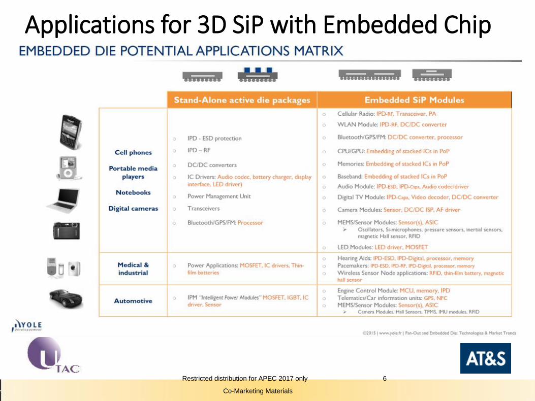
Applications for 3D SiP with Embedded Chip
Co-Marketing Materials
Restricted distribution for APEC 2017 only 6

Embedding Technology Milestones
Concepts Development Projects Industrialization Serial Production Research
2000 2002 2004 2006 2008 2010 2012 2014 2016
Printed resistor
Printed capacitor
Discrete resistor
Discrete capacitor
Embedded silicon
1970
Embedded Chip
Co-Marketing Materials
Restricted distribution for APEC 2017 only 7

Why Chip Embedding?
Unique Selling Propositions … in detail
Miniaturization • Footprint reduction • Higher component integration (additional assembly layer)
Electrical performance • Improved signal performance (higher data rates) • Reduction of parasitic effects
Mechanical performance
• Higher durability and reliability through copper-to-copper connections (copper filled microvias)
• Package enables protective enclosure • High drop, shock and vibration tolerance
Thermal management • Improved heat dissipation through direct copper connection • Improved heat dissipation FR4 versus air (compared to SMD)
Additional functions Reduction of overall cost EMI shielding
• EMV shielding (partial or full shielding of a package) • Package is the housing no additional molding required
ECP is supporting the trend towards modularization
• Lower set-up costs compared to other packaging technologies (packaging versus PCB processes)
• Customization of footprint and module versions can be done due to digital imaging - no separate tooling necessary (e.g. QFN)
Anti-Tamper and Security • Hidden electronics preventing reverse engineering and counterfeiting
Co-Marketing Materials
Restricted distribution for APEC 2017 only 8

Comparison of Package Area vs. Thermal Resistance
Source: GaN Systems, AT&S IMAPS 2014
Co-Marketing Materials
Restricted distribution for APEC 2017 only 9

Package Inductance Ranking
Source: GaN Systems / AT&S IMAPS 2014
Co-Marketing Materials
Restricted distribution for APEC 2017 only 10

TI MicroSiP™ (Introduced 2011 > 20 products)
Co-Marketing Materials
Restricted distribution for APEC 2017 only 11

TDK’s SESUB Technology shrinks power mgmt section 60% in Blackberry ™ Z10 Phone (2013)
SESUB = Semiconductor Embedded in Substrate
Co-Marketing Materials
Restricted distribution for APEC 2017 only 12

Embedded Chip Technology – adoption accelerating in Power Applications
Embedded Chip
Power Solutions
also from:
General Electric
Schweizer
TDK
Infineon’s embedded chip` DrBlade™
Co-Marketing Materials
Restricted distribution for APEC 2017 only 13

UTAC & AT&S Collaboration
System in a package (SiP) is a strategic focus area for UTAC and
AT&S
3D SiP with Embedded Chip provides integration, size and
performance benefits over 2D planar SiP solutions
3D Embedded Chip technology adoption is accelerating in Power and
High Density Interconnect Applications
Supply chain collaboration for emerging 3D SiP solutions with
embedded chip technology will advanced the technology and provide
full turnkey (FTK) supply solutions for customers.
Flexible business models available to fit to customer requirements
Co-Marketing Materials
Restricted distribution for APEC 2017 only 14
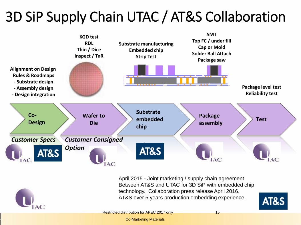
Co- Design
Wafer to Die
Substrate embedded chip
Package assembly
Test
SMT Top FC / under fill
Cap or Mold Solder Ball Attach
Package saw
KGD test RDL
Thin / Dice Inspect / TnR
Substrate manufacturing Embedded chip
Strip Test
Package level test Reliability test
Alignment on Design Rules & Roadmaps - Substrate design - Assembly design
- Design integration
Customer Specs Customer Consigned Option
April 2015 - Joint marketing / supply chain agreement
Between AT&S and UTAC for 3D SiP with embedded chip
technology. Collaboration press release April 2016.
AT&S over 5 years production embedding experience.
3D SiP Supply Chain UTAC / AT&S Collaboration
CMOS driver
Cbyp
GaAs FET die
other passive Components SMT
Co-Marketing Materials
Restricted distribution for APEC 2017 only 15

• Die require 5-10um thick Cu pads for embedding • > 200um pad pitch for yield / cost optimization
UTAC / AT&S 3D SiP Process Flow
Co-Marketing Materials
Restricted distribution for APEC 2017 only 16

3D SiP w/ Embedded Collaboration Example
Package size / Type 4.5 x 7.2 mm LGA-SIP
Substrate Thickness 560 um ± 10% 320um core
Die thickness 200 um Max.
Surface finish (Die DAP) Electrolytic NI/AU
Surface finish (Land Pad) Electrolytic NI/AU
# of Passive Component (Top of substrate surface)
24 Passives
Component Sizes 10ea 01005 10ea 0402 4 ea 0201
# of embedded chip 2
Strip Size 188x64mm
Substrate Metal layers 4 Layer
Package Type: 4.5 x 7.2mm LGA-SIP Highlights: 2 embedded die + 24 passive components on substrate top side
Assembly Layout
Si Die
Co-Marketing Materials
Restricted distribution for APEC 2017 only 17

3D SiP w/Embedded Chip Business Models
1.UTAC provides full turnkey with AT&S as strategic supplier for embedded chip in substrate. Customers place 1 PO to UTAC -full responsibility for quality. Since embedding is a chips 1st process KGD supply is critical to yield. Customers consign wafers. Substrate design complexity has yield complexity so Yield ranges need to be agreed based on KGD quality level and embedded substrate density / yield.
2.AT&S provides FTK with UTAC as strategic supplier for wafer to die processing, assy / test.
This applies where customer is better fit for AT&S due to level of current biz relations. AT&S and UTAC have guides in place and discuss in good faith who best positioned to serve a customer requiring FTK. Above items still apply.
3.Split business with customer providing a PO to AT&S for embedding and UTAC for assy / test.
This model often applies in development phase, but in some cases may apply for production.
In some cases a 3 way NDA may be executed to enable AT&S, UTAC and customer to exchange confidential information to enable Co-design to optimize a design for: Performance, Cost, Reliability, Test and Mfg yield
Co-Marketing Materials
Restricted distribution for APEC 2017 only 18

Summary
System in a package (SiP) is a strategic focus area for UTAC
and AT&S
3D SiP with Embedded Chip provides integration, size and
performance benefits over 2D planar SiP solutions
3D Embedded Chip technology adoption is accelerating in
Power and High Density Interconnect Applications
Supply chain collaboration with AT&S for emerging 3D SiP
solutions with embedded chip technology will advanced the
technology and provide full turnkey (FTK) supply solutions for
customers.
Co-Marketing Materials
Restricted distribution for APEC 2017 only 19

Follow Ups:
Mr. Lee Smith - [email protected]
Mr. Rainer Frauwallner - [email protected]
Co-Marketing Materials
Restricted distribution for APEC 2017 only 20