π/4 dqpsk transmitter and receivermicrowave.ee.cuhk.edu.hk/files/ads_notes/dqpsk.pdf ·...
TRANSCRIPT

Microwave Laboratory ADS Application Notes Page 1
ππππ/4 DQPSK Transmitter and receiverLo Kwok Leung Carlo
Sept. 15, 2001
AbstractThe objective of this project is to provide students a hand on experience of the HPADS
software. The goal is to build a DQPi/4PSK transmitter and receiver.The reference design of the transmitter was given for student to practice the schematics
capture and the simulation techniques. Then the students are required to design and buildthe simulation model for the receiver.
The transmitter and receiver were built and the eye diagrams, constellation diagramdiagram were recorded.
Three types of channel were tried and the bit error rates were recorded and plotted.
The SystemThis is the system diagram of the overall testing system. The small block on the left is the
transmitter. There are two signal paths. The upper path simulates a normal RFcommunication path. The lower path connects the original baseband data to the BERcalculator for system evaluation.
Illustration 1 The Overall System
ADS Application Notes
Microwave Laboratory, Department of Electronic EngineeringThe Chinese University of Hong Kong
Microwave Laboratory ADS Application Notes Page 2
The Upper Path:The block with an antenna icon and that with a noisy waveform function as the channel.
Three different channels were simulated and would be described in the Result section. Therectangular block is the receiver which converts RF signals into base band data.
The Lower Path:The output of the transmitter on the lower path is the direct output from the data_source
unit. The data content is exactly the data before all modulation and RF channeling. It acts asthe reference data for bit error rate calculation. The data first pass through a delay block tocompensate the delays for all the modulation, conversion and RF channel on the upper path.Then the signal is amplified to a signal level close the received data. At the end, the datafrom both paths are compared at the BER block. Hence the system performance is qualified.
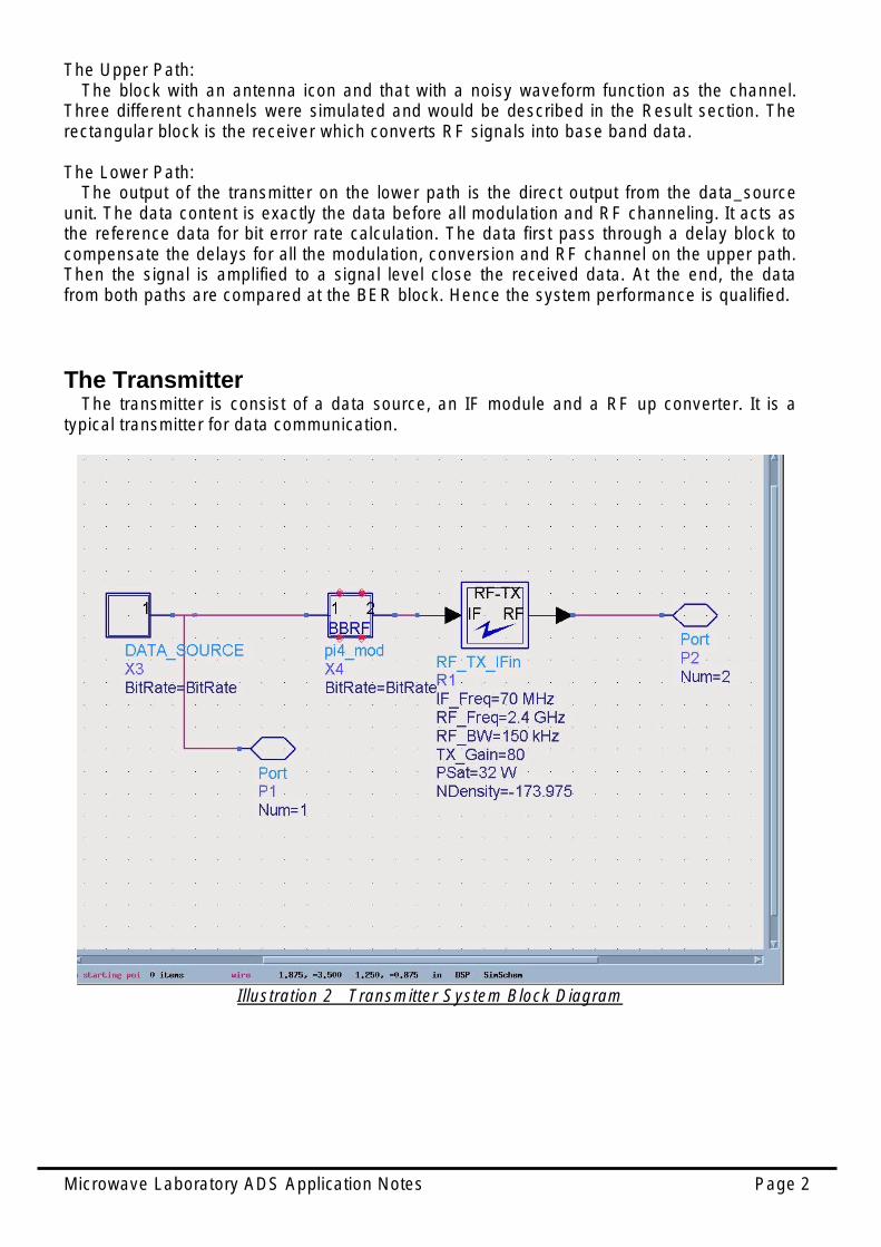
The TransmitterThe transmitter is consist of a data source, an IF module and a RF up converter. It is a
typical transmitter for data communication.
Illustration 2 Transmitter System Block Diagram

Microwave Laboratory ADS Application Notes Page 3
The data source:The data source module consists four building blocks: The random bit generator, the
LogicToNRZ, the FloatToTimed and the UpSampleRF. The random bit generator generatebit stream of one and zero according to the distribution defined. Given long enough time, allpossible bit pattern would be tried. The LogicToNRZ is a block to convert logic signal of "0"and "1" into floating point number of "-1" to "1". It is a normal practice to convert logic signalto NRZ signal to avoid biasing subsequence circuit with a DC residuals.
Illustration 3 The Transmitter System
Illustration 4 Data format of NRZ
Then the floatToTimed block converse the floating point number into a time based signalfor simulation purpose. The UpSampleRF element over sample the bit stream for simulationpurpose.
Microwave Laboratory ADS Application Notes Page 4
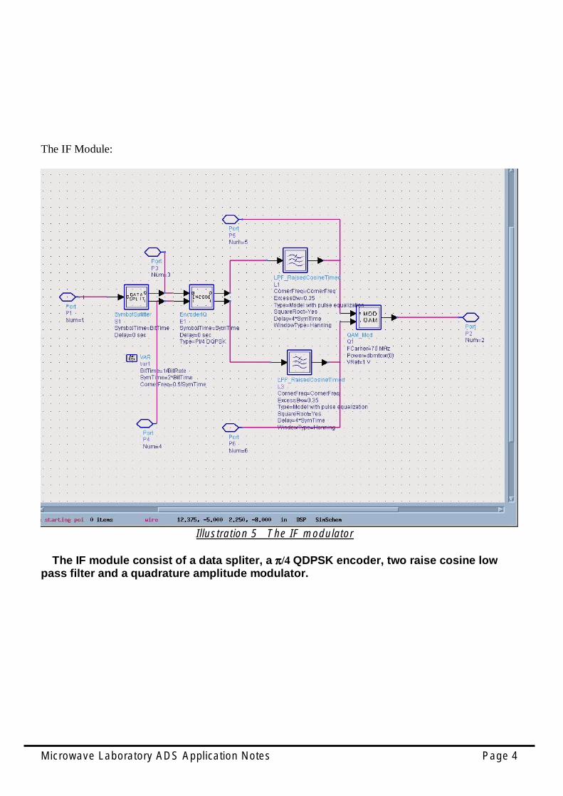
The IF Module:
Illustration 5 The IF modulator
The IF module consist of a data spliter, a ππππ/4 QDPSK encoder, two raise cosine lowpass filter and a quadrature amplitude modulator.

Microwave Laboratory ADS Application Notes Page 5
Illustration 6 Data Splitter Output
The function of the data splitter is to do a serial to parallel conversion. It takes in two bitsfrom the serial input and output them into I and Q channel. The first bit would be put into the Ichannel and the second bit would be put into the Q channel. There is a constant delay of twobits time. So, the I and Q channel are only valid after two bit duration. Here is a plot for theoutputs of the data splitter. Here the bit time is set to 0.1ms for the ease of understanding.Note the red color trace represent the input data and the blue traces represent the I and Qdata outputs.
For each of the data channel, data are modulated in π/4 DQPSK modulator. PSKmodulation is a commonly used technique. It has the benefits of constant envelop and highfrequency efficiency. The "D" in DPSK means the coding is a differential coding. It encodesthe difference between the current input with the delayed output. The aim of application ofDPSK is the recovery of phases without the need for the exact phase of the carrier. In orderword, non-coherence detection can be carried out.Then the Raise Cosine LPF is used to do a pulse shaping. All higher harmonics would beattenuated. The use of Raise Cosine filter is to reduce the possibility of ISI due to limitedbandwidth.
The Raise Cosine output needed to be converted into the intermediate frequency. TheQAM encoder accepts the IQ input and modulates the IF in amplitude modulation format. Butthe HPADS would not simulate the high frequency carrier. So, only the information forbaseband could be seen. Here is a plotting of the real part and imaginary part of the QAMoutput. Note, the real part co-responding to the I channel and the imaginary part co-responding to the Q channel.

Microwave Laboratory ADS Application Notes Page 6
Illustration 7 The I & Q modulation Input/Output
By plotting the I and Q channel data on the X-Y plot, the constellation diagram is formed.Here are the constellation of the π/4 DQPSK output and the QAM input.

Microwave Laboratory ADS Application Notes Page 7
Here is a graph showing the eye diagram of the QAM output:
The IF-RF module:It up convert the IF signal into RF band. The current configuration is to up convert the IF of
70MHz into 2.4GHz.
The ReceiverThe receiver consists of a RF to IF converter, a QAM demodulator, 2 Raise Cosine LPF, a
π/4 DQPSK decoder and a data combiner. In short, it is a reciprocal design of the transmitter.
Illustration 11 The Receiver Design

Microwave Laboratory ADS Application Notes Page 8
The RF-IF module downconvert the RF signal of 2.4GHz into 70MHz IF. Then, the QAMdemodulator demodulates the IF QAM signal back into IQ data. The filters do the pulseshaping. Then the DPSK demodulator demodulates the signal into IQ digital data. Finally, thecombiner recombines I and Q digital data back into baseband signal.
System QualificationThe system qualification is performed by the BER block. This block accept two data input
channels, then synchronize and normalize them. Then a comparison is made and the rate ofmismatch is calculated.
Illustration 12 The BER block

Microwave Laboratory ADS Application Notes Page 9
Here is a plot of the display for received data, transmitted data and the resultant BER.
Illustration 13 The Received Data, Transmitted Data and the Resultant BER
ProceduresThe transmitter was built according to the project instruction.The constellation diagrams and eye diagram were plotted to confirm the transmitter
performance.Then the receiver was built by adding components one at a time. Before adding a
component, experiment was carried out to examine the function of it. In the same time, thedelay time required for synchronization were tested.
The data combiner was connected to the data splitter. It was found that after 4 bit time, thereconstructed data synchronize with the source data.
The π/4 DQPSK modulator and demodulator were added in between the data splitter andcombiner. The data were found reconstructed correctly. (The delay time was not recorded.)
The LPF, QAM modulator and demodulator were added in between the π/4 DQPSKmodulator and demodulator. Data ware reconstructed.The IF-RF and the RF-IF blocks were inserted in between the QAM modulator anddemodulator. The data were reconstructed. The overall delay was found 24 bits time.
The BER block was added to compare the data from the data source and the receiver.Different channels were insert between the IR-RF and RF-IF blocks.Simulations were carried out according to different parameter setting.

Microwave Laboratory ADS Application Notes Page 10
ResultsThree types of channels were tried:
1. Antenna with different gain and noise density.2. 2. Mobile Channel.3. 3. Mobile Channel with two antennas.
1. Antenna with different gain and noise density:In this experiment, the BER for different gain and noise density combination were
measured. The gain means the channel gain. The noise density measures in dbm/Hz. Thenormal thermal noise is at -174dbm/Hz. The higher the value means the higher thetemperature.

Microwave Laboratory ADS Application Notes Page 11
Here are the results Bit Error rate at different noise density according to different antennagain. The BER increases with noise density and decrease with the channel gain.
Illustration 14 BER vs Noise Density @ different channel gain
2. The Mobile Channel:
The GSM mobile channel simulates multipath delay, fladding and path loss. The mobileantenna simulates distance from the source and the velocity of the mobile.
The Bit Error Rate at two mobile velocities were simulated. The distances from the sourceranged from 1Km to 100Km. Here is the result.
The BER increase with distance at the first 15Km. After a peak value, the BER ranges 0.46to 0.48. The peak BER for higher mobile velocity is higher. The location of the peak locatesat a larger distance for the higher velocity.

Microwave Laboratory ADS Application Notes Page 12
Illustration 15 BER vs Distance @ 2 velocities

Microwave Laboratory ADS Application Notes Page 13
3. Mobile Channel with two antennasThis objective of this arrangement is tried to check if diversity helps to improve the BER.
An extra propagation path and antenna is added. The x-position and speeds of the twomobile antennas are identical. But the y-position of the first antenna is kept at 5m alwaysfrom the other. The RF splitter is used to split the RF signal into two paths. The RF summersums up the signal received and feeds the output to the receiver.
Here is the result obtained. The velocity of both mobile antennas are set to 100m/s.
Illustration 16 BER vs Distance for 1 and 2 antenna condition
It is quite surprise to see the BER for the 2-antenna case is higher than the 1-antennacase. At the frequency of 2.4GHz, the wavelength is 12.5cm. A distance of 5 meter should belong enough for a diversity setup. Hence the model built here may not really simulating thediversity situation.

Microwave Laboratory ADS Application Notes Page 14
ConclusionTechniques were learnt how to build a simple TX and RX system.Three different kinds of channel were tested.HPADS is a good tool for both system level and board level simulations.Information and documentation is not sufficient for users to fully appreciate the power of it.