400g - looking forward to 800g and terabit speedsb4) 400g... · 2019-05-31 · • ieee...
TRANSCRIPT

Senior Project Manager / Keysight Technologies
Joe Lin
400G: Looking Forward to 800G and Terabit Speeds

2
• Introduction
• PAM4 Simulation
• 400G -> 800G Measurementso Direct Detect Output (Transmitter) Testo Direct Detect Input (Receiver) Testo Coherent Optical Testo Layer 2-3 Analysis
• Summary
Keysight World

3
Metro-Telecom Metro-DCI
Server
Core Network Data Center
Intra-DC
Network
Longhaul/
undersea
100 km – 39,000 km
60 mi – 24,000 mi
10 km – 100 km
6 mi – 60 mi
20 m – 10 km
22 yd – 6 mi
1 mm – 3 m
.04 in – 10 ft
10 km – 40 km
6 mi – 25 mi
DCI
Inter-DC Intra-DC
Coherent
How low can you go? NRZ / PAM4
How far can you go??
Keysight World

4
E N A B L E S H I G H E R D ATA T H R O U G H P U T
• NRZ > 28 Gb/s limits trace length or increases cost
• PAM4 yields 2 bits / symbol
✓ Effectively halves the channel BW needs
• Allows designers to develop products to fit the cost
structure of available channel technologies.
• PAM4: Pulse Amplitude Modulation 4-level
• 2 bits of information in every symbol
✓ ~ 2x throughput for the same baud rate
✓ 26.56 Gbaud PAM4 = 53.125 Gb/s
• Lower SNR, more susceptible to noise
• More complex Tx/Rx design, higher cost
Keysight World

5
✓
✓
✓
✓
✓
• OIF-CEI-56G Released
5 reaches PAM4 up to 29 Gbaud, NRZ up to 58 Gb/s
• IEEE 802.3bs 200/400G (Ethernet) Released
Medium reach SMF + C2C,C2M, PAM4 @ 53.1 & 26.6 Gbaud
• IEEE 802.3cd: 50/100/200G (Ethernet) Released
Short reach MMF. + C2C,C2M, backplanes & cables, PAM4 @26.6 Gbaud
• 64G Fibre Channel Complete, pending publication
100m – 2 km reaches in MMF & SMF, PAM4 @ 28.9 Gbaud
• COBO version 1.0 Released
(Optical PHY from 802.3bs, Elec. from OIF-CEI-56G-VSR)
• IEEE 802.3cm 400G Under development
Short reach in MMF, PAM4 @ 26.6 Gbaud
• IEEE 802.3cn 50/100/200/400G Under development
10 km SMF, PAM4
• OIF 400ZR Under development
80 km SMF, DP-16QAM @ 60 Gbaud, coherent
• IEEE 802.3ct 100/400GBaseZR Under development
80 km SMF, DP-16QAM, coherent, (based on OIF 400ZR)
Keysight World
C U R R E N T G E N E R AT I O N - 5 0 G L A N E R AT E

6
• OIF CEI-112G Project starts for 5 reaches,
5 reaches PAM4, CNRZ-5 C2M at 7th draft
• IEEE 802.3ck First baseline draft for C2M May2019
C2M & C2C for 2nd wave 400GbE & 800G (based on OIF CEI-112G-VSR, MR, and LR)
• Fibre Channel PI-8 128GFC Project Start
Moving closer to Ethernet baud rate
Keysight World
11 2 G L A N E R AT E S
7
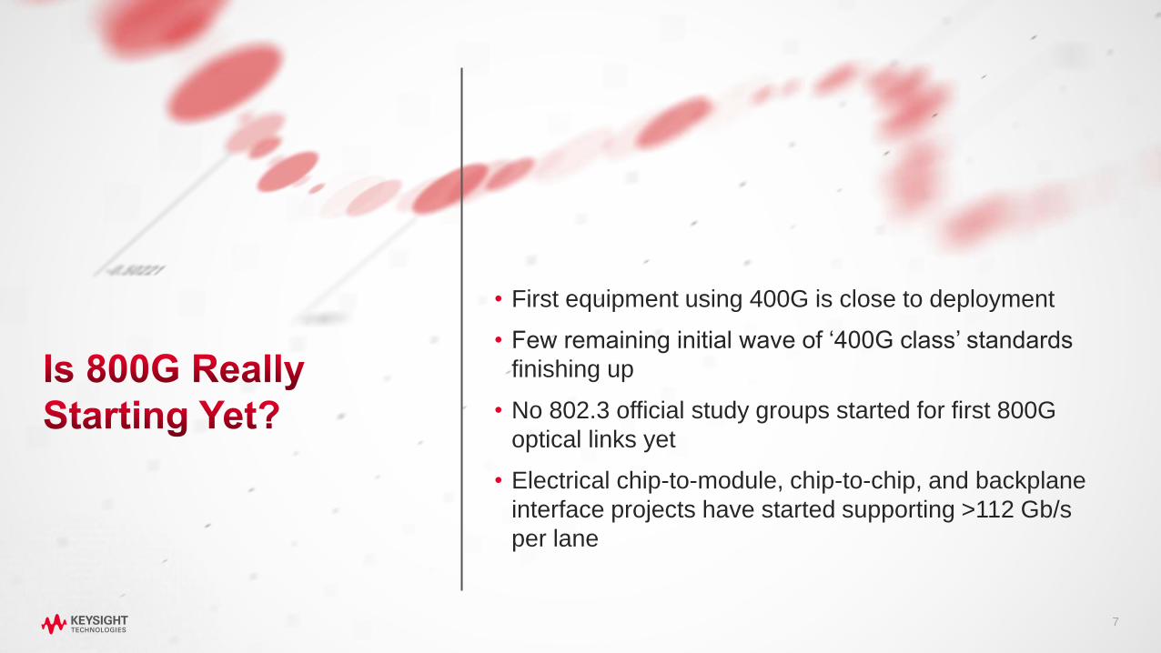
• First equipment using 400G is close to deployment
• Few remaining initial wave of ‘400G class’ standards
finishing up
• No 802.3 official study groups started for first 800G
optical links yet
• Electrical chip-to-module, chip-to-chip, and backplane
interface projects have started supporting >112 Gb/s
per lane

8
• Optical – 56 Gbaud PAM4 – Proven in 400GBASE-DR4 (part of 802.3bs)
• Electrical – mostly 56 Gbaud PAM4
• Most (but not all) detectors will digitize with DSP
• Optical and electrical links continue to rely on FEC to restore error free link
• FEC will pass through and not processed in module
• Will there be a 224G C2M AUI?
• Not without higher bit/symbol modulation. Some multi-wire modulations are being studied.
Keysight World

9
E N D - T O - E N D S O L U T I O N S F R O M K E Y S I G H T
400G
Design
Cycle
Channel/ Interconnect
Receiver Test
M8194A AWGM8040A BERT
N1000A DCA-X / N1092A DCA-M
Sampling Scope
UXR Real-time Scope
PLTS + M980Xa VNA
L2/L3 400GE Test
Modeling / Link Simulation
Transmitter Test
ADS, FlexDCA link
ARESONE-400GE
Keysight World

10
PAM4 Simulation

11
Transmitter
(IC)Channel
Receiver
(IC)
E X A M P L E : 4 0 0 G C H I P - T O - C H I P ( C 2 C ) T E S T B E N C H S E T U P
Keysight World
DFE
enabled
C2M Components
– Host Board
– Connector
– SMA Cables
• Keysight ADS SW provides comprehensive PAM4 Channel Simulation Analysis using vendor IBIS-AMI models
• Test Setup: TP0 to TP5 (ball-to-ball)
IBIS (IO Buffer Info Specification)
AMI (Algorithmic Modeling Interface)http://www.eda.org/ibis/

12
A D S 2 0 1 9 T O F L E X D C A “ C O N N E C T E D F L O W ”
Keysight World
ADS
Simulation Domain DCA-X Oscilloscope
Measurement Domain
Compliance Apps
FlexDCA – Eye/Jitter Analysis
• Connects simulation and measurement domains seamlessly: “Design to Test”
• Uses the same measurement algorithm and methodology on both simulated and measured waveforms
• Expands ADS PAM4 measurement capabilities to include Jitter analysis and TDECQ
• Runs compliance apps on simulated and measured waveforms

13
PA M 4 , J I T T E R , C O M P L I A N C E A P P S
Keysight World
• ADS starts FlexDCA automatically
• Unlock all built-in comprehensive PAM4 analysis in FlexDCAo Eye contour
o TDECQ (Transmitter Dispersion Eye Closure Quaternary)
o Outer OMA
o Linearity
o Noise Margin
o Partial SER
o Partial TDECQ
o Levels, Level Skews
o Eye Skews, Height, and Width..
• Jitter Analysis
• Run Compliance Apps
Jitter Analysis
ADS Waveforms -> FlexDCA
Math and DSP in FlexDCA

14
Direct Detect Output
(Transmitter) Test

15
I E E E 8 0 2 . 3 B S E L E C T R I C A L T X T E S T P O I N T S
Chip-to-Chip (C2C) at TP0a
(custom fixture)
Chip-To-Module (C2M) at TP1a
(use compliant fixture)
C2C
C2M-HostC2M-Module
Chip-to-Module Module Output (C2M) at TP4
(use compliant fixture)
Keysight World

16
• Baud rates continue to increase (from 26 to 53 Gbaud)
oStandards (IEEE 802.3bs/cd, CEI 4.0,...) require:✓ higher bandwidth test equipment
✓„ideal“ 4th Order Bessel-Thomson reference receiver response
✓equalization to open signals for analysis
• Degraded PAM4 Eyes
oRequires low noise reference receivers and
advanced clock recovery
• Complex New Measurements
oRequires advanced analysis tools
N E W A N A LY S I S M E T H O D O L O G Y R E Q U I R E D T O A N A LY Z E D E G R A D E D S I G N A L S
Keysight World

17
Receiver Frequency Response:
4th Order Bessel-Thomson (BT) Response
Typical RT
“Brick wall”
Response
Typical SS Response
Scopes have different frequency responses:
➢ Will result in different eye/waveform shapes and amplitudes
–> different measurement results
Examples (26 Gbaud PAM4; 53 Gb/s):
• IEEE 802.3bs™/D3.5 (Ethernet)
Clause 120D.3.1 200GAUI-4 or 400GAUI-8 transmitter characteristics:
“A test system with a fourth-order Bessel-Thomson low-pass response with 33
GHz 3 dB bandwidth is to be used for all transmitter signal measurements,
unless otherwise specified.”
To provide more measurement consistency, most standards now specify BW and shape.
• CEI-56G-VSR-PAM4
Section 16.3.4 Output Differential Voltage, pk-pk
“The waveform is observed through a fourth-order Bessel-Thomson response
with a 3-dB bandwidth of 40 GHz using a QPRBS13-CEI pattern.”
Step Response (red)
Frequency Response (blue)
➢ To achieve 33/40 GHz 4th Order BT response on a RT scope,
must start with > 60 GHz “brick wall” response
Keysight World

18
• 43 GHz Bessel response is deemed to be
representative of “112G” transmitters
(chip -> package -> fixture)
• Will this be sufficient BW for Tx
characterization? Will 43 GHz BW penalize
(reduce EH/EH margins) designs with better SI
performance?
P R O P O S E D 4 3 G H Z B E S S E L
Keysight World

19
Clock recovery (CR)
• Recovers a clock for the Rx to use in real systems
• Scopes need to emulate CR used in real Rx
(track out low-frequency jitter, trigger the scope)
PAM4 adds complexity
• Transitions no longer only at 0V diff
• CR Loop BW reduced from 10 MHz to ~ 4 MHz
(IEEE 802.3bs/cd and CEI-56G-PAM4, same for 112G standards)
Instrument clock recovery
• Real-time oscilloscopes use software CR
• Equivalent-time oscilloscopes (aka Sampling scopes) use hardware CR
• CR needs to be able to lock onto “closed eyes”
Keysight World

20
H I G H E R C H A N N E L L O S S , X TA L K , A N D R E F L E C T I O N S AT 5 3 G B A U D ( 1 0 6 G B / S )
Step 1: Scope must obtain CR lock (SW or HW) in
order to analyze/equalize signals
o Ensure the CR in your instrument can lock onto
severely closed eyes
Step 2: Equalize the signal and analyze
o “56G” Today: only uses CTLE (up to 9 dB)
o “112G” Future: will likely require a combination
of CTLE, FFE (5 tap?, 12 tap?), and/or DFE
53 GBd PAM4 signal via channel with
16 dB loss at 26 GHz (Nyquist).C2M Channel Insertion Loss (IL): Up to 16dB at 26.56 GHz (proposed).
Whole link insertion loss can be more than 20dB.
Keysight World

21
K E Y PA M 4 M E A S U R E M E N T S F O R E L E C T R I C A L T R A N S M I T T E R S
• Eye Width (EW), Eye Height (EH)
• Eye Symmetry Mask Width (ESMW)
• Output waveform
oLevel Separation Mismatch Ratio
• Signal-to-noise-and-distortion ratio
(SNDR)
• Output jitter
oJRMS
oJ3u, J4u
oEven-Odd Jitter (EOJ) While these parameters may
sound familiar to you, they
are measured very differently
compared to legacy NRZ
designs
Keysight World

22
• Output Jitter parameters for Tx:o J3u (e.g. IEEE 802.3cd)
o J4u (e.g. IEEE 802.3bs and CEI-56G-MR/LR)
o JRMS
o Even-Odd Jitter (EOJ)
• Measured on 12 specific transitions of a PRBS13Q
(IEEE) and QPRBS13-CEI pattern (8191 symbols
long) in order to exclude correlated jitter
• 12 transitions represent all possible combinations of 4
identical symbols followed by 2 different identical
symbolso Captures any jitter issues in Tx design
M E A S U R E J 3 U , J 4 U , J - R M S , E V E N - O D D J I T T E R
Keysight World
8191 symbols
Use data from only 12 edges
Example:
• R03 = 10000 330
1
0 0 0 0
3 3
0

23
S P E E D A N D R E P E ATA B I L I T Y
• Output Jitter (J3u, J4u, JRMS, and EOJ) can be a very time
consuming measurement
oRequires optimized algorithms
• Requires a very stable and repeatable timebase
o Check for scope repeatability (figure of merit: StdDev)
• AM-to-PM conversion will impact results
oRandom noise (RN) will increase measured jitter as channel loss
increases (edges will slow down).
oExpect an increase in J4u, JRMS as channel loss increases.
• How much data is required for an “accurate” measurement?
oRJ/PJ histogram of > 400k typically samples yields stable results
oHigher channel loss and crosstalk will necessitate more data0
0.005
0.01
0.015
0.02
0.025
0.03
51 52 53 54 55 56 57 58 59
Un
it In
terv
al (U
I)
Baud Rate (GBd)
Output Jitter: EOJ
Spec (19 mUI)
N1000A DCA-X results
Keysight World

24
E N G I N E E R E D F O R T E S T I N G 4 0 0 G / 8 0 0 G D E S I G N S … A N D B E Y O N D
N1000A DCA-X Equivalent-Time “Sampling” Oscilloscope
N1060A Precision Waveform Analyzer (aka “MegaModule”)UXR-Series Real-Time Oscilloscope
Keysight World
25
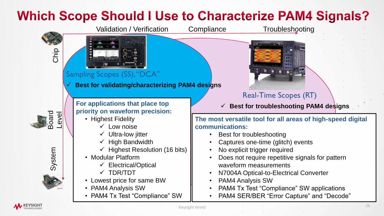
Validation / Verification Compliance Troubleshooting
Chip
Board
Level
Syste
m
Sampling Scopes (SS), “DCA”
✓ Best for validating/characterizing PAM4 designs
Real-Time Scopes (RT)
✓ Best for troubleshooting PAM4 designsFor applications that place top
priority on waveform precision:
• Highest Fidelity
✓ Low noise
✓ Ultra-low jitter
✓ High Bandwidth
✓ Highest Resolution (16 bits)
• Modular Platform
✓ Electrical/Optical
✓ TDR/TDT
• Lowest price for same BW
• PAM4 Analysis SW
• PAM4 Tx Test “Compliance” SW
Keysight World
The most versatile tool for all areas of high-speed digital
communications:
• Best for troubleshooting
• Captures one-time (glitch) events
• No explicit trigger required
• Does not require repetitive signals for pattern
waveform measurements
• N7004A Optical-to-Electrical Converter
• PAM4 Analysis SW
• PAM4 Tx Test “Compliance” SW applications
• PAM4 SER/BER “Error Capture” and “Decode”

26Keysight World
• Outer OMA
(difference between the 3 level and 0 level)
• Outer ER (ratio of 3 and 0 level)
• Rise/fall times (per IEEE 802.3cd)
• Transmitter and dispersion eye closure for
PAM4 (TDECQ)
➢ Replaces mask testing!
➢Requires equalizers and “short patterns”
(SSPRQ…no more PRBS31 for TX test).
• Optical Modulation Amplitude (OMA)
(difference between the 1 level and 0 level)
• Extinction Ratio (ER)
(ratio of 1 and 0 level)
• Transmitter Dispersion Penalty (TDP)
• Eye-mask
NRZ Transmitters

27
• Tells you the performance of your transmitter relative to an ideal transmitter
• For NRZ TDP, we literally used a BERT to measure the BER performance of the transmitter
compared to an actual golden transmitter
➢ Determine how much extra power was required at the receiver to compensate for non-ideal performance
• For TDECQ we indirectly measure SER (symbol error rate) using a scope, no BERT required
T R A N S M I T T E R D I S P E R S I O N A N D E Y E C L O S U R E Q U AT E R N A R Y
Keysight World

28
• SSPRQ test pattern (216-1 length)
• Includes test fiber dispersion (single-mode)
• Oscilloscope noise measured and
mathematically ‘backed out’
• Apply TDECQ equalizer
oVirtual 5 tap, T spaced FFE reference
equalizer (EQ taps optimized to minimize
TDECQ penalty)
• Histograms constructed to assess eye closure
relative to OMA and compute an effective power
penalty in dB. This is the TDECQ result.
(note: a smaller number is better)
F R O M I E E E 8 0 2 . 3 B S
Keysight World

29
N1092A/B/D “DCA-M”
• 26/53 GBd Optical Ref Rx
• Multimode and Single-Mode
• 1, 2, or 4 channels
• Low-noise receiver
• PAM4 analysis with TDECQ
Optical
DUT
N1092A/B/C/D 26/53 GBd Optical Reference Receiver
N1077A 32 GBd Optical Clock Recovery
Recovered
Clock
N1078A 64 GBd Optical Clock Recovery
• Includes internal variable equalizer
(open “closed” eyes)
N1092x with Optical Clock Recovery
New
FlexDCA User Interface:➢Integrated PAM4 measurements
results in FAST, EASY and
COMPLIANT measurements
New
F U L LY C O M P L I A N T F O R A L L O P T I C A L PA M 4 A P P L I C AT I O N S
Keysight World

30
Direct Detect Input
(Receiver) Test

31
• Measurement challenges for 56 Gbaud (112 Gb/s) Rx characterization
o Links do not run error free (by design) - Avoid use of loopback to BERT ED
o New reference receiver
Keysight World

32
• The Bit Error Ratio Tester (BERT) will continue to be the principle tool for input testing
BERTPattern
Generator
DUT
Rx
INTx
OUT
ChannelBERTPattern
Generator
BERT
Error
Detector
“Stressed”
Data Pattern
Clean Loopback
Link
Traditional BERT input test setup
Determine ability of DUT’s Input to correctly receive impaired data
Clean loopback link required to prevent adding errors at BERT ED input
• Will the loopback path be error free in links designed to use FEC for error free operation?
Keysight World
Receiver output to be
tested inside the DUT
33
S A M E T E S T U S E D I N L E G A C Y M O D U L E S ( N R Z )
1. BERT PG + ISI channel provides
stress signal to Tx input
2. Stressed signal drives optical Tx
output through TOSA elements
3. Fibre patch cable provides
loopback to optical Rx input of
same or second (“golden”)
module to serve as O/E
4. Looped back signal routed to
BERT ED
Frequency
Dependent
Attenuator
Module Compliance
Board
Module under test
Rx
Tx
TOSA
ROSA
Tx input being tested
Required BER for CAUI-4 C2M link: 1E-15, tested to 1E-12 (Error free)
Required BER for entire link (C2M + Optical): 1E-12 (Error free)
Example: 100GBASE-LR4, Tx input (electrical) test, each lane tested independently
PG
ED
BERT
Keysight World
34
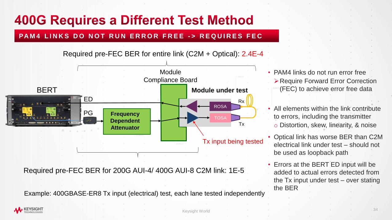
PA M 4 L I N K S D O N O T R U N E R R O R F R E E - > R E Q U I R E S F E C
• PAM4 links do not run error free
➢Require Forward Error Correction
(FEC) to achieve error free data
• All elements within the link contribute
to errors, including the transmitter
o Distortion, skew, linearity, & noise
• Optical link has worse BER than C2M
electrical link under test – should not
be used as loopback path
• Errors at the BERT ED input will be
added to actual errors detected from
the Tx input under test – over stating
the BER
Frequency
Dependent
Attenuator
Module
Compliance Board
Module under test
Rx
Tx
TOSA
ROSA
Tx input being tested
Required pre-FEC BER for 200G AUI-4/ 400G AUI-8 C2M link: 1E-5
Required pre-FEC BER for entire link (C2M + Optical): 2.4E-4
Example: 400GBASE-ER8 Tx input (electrical) test, each lane tested independently
PG
ED
BERT
Keysight World
35
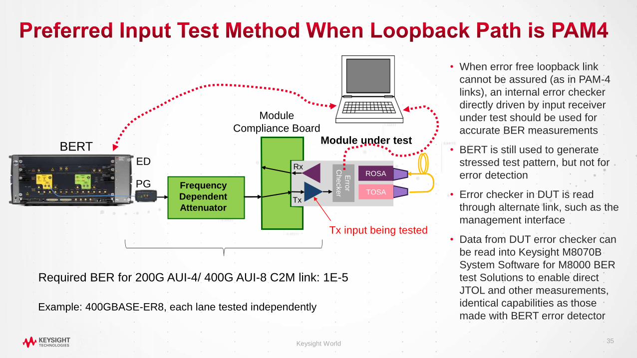
Module
Compliance BoardModule under test
Rx
TxTOSA
ROSA
• When error free loopback link
cannot be assured (as in PAM-4
links), an internal error checker
directly driven by input receiver
under test should be used for
accurate BER measurements
• BERT is still used to generate
stressed test pattern, but not for
error detection
• Error checker in DUT is read
through alternate link, such as the
management interface
• Data from DUT error checker can
be read into Keysight M8070B
System Software for M8000 BER
test Solutions to enable direct
JTOL and other measurements,
identical capabilities as those
made with BERT error detector
Tx input being tested
Required BER for 200G AUI-4/ 400G AUI-8 C2M link: 1E-5E
rror
Ch
ecke
r
Example: 400GBASE-ER8, each lane tested independently
Frequency
Dependent
Attenuator
PG
ED
BERT
Keysight World

36
• Use of internal error checkers eliminates degraded BER measurements from loopback path errors
oPRBS31Q (same as OIF QPRBS31-CEI) is the standard test pattern for C2M compliance input testing
• If chip density does not allow internal error checker, consider adding PRBS-Q pattern generator
oPattern generator provides means to measure BER in loopback path only, isolated from receiver under test
Keysight World
DUT
Rx
IN
Tx
OUT
BERTPattern
Generator
BERT
Error
DetectorTest
Pattern
Generator

37
• The “Reference Receiver’ normalizes the signal conditioning front end in test instruments used for
Output (Tx) measurements and Input (Rx) stressed eye calibration
• Reference receiver is supposed to emulate a generic receiver implementation with minimal
performance required to close the link budget
Reference: OIF CEI-112G-VSR Figure 23-10 Module Input Test Setup Draft ver. 07
Keysight World

38
• Problem – measurement instrument may “see” artifacts in the link signal that will
not impact the receiver
• e.g. higher frequency components beyond receiver bandwidth
• Solution – add a “Reference Receiver” to constrain measurement to signals as
seen by actual receiver
• Removes out of band noise, DC from measurement
• Accuracy required for measurement repeatability
Keysight World
Why is the Reference Receiver Needed?
Transmitter Receiver
Reference
Receiver
Measurement
Instrument

39
• Accurate measurement of what the DUT is seeing, results when reference receiver uses this
approximation:
• Where HDUT par.(X) is the actual receiver response to the parameter being measured
• e.g. receiver’s BW emulated by LPF in reference receiver
Keysight World
The Reference Receiver
HDUT par.(x) = HRef.Rec.(x)
Transmitter Receiver
Reference
Receiver
Measurement
Instrument

40
Reference Receiver
Topology: (specified: Bessel-Thompson)
Roll Off: (specified :4th order)
Frequency: (specified – 3 dB @ 43 GHz)
Gain: (specified: 3.0)
LPF
“Tune for Best Response”
Keysight World
• Traditionally, operational parameters of signal conditioning in front of test instrument are tightly specified for
repeatable measurements
• Optimizing equalizer (“Tune for best response” )
• OK for receiver, but challenges measurement repeatability
• Example – self optimizing equalizer gives 50% UI EW in one case, with same Tx and channel, 58% in another.
Fine for a real receiver, but not a measurement instrument ! (16% difference in EW measurements)

41
CEI 112G/ 802.3ck Reference Receiver
• Cascaded equalizer – CTLE + FFE and possibly DFE
• All stages are self optimizing
Keysight World
Specified Parameters:
• Number of taps
• Cursor position
• Tap weight range
• Tap weight increment
Select from table
of DC gains
Specified Parameters:
• Number of taps
• Tap weight range
CTLE FFE DFE
Measurement
Instrument

42
In theory optimizing equalizers could be used in reference receivers and give repeatable
measurements when these conditions are met:
• Order of placement of equalizer elements (CTLE first, followed by DFE or FFE, followed by ___)o Linear systems should allow interchanging, but this ignores action of noise on individual equalizer elements
• Tap configurationoCursor placement
o Lange limits
o Increment step size
• Optimization stop criteria
• Will actual implementations follow theory and be repeatable?oConcern with recent example – TDECQ measurement (output Tx output in 400G 802.3cd standard project)
o TDECQ algorithm required several draft iterations to address non-repeatability between instrument vendors and poor correlation with BER results
o Large cause was found in self-optimizing TDECQ equalizer (FFE), and Ref RX model was not representative of actual RX
Keysight World

43
Coherent Optical Test

44
C O H E R E N T V S D I R E C T D E T E C T I O N : A C O S T A N D P O W E R G A M E
Direct Detection (PAM4)Cost
Power / Size
Latency
Needs CD compensation depending on link length
Bandwidth (DWDM): 4 Tbit/s
CoherentCost
Power / Size
Latency
DSP compensates CD adaptive to link length
Bandwidth (DWDM): 20 / 30 Tbit/s with 16 / 64QAM
Being addressed through
reducing DSP requirements
and moving to 7 nm CMOS
Source: Acacia Inc.
Keysight World

45
G R A P H I C A L R E P R E S E N TAT I O N
I
(in-phase
or
real part)
Q (quadrature or imaginary part)
1
0I
(in-phase
or
real part)
Q (quadrature or imaginary part)
Q
value
I value
01 11
0010
Phase
F
1) Information is in amplitude
2) Phase can be random1) Information is in amplitude
2) Information is in phase
Keysight World

46
This is the region of
transition between
symbols
This is the region where the
symbol/vector state should be
stable and where communications
quality is assessed
I (in-phase,
real part)
Q (quadrature,
imaginary part)
QPSK constellation map
11
00
01
10
I
Q
Need amplitude AND phase
sensitive measurement!
Keysight World

47
OOK (NRZ / PAM4)
• Q-factor
• Eye mask (NRZ)
• TDECQ (PAM4)
• Timing jitter
• BER
• OSNR
Complex Modulation
• EVM
• IQ Imbalance, IQ Offset
• Quadrature Error
• Frequency Offset
• BER
• OSNR
Keysight World

48
✓ Global quality metric for coherent Tx
• Needs reference receiver comprising
• Calibrated optical front-end
• Real-time ADC
• Defined signal processing blocks
Q U A L I T Y M E A S U R E F O R C O M P L E X M O D U L AT E D D ATA S I G N A L S
Measured
constellation
pointI (in-phase,
real part)
Q (quadrature,
imaginary part)
Phase φ
Reference
constellation
pointError vector
𝐸𝑉𝑀𝑟𝑚𝑠 =
1𝑁σ𝑛=1𝑁 𝐸𝑉𝑀 𝑛 2
𝑝𝑒𝑎𝑘 𝑟𝑒𝑓. 𝑣𝑒𝑐𝑡𝑜𝑟
The Error Vector connects the measured vector and the reference vector!
An Error Vector = 0 means we have an ideal signal!
Keysight World

49
Proposed reference receiver for coherent transmitter testing:
• Dual-polarization coherent receiver
• Real-time signal acquisition (four synchronized ADC channels)
• Frontend correction
• Digital signal processing
A D D I T I O N A L I M PA I R M E N T A N A LY S I S F E AT U R E S
Reference receiver HW & SW
characteristics need to be
specified for the development
of an EVM specification
Keysight supports these efforts in:
M8290A
✓ Optimized for up to 400G signals
✓ Most compact
✓ Most affordable
✓ 4ch. 92 GSa/s
✓ 40 GHz
✓ 512 kSa memory
Keysight World
Pol. Div.IQ Mixer
ADC
ADC
ADC
ADC
Frontendcorrection
Digital Signal Processing,
Analysis and DisplayLO
Transmitter under test
Proposed reference receiver

50
• The test equipment is ready• First vertically integrated non-interoperable
solutions announced by Infinera and Cienao Transmission rates from 100G to 800G
o Up to 100 Gbaud symbol rate
o Advanced signal processing methods like probabilistic constellation shaping and Nyquist sub-carriers
• Second generation of 800G solutions
expected for 2021o Lower power consumption
o Lower footprint
o Interoperable
L O O K I N G T O WA R D S 8 0 0 G
N4391B OMA
✓ 4ch. 256 GS/s
✓ 40 – 110 GHz BW options
✓ 200MSa – 2 GSa memory
✓ Lowest noise floor
✓ Lowest skew
M8194A AWG
✓ 4ch. 120 GSa/s
✓ > 45 GHz 3-dB bandwidth
✓ Signal generation up to 50 GHz
✓ 512 kSa memory
DP-16 QAM constellation at 100 Gbaud
Optical measurementKeysight World

51
Layer 2-3 Test

52
400GE
TEST
Latency
Multi-rate Ethernet
port
Auto
negotiation
Link training
RFC Benchmark
Perfor-mance
With FEC
2x200, 4x100,
8x50GE fan-outs
More interoperability
DACs to 3-meters
RFC 2889, RFC 2544
32x400GE +
Non-blocking 100%
throughput
Keysight World

53
4 0 0 G E S T D , F E C , W H AT T O L O O K F O R
Keysight World
Look beyond “lack of CRC errors”, pre FEC BER & FLR
Review how close to the limit of FEC
Monitor error distribution per physical lane
Monitor symbol error density
HEALTHY?
Pre FEC BER 10^-4
Frame Loss Ratio
No uncorrectable code words
CRITERIA
• Forward Error Correction (FEC)o Corrects errors on the Receive side (Goal: no packet
errors)
o FEC corrects up to 15 symbol errors per code word
o An uncorrectable code word results in equivalent of
~15 64B packets

54Keysight World
3.2Tbps
56 Gb/s PAM4
Encoding/
Decoding
2RUFixed
Chassis
Protocoltesting
Multi-
Speed400/200/100/
50GE
QSFP-DDOR
OSFP

55
Summary

56
FA S T A N D A C C U R AT E C H A R A C T E R I Z AT I O N O F PA M 4 D E S I G N S
Keysight World
400G
Design
Cycle
Channel/ Interconnect
Receiver
M8194A AWGM8040A BERT
N1000A DCA-X / N1092A DCA-M
Sampling Scope
UXR Real-time Scope
PLTS + M980Xa VNA
L2/L3 400GE Test
Modeling / Link Simulation
Transmitter
ADS, FlexDCA link
ARESONE-400GE

57
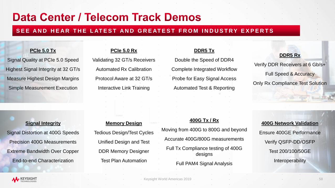
Please stop by the demo booth
Keysight World
58
S E E A N D H E A R T H E L AT E S T A N D G R E AT E S T F R O M I N D U S T R Y E X P E R T S
Keysight World Americas 2019
PCIe 5.0 Tx
Signal Quality at PCIe 5.0 Speed
Highest Signal Integrity at 32 GT/s
Measure Highest Design Margins
Simple Measurement Execution
Signal Integrity
Signal Distortion at 400G Speeds
Precision 400G Measurements
Extreme Bandwidth Over Copper
End-to-end Characterization
400G Network Validation
Ensure 400GE Performance
Verify QSFP-DD/OSFP
Test 200/100/50GE
Interoperability
PCIe 5.0 Rx
Validating 32 GT/s Receivers
Automated Rx Calibration
Protocol Aware at 32 GT/s
Interactive Link Training
DDR5 Tx
Double the Speed of DDR4
Complete Integrated Workflow
Probe for Easy Signal Access
Automated Test & Reporting
Memory Design
Tedious Design/Test Cycles
Unified Design and Test
DDR Memory Designer
Test Plan Automation
400G Tx / Rx
Moving from 400G to 800G and beyond
Accurate 400G/800G measurements
Full Tx Compliance testing of 400G
designs
Full PAM4 Signal Analysis
DDR5 Rx
Verify DDR Receivers at 6 Gb/s+
Full Speed & Accuracy
Only Rx Compliance Test Solution


60
c2c = Chip-to-Chip
c2m = Chip-to-Module
BER = Bit Error Ratio
BUJ = Bounded Uncorrelated Jitter (used to emulate crosstalk)
DUT = Device Under Test
EW = Eye Width
EH = Eye Height
FEC = Forward Error Correction
FFE = Feed-Forward Equalizer
NRZ = Non-Return to Zero (Refers to 2 level signaling or PAM-2)
PAM-n = Pulse Amplitude Modulation, where n = number of levels
RJ = Random Jitter
RS = Reed Solomon
SER = Symbol Error Ratio
SIRC – System Impulse Response Correction
SJ = Sinusoidal Jitter
SMF/MM F– Single-mode fiber, Multimode fiber
TDP = Transmitter and Dispersion Penalty
TDEC = Transmitter and Dispersion Eye Closure
TDECQ = Transmitter and dispersion eye closure quaternary (for PAM4)
Keysight World