433/868/915mhz rf transceiver with microcontroller and 4 ... · pdf fileembedded 8051...
TRANSCRIPT
PRODUCT SPECIFICATION
Main office: Nordic Semiconductor ASA - Vestre Rosten 81, N-7075 Tiller, Norway -Phone +4772898900 - Fax +4772898989Revision: 1.1 Page 1 of 104 June 2004
nRF9E5433/868/915MHz RF Transceiver withEmbedded 8051 CompatibleMicrocontroller and 4 Input, 10 Bit ADC
FEATURES• nRF905 433/868/915 MHz transceiver• 8051 compatible microcontroller
APPLICATIONS• Sports and leisure
equipment• 4 input, 10bit 80ksps ADC• Single 1.9V to 3.6V supply
• Alarm and securitysystem
• Small 32 pin QFN (5x5 mm) package • Industrial sensors• Extremely low cost Bill of Material (BOM) • Remote control• Internal VDD monitoring • Surveillance• 2.5µA standby with wakeup on timer or external pin • Automotive• Adjustable output power up to 10dBm • Telemetry• Channel switching time less than 650µs • Keyless entry• Low TX supply current, typical 11mA @-10dBm • Toys• Low RX supply current typical 12.5mA peak• Low MCU supply current, typ. 1mA at 4MHz @3volt• Suitable for frequency hopping• Carrier Detect for “listen before transmit protocol”
GENERAL DESCRIPTIONnRF9E5 is a true single chip system with fully integrated RF transceiver, 8051compatible microcontroller and a 4 input 10bit 80ksps AD converter. The transceiver ofthe system supports all the features available in the nRF905 chip includingShockburstTM, which automatically handles preamble, address and CRC. The circuit hasembedded voltage regulators, which provides maximum noise immunity and allowsoperation on a single 1.9V to 3.6V supply. nRF9E5 is compatible with FCC standardCFR47 part 15 and ETSI EN 300 220-1.
QUICK REFERENCE DATAParameter Value Unit
Minimum supply voltage 1.9 VTemperature range -40 to +85 °CSupply current in transmit @ -10dBm output power 11 mASupply current in receive mode 12.5 mASupply current for µ-controller 4MHz @ 3volt 1 mASupply current for ADC 0.9 mAMaximum transmit output power 10 dBmTransmitted data rate (Manchester-encoder embedded) 100 kbpsSensitivity -100 dBmSupply current in power down mode 2.5 µΑ
Table 1 nRF9E5 quick reference data.
PRODUCT SPECIFICATION
nRF9E5 Single Chip Transceiver with Embedded Microcontroller and ADC
Main office: Nordic Semiconductor ASA - Vestre Rosten 81, N-7075 Tiller, Norway -Phone +4772898900 - Fax +4772898989Revision: 1.1 Page 2 of 104 June 2004
ORDERING INFORMATION
Type number Description VersionnRF9E5 IC 32L QFN 5x5 mm -
nRF9E5-EVKIT 433 Evaluation kit 433MHz 1.0nRF9E5-EVKIT 868/915 Evaluation kit 868/915MHz 1.0
Table 2 nRF9E5 ordering information.
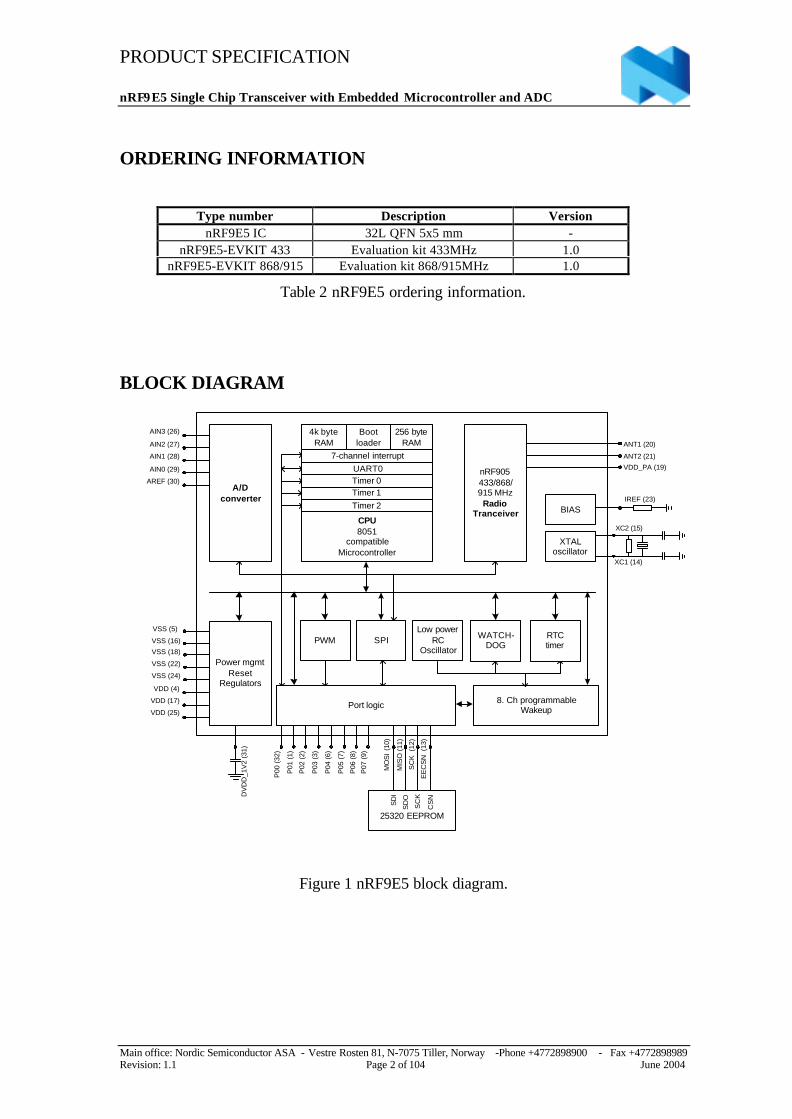
BLOCK DIAGRAM
VDD_PA (19)AIN0 (29)
AIN1 (28)
AIN2 (27)
AIN3 (26)
AREF (30)
IREF (23)
A/Dconverter
CPU8051
compatibleMicrocontroller
Timer 2Timer 1Timer 0UART0
7-channel interrupt
4k byteRAM
Bootloader
256 byteRAM
nRF905433/868/915 MHz
RadioTranceiver
XTALoscillator
BIAS
RTCtimer
WATCH-DOGSPIPWM
Low powerRC
Oscillator
Port logic
Power mgmtReset
Regulators
MIS
O (
11)
MO
SI
(10)
SC
K (
12)
EE
CS
N (
13)
XC1 (14)
XC2 (15)
VDD (4)
VDD (17)
VDD (25)
VSS (16)
VSS (18)
VSS (22)
VSS (24)
DV
DD
_1V
2 (3
1)
VSS (5)
P00
(32
)
P01
(1)
P02
(2)
P03
(3)
P04
(6)
P05
(7)
P06
(8)
P07
(9)
ANT2 (21)
ANT1 (20)
25320 EEPROM
SD
O
SD
I
CS
N
SC
K
8. Ch programmableWakeup
Figure 1 nRF9E5 block diagram.
PRODUCT SPECIFICATION
nRF9E5 Single Chip Transceiver with Embedded Microcontroller and ADC
Main office: Nordic Semiconductor ASA - Vestre Rosten 81, N-7075 Tiller, Norway -Phone +4772898900 - Fax +4772898989Revision: 1.1 Page 3 of 104 June 2004
TABLE OF CONTENTS1 Architectural Overview................................................................................................. 5
1.1 Microcontroller......................................................................................................... 51.2 PWM....................................................................................................................... 61.3 SPI.......................................................................................................................... 61.4 Port Logic ................................................................................................................ 61.5 Power Management .................................................................................................. 71.6 LF Clock, RTC Wakeup Timer, GPIO Wakeup and Watchdog .................................... 71.7 XTAL Oscillator....................................................................................................... 71.8 AD Converter .......................................................................................................... 81.9 Radio Transceiver..................................................................................................... 8
2 Eletrical Specification................................................................................................... 92.1 Detailed Current Information................................................................................... 10
3 Pin Assignment........................................................................................................... 114 Pin Function ............................................................................................................... 125 System Clock ............................................................................................................. 136 Digital I/O Ports......................................................................................................... 14
6.1 I/O Port Behavior During RESET............................................................................ 146.2 Port 0 (P0) ............................................................................................................. 146.3 Port 1 (P1 or SPI port) ............................................................................................ 15
7 Analog Interface......................................................................................................... 177.1 Crystal Specification ............................................................................................... 177.2 Antenna Output ...................................................................................................... 177.3 ADC Inputs............................................................................................................ 177.4 Current Reference .................................................................................................. 177.5 Digital Power De-Coupling ..................................................................................... 18
8 Internal Interface AD Converter and Transceiver.......................................................... 198.1 P2 - Radio General Purpose IO Port......................................................................... 19
9 Tranceiver Subsystem (nRF905) .................................................................................. 219.1 RF Modes of Operation........................................................................................... 219.2 nRF ShockBurst™ Mode ........................................................................................ 219.3 Standby Mode ........................................................................................................ 269.4 Output Power Adjustment ....................................................................................... 269.5 Modulation............................................................................................................. 269.6 Output Frequency................................................................................................... 279.7 Carrier Detect......................................................................................................... 279.8 Address Match....................................................................................................... 289.9 Data Ready ............................................................................................................ 289.10 Auto Retransmit ................................................................................................. 289.11 RX Reduced Power Mode................................................................................... 28
10 AD Converter subsystem ............................................................................................ 2910.1 AD Converter .................................................................................................... 2910.2 AD Converter Usage .......................................................................................... 3010.3 AD Converter Sampling and Timing .................................................................... 31
11 Tranceiver and AD Converter Configuration ................................................................ 3311.1 Internal SPI Register Configuration...................................................................... 3311.2 SPI – Instruction Set........................................................................................... 3511.3 SPI Timing......................................................................................................... 3611.4 RF Configuration – Register Description.............................................................. 3711.5 ADC - Configuration Register Description ........................................................... 3811.6 Status-Register Description ................................................................................. 3811.7 RF - Register Contents........................................................................................ 39
PRODUCT SPECIFICATION
nRF9E5 Single Chip Transceiver with Embedded Microcontroller and ADC
Main office: Nordic Semiconductor ASA - Vestre Rosten 81, N-7075 Tiller, Norway -Phone +4772898900 - Fax +4772898989Revision: 1.1 Page 4 of 104 June 2004
11.8 ADC Configuration Register Contents ................................................................. 4011.9 ADC Data Register Contents............................................................................... 4011.10 Status Register Contents ..................................................................................... 40
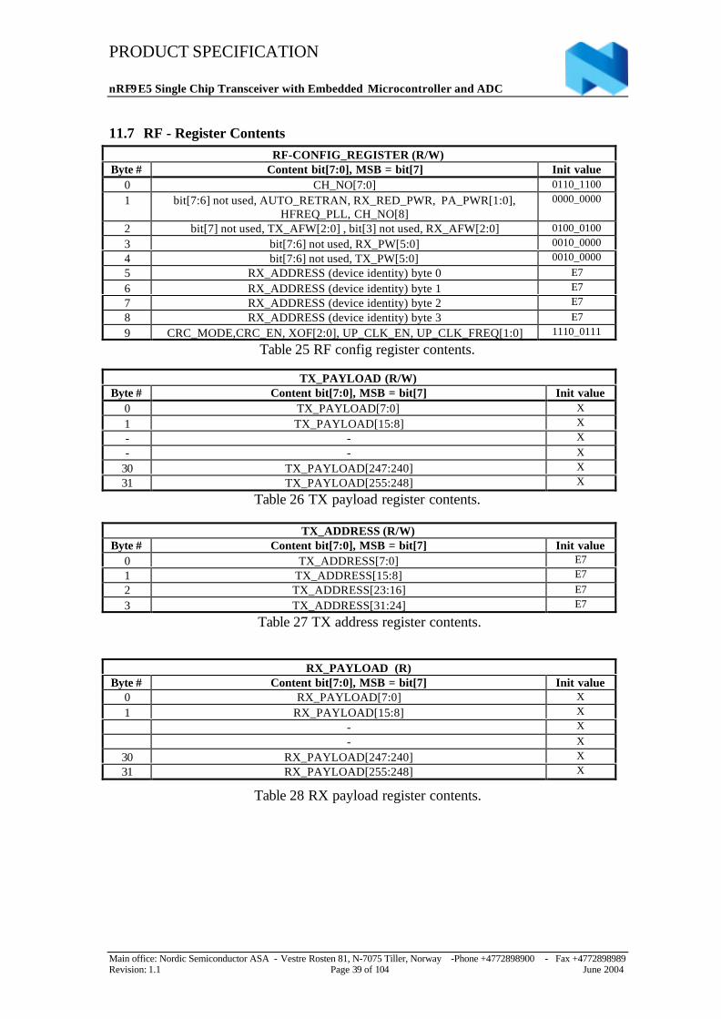
12 Tranceiver Subsytem Timing....................................................................................... 4112.1 Device Switching Times ..................................................................................... 4112.2 ShockBurstTM TX Timing.................................................................................... 4112.3 ShockBurstTM RX Timing.................................................................................... 42
13 SPI............................................................................................................................ 4314 PWM......................................................................................................................... 4415 Interrupts ................................................................................................................... 45
15.1 Interrupt SFRs.................................................................................................... 4515.2 Interrupt Processing ............................................................................................ 4815.3 Interrupt Masking ............................................................................................... 4815.4 Interrupt Priorities .............................................................................................. 4815.5 Interrupt Sampling .............................................................................................. 4915.6 Interrupt Latency................................................................................................ 5015.7 Interrupt Latency from Power Down State. .......................................................... 5015.8 Single-Step Operation ......................................................................................... 50
16 LF Clock Wakeup Functions and Watchdog ................................................................. 5116.1 The LF Clock..................................................................................................... 5116.2 Tick Calibration.................................................................................................. 5116.3 RTC Wakeup Timer............................................................................................ 5216.4 Programmable GPIO Wakeup Function................................................................ 5216.5 Watchdog........................................................................................................... 5316.6 Programming Interface to Watchdog and Wakeup Functions ................................. 5316.7 Reset................................................................................................................. 55
17 Power Saving Modes .................................................................................................. 5717.1 Standard 8051 Power Saving Modes .................................................................... 5717.2 Additional Power Down Modes........................................................................... 58
18 Microcontroller........................................................................................................... 6018.1 Memory Organization......................................................................................... 6018.2 Program Format in External EEPROM................................................................ 6118.3 Instruction Set.................................................................................................... 6218.4 Instruction Timing .............................................................................................. 6818.5 Dual Data Pointers.............................................................................................. 6818.6 Special Function Registers .................................................................................. 6918.7 SFR Registers Unique to nRF9E5........................................................................ 7318.8 Timers/Counters................................................................................................. 7418.9 Serial Interface................................................................................................... 81
19 Package Outline.......................................................................................................... 9220 PCB Layout and Decoupling Guidelines ...................................................................... 9321 Application Examples................................................................................................. 94
21.1 Differential Connection to a Loop Antenna .......................................................... 9421.2 PCB Layout Example, Differential Connection to a Loop Antenna ........................ 9621.3 Single Ended Connection to 50Ω Antenna............................................................ 9721.4 PCB Layout Example, Single Ended Connection to 50Ω Antenna ......................... 9921.5 Configure the Chip as nRF905. ............................................................................ 99
22 Absolute Maximum Ratings .......................................................................................10023 Glossery of Terms .....................................................................................................10124 Definitions ................................................................................................................10225 Your Notes ...............................................................................................................103
PRODUCT SPECIFICATION
nRF9E5 Single Chip Transceiver with Embedded Microcontroller and ADC
Main office: Nordic Semiconductor ASA - Vestre Rosten 81, N-7075 Tiller, Norway -Phone +4772898900 - Fax +4772898989Revision: 1.1 Page 5 of 104 June 2004
1 ARCHITECTURAL OVERVIEW
This section will give a brief overview of each of the blocks in the block diagram inFigure 1.
1.1 MicrocontrollerThe nRF9E5 microcontroller is instruction set compatible with the industry standard8051. Instruction timing is slightly different from the industry standard, typically eachinstruction will use from 4 to 20 clock cycles, compared with 12 to 48 for the“standard”. The interrupt controller is extended to support 5 additional interrupt sources;ADC, SPI, 2 for the radio and a wakeup function. There are also 3 timers that are 8052compatible, plus some extensions, in the microcontroller core. An 8051 compatibleUART that can use timer1 or timer2 for baud rate generation in the traditionalasynchronous modes is included. The CPU is equipped with 2 data pointers to facilitateeasier moving of data in the XRAM area, which is a common 8051 extension. Themicrocontroller clock is derived from the crystal oscillator.
1.1.1 Memory ConfigurationThe microcontroller has a 256-byte data ram (8052 compatible, with the upper half onlyaddressable by register indirect addressing). A small ROM of 512 bytes contains abootstrap loader that is executed automatically after power on reset or if initiated bysoftware later. The user program is normally loaded into a 4k byte RAM1 from anexternal serial EEPROM by the bootstrap loader. The 4k byte RAM may also (partially)be used for data storage in some applications.
1.1.2 Boot EEPROM/FLASHThe program code for the device must be loaded from an external non-volatile memory.The default boot loader expects this to be a “generic 25320” EEPROM with SPIinterface. These memories are available from several vendors with supply ranges downto 1.8V. The SPI interface uses the pins MISO (from EEPROM SDO), SCK (toEEPROM SCK), MOSI (to EEPROM SDI) and EECSN (to EEPROM CSN). When theboot is completed, the MISO (P1.2), MOSI (P1.0) and SCK (P1.1) pins may be used forother purposes such as other SPI devices or GPIO (General Purpose Input Output).
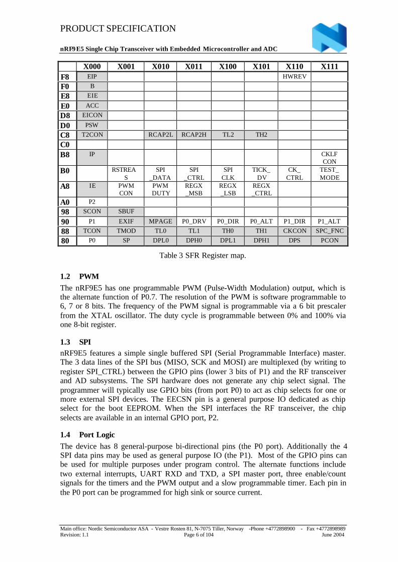
1.1.3 Register MapThe SFR (Special Function Registers) control several of the features of the nRF9E5.Most of the nRF9E5 SFRs are identical to the standard 8051 SFRs. However, there areadditional SFRs that control features that are not available in the standard 8051.The SFR map is shown in Table 3. The registers with grey background are registers withindustry standard 8051 behavior. Note that the function of P0, P1 and P2 are somewhatdifferent from the “standard” even if the conventional addresses (0x80, 0x90 and 0xA0)are used.
1 Optionally this 4k block of memory can be configured as 2k mask ROM and 2k RAM or 4 k mask ROM
PRODUCT SPECIFICATION
nRF9E5 Single Chip Transceiver with Embedded Microcontroller and ADC
Main office: Nordic Semiconductor ASA - Vestre Rosten 81, N-7075 Tiller, Norway -Phone +4772898900 - Fax +4772898989Revision: 1.1 Page 6 of 104 June 2004
X000 X001 X010 X011 X100 X101 X110 X111F8 EIP HWREV
F0 B
E8 EIE
E0 ACC
D8 EICON
D0 PSW
C8 T2CON RCAP2L RCAP2H TL2 TH2
C0B8 IP CKLF
CONB0 RSTREA
SSPI
_DATASPI
_CTRLSPI
CLKTICK_
DVCK_
CTRLTEST_MODE
A8 IE PWMCON
PWMDUTY
REGX_MSB
REGX_LSB
REGX_CTRL
A0 P2
98 SCON SBUF
90 P1 EXIF MPAGE P0_DRV P0_DIR P0_ALT P1_DIR P1_ALT
88 TCON TMOD TL0 TL1 TH0 TH1 CKCON SPC_FNC
80 P0 SP DPL0 DPH0 DPL1 DPH1 DPS PCON
Table 3 SFR Register map.
1.2 PWMThe nRF9E5 has one programmable PWM (Pulse-Width Modulation) output, which isthe alternate function of P0.7. The resolution of the PWM is software programmable to6, 7 or 8 bits. The frequency of the PWM signal is programmable via a 6 bit prescalerfrom the XTAL oscillator. The duty cycle is programmable between 0% and 100% viaone 8-bit register.
1.3 SPInRF9E5 features a simple single buffered SPI (Serial Programmable Interface) master.The 3 data lines of the SPI bus (MISO, SCK and MOSI) are multiplexed (by writing toregister SPI_CTRL) between the GPIO pins (lower 3 bits of P1) and the RF transceiverand AD subsystems. The SPI hardware does not generate any chip select signal. Theprogrammer will typically use GPIO bits (from port P0) to act as chip selects for one ormore external SPI devices. The EECSN pin is a general purpose IO dedicated as chipselect for the boot EEPROM. When the SPI interfaces the RF transceiver, the chipselects are available in an internal GPIO port, P2.
1.4 Port LogicThe device has 8 general-purpose bi-directional pins (the P0 port). Additionally the 4SPI data pins may be used as general purpose IO (the P1). Most of the GPIO pins canbe used for multiple purposes under program control. The alternate functions includetwo external interrupts, UART RXD and TXD, a SPI master port, three enable/countsignals for the timers and the PWM output and a slow programmable timer. Each pin inthe P0 port can be programmed for high sink or source current.
PRODUCT SPECIFICATION
nRF9E5 Single Chip Transceiver with Embedded Microcontroller and ADC
Main office: Nordic Semiconductor ASA - Vestre Rosten 81, N-7075 Tiller, Norway -Phone +4772898900 - Fax +4772898989Revision: 1.1 Page 7 of 104 June 2004
1.5 Power ManagementThe nRF9E5 can be placed into several low power modes under program control, andalso the ADC and RF subsystems can be turned on or off under program control. TheCPU will stop, but all RAM’s and registers maintain their values. The watchdog, RTC(Real Time Clock) wakeup timer and the GPIO wakeup function are always activeduring power down. The current consumption is typically 2.5µA when running with thecrystal oscillator off.The device can exit the power down modes by an external pin, an event on any of the P0GPIO pins, by the wakeup timer if enabled or by a watchdog reset.
1.6 LF Clock, RTC Wakeup Timer, GPIO Wakeup and WatchdogThe nRF9E5 contains an internal low frequency clock CKLF that is always on. Whenthe crystal oscillator clocks the circuit, the CKLF is a 4kHz clock derived from thecrystal oscillator. When no crystal oscillator clock is available, the CKLF is a low powerRC oscillator that cannot be disabled, so it will run continuously as long as VDD =1.8V. The RTC Wakeup timer, the GPIO wakeup and watchdog all run on the CKLF toensure these vital functions will work during all power down modes.
RTC Wakeup timer is a 24 bit programmable down counter and the Watchdog is a 16 bitprogrammable down counter. The resolution of the watchdog and wakeup timer isprogrammable (with prescaler TICK_DV) from approximately 300µs to approximately80ms. By default the resolution is 1ms. The wakeup timer can be started and stopped byuser software. The watchdog is disabled after a reset, but if activated it cannot bedisabled again, except by another reset. An RTC Wakeup timer timeout also provides aprogrammable pulse (GTIMER) that can be an output on a GPIO pin.
The GPIO wakeup function lets the software enable wakeup on one or more pins fromthe P0 GPIO port. The edge sensitivity (rising, falling or both) and de-bouncing filter isindividually programmable for each pin.
1.7 XTAL OscillatorThe microcontroller, AD converter and transceiver run on the same crystal oscillatorgenerated clock. A range of crystals frequencies from 4 to 20 MHz may be utilized. Fordetails, please see chapter 7.1 on page 17. The oscillator may be started and stopped asrequested by software.
PRODUCT SPECIFICATION
nRF9E5 Single Chip Transceiver with Embedded Microcontroller and ADC
Main office: Nordic Semiconductor ASA - Vestre Rosten 81, N-7075 Tiller, Norway -Phone +4772898900 - Fax +4772898989Revision: 1.1 Page 8 of 104 June 2004
1.8 AD ConverterThe nRF9E5 AD converter has up to 10-bit dynamic range and linearity with aconversion rate of 80 ksps used at the Nyquist rate. The reference for the AD converteris software selectable between the AREF input and an internal 1.22V bandgap reference.The converter has 5 inputs selectable by software. Selecting one of the inputs 0 to 3 willconvert the voltage on the respective AIN0 to AIN3 pin. Input 4 enables software tomonitor the nRF9E5 supply voltage by converting an internal input that is VDD/3 withthe 1.22V internal reference selected. The AD converter is typically used in a start/stopmode. The sampling time is then under software control. The converter is by defaultconfigured as 10 bits. For special requirements, the AD converter can be configured bysoftware to perform 6, 8 or 12 bit conversions. The converter may also be used indifferential mode with AIN0 used as negative input and one of the other 3 externalinputs used as noninverting input.
1.9 Radio TransceiverThe transceiver part of the circuit has identical functionality to the nRF905 single chipRF transceiver. It is accessed through an internal parallel port and / or an internal SPI.The data ready, carrier-detect and address match signals can be programmed asinterrupts to the microcontroller or polled via a GPIO port.The nRF905 is a radio transceiver for the 433/868/915 MHz ISM bands. The transceiverconsists of a fully integrated frequency synthesizer, a power amplifier, a modulator anda receiver unit. Output power and frequency channels and other RF parameters are easilyprogrammable by use of the on chip SPI interface to the nRF905 core. RF currentconsumption is only 11 mA in TX mode (output power -10dBm) and 12.5 mA in RXmode. For power saving the transceiver can be turned on / off under software control.This document should be read in conjunction with the nRF905 datasheet.
PRODUCT SPECIFICATION
nRF9E5 Single Chip Transceiver with Embedded Microcontroller and ADC
Main office: Nordic Semiconductor ASA - Vestre Rosten 81, N-7075 Tiller, Norway -Phone +4772898900 - Fax +4772898989Revision: 1.1 Page 9 of 104 June 2004
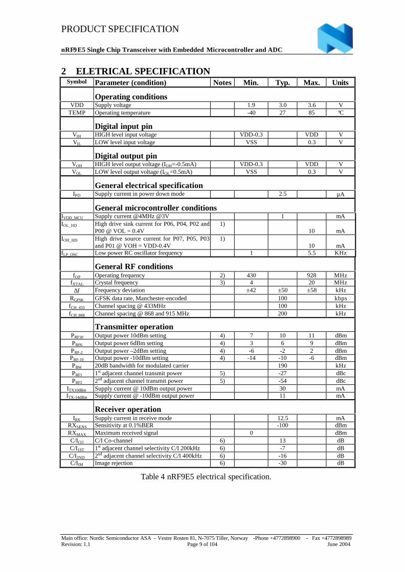
2 ELETRICAL SPECIFICATIONSymbol Parameter (condition) Notes Min. Typ. Max. Units
Operating conditionsVDD Supply voltage 1.9 3.0 3.6 V
TEMP Operating temperature -40 27 85 ºC
Digital input pinVIH HIGH level input voltage VDD-0.3 VDD VVIL LOW level input voltage VSS 0.3 V
Digital output pinVOH HIGH level output voltage (IOH=-0.5mA) VDD-0.3 VDD VVOL LOW level output voltage (IOL=0.5mA) VSS 0.3 V
General electrical specificationIPD Supply current in power down mode 2.5 µA
General microcontroller conditionsIVDD_MCU Supply current @4MHz @3V 1 mAIOL_HD High drive sink current for P06, P04, P02 and
P00 @ VOL = 0.4V1)
10 mAIOH_HD High drive source current for P07, P05, P03
and P01 @ VOH = VDD-0.4V1)
10 mAfLP_OSC Low power RC oscillator frequency 1 5.5 KHz
General RF conditionsfOP Operating frequency 2) 430 928 MHz
fXTAL Crystal frequency 3) 4 20 MHz∆f Frequency deviation ±42 ±50 ±58 kHz
RGFSK GFSK data rate, Manchester-encoded 100 kbpsfCH_433 Channel spacing @ 433MHz 100 kHzfCH_868 Channel spacing @ 868 and 915 MHz 200 kHz
Transmitter operationPRF10 Output power 10dBm setting 4) 7 10 11 dBmPRF6 Output power 6dBm setting 4) 3 6 9 dBmPRF-2 Output power –2dBm setting 4) -6 -2 2 dBmPRF-10 Output power -10dBm setting 4) -14 -10 -6 dBmPBW 20dB bandwidth for modulated carrier 190 kHzPRF1 1st adjacent channel transmit power 5) -27 dBcPRF2 2nd adjacent channel transmit power 5) -54 dBc
ITX10dBm Supply current @ 10dBm output power 30 mAITX-14dBm Supply current @ -10dBm output power 11 mA
Receiver operationIRX Supply current in receive mode 12.5 mA
RXSENS Sensitivity at 0.1%BER -100 dBmRXMAX Maximum received signal 0 dBmC/ICO C/I Co-channel 6) 13 dBC/I1ST 1st adjacent channel selectivity C/I 200kHz 6) -7 dBC/I2ND 2nd adjacent channel selectivity C/I 400kHz 6) -16 dBC/IIM Image rejection 6) -30 dB
Table 4 nRF9E5 electrical specification.

PRODUCT SPECIFICATION
nRF9E5 Single Chip Transceiver with Embedded Microcontroller and ADC
Main office: Nordic Semiconductor ASA - Vestre Rosten 81, N-7075 Tiller, Norway -Phone +4772898900 - Fax +4772898989Revision: 1.1 Page 10 of 104 June 2004
Symbol Parameter (condition) Notes Min. Typ. Max. Units
ADC operationDNL Differential Nonlinearity fIN = 0.9991 kHz ±0.5 LSBINL Integral Nonlinearity fIN = 0.9991 kHz ±0.75 LSBSNR Signal to Noise Ratio (DC input) 59 dBFSVOS Midscale offset ± 1 %FSεG Gain Error ±1 %FSSNR Signal to Noise Ratio (without harmonics)
fIN = 10 kHz53 58 dBFS
SFDR Spurious Free Dynamic Range fIN = 10 kHz 65 dBVBG Internal reference 1.1 1.22 1.3 V
Internal reference voltage drift 100 ppm/°CVFS Reference voltage input (external ref) 0.8 1.5 VFS Conversion rate 7) 125 ksps
IADC Supply current ADC operation 1 mAtNPD Start-up time from ADC Power down 15 µs
Table 5 nRF9E5 AD converter electrical specifications.
1) Higher sink/source current is possible if increased voltage changes on ports are accepted.2) Operates in the 433, 868 and 915 MHz ISM band.3) The crystal frequency may be chosen from 5 different values (4, 8, 12, 16, and 20MHz) which are specified in
the configuration word. Please see Table 22 on page 37.4) Optimum Load Impedance.5) Channel width and channel spacing is 200kHz.6) Channel Level +3dB over sensitivity, interfering signal a standard carrier wave, Image 2 MHz above wanted.7) Conversion rate is dependant on resolution, Please see chapter 10.3 page 31.
2.1 Detailed Current Information
MODE TYPICAL CURRENTLight power down 0.4 mAModerate Power down 125 uAStandby mode 25 uADeep Power Down 2.5 uAMCU @0.5M 3 volt 0.125 mAMCU @1M 3 volt 0.25 mAMCU @2M 3 volt 0.5 mAMCU @4M 3 volt 1 mAMCU @8M 3 volt 2 mAMCU @12M 3 volt 3 mAMCU @16M 3 volt 4 mAMCU @20M 3 volt 5 mARx @ 433 12.2 mARx @ 868/915 12.8 mAReduced Rx 10.5 mATx @ 10dBm 30 mATx @ 6dBm 20 mATx @ -2dBm 14 mATx @ -10dBm 11 mA
Table 6 Detailed current information
PRODUCT SPECIFICATION
nRF9E5 Single Chip Transceiver with Embedded Microcontroller and ADC
Main office: Nordic Semiconductor ASA - Vestre Rosten 81, N-7075 Tiller, Norway -Phone +4772898900 - Fax +4772898989Revision: 1.1 Page 11 of 104 June 2004
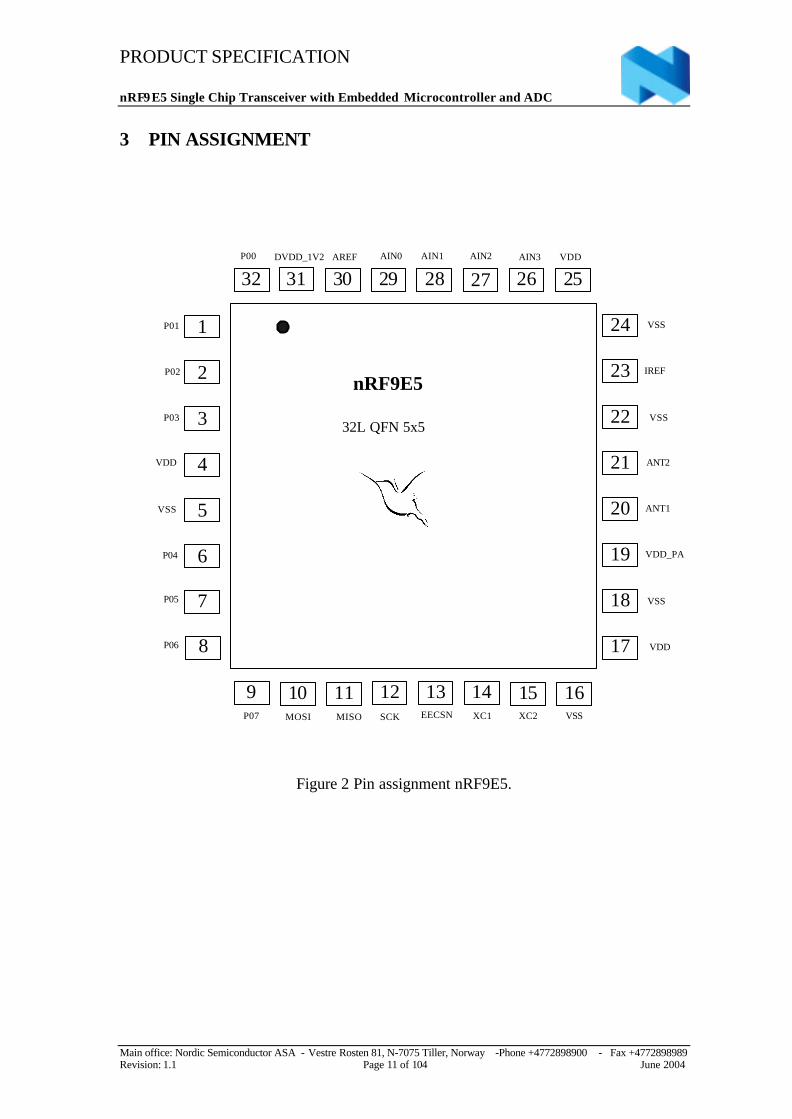
3 PIN ASSIGNMENT
nRF9E5
32L QFN 5x5
MISO
VSS
P04
DVDD_1V2
P05
XC2 VSS
P06
P07
ANT2
VDD_PA
VSS
ANT1
VSS
AIN0 VDD
VSS
P01
XC1
4
3
2
1
6
5
7
8
9 13 1412 1510 11 16
24
23
22
20
19
21
18
17
29 28 2730 26 253132
VDD
AREFP00
IREF
AIN1 AIN2 AIN3
MOSI
P02
P03
VDD
EECSNSCK
Figure 2 Pin assignment nRF9E5.
PRODUCT SPECIFICATION
nRF9E5 Single Chip Transceiver with Embedded Microcontroller and ADC
Main office: Nordic Semiconductor ASA - Vestre Rosten 81, N-7075 Tiller, Norway -Phone +4772898900 - Fax +4772898989Revision: 1.1 Page 12 of 104 June 2004
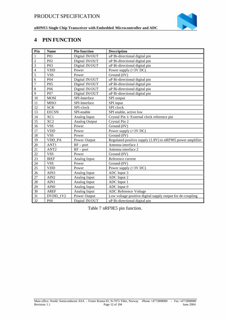
4 PIN FUNCTION
Pin Name Pin function Description1 P01 Digital IN/OUT uP Bi-directional digital pin2 P02 Digital IN/OUT uP Bi-directional digital pin3 P03 Digital IN/OUT uP Bi-directional digital pin4 VDD Power Power supply (+3V DC)5 VSS Power Ground (0V)6 P04 Digital IN/OUT uP Bi-directional digital pin7 P05 Digital IN/OUT uP Bi-directional digital pin8 P06 Digital IN/OUT uP Bi-directional digital pin9 P07 Digital IN/OUT uP Bi-directional digital pin10 MOSI SPI-Interface SPI output11 MISO SPI-Interface SPI input12 SCK SPI-clock SPI clock13 EECSN SPI-enable SPI enable, active low14 XC1 Analog Input Crystal Pin 1/ External clock reference pin15 XC2 Analog Output Crystal Pin 216 VSS Power Ground (0V)17 VDD Power Power supply (+3V DC)18 VSS Power Ground (0V)19 VDD_PA Power Output Regulated positive supply (1.8V) to nRF905 power amplifier20 ANT1 RF – port Antenna interface 121 ANT2 RF – port Antenna interface 222 VSS Power Ground (0V)23 IREF Analog Input Reference current24 VSS Power Ground (0V)25 VDD Power Power supply (+3V DC)26 AIN3 Analog Input ADC Input 327 AIN2 Analog Input ADC Input 228 AIN1 Analog Input ADC Input 129 AIN0 Analog Input ADC Input 030 AREF Analog Input ADC Reference Voltage31 DVDD_1V2 Power Output Low voltage positive digital supply output for de-coupling32 P00 Digital IN/OUT uP Bi-directional digital pin
Table 7 nRF9E5 pin function.
PRODUCT SPECIFICATION
nRF9E5 Single Chip Transceiver with Embedded Microcontroller and ADC
Main office: Nordic Semiconductor ASA - Vestre Rosten 81, N-7075 Tiller, Norway -Phone +4772898900 - Fax +4772898989Revision: 1.1 Page 13 of 104 June 2004
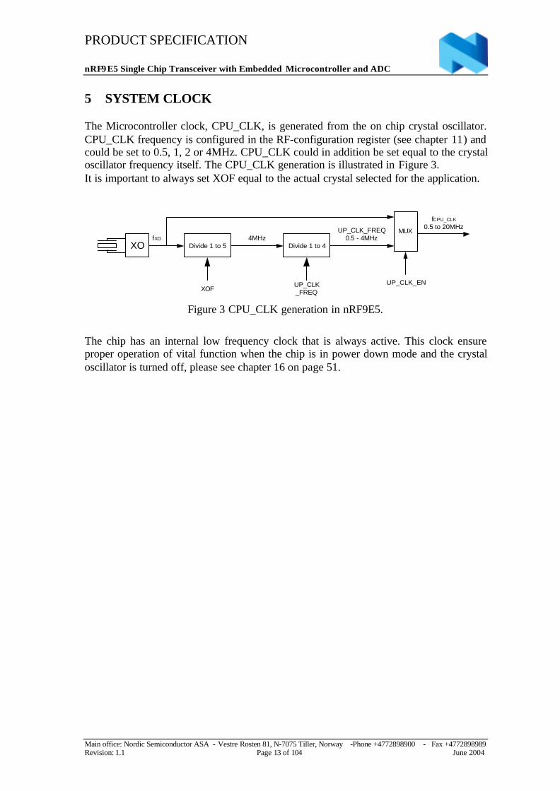
5 SYSTEM CLOCK
The Microcontroller clock, CPU_CLK, is generated from the on chip crystal oscillator.CPU_CLK frequency is configured in the RF-configuration register (see chapter 11) andcould be set to 0.5, 1, 2 or 4MHz. CPU_CLK could in addition be set equal to the crystaloscillator frequency itself. The CPU_CLK generation is illustrated in Figure 3.It is important to always set XOF equal to the actual crystal selected for the application.
XOfXO
Divide 1 to 5 Divide 1 to 44MHz
UP_CLK_FREQ0.5 - 4MHz
MUX
fCPU_CLK
0.5 to 20MHz
XOFUP_CLK_FREQ
UP_CLK_EN
Figure 3 CPU_CLK generation in nRF9E5.
The chip has an internal low frequency clock that is always active. This clock ensureproper operation of vital function when the chip is in power down mode and the crystaloscillator is turned off, please see chapter 16 on page 51.
PRODUCT SPECIFICATION
nRF9E5 Single Chip Transceiver with Embedded Microcontroller and ADC
Main office: Nordic Semiconductor ASA - Vestre Rosten 81, N-7075 Tiller, Norway -Phone +4772898900 - Fax +4772898989Revision: 1.1 Page 14 of 104 June 2004
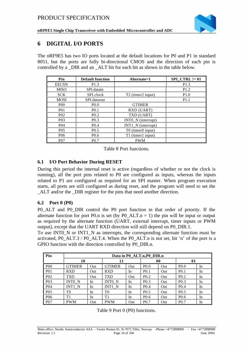
6 DIGITAL I/O PORTS
The nRF9E5 has two IO ports located at the default locations for P0 and P1 in standard8051, but the ports are fully bi-directional CMOS and the direction of each pin iscontrolled by a _DIR and an _ALT bit for each bit as shown in the table below.
Pin Default function Alternate=1 SPI_CTRL != 01EECSN P1.3 P1.3MISO SPI.datain P1.2SCK SPI.clock T2 (timer2 input) P1.0MOSI SPI.dataout P1.1P00 P0.0 GTIMERP01 P0.1 RXD (UART)P02 P0.2 TXD (UART)P03 P0.3 INT0_N (interrupt)P04 P0.4 INT1_N (interrupt)P05 P0.5 T0 (timer0 input)P06 P0.6 T1 (timer1 input)P07 P0.7 PWM
Table 8 Port functions.
6.1 I/O Port Behavior During RESETDuring this period the internal reset is active (regardless of whether or not the clock isrunning), all the port pins related to P0 are configured as inputs, whereas the inputsrelated to P1 are configured as required for an SPI master. When program executionstarts, all ports are still configured as during reset, and the program will need to set the_ALT and/or the _DIR register for the pins that need another direction.
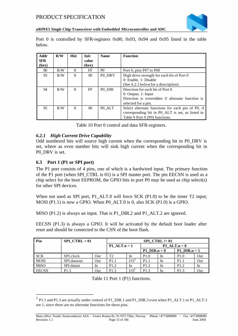
6.2 Port 0 (P0)P0_ALT and P0_DIR control the P0 port function in that order of priority. If thealternate function for port P0.n is set (by P0_ALT.n = 1) the pin will be input or outputas required by the alternate function (UART, external interrupt, timer inputs or PWMoutput), except that the UART RXD direction will still depend on P0_DIR.1.To use INT0_N or INT1_N as interrupts, the corresponding alternate function must beactivated, P0_ALT.3 / P0_ALT.4. When the P0_ALT.n is not set, bit ‘n’ of the port is aGPIO function with the direction controlled by P0_DIR.n.
Data in P0_ALT.n,P0_DIR.nPin10 11 00 01
P00 GTIMER Out GTIMER Out P0.0 Out P0.0 InP01 RXD Out RXD In P0.1 Out P0.1 InP02 TXD Out TXD Out P0.2 Out P0.2 InP03 INT0_N In INT0_N In P0.3 Out P0.3 InP04 INT1_N In INT1_N In P0.4 Out P0.4 InP05 T0 In T0 In P0.5 Out P0.5 InP06 T1 In T1 In P0.6 Out P0.6 InP07 PWM Out PWM Out P0.7 Out P0.7 In
Table 9 Port 0 (P0) functions.
PRODUCT SPECIFICATION
nRF9E5 Single Chip Transceiver with Embedded Microcontroller and ADC
Main office: Nordic Semiconductor ASA - Vestre Rosten 81, N-7075 Tiller, Norway -Phone +4772898900 - Fax +4772898989Revision: 1.1 Page 15 of 104 June 2004
Port 0 is controlled by SFR-registers 0x80, 0x93, 0x94 and 0x95 listed in the tablebelow.
AddrSFR(hex)
R/W #bit Initvalue(hex)
Name Function
80 R/W 8 FF P0 Port 0, pins P07 to P0093 R/W 8 00 P0_DRV High drive strength for each bit of Port 0
0: Enable, 1: Disable(See 6.2.1 below for a description)
94 R/W 8 FF P0_DIR Direction for each bit of Port 00: Output, 1: InputDirection is overridden if alternate function isselected for a pin.
95 R/W 8 00 P0_ALT Select alternate functions for each pin of P0, ifcorresponding bit in P0_ALT is set, as listed inTable 9 Port 0 (P0) functions.
Table 10 Port 0 control and data SFR-registers.
6.2.1 High Current Drive CapabilityOdd numbered bits will source high current when the corresponding bit in P0_DRV isset, where as even number bits will sink high current when the corresponding bit inP0_DRV is set.
6.3 Port 1 (P1 or SPI port)The P1 port consists of 4 pins, one of which is a hardwired input. The primary functionof the P1 port (when SPI_CTRL is 01) is a SPI master port. The pin EECSN is used as achip select for the boot EEPROM, the GPIO bits in port P0 may be used as chip select(s)for other SPI devices.
When not used as SPI port, P1_ALT.0 will force SCK (P1.0) to be the timer T2 input;MOSI (P1.1) is now a GPIO. When P0_ALT.0 is 0, also SCK (P1.0) is a GPIO.
MISO (P1.2) is always an input. That is P1_DIR.2 and P1_ALT.2 are ignored.
EECSN (P1.3) is always a GPIO. It will be activated by the default boot loader afterreset and should be connected to the CSN of the boot flash.
SPI_CTRL != 01P1_ALT.n = 0
Pin SPI_CTRL = 01P1_ALT.n = 1
P1_DIR.n = 0 P1_DIR.n = 1SCK SPI.clock Out T2 In P1.0 In P1.0 OutMOSI SPI.dataout Out P1.1 I/O2 P1.1 In P1.1 OutMISO SPI.datain In P1.2 In P1.2 In P1.2 InEECSN P1.3 Out P1.3 I/O2 P1.3 In P1.3 Out
Table 11 Port 1 (P1) functions.
2 P1.1 and P1.3 are actually under control of P1_DIR.1 and P1_DIR.3 even when P1_ALT.1 or P1_ALT.3are 1, since there are no alternate functions for these pins.
PRODUCT SPECIFICATION
nRF9E5 Single Chip Transceiver with Embedded Microcontroller and ADC
Main office: Nordic Semiconductor ASA - Vestre Rosten 81, N-7075 Tiller, Norway -Phone +4772898900 - Fax +4772898989Revision: 1.1 Page 16 of 104 June 2004
Port 1 is controlled by SFR-registers 0x90, 0x96 and 0x97, and only the 4 lower bits ofthe registers are used.
AddrSFR(hex)
R/W #bit Initvalue(hex)
Name Function
90 R/W 4 F P1 Port 1, pins SPI_SCK, SPI_MOSI, SPI_MISO andSPI_CSN
96 R/W 4 4 P1_DIR Direction for each bit of Port 10: Output, 1: InputDirection is overridden if alternate function is selectedfor a pin, or if SPI_CTRL=01.SPI_MISO is always input.
97 R/W 4 0 P1_ALT Select alternate functions for each pin of P1if corresponding bit in P1_ALT is set, as listed in Table11 Port 1 (P1) functions
Table 12 Port 1 control and data SFR-registers.
P1 is by default configured as a SPI master port. In this case, it is then controlled by the3 SFR registers 0xB2, 0xB3 and 0xB4 as shown in Table 33 on page 43.
PRODUCT SPECIFICATION
nRF9E5 Single Chip Transceiver with Embedded Microcontroller and ADC
Main office: Nordic Semiconductor ASA - Vestre Rosten 81, N-7075 Tiller, Norway -Phone +4772898900 - Fax +4772898989Revision: 1.1 Page 17 of 104 June 2004
7 ANALOG INTERFACE
7.1 Crystal SpecificationTolerance includes initially accuracy and tolerance over temperature and aging.
Frequency CL ESR C0max Tolerance @868/915 MHz
Tolerance @433 MHz
4MHz 12pF 150Ω 7.0pF ±30ppm ±60ppm8MHz 12pF 100Ω 7.0pF ±30ppm ±60ppm
12MHz 12pF 100Ω 7.0pF ±30ppm ±60ppm16MHz 12pF 100Ω 7.0pF ±30ppm ±60ppm20MHz 12pF 100Ω 7.0pF ±30ppm ±60ppm
Table 13 Crystal specification of nRF9E5.
To achieve a crystal oscillator solution with low power consumption and fast start-uptime, it is recommended to specify the crystal with a low value of crystal loadcapacitance. Specifying CL =12pF is acceptable, but it is possible to use up to 16pF.Specifying a lower value of crystal parallel equivalent capacitance, Co=1.5pF is alsogood, but this can increase the price of the crystal itself. Typically Co=1.5pF at a crystalspecified for Co_max=7.0pF.
7.2 Antenna OutputThe “ANT1 & ANT2” output pins provide a balanced RF output to the antenna. Thepins must have a DC path to VDD_PA, either via a RF choke or via the center point in adipole antenna. The load impedance seen between the ANT1/ANT2 outputs should be inthe range 200-700Ω. The optimum differential load impedance at the antenna ports isgiven as:
900MHz 225Ω+j210430MHz 300Ω+j100
A low load impedance (for instance 50Ω) can be obtained by fitting a simple matchingnetwork or a RF transformer (balun). Further information regarding balun structures andmatching networks may be found in the Application Examples chapter.
7.3 ADC InputsThe Analog to digital converter has four analog input channels and one referencevoltage input. Analog input is selected with CHSEL in the ADC_CONFIG_REG.
7.4 Current ReferenceTo get accurate internal biasing, an external low tolerance resistor is used. A resistor of22kΩ and 1% accuracy should be connected between the pin IREF and ground forproper operation of nRF9E5.
PRODUCT SPECIFICATION
nRF9E5 Single Chip Transceiver with Embedded Microcontroller and ADC
Main office: Nordic Semiconductor ASA - Vestre Rosten 81, N-7075 Tiller, Norway -Phone +4772898900 - Fax +4772898989Revision: 1.1 Page 18 of 104 June 2004
7.5 Digital Power De-CouplingnRF9E5 has internal regulator used for optimum performance and minimum powerdissipation in digital part of the system. De-coupling of the regulated power is neededfor proper operation of the chip. A capacitor of 10nF should be connected betweenDVDD_1V2 and ground as close to the chip as possible. Please see PCB layout and de-coupling guidelines for further information regarding layout.
PRODUCT SPECIFICATION
nRF9E5 Single Chip Transceiver with Embedded Microcontroller and ADC
Main office: Nordic Semiconductor ASA - Vestre Rosten 81, N-7075 Tiller, Norway -Phone +4772898900 - Fax +4772898989Revision: 1.1 Page 19 of 104 June 2004
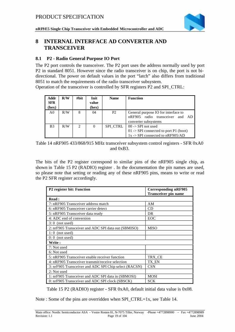
8 INTERNAL INTERFACE AD CONVERTER ANDTRANSCEIVER
8.1 P2 - Radio General Purpose IO PortThe P2 port controls the transceiver. The P2 port uses the address normally used by portP2 in standard 8051. However since the radio transceiver is on chip, the port is not bi-directional. The power on default values in the port “latch” also differs from traditional8051 to match the requirements of the radio transceiver subsystem.Operation of the transceiver is controlled by SFR registers P2 and SPI_CTRL:
AddrSFR(hex)
R/W #bit Initvalue(hex)
Name Function
A0 R/W 8 04 P2 General purpose IO for interface tonRF905 radio transceiver and ADconverter subsystems
B3 R/W 2 0 SPI_CTRL 00 -> SPI not used01 -> SPI connected to port P1 (boot)1x -> SPI connected to nRF905/AD
Table 14 nRF905 433/868/915 MHz transceiver subsystem control registers - SFR 0xA0and 0xB3.
The bits of the P2 register correspond to similar pins of the nRF905 single chip, asshown in Table 15 P2 (RADIO) register . In the documentation the pin names are used,so please note that setting or reading any of these nRF905 pins, means to write or readthe P2 SFR register accordingly.
P2 register bit: Function Corresponding nRF905Transceiver pin name
Read :7: nRF905 Transceiver address match AM6: nRF905 Transceiver carrier detect CD5: nRF905 Transceiver data ready DR4: ADC end of conversion EOC3: 0 (not used)2: nrF905 Transceiver and ADC SPI data out (SBMISO) MISO1: 0 (not used)0: 0 (not used)Write :7: Not used6: Not used5: nRF905 Transceiver enable receiver function TRX_CE4: nRF905 Transceiver transmit/receive selection TX_EN3: nrF905 Transceiver and ADC SPI Chip select (RACSN) CSN2: Not used1: nrF905 Transceiver and ADC SPI data in (SBMOSI) MOSI0: nrF905 Transceiver and ADC SPI clock (SBSCK) SCK
Table 15 P2 (RADIO) register - SFR 0xA0, default initial data value is 0x08.
Note : Some of the pins are overridden when SPI_CTRL=1x, see Table 14.
PRODUCT SPECIFICATION
nRF9E5 Single Chip Transceiver with Embedded Microcontroller and ADC
Main office: Nordic Semiconductor ASA - Vestre Rosten 81, N-7075 Tiller, Norway -Phone +4772898900 - Fax +4772898989Revision: 1.1 Page 20 of 104 June 2004
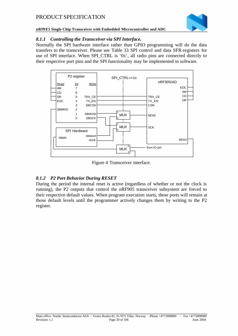
8.1.1 Controlling the Transceiver via SPI Interface.Normally the SPI hardware interface rather than GPIO programming will do the datatransfers to the transceiver. Please see Table 33 SPI control and data SFR-registers foruse of SPI interface. When SPI_CTRL is ‘0x’, all radio pins are connected directly totheir respective port pins and the SPI functionality may be implemented in software.
76543210
EOC
AM
DRCD
SBMISO
TRX_CETX_ENSBCSN
SBMOSISBSCK
P2 register
bitRead Write
SPI Hardware
EOCAM
DRCD
CSN
MOSI
SCK
MISO
TRX_CETX_EN
MUX
MUX
dataoutclock
MUX
nRF905/AD
from IO-pin
1
0
1
0
0
1
datain
SPI_CTRL==1x
Figure 4 Transceiver interface.
8.1.2 P2 Port Behavior During RESETDuring the period the internal reset is active (regardless of whether or not the clock isrunning), the P2 outputs that control the nRF905 transceiver subsystem are forced totheir respective default values. When program execution starts, these ports will remain atthose default levels until the programmer actively changes them by writing to the P2register.
PRODUCT SPECIFICATION
nRF9E5 Single Chip Transceiver with Embedded Microcontroller and ADC
Main office: Nordic Semiconductor ASA - Vestre Rosten 81, N-7075 Tiller, Norway -Phone +4772898900 - Fax +4772898989Revision: 1.1 Page 21 of 104 June 2004
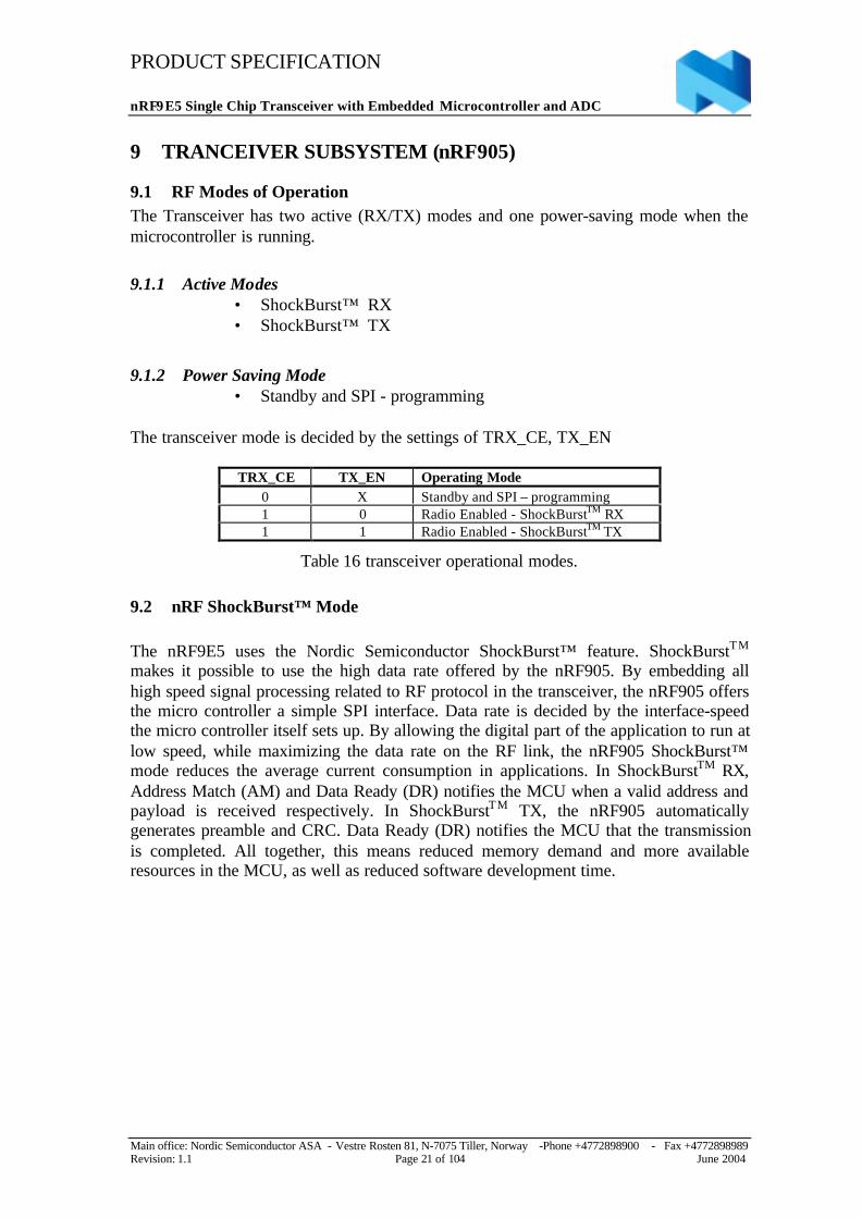
9 TRANCEIVER SUBSYSTEM (nRF905)
9.1 RF Modes of OperationThe Transceiver has two active (RX/TX) modes and one power-saving mode when themicrocontroller is running.
9.1.1 Active Modes• ShockBurst™ RX• ShockBurst™ TX
9.1.2 Power Saving Mode• Standby and SPI - programming
The transceiver mode is decided by the settings of TRX_CE, TX_EN
TRX_CE TX_EN Operating Mode0 X Standby and SPI – programming1 0 Radio Enabled - ShockBurstTM RX1 1 Radio Enabled - ShockBurstTM TX
Table 16 transceiver operational modes.
9.2 nRF ShockBurst™ Mode
The nRF9E5 uses the Nordic Semiconductor ShockBurst™ feature. ShockBurstTM
makes it possible to use the high data rate offered by the nRF905. By embedding allhigh speed signal processing related to RF protocol in the transceiver, the nRF905 offersthe micro controller a simple SPI interface. Data rate is decided by the interface-speedthe micro controller itself sets up. By allowing the digital part of the application to run atlow speed, while maximizing the data rate on the RF link, the nRF905 ShockBurst™mode reduces the average current consumption in applications. In ShockBurstTM RX,Address Match (AM) and Data Ready (DR) notifies the MCU when a valid address andpayload is received respectively. In ShockBurstTM TX, the nRF905 automaticallygenerates preamble and CRC. Data Ready (DR) notifies the MCU that the transmissionis completed. All together, this means reduced memory demand and more availableresources in the MCU, as well as reduced software development time.
PRODUCT SPECIFICATION
nRF9E5 Single Chip Transceiver with Embedded Microcontroller and ADC
Main office: Nordic Semiconductor ASA - Vestre Rosten 81, N-7075 Tiller, Norway -Phone +4772898900 - Fax +4772898989Revision: 1.1 Page 22 of 104 June 2004
Typical ShockBurstTM TX:
1. When the application MCU has data for a remote node, the address of thereceiving node (TX-address) and payload data (TX-payload) are clocked intonRF905 via the SPI interface. The application protocol or MCU sets thespeed of the interface.
2. MCU sets TRX_CE and TX_EN high, this activates a nRF905 ShockBurst™transmission.
3. nRF905 ShockBurst™:• Radio is automatically powered up.• Data package is completed (preamble added, CRC calculated).• Data package is transmitted (100kbps, GFSK, Manchester-encoded).• Data Ready is set high when transmission is completed.
4. If AUTO_RETRAN is set high, the nRF905 continuously retransmits thepackage until TRX_CE is set low.
5. When TRX_CE is set low, the nRF905 finishes transmitting the outgoingpackage and then sets itself into standby mode.
The ShockBurstTM mode ensures that a transmitted package that has started alwaysfinishes regardless of what TRX_EN and TX_EN is set to during transmission. The newmode is activated when the transmission is completed. Please see subsequent chaptersfor detailed timing
For test purposes such as antenna tuning and measuring output power it is possible to setthe transmitter so that a constant carrier is produced. To do this TRX_CE must bemaintained high instead of being pulsed. In addition Auto Retransmit should beswitched off. After the burst of data has been sent then the device will continue to sendthe unmodulated carrier.
PRODUCT SPECIFICATION
nRF9E5 Single Chip Transceiver with Embedded Microcontroller and ADC
Main office: Nordic Semiconductor ASA - Vestre Rosten 81, N-7075 Tiller, Norway -Phone +4772898900 - Fax +4772898989Revision: 1.1 Page 23 of 104 June 2004
SPI - programming
uController loading ADDRand PAYLOAD data
(Configuration register ifchanges since last TX/RX)
NO
YES
nRF ShockBurst TX
Generate CRC and preambleSending package
DR is set high when completed
Transmitteris powered
up
TRX_CE= HI ?
AUTO_RETRAN
= HI ?
YES
NO
YES
NO
ADDR PAYLOAD
Data Package
Bit in configurationregister
TRX_CE= HI ?
Radio in Standby
TX_EN = HIPWR_UP = HITRX_CE = LO
ADDR PAYLOAD CRCPre-
amble
DR isset low
after pre-amble
NB: DR is set low under the following conditions after it has been set high:• If TX_EN is set low
Figure 5 Flowchart ShockBurstTM transmit of nRF905.
PRODUCT SPECIFICATION
nRF9E5 Single Chip Transceiver with Embedded Microcontroller and ADC
Main office: Nordic Semiconductor ASA - Vestre Rosten 81, N-7075 Tiller, Norway -Phone +4772898900 - Fax +4772898989Revision: 1.1 Page 24 of 104 June 2004
Typical ShockBurstTM RX:
1. ShockBurstTM RX is selected by setting TRX_CE high and TX_EN low.2. After 650µs nRF905 is monitoring the air for incoming communication.3. When the nRF905 senses a carrier at the receiving frequency, Carrier Detect
(CD) pin is set high.4. When a valid address is received, Address Match (AM) pin is set high.5. When a valid package has been received (correct CRC found), nRF905
removes the preamble, address and CRC bits, and the Data Ready (DR) pin isset high.
6. MCU sets the TRX_CE low to enter standby mode (low current mode).7. MCU can clock out the payload data at a suitable rate via the SPI interface.8. When all payload data is retrieved, nRF905 sets Data Ready (DR) and
Address Match (AM) low again.9. The chip is now ready for entering ShockBurstTM RX, ShockBurstTM TX or
power down mode.
If TRX_CE or TX_EN is changed during an incoming package, the nRF905 changesmode immediately and the package is lost. However, if the MCU is sensing the AddressMatch (AM) pin, it knows when the chip is receiving an incoming package and cantherefore decide whether to wait for the Data Ready (DR) signal or enter a differentmode.
To avoid spurious address matches it is recommended that the address length be 24 bitsor higher in length. Small addresses such as 8 or 16 bits can often lead to statisticalfailures due to the address being repeated as part of the data packet. This can be avoidedby using a longer address.
Each byte within the address should be unique. Repeating bytes within the addressreduces the effectiveness of the address and increases its susceptibility to noise henceincreasing the packet error rate. The address should also have several level shifts (i.e.10101100) to reduce the statistical effect of noise and hence reduce the packet error rate.
PRODUCT SPECIFICATION
nRF9E5 Single Chip Transceiver with Embedded Microcontroller and ADC
Main office: Nordic Semiconductor ASA - Vestre Rosten 81, N-7075 Tiller, Norway -Phone +4772898900 - Fax +4772898989Revision: 1.1 Page 25 of 104 June 2004
Figure 6 Flowchart ShockBurstTM receive of nRF905.
NO
YES
Receiver ispowered up
NO
YES
Receivingdata
ReceiverSensing for incomming data
CD is set high if carrier
AM is sethigh
NO
DR high isset high
Radio entersSTBY
MCU clocks out payload viathe SPI interface
DR and AM are set low
YES
YES
NOAM is set low
Radio in StandbyTX_EN = LO
PWR_UP = HI
TRX_CE= HI ?
CorrectADDR?
CorrectCRC?
TRX_CE = HI ?
PAYLOAD
Data Package
ADDR PAYLOAD CRCPre-amble
RX RemainsOn
MCU clocks out payload viathe SPI interface
DR and AM are set low
PRODUCT SPECIFICATION
nRF9E5 Single Chip Transceiver with Embedded Microcontroller and ADC
Main office: Nordic Semiconductor ASA - Vestre Rosten 81, N-7075 Tiller, Norway -Phone +4772898900 - Fax +4772898989Revision: 1.1 Page 26 of 104 June 2004
9.3 Standby ModeStandby mode is used to minimize average current consumption while not transmittingor receiving and still maintaining short start up times to ShockBurstTM RX andShockBurstTM TX. In this mode the crystal oscillator have to be active. Theconfiguration word content is maintained during standby.
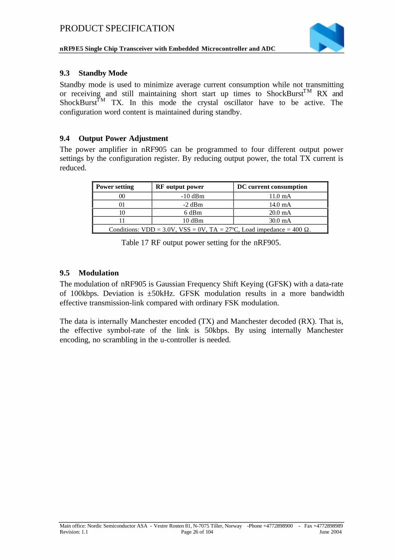
9.4 Output Power AdjustmentThe power amplifier in nRF905 can be programmed to four different output powersettings by the configuration register. By reducing output power, the total TX current isreduced.
Power setting RF output power DC current consumption00 -10 dBm 11.0 mA01 -2 dBm 14.0 mA10 6 dBm 20.0 mA11 10 dBm 30.0 mA
Conditions: VDD = 3.0V, VSS = 0V, TA = 27ºC, Load impedance = 400 Ω .
Table 17 RF output power setting for the nRF905.
9.5 ModulationThe modulation of nRF905 is Gaussian Frequency Shift Keying (GFSK) with a data-rateof 100kbps. Deviation is ±50kHz. GFSK modulation results in a more bandwidtheffective transmission-link compared with ordinary FSK modulation.
The data is internally Manchester encoded (TX) and Manchester decoded (RX). That is,the effective symbol-rate of the link is 50kbps. By using internally Manchesterencoding, no scrambling in the u-controller is needed.
PRODUCT SPECIFICATION
nRF9E5 Single Chip Transceiver with Embedded Microcontroller and ADC
Main office: Nordic Semiconductor ASA - Vestre Rosten 81, N-7075 Tiller, Norway -Phone +4772898900 - Fax +4772898989Revision: 1.1 Page 27 of 104 June 2004
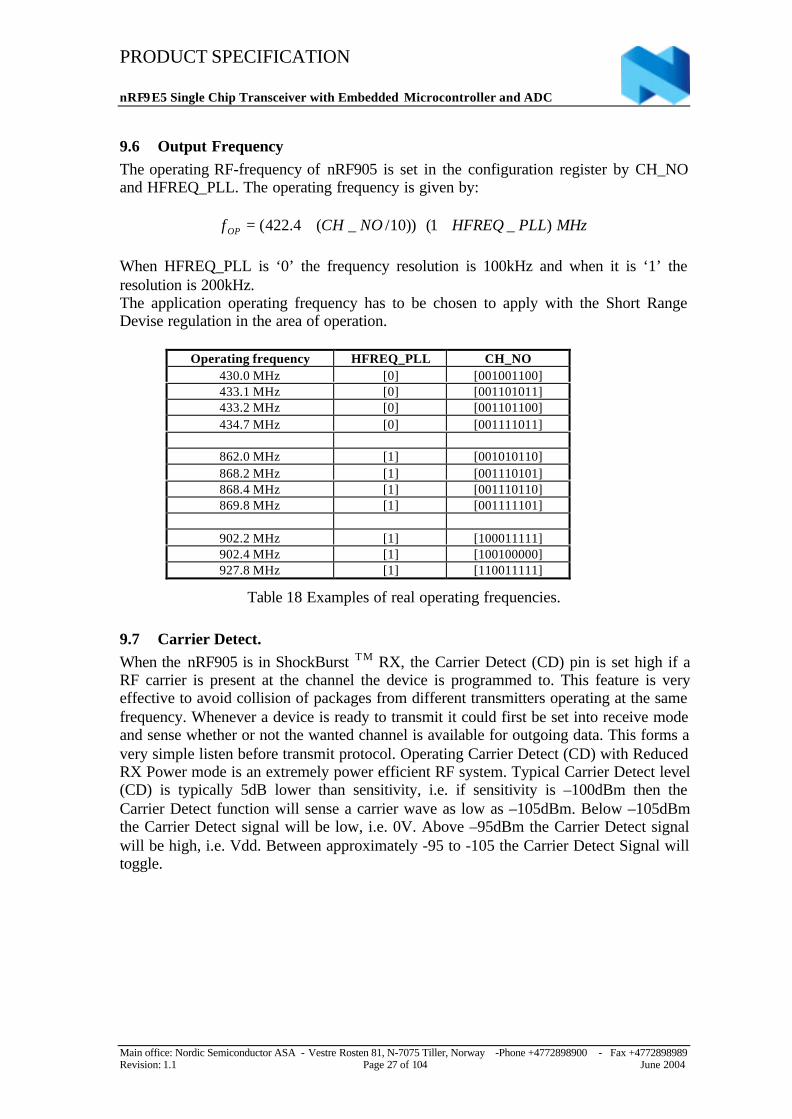
9.6 Output FrequencyThe operating RF-frequency of nRF905 is set in the configuration register by CH_NOand HFREQ_PLL. The operating frequency is given by:
MHzPLLHFREQNOCHfOP )_1())10/_(4.422( +⋅+=
When HFREQ_PLL is ‘0’ the frequency resolution is 100kHz and when it is ‘1’ theresolution is 200kHz.The application operating frequency has to be chosen to apply with the Short RangeDevise regulation in the area of operation.
Operating frequency HFREQ_PLL CH_NO430.0 MHz [0] [001001100]433.1 MHz [0] [001101011]433.2 MHz [0] [001101100]434.7 MHz [0] [001111011]
862.0 MHz [1] [001010110]868.2 MHz [1] [001110101]868.4 MHz [1] [001110110]869.8 MHz [1] [001111101]
902.2 MHz [1] [100011111]902.4 MHz [1] [100100000]927.8 MHz [1] [110011111]
Table 18 Examples of real operating frequencies.
9.7 Carrier Detect.When the nRF905 is in ShockBurst TM RX, the Carrier Detect (CD) pin is set high if aRF carrier is present at the channel the device is programmed to. This feature is veryeffective to avoid collision of packages from different transmitters operating at the samefrequency. Whenever a device is ready to transmit it could first be set into receive modeand sense whether or not the wanted channel is available for outgoing data. This forms avery simple listen before transmit protocol. Operating Carrier Detect (CD) with ReducedRX Power mode is an extremely power efficient RF system. Typical Carrier Detect level(CD) is typically 5dB lower than sensitivity, i.e. if sensitivity is –100dBm then theCarrier Detect function will sense a carrier wave as low as –105dBm. Below –105dBmthe Carrier Detect signal will be low, i.e. 0V. Above –95dBm the Carrier Detect signalwill be high, i.e. Vdd. Between approximately -95 to -105 the Carrier Detect Signal willtoggle.
PRODUCT SPECIFICATION
nRF9E5 Single Chip Transceiver with Embedded Microcontroller and ADC
Main office: Nordic Semiconductor ASA - Vestre Rosten 81, N-7075 Tiller, Norway -Phone +4772898900 - Fax +4772898989Revision: 1.1 Page 28 of 104 June 2004
9.8 Address MatchWhen the nRF905 is in ShockBurst TM RX mode, the Address Match (AM) pin is sethigh as soon as an incoming package with an address that is identical with the device’sown identity is received. With the Address Match pin the controller is alerted that thenRF905 is receiving data actually before the Data Ready (DR) signal is set high. If theData Ready (DR) pin is not set high i.e. the CRC is incorrect then the Address Match(AM) pin is reset to low at the end of the received data packet. This function can be veryuseful for an MCU. If Address Match (AM) is high then the MCU can make a decisionto wait and see if Data Ready (DR) will be set high indicating a valid data package hasbeen received or ignore that a possible package is being received and switch modes.
9.9 Data ReadyThe Data Ready (DR) signal makes it possible to largely reduce the complexity of theMCU software program.In ShockBurst TM TX, the Data Ready (DR) signal is set high when a complete packageis transmitted, telling the MCU that the nRF905 is ready for new actions. It is reset tolow at the start of a new package transmission or when switched to a different mode i.e.receive mode or standby mode.In ShockBurst TM TX Auto Retransmit the Data Ready (DR) signal is set high at thebeginning of the pre-amble and is set low at the end of the preamble. The Data Ready(DR) signal therefore pulses at the beginning of each transmitted data packet.In ShockBurst TM RX, the signal is set high when nRF905 has received a valid package,i.e. a valid address, package length and correct CRC. The MCU can then retrieve thepayload via the SPI interface. The Data Ready (DR) pin is reset to low once the data hasbeen clocked out of the data buffer or the device is switched to transmit mode.
9.10 Auto RetransmitOne way to increase system reliability in a noisy environment or in a system withoutcollision control is to transmit a package several times. This is easily accomplished withthe Auto Retransmit feature in nRF905. By setting the AUTO_RETRAN bit to “1” inthe configuration register, the circuit keeps sending the same data package as long asTRX_CE and TX_EN is high. As soon as TRX_CE is set low the device will finishsending the packet it is currently transmitting and then return to standby mode.
9.11 RX Reduced Power ModeTo maximize battery lifetime in application where the nRF905 high sensitivity is notnecessary; nRF905 offers a built in reduced power mode. In this mode, the receivecurrent consumption reduces from 12.5mA to only 10.5mA. The sensitivity is reduced totypical –85dBm, ±10dB. Some degradation of the nRF905 blocking performance shouldbe expected in this mode. The reduced power mode is an excellent option when usingCarrier Detect to sense if the wanted channel is available for outgoing data.
PRODUCT SPECIFICATION
nRF9E5 Single Chip Transceiver with Embedded Microcontroller and ADC
Main office: Nordic Semiconductor ASA - Vestre Rosten 81, N-7075 Tiller, Norway -Phone +4772898900 - Fax +4772898989Revision: 1.1 Page 29 of 104 June 2004
10 AD CONVERTER SUBSYSTEM
10.1 AD ConverterThe nRFE5 AD converter has 10 bit dynamic range and linearity when used at theNyquist rate. With lower signal frequencies and post filtering, up to 12 bits resolution ispossible. The reference for the AD converter is selectable between the AREF input andan internal 1.22V bandgap reference.
The converter default SPI setting is 10 bits. For special requirements, the AD convertercan be configured to perform 6, 8, 10 or 12 bit conversions. The converter may also beused in differential mode with AIN0 used as inverting input and one of the other 3external inputs used as noninverting input.
Two registers interface the AD converter, ADC_CONFIG_REG andADC_DATA_REG. AD converter status bit are available in the STATUS_REGISTER.Registers are described in detail in chapter 11.
Selection of input channel is directly embedded in the START_ADC_CONV command,alternatively it is set by CHSEL in the ADC_CONFIG_REG. Values of CHSEL from 0to 3 would select AIN0 to AIN3 respectively. Setting CHSEL to [1xxx] will monitor thenRF9E5 supply voltage by converting an internal input that is VDD/3 with the 1.22Vinternal reference.
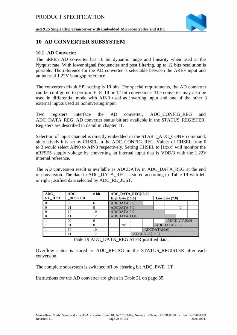
The AD conversion result is available as ADCDATA in ADC_DATA_REG at the endof conversion. The data in ADC_DATA_REG is stored according to Table 19 with leftor right justified data selected by ADC_RL_JUST.
ADC_DATA_REG[15:0]ADC_RL_JUST
ADC_RESCTRL
# bitHigh byte [15:8] Low byte [7:0]
0 00 6 ADCDATA[5:0]0 01 8 ADCDATA[7:0] ‘0’0 10 10 ADCDATA[9:0]0 11 12 ADCDATA[11:0]1 00 6 ADCDATA[5:0]1 01 8 ‘0’ ADCDATA[7:0]1 10 10 ADCDATA[9:0]1 11 12 ADCDATA[11:0]
Table 19 ADC_DATA_REGISTER justified data.
Overflow status is stored as ADC_RFLAG in the STATUS_REGISTER after eachconversion.
The complete subsystem is switched off by clearing bit ADC_PWR_UP.
Instructions for the AD converter are given in Table 21 on page 35.
PRODUCT SPECIFICATION
nRF9E5 Single Chip Transceiver with Embedded Microcontroller and ADC
Main office: Nordic Semiconductor ASA - Vestre Rosten 81, N-7075 Tiller, Norway -Phone +4772898900 - Fax +4772898989Revision: 1.1 Page 30 of 104 June 2004
10.2 AD Converter Usage
10.2.1 Measurements with External ReferenceWhen VFSSEL is set to 1 and CHSEL selects an input AINi (i.e. AIN0 to AIN3), theresult in ADCDATA is directly proportional to the ratio between the voltage on theselected input, and the voltage on pin AREF:
NAREFAINiADCDATA
VV2
⋅=
and for differential measurements a similar equation apply:
N
N
AREFAINAINiADCDATAVVV
22 )1(
0
−−⋅=−
Where N is the number of bits set in RESCTRL
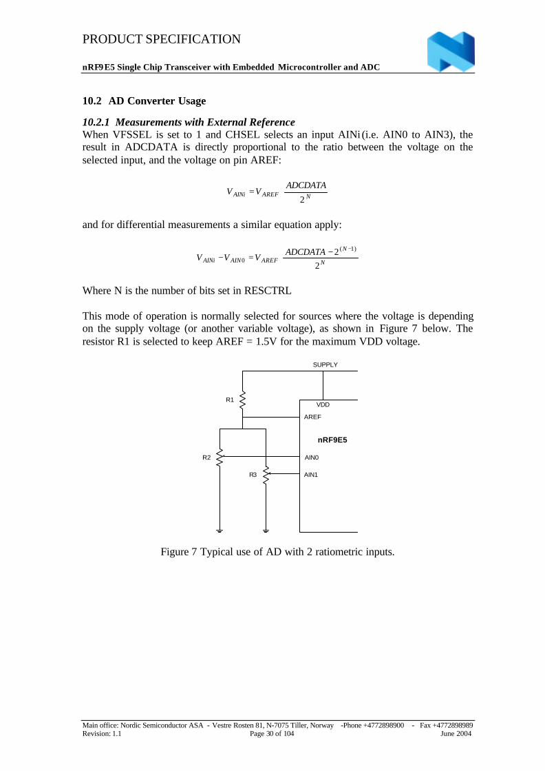
This mode of operation is normally selected for sources where the voltage is dependingon the supply voltage (or another variable voltage), as shown in Figure 7 below. Theresistor R1 is selected to keep AREF = 1.5V for the maximum VDD voltage.
R2
R3
R1
AREF
AIN0
AIN1
VDD
nRF9E5
SUPPLY
Figure 7 Typical use of AD with 2 ratiometric inputs.
PRODUCT SPECIFICATION
nRF9E5 Single Chip Transceiver with Embedded Microcontroller and ADC
Main office: Nordic Semiconductor ASA - Vestre Rosten 81, N-7075 Tiller, Norway -Phone +4772898900 - Fax +4772898989Revision: 1.1 Page 31 of 104 June 2004
10.2.2 Measurements with Internal Reference
When VFSSEL is set to 0 and CHSEL selects an input AINI (i.e. AIN0 to AIN3), theresult in ADCDATA is directly proportional to the ratio between the voltage on theselected input and the internal bandgap reference (nominally 1.22V):
NAINiADCDATA
V2
22.1 ⋅=
and for differential measurements a similar equation apply:
N
N
AINAINiADCDATAVV
2222.1
)1(
0
−−⋅=−
Where N is the number of bits set in RESCTRL
This mode of operation is normally selected for sources where the voltage is notdepending on the supply voltage.
10.2.3 Supply Voltage Measurement
When CHSEL is set to [1xxx], the ADC will use the internal bandgap reference(nominally 1.22V). The input to the converter is 1/3 of the voltage on the VDD pins.The result in ADCDATA is thus directly proportional to the VDD voltage.
NVDDADCDATA
V2
66.3 ⋅=
Where N is the number of bits set in RESCTRL
10.3 AD Converter Sampling and Timing
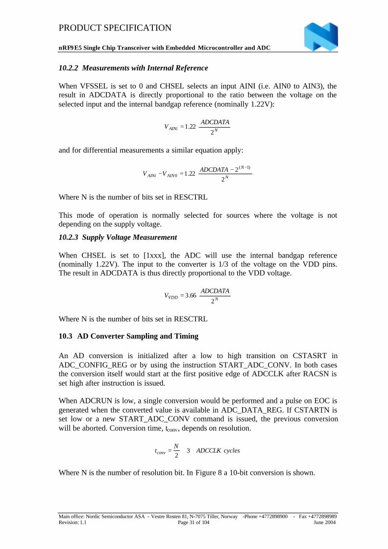
An AD conversion is initialized after a low to high transition on CSTASRT inADC_CONFIG_REG or by using the instruction START_ADC_CONV. In both casesthe conversion itself would start at the first positive edge of ADCCLK after RACSN isset high after instruction is issued.
When ADCRUN is low, a single conversion would be performed and a pulse on EOC isgenerated when the converted value is available in ADC_DATA_REG. If CSTARTN isset low or a new START_ADC_CONV command is issued, the previous conversionwill be aborted. Conversion time, tconv, depends on resolution.
cyclesADCCLKN
tconv 32
+=
Where N is the number of resolution bit. In Figure 8 a 10-bit conversion is shown.
PRODUCT SPECIFICATION
nRF9E5 Single Chip Transceiver with Embedded Microcontroller and ADC
Main office: Nordic Semiconductor ASA - Vestre Rosten 81, N-7075 Tiller, Norway -Phone +4772898900 - Fax +4772898989Revision: 1.1 Page 32 of 104 June 2004
ADCCLK
SBCSN
EOC
ADCDATA
tCONV
analogsampled
Figure 8 Timing diagram single step conversion.
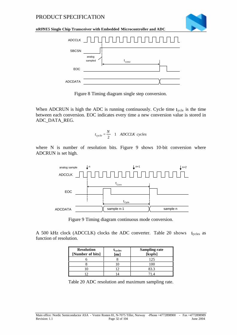
When ADCRUN is high the ADC is running continuously. Cycle time tcycle is the timebetween each conversion. EOC indicates every time a new conversion value is stored inADC_DATA_REG.
cyclesADCCLKN
tcycle 12
+=
where N is number of resolution bits. Figure 9 shows 10-bit conversion whereADCRUN is set high.
ADCCLK
EOC
ADCDATA
tConv
analog sample
tCycle
n
sample n-1 sample n
n+1 n+2
Figure 9 Timing diagram continuous mode conversion.
A 500 kHz clock (ADCCLK) clocks the ADC converter. Table 20 shows tcycles asfunction of resolution.
Resolution[Number of bits]
tcycles
[µs]Sampling rate
[kspls]6 8 1258 10 10010 12 83.312 14 71.4
Table 20 ADC resolution and maximum sampling rate.
PRODUCT SPECIFICATION
nRF9E5 Single Chip Transceiver with Embedded Microcontroller and ADC
Main office: Nordic Semiconductor ASA - Vestre Rosten 81, N-7075 Tiller, Norway -Phone +4772898900 - Fax +4772898989Revision: 1.1 Page 33 of 104 June 2004
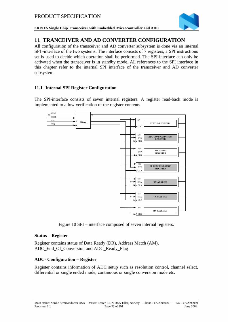
11 TRANCEIVER AND AD CONVERTER CONFIGURATIONAll configuration of the transceiver and AD converter subsystem is done via an internalSPI -interface of the two systems. The interface consists of 7 registers, a SPI instructionsset is used to decide which operation shall be performed. The SPI-interface can only beactivated when the transceiver is in standby mode. All references to the SPI interface inthis chapter refer to the internal SPI interface of the transceiver and AD convertersubsystem.
11.1 Internal SPI Register Configuration
The SPI-interface consists of seven internal registers. A register read-back mode isimplemented to allow verification of the register contents
TX-PAYLOADENDTACLK
I/O-regCSN
MOSI
MISO
SCK
RF-CONFIGURATION-REGISTER
ENDTA
CLK
TX-ADDRESS
EN
DTACLK
STATUS-REGISTER
EN
CLK
ADC-CONFIGURATION-REGISTER
ENDTACLK
RX-PAYLOADEN
CLK
ADC-DATA-REGISTER
EN
DTACLK
Figure 10 SPI – interface composed of seven internal registers.
Status – Register
Register contains status of Data Ready (DR), Address Match (AM),ADC_End_Of_Conversion and ADC_Ready_Flag
ADC- Configuration – Register
Register contains information of ADC setup such as resolution control, channel select,differential or single ended mode, continuous or single conversion mode etc.
PRODUCT SPECIFICATION
nRF9E5 Single Chip Transceiver with Embedded Microcontroller and ADC
Main office: Nordic Semiconductor ASA - Vestre Rosten 81, N-7075 Tiller, Norway -Phone +4772898900 - Fax +4772898989Revision: 1.1 Page 34 of 104 June 2004
ADC- Data – Register
Register contains AD converter results.
RF - Configuration Register
Register contains transceiver setup information such as frequency and output power ext.
TX – Address
Register contains address of target device. How many bytes used is set in theconfiguration register.
TX – Payload
Register containing the payload information to be sent in a ShockBurst TM package. Howmany bytes used is set in the configuration register.
RX – Payload
Register containing the payload information derived from a received valid ShockBurstTM package. How many bytes used is set in the configuration register. Valid data in theRX-Payload register is indicated with a high Date Ready (DR) signal.
PRODUCT SPECIFICATION
nRF9E5 Single Chip Transceiver with Embedded Microcontroller and ADC
Main office: Nordic Semiconductor ASA - Vestre Rosten 81, N-7075 Tiller, Norway -Phone +4772898900 - Fax +4772898989Revision: 1.1 Page 35 of 104 June 2004
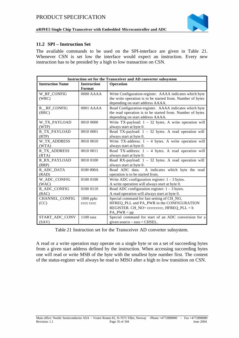
11.2 SPI – Instruction SetThe available commands to be used on the SPI-interface are given in Table 21.Whenever CSN is set low the interface would expect an instruction. Every newinstruction has to be presided by a high to low transaction on CSN.
Instruction set for the Transceiver and AD converter subsystemInstruction Name Instruction
FormatOperation
W_RF_CONFIG(WRC)
0000 AAAA Write Configuration-register. AAAA indicates which bytethe write operation is to be started from. Number of bytesdepending on start address AAAA.
R__RF_CONFIG(RRC)
0001 AAAA Read Configuration-register. AAAA indicates which bytethe read operation is to be started from. Number of bytesdepending on start address AAAA.
W_TX_PAYLOAD(WTP)
0010 0000 Write TX-payload: 1 – 32 bytes. A write operation willalways start at byte 0.
R_TX_PAYLOAD(RTP)
0010 0001 Read TX-payload: 1 – 32 bytes. A read operation willalways start at byte 0.
W_TX_ADDRESS(WTA)
0010 0010 Write TX-address: 1 – 4 bytes. A write operation willalways start at byte 0.
R_TX_ADDRESS(RTA)
0010 0011 Read TX-address: 1 – 4 bytes. A read operation willalways start at byte 0.
R_RX_PAYLOAD(RRP)
0010 0100 Read RX-payload: 1 – 32 bytes. A read operation willalways start at byte 0.
R_ADC_DATA(RAD)
0100 000A Read ADC data. A indicates which byte the readoperation is to be started from.
W_ADC_CONFIG(WAC)
0100 0100 Write ADC configuration register: 1 – 3 bytes.A write operation will always start at byte 0.
R_ADC_CONFIG(RAC)
0100 0110 Read ADC configuration register: 1 – 3 bytes.A read operation will always start at byte 0.
CHANNEL_CONFIG(CC)
1000 pphccccc cccc
Special command for fast setting of CH_NO,HFREQ_PLL and PA_PWR in the CONFIGURATIONREGISTER. CH_NO= ccccccccc, HFREQ_PLL = hPA_PWR = pp
START_ADC_CONV(SAV)
1100 ssss Special command for start of an ADC conversion for agiven source – ssss = CHSEL.
Table 21 Instruction set for the Transceiver AD converter subsystem.
A read or a write operation may operate on a single byte or on a set of succeeding bytesfrom a given start address defined by the instruction. When accessing succeeding bytesone will read or write MSB of the byte with the smallest byte number first. The contentof the status-register will always be read to MISO after a high to low transition on CSN.
PRODUCT SPECIFICATION
nRF9E5 Single Chip Transceiver with Embedded Microcontroller and ADC
Main office: Nordic Semiconductor ASA - Vestre Rosten 81, N-7075 Tiller, Norway -Phone +4772898900 - Fax +4772898989Revision: 1.1 Page 36 of 104 June 2004
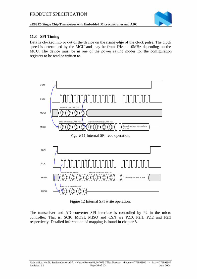
11.3 SPI TimingData is clocked into or out of the device on the rising edge of the clock pulse. The clockspeed is determined by the MCU and may be from 1Hz to 10MHz depending on theMCU. The device must be in one of the power saving modes for the configurationregisters to be read or written to.
CSN
SCK
MOSI
MISO
0 1 2 3 7 8 15
Command 8 bits, MSB = C7
C7
C6
C5
C4
C3
C2
C1
C0
Status byte as output, MSB = S7 Addressed byte as output, MSB = O7
Succeeding bytes to addressed byteas output
S7
S6
S5
S4
S3
S2
S1
S0
O7
O6
O5
O4
O3
O2
O1
O0
Figure 11 Internal SPI read operation.
CSN
SCK
MOSI
MISO
0 1 2 3 7 8 15
Command 8 bits, MSB = C7
C7
C6
C5
C4
C3
C2
C1
C0
Status byte as output, MSB = S7
S7
S6
S5
S4
S3
S2
S1
S0
D7
D6
D5
D4
D3
D2
D1
D0
First data byte as input, MSB = D7
Succeeding data bytes as input
Figure 12 Internal SPI write operation.
The transceiver and AD converter SPI interface is controlled by P2 in the microcontroller. That is, SCK, MOSI, MISO and CSN are P2.0, P2.1, P2.2 and P2.3respectively. Detailed information of mapping is found in chapter 8.
PRODUCT SPECIFICATION
nRF9E5 Single Chip Transceiver with Embedded Microcontroller and ADC
Main office: Nordic Semiconductor ASA - Vestre Rosten 81, N-7075 Tiller, Norway -Phone +4772898900 - Fax +4772898989Revision: 1.1 Page 37 of 104 June 2004
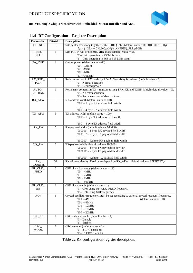
11.4 RF Configuration – Register DescriptionParameter Bitwidth Description
CH_NO 9 Sets center frequency together with HFREQ_PLL (default value = 001101100b = 108d). fRF = ( 422.4 + CH_NOd /10)*(1+HFREQ_PLLd) MHz
HFREQ_PLL
1 Sets PLL in 433 or 868/915 MHz mode (default value = 0).'0' – Chip operating in 433MHz band
'1' – Chip operating in 868 or 915 MHz bandPA_PWR 2 Output power (default value = 00).
'00' -10dBm'01' -2dBm'10' +6dBm'11' +10dBm
RX_RED_PWR
1 Reduces current in RX mode by 1.6mA. Sensitivity is reduced (default value = 0). '0' – Normal operation '1' – Reduced power
AUTO_RETRAN
1 Retransmit contents in TX – register as long TRX_CE and TXEN is high (default value = 0).'0' – No retransmission
'1' – Retransmission of data packageRX_AFW 3 RX-address width (default value = 100).
'001' – 1 byte RX address field width .'100' – 4 byte RX address field width
TX_AFW 3 TX-address width (default value = 100).'001' – 1 byte TX address field width .'100' – 4 byte TX address field width
RX_PW 6 RX-payload width (default value = 100000).'000001' – 1 byte RX payload field width'000010' – 2 byte RX payload field width .'100000' – 32 byte RX payload field width
TX_PW 6 TX-payload width (default value = 100000).'000001' – 1 byte TX payload field width'000010' – 2 byte TX payload field width .'100000' – 32 byte TX payload field width
RX_ADDRESS
32 RX address identity. Used bytes depend on RX_AFW (default value = E7E7E7E7h).
UP_CLK_FREQ
2 CPU clock frequency (default value = 11).'00' – 4MHz
'01' – 2MHz'10' – 1MHz'11' – 500kHz
UP_CLK_EN
1 CPU clock enable (default value = 1).'0' – CPU using UP_CLK_FREQ frequency'1' – CPU using XOF frequency
XOF 3 Crystal oscillator frequency. Must be set according to external crystal resonant-frequency.'000' – 4MHz (default value = 100)'001' – 8MHz'010' – 12MHz'011' – 16MHz
'100' – 20MHzCRC_EN 1 CRC – check enable (default value = 1).
'0' – Disable'1' – Enable
CRC_MODE
1 CRC – mode (default value = 1).'0' – 8 CRC check bit'1' – 16 CRC check bit
Table 22 RF configuration-register description.
PRODUCT SPECIFICATION
nRF9E5 Single Chip Transceiver with Embedded Microcontroller and ADC
Main office: Nordic Semiconductor ASA - Vestre Rosten 81, N-7075 Tiller, Norway -Phone +4772898900 - Fax +4772898989Revision: 1.1 Page 38 of 104 June 2004
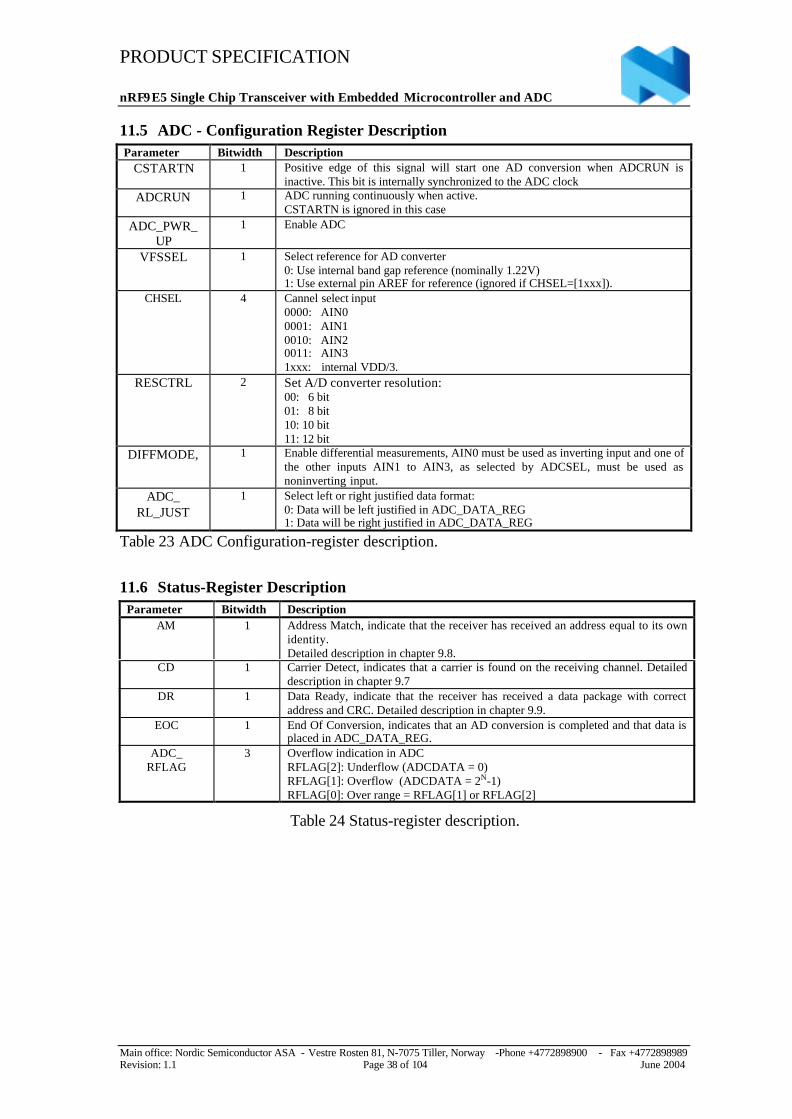
11.5 ADC - Configuration Register DescriptionParameter Bitwidth Description
CSTARTN 1 Positive edge of this signal will start one AD conversion when ADCRUN isinactive. This bit is internally synchronized to the ADC clock
ADCRUN 1 ADC running continuously when active.CSTARTN is ignored in this case
ADC_PWR_UP
1 Enable ADC
VFSSEL 1 Select reference for AD converter0: Use internal band gap reference (nominally 1.22V)1: Use external pin AREF for reference (ignored if CHSEL=[1xxx]).
CHSEL 4 Cannel select input0000: AIN00001: AIN10010: AIN20011: AIN31xxx: internal VDD/3.
RESCTRL 2 Set A/D converter resolution:00: 6 bit01: 8 bit10: 10 bit11: 12 bit
DIFFMODE, 1 Enable differential measurements, AIN0 must be used as inverting input and one ofthe other inputs AIN1 to AIN3, as selected by ADCSEL, must be used asnoninverting input.
ADC_RL_JUST
1 Select left or right justified data format:0: Data will be left justified in ADC_DATA_REG1: Data will be right justified in ADC_DATA_REG
Table 23 ADC Configuration-register description.
11.6 Status-Register DescriptionParameter Bitwidth Description
AM 1 Address Match, indicate that the receiver has received an address equal to its ownidentity.Detailed description in chapter 9.8.
CD 1 Carrier Detect, indicates that a carrier is found on the receiving channel. Detaileddescription in chapter 9.7
DR 1 Data Ready, indicate that the receiver has received a data package with correctaddress and CRC. Detailed description in chapter 9.9.
EOC 1 End Of Conversion, indicates that an AD conversion is completed and that data isplaced in ADC_DATA_REG.
ADC_RFLAG
3 Overflow indication in ADCRFLAG[2]: Underflow (ADCDATA = 0)RFLAG[1]: Overflow (ADCDATA = 2N-1)RFLAG[0]: Over range = RFLAG[1] or RFLAG[2]
Table 24 Status-register description.
PRODUCT SPECIFICATION
nRF9E5 Single Chip Transceiver with Embedded Microcontroller and ADC
Main office: Nordic Semiconductor ASA - Vestre Rosten 81, N-7075 Tiller, Norway -Phone +4772898900 - Fax +4772898989Revision: 1.1 Page 39 of 104 June 2004
11.7 RF - Register ContentsRF-CONFIG_REGISTER (R/W)
Byte # Content bit[7:0], MSB = bit[7] Init value0 CH_NO[7:0] 0110_11001 bit[7:6] not used, AUTO_RETRAN, RX_RED_PWR, PA_PWR[1:0],
HFREQ_PLL, CH_NO[8]0000_0000
2 bit[7] not used, TX_AFW[2:0] , bit[3] not used, RX_AFW[2:0] 0100_01003 bit[7:6] not used, RX_PW[5:0] 0010_00004 bit[7:6] not used, TX_PW[5:0] 0010_00005 RX_ADDRESS (device identity) byte 0 E76 RX_ADDRESS (device identity) byte 1 E77 RX_ADDRESS (device identity) byte 2 E78 RX_ADDRESS (device identity) byte 3 E79 CRC_MODE,CRC_EN, XOF[2:0], UP_CLK_EN, UP_CLK_FREQ[1:0] 1110_0111
Table 25 RF config register contents.
TX_PAYLOAD (R/W)Byte # Content bit[7:0], MSB = bit[7] Init value
0 TX_PAYLOAD[7:0] X1 TX_PAYLOAD[15:8] X- - X- - X
30 TX_PAYLOAD[247:240] X31 TX_PAYLOAD[255:248] X
Table 26 TX payload register contents.
TX_ADDRESS (R/W)Byte # Content bit[7:0], MSB = bit[7] Init value
0 TX_ADDRESS[7:0] E71 TX_ADDRESS[15:8] E72 TX_ADDRESS[23:16] E73 TX_ADDRESS[31:24] E7
Table 27 TX address register contents.
RX_PAYLOAD (R)Byte # Content bit[7:0], MSB = bit[7] Init value
0 RX_PAYLOAD[7:0] X1 RX_PAYLOAD[15:8] X
- X- X
30 RX_PAYLOAD[247:240] X31 RX_PAYLOAD[255:248] X
Table 28 RX payload register contents.
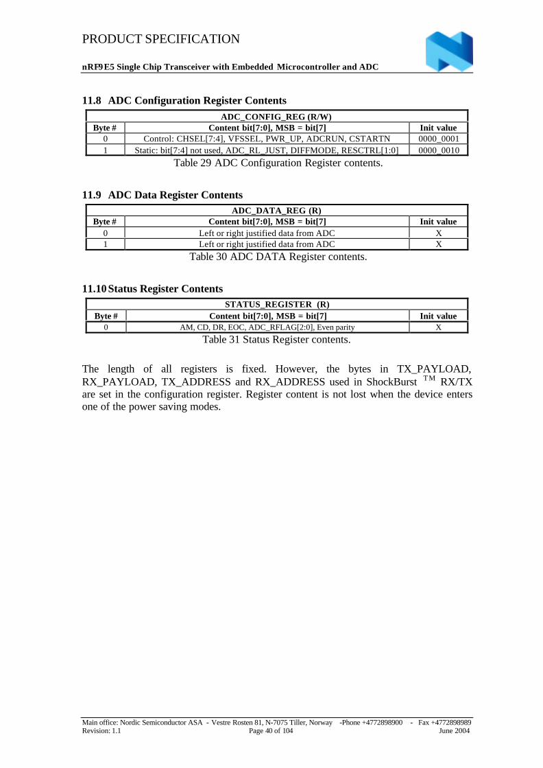
PRODUCT SPECIFICATION
nRF9E5 Single Chip Transceiver with Embedded Microcontroller and ADC
Main office: Nordic Semiconductor ASA - Vestre Rosten 81, N-7075 Tiller, Norway -Phone +4772898900 - Fax +4772898989Revision: 1.1 Page 40 of 104 June 2004
11.8 ADC Configuration Register ContentsADC_CONFIG_REG (R/W)
Byte # Content bit[7:0], MSB = bit[7] Init value0 Control: CHSEL[7:4], VFSSEL, PWR_UP, ADCRUN, CSTARTN 0000_00011 Static: bit[7:4] not used, ADC_RL_JUST, DIFFMODE, RESCTRL[1:0] 0000_0010
Table 29 ADC Configuration Register contents.
11.9 ADC Data Register ContentsADC_DATA_REG (R)
Byte # Content bit[7:0], MSB = bit[7] Init value0 Left or right justified data from ADC X1 Left or right justified data from ADC X
Table 30 ADC DATA Register contents.
11.10 Status Register ContentsSTATUS_REGISTER (R)
Byte # Content bit[7:0], MSB = bit[7] Init value0 AM, CD, DR, EOC, ADC_RFLAG[2:0], Even parity X
Table 31 Status Register contents.
The length of all registers is fixed. However, the bytes in TX_PAYLOAD,RX_PAYLOAD, TX_ADDRESS and RX_ADDRESS used in ShockBurst TM RX/TXare set in the configuration register. Register content is not lost when the device entersone of the power saving modes.
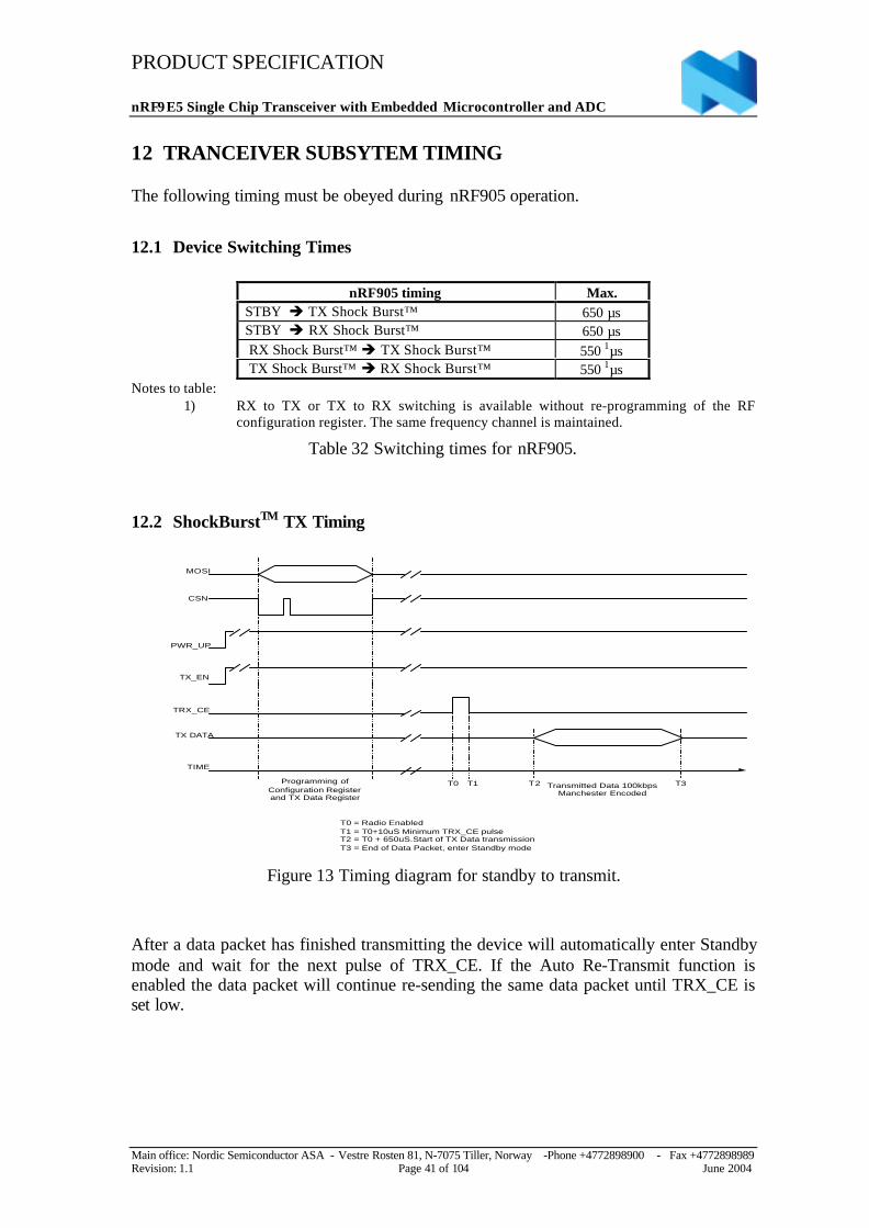
PRODUCT SPECIFICATION
nRF9E5 Single Chip Transceiver with Embedded Microcontroller and ADC
Main office: Nordic Semiconductor ASA - Vestre Rosten 81, N-7075 Tiller, Norway -Phone +4772898900 - Fax +4772898989Revision: 1.1 Page 41 of 104 June 2004
12 TRANCEIVER SUBSYTEM TIMING
The following timing must be obeyed during nRF905 operation.
12.1 Device Switching Times
nRF905 timing Max.STBY è TX Shock Burst™ 650 µsSTBY è RX Shock Burst™ 650 µs RX Shock Burst™ è TX Shock Burst™ 550 1µs TX Shock Burst™ è RX Shock Burst™ 550 1µs
Notes to table:1) RX to TX or TX to RX switching is available without re-programming of the RF
configuration register. The same frequency channel is maintained.
Table 32 Switching times for nRF905.
12.2 ShockBurstTM TX Timing
MOSI
CSN
PWR_UP
TX_EN
TRX_CE
TX DATA
TIME
T0 = Radio EnabledT1 = T0+10uS Minimum TRX_CE pulseT2 = T0 + 650uS.Start of TX Data transmissionT3 = End of Data Packet, enter Standby mode
Programming ofConfiguration Registerand TX Data Register
T0 T1 T2 T3Transmitted Data 100kbpsManchester Encoded
Figure 13 Timing diagram for standby to transmit.
After a data packet has finished transmitting the device will automatically enter Standbymode and wait for the next pulse of TRX_CE. If the Auto Re-Transmit function isenabled the data packet will continue re-sending the same data packet until TRX_CE isset low.
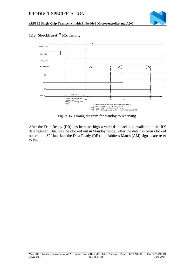
PRODUCT SPECIFICATION
nRF9E5 Single Chip Transceiver with Embedded Microcontroller and ADC
Main office: Nordic Semiconductor ASA - Vestre Rosten 81, N-7075 Tiller, Norway -Phone +4772898900 - Fax +4772898989Revision: 1.1 Page 42 of 104 June 2004
12.3 ShockBurstTM RX Timing
PWR_UP
TX_EN
TRX_CE
RX DATA
TIME
AM
DR
CD
T0 = Receiver Enabled -Listening for DataT1 = Carrier Detect finds a carrierT2 = AM - Correct Address FoundT3 = DR - Data packet with correct Address/CRC
650uS to enter RXmode fromTRX_CE being sethigh.
T0 T1 T2 T3
650uS
Figure 14 Timing diagram for standby to receiving.
After the Data Ready (DR) has been set high a valid data packet is available in the RXdata register. This may be clocked out in Standby mode. After the data has been clockedout via the SPI interface the Data Ready (DR) and Address Match (AM) signals are resetto low.
PRODUCT SPECIFICATION
nRF9E5 Single Chip Transceiver with Embedded Microcontroller and ADC
Main office: Nordic Semiconductor ASA - Vestre Rosten 81, N-7075 Tiller, Norway -Phone +4772898900 - Fax +4772898989Revision: 1.1 Page 43 of 104 June 2004
13 SPInRF9E5 SPI is a simple single buffered master. The 3 data lines of the SPI bus (MISO,SCK and MOSI) are multiplexed (by writing to register SPI_CTRL) between the GPIOpins (lower 3 bits of P1) and the RF transceiver and AD converter subsystems. The SPIhardware does not generate any chip select signal. The bootstrap loader uses EECSN(GPIO P0.3) as chip select for the boot EEPROM. On-chip GPIO P2.3 is dedicated aschip select for the RF transceiver and AD converter subsystems. GPIO pins from port 0may be used as chip selects for other external SPI slaves.
The SPI hardware is controlled by SFR’s SPI_DATA (0xb2), SPI_CTRL (0xb3) andSPICLK (0xb4) as explained in Table 33 below.
AddrSFR(hex)
R/W #bit Init(hex)
Name Function
B2 R/W 8 0 SPI_DATA SPI data input/outputB3 R/W 2 0 SPI_CTRL 00 -> SPI not used no clock generated
01 -> SPI connected to port P1 (as for booting) (see also Table 11 Port 1 (P1) functions)10 -> SPI connected to the nRF905 transceiver (see Table 15 P2 (RADIO) register )
B4 R/W 4 0 SPICLK Divider factor from CPU clock to SPI clock0000: 1/2 of CPU clock frequency0001: 1/2 of CPU clock frequency0010: 1/4 of CPU clock frequency0011: 1/8 of CPU clock frequency0100: 1/16 of CPU clock frequency0101: 1/32 of CPU clock frequency0110: 1/64 of CPU clock frequencyother: 1/64 of CPU clock frequency
Table 33 SPI control and data SFR-registers.
PRODUCT SPECIFICATION
nRF9E5 Single Chip Transceiver with Embedded Microcontroller and ADC
Main office: Nordic Semiconductor ASA - Vestre Rosten 81, N-7075 Tiller, Norway -Phone +4772898900 - Fax +4772898989Revision: 1.1 Page 44 of 104 June 2004
14 PWMThe nRF9E5 PWM output is a one-channel PWM with a 2 register interface. The firstregister, PWMCON, enables PWM function and PWM period length, which is thenumber of clock cycles for one PWM period, as shown in the table below. The otherregister, PWMDUTY, controls the duty cycle of the PWM output signal. When thisregister is written, the PWM signal will change immediately to the new value. This canresult in 4 transitions within one PWM period, but the transition period will always havea “DC value” between the “old” sample and the “new” sample.
The table shows how PWM frequency (or period length) and PWM duty cycle arecontrolled by the settings in the two PWM SFR-registers. For a crystal frequency of 16MHz, PWM frequency range will be about 1-253 kHz.
PWMCON[7:6](Number of bits)
PWM frequency PWMDUTY(duty cycle)
00 (0) 0 (PWM module inactive) 0
01 (6) [ ]( )10:5631
+⋅⋅
PWMCONf XO
[ ]63
0:5PWMDUTY
10 (7) [ ]( )10:51271
+⋅⋅
PWMCONf XO
[ ]127
0:6PWMDUTY
11 (8) [ ]( )10:52551
+⋅⋅
PWMCONf XO 255
PWMDUTY
Table 34 PWM frequency and duty-cucle.
PWM is controlled by SFR 0xA9 and 0xAA.
AddrSFR(hex)
R/W #bit Init(hex)
Name Function
A9 R/W 8 0 PWMCON PWM control register7-6: Enable / period length select 00: Disable PWM 01: Period length is 6 bit 10: Period length is 7 bit 11: Period length is 8 bit5-0: PWM frequency prescale factor (see table above)
AA R/W 8 0 PWMDUTY PWM duty cycle (6 to 8 bits according toperiod length)
Table 35 PWM control registers - SFR 0xA9 and 0xAA.
PRODUCT SPECIFICATION
nRF9E5 Single Chip Transceiver with Embedded Microcontroller and ADC
Main office: Nordic Semiconductor ASA - Vestre Rosten 81, N-7075 Tiller, Norway -Phone +4772898900 - Fax +4772898989Revision: 1.1 Page 45 of 104 June 2004
15 INTERRUPTSnRF9E5 supports the following interrupt sources:
Interruptsignal
NaturalPriority
InteruptVector
Flag Enable Control Description
INT0_N 1 0x03 TCON.1 IE.0 IP.0 External interrupt, activelow, configurable as edge-sensitive or level-sensitive,
at Port P0.3TF0 2 0x0B TCON.5 IE.1 IP.1 Timer 0 interrupt
INT1_N 3 0x13 TCON.3 IE.2 IP.2 External interrupt, activelow, configurable as edge-sensitive or level-sensitive,
at Port P0.4TF1 4 0x1B TCON.7 IE.3 IP.3 Timer 1 interrupt
TI or RI 5 0x23 SCON.0(RI),
SCON.1 (TI)
IE.4 IP.4 Receive/transmit interruptfrom Serial Port
TF2 orEXF2
6 0x2B T2CON.7(TF2),
T2CON.6(EXF2)
IE.5 IP.5 Timer 2 interrupt
int2 8 0x43 EXIF.4 EIE.0 EIP.0 Internal ADC EOC (end ofAD conversion) interrupt
int3 9 0x4B EXIF.5 EIE.1 EIP.1 Internal SPI READYinterrupt
int4 10 0x53 EXIF.6 EIE.2 EIP.2 Internal Radio Data Ready(DR) interrupt
int5 11 0x5B EXIF.7 EIE.3 EIP.3 Internal Radio AddressMatch (AM) interrupt
wdti 12 0x63 EICON.3 EIE.4 EIP.4 Internal Wakeup (GPIOwakeup and RTC timer)
interrupt
Table 36 nRF9E5 interrupt sources.
15.1 Interrupt SFRsThe following SFRs are associated with interrupt control:- IE – SFR 0xA8 (Table 37)- IP – SFR 0xB8 (Table 38)- EXIF – SFR 0x91 (Table 39)- EICON – SFR 0xD8 (Table 40)- EIE – SFR 0xE8 (Table 41)- EIP – SFR 0xF8 (Table 42)The IE and IP SFRs provide interrupt enable and priority control for the standardinterrupt unit, as with industry standard 8051. The EXIF, EICON, EIE, and EIP registersprovide flags, enable control, and priority control for the extended interrupt unit.
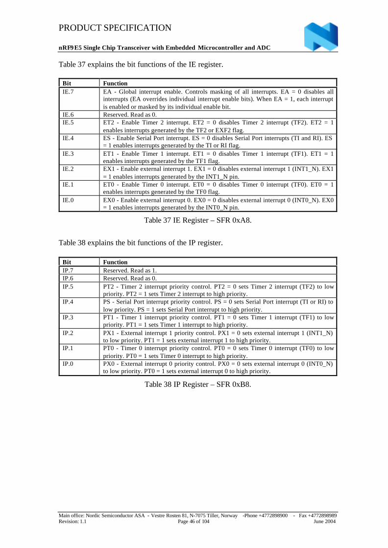
PRODUCT SPECIFICATION
nRF9E5 Single Chip Transceiver with Embedded Microcontroller and ADC
Main office: Nordic Semiconductor ASA - Vestre Rosten 81, N-7075 Tiller, Norway -Phone +4772898900 - Fax +4772898989Revision: 1.1 Page 46 of 104 June 2004
Table 37 explains the bit functions of the IE register.
Bit FunctionIE.7 EA Global interrupt enable. Controls masking of all interrupts. EA = 0 disables all
interrupts (EA overrides individual interrupt enable bits). When EA = 1, each interruptis enabled or masked by its individual enable bit.
IE.6 Reserved. Read as 0.IE.5 ET2 Enable Timer 2 interrupt. ET2 = 0 disables Timer 2 interrupt (TF2). ET2 = 1
enables interrupts generated by the TF2 or EXF2 flag.IE.4 ES Enable Serial Port interrupt. ES = 0 disables Serial Port interrupts (TI and RI). ES
= 1 enables interrupts generated by the TI or RI flag.IE.3 ET1 Enable Timer 1 interrupt. ET1 = 0 disables Timer 1 interrupt (TF1). ET1 = 1
enables interrupts generated by the TF1 flag.IE.2 EX1 Enable external interrupt 1. EX1 = 0 disables external interrupt 1 (INT1_N). EX1
= 1 enables interrupts generated by the INT1_N pin.IE.1 ET0 Enable Timer 0 interrupt. ET0 = 0 disables Timer 0 interrupt (TF0). ET0 = 1
enables interrupts generated by the TF0 flag.IE.0 EX0 Enable external interrupt 0. EX0 = 0 disables external interrupt 0 (INT0_N). EX0
= 1 enables interrupts generated by the INT0_N pin.
Table 37 IE Register – SFR 0xA8.
Table 38 explains the bit functions of the IP register.
Bit FunctionIP.7 Reserved. Read as 1.IP.6 Reserved. Read as 0.IP.5 PT2 Timer 2 interrupt priority control. PT2 = 0 sets Timer 2 interrupt (TF2) to low
priority. PT2 = 1 sets Timer 2 interrupt to high priority.IP.4 PS Serial Port interrupt priority control. PS = 0 sets Serial Port interrupt (TI or RI) to
low priority. PS = 1 sets Serial Port interrupt to high priority.IP.3 PT1 Timer 1 interrupt priority control. PT1 = 0 sets Timer 1 interrupt (TF1) to low
priority. PT1 = 1 sets Timer 1 interrupt to high priority.IP.2 PX1 External interrupt 1 priority control. PX1 = 0 sets external interrupt 1 (INT1_N)
to low priority. PT1 = 1 sets external interrupt 1 to high priority.IP.1 PT0 Timer 0 interrupt priority control. PT0 = 0 sets Timer 0 interrupt (TF0) to low
priority. PT0 = 1 sets Timer 0 interrupt to high priority.IP.0 PX0 External interrupt 0 priority control. PX0 = 0 sets external interrupt 0 (INT0_N)
to low priority. PT0 = 1 sets external interrupt 0 to high priority.
Table 38 IP Register – SFR 0xB8.
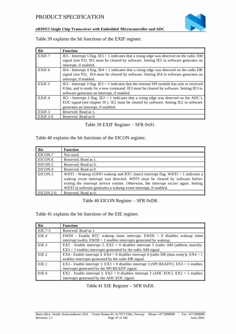
PRODUCT SPECIFICATION
nRF9E5 Single Chip Transceiver with Embedded Microcontroller and ADC
Main office: Nordic Semiconductor ASA - Vestre Rosten 81, N-7075 Tiller, Norway -Phone +4772898900 - Fax +4772898989Revision: 1.1 Page 47 of 104 June 2004
Table 39 explains the bit functions of the EXIF register.
Bit FunctionEXIF.7 IE5 Interrupt 5 flag. IE5 = 1 indicates that a rising edge was detected on the radio AM
signal (see P2). IE5 must be cleared by software. Setting IE5 in software generates aninterrupt, if enabled.
EXIF.6 IE4 Interrupt 4 flag. IE4 = 1 indicates that a rising edge was detected on the radio DRsignal (see P2). IE4 must be cleared by software. Setting IE4 in software generates aninterrupt, if enabled.
EXIF.5 IE3 Interrupt 3 flag. IE3 = 1 indicates that the internal SPI module has sent or received8 bits, and is ready for a new command. IE3 must be cleared by software. Setting IE3 insoftware generates an interrupt, if enabled.
EXIF.4 IE2 Interrupt 2 flag. IE2 = 1 indicates that a rising edge was detected on the ADC’sEOC signal (see chapter 10 ). IE2 must be cleared by software. Setting IE2 in softwaregenerates an interrupt, if enabled.
EXIF.3 Reserved. Read as 1.EXIF.20 Reserved. Read as 0.
Table 39 EXIF Register – SFR 0x91.
Table 40 explains the bit functions of the EICON register.
Bit FunctionEICON.7 Not used.EICON.6 Reserved. Read as 1.EICON.5 Reserved. Read as 0.EICON.4 Reserved. Read as 0.EICON.3 WDTI Wakeup (GPIO wakeup and RTC timer) interrupt flag. WDTI = 1 indicates a
wakeup event interrupt was detected. WDTI must be cleared by software beforeexiting the interrupt service routine. Otherwise, the interrupt occurs again. SettingWDTI in software generates a wakeup event interrupt, if enabled.
EICON.20 Reserved. Read as 0.
Table 40 EICON Register – SFR 0xD8.
Table 41 explains the bit functions of the EIE register.
Bit FunctionEIE.75 Reserved. Read as 1.EIE.4 EWDI Enable RTC wakeup timer interrupt. EWDI = 0 disables wakeup timer
interrupt (wdti). EWDI = 1 enables interrupts generated by wakeup.EIE.3 EX5 Enable interrupt 5. EX5 = 0 disables interrupt 5 (radio AM (address match)).
EX5 = 1 enables interrupts generated by the radio AM signal.EIE.2 EX4 Enable interrupt 4. EX4 = 0 disables interrupt 4 (radio DR (data ready)). EX4 = 1
enables interrupts generated by the radio DR signal.EIE.1 EX3 Enable interrupt 3. EX3 = 0 disables interrupt 3 (SPI READY). EX3 = 1 enables
interrupts generated by the SPI READY signal.EIE.0 EX2 Enable interrupt 2. EX2 = 0 disables interrupt 2 (ADC EOC). EX2 = 1 enables
interrupts generated by the ADC EOC signal.
Table 41 EIE Register – SFR 0xE8.
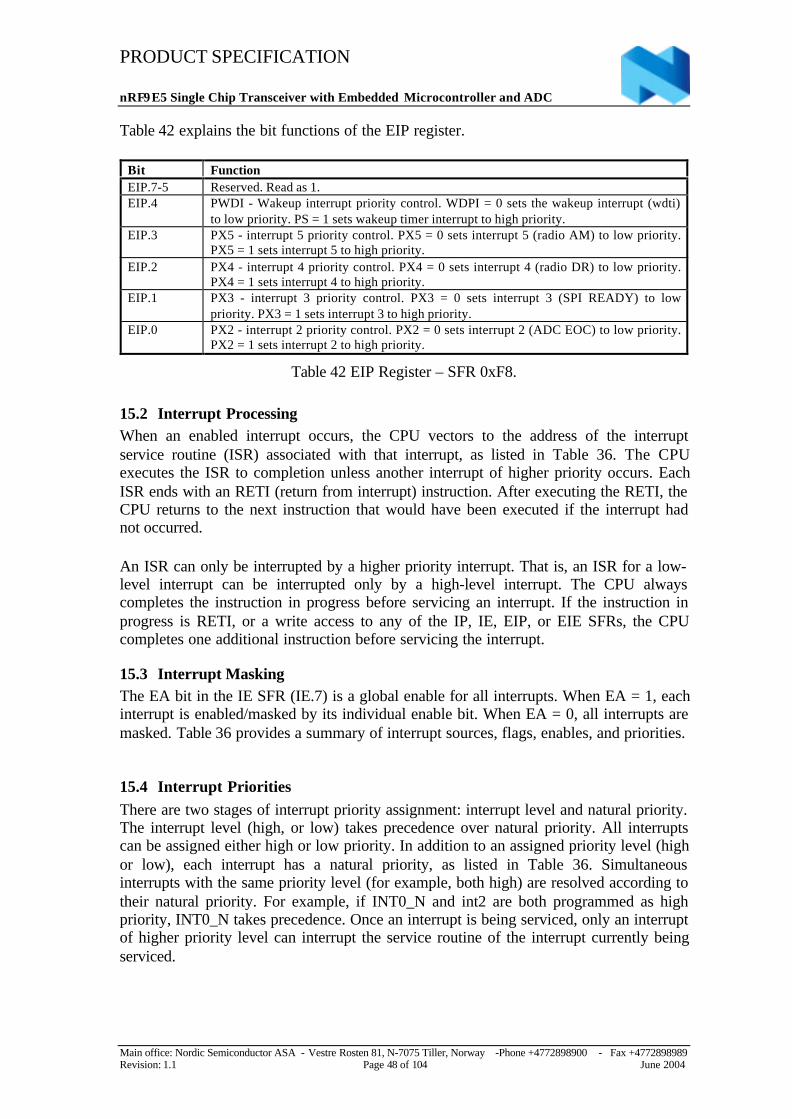
PRODUCT SPECIFICATION
nRF9E5 Single Chip Transceiver with Embedded Microcontroller and ADC
Main office: Nordic Semiconductor ASA - Vestre Rosten 81, N-7075 Tiller, Norway -Phone +4772898900 - Fax +4772898989Revision: 1.1 Page 48 of 104 June 2004
Table 42 explains the bit functions of the EIP register.
Bit FunctionEIP.75 Reserved. Read as 1.EIP.4 PWDI Wakeup interrupt priority control. WDPI = 0 sets the wakeup interrupt (wdti)
to low priority. PS = 1 sets wakeup timer interrupt to high priority.EIP.3 PX5 interrupt 5 priority control. PX5 = 0 sets interrupt 5 (radio AM) to low priority.
PX5 = 1 sets interrupt 5 to high priority.EIP.2 PX4 interrupt 4 priority control. PX4 = 0 sets interrupt 4 (radio DR) to low priority.
PX4 = 1 sets interrupt 4 to high priority.EIP.1 PX3 interrupt 3 priority control. PX3 = 0 sets interrupt 3 (SPI READY) to low
priority. PX3 = 1 sets interrupt 3 to high priority.EIP.0 PX2 interrupt 2 priority control. PX2 = 0 sets interrupt 2 (ADC EOC) to low priority.
PX2 = 1 sets interrupt 2 to high priority.
Table 42 EIP Register – SFR 0xF8.
15.2 Interrupt ProcessingWhen an enabled interrupt occurs, the CPU vectors to the address of the interruptservice routine (ISR) associated with that interrupt, as listed in Table 36. The CPUexecutes the ISR to completion unless another interrupt of higher priority occurs. EachISR ends with an RETI (return from interrupt) instruction. After executing the RETI, theCPU returns to the next instruction that would have been executed if the interrupt hadnot occurred.
An ISR can only be interrupted by a higher priority interrupt. That is, an ISR for a low-level interrupt can be interrupted only by a high-level interrupt. The CPU alwayscompletes the instruction in progress before servicing an interrupt. If the instruction inprogress is RETI, or a write access to any of the IP, IE, EIP, or EIE SFRs, the CPUcompletes one additional instruction before servicing the interrupt.
15.3 Interrupt MaskingThe EA bit in the IE SFR (IE.7) is a global enable for all interrupts. When EA = 1, eachinterrupt is enabled/masked by its individual enable bit. When EA = 0, all interrupts aremasked. Table 36 provides a summary of interrupt sources, flags, enables, and priorities.
15.4 Interrupt PrioritiesThere are two stages of interrupt priority assignment: interrupt level and natural priority.The interrupt level (high, or low) takes precedence over natural priority. All interruptscan be assigned either high or low priority. In addition to an assigned priority level (highor low), each interrupt has a natural priority, as listed in Table 36. Simultaneousinterrupts with the same priority level (for example, both high) are resolved according totheir natural priority. For example, if INT0_N and int2 are both programmed as highpriority, INT0_N takes precedence. Once an interrupt is being serviced, only an interruptof higher priority level can interrupt the service routine of the interrupt currently beingserviced.
PRODUCT SPECIFICATION
nRF9E5 Single Chip Transceiver with Embedded Microcontroller and ADC
Main office: Nordic Semiconductor ASA - Vestre Rosten 81, N-7075 Tiller, Norway -Phone +4772898900 - Fax +4772898989Revision: 1.1 Page 49 of 104 June 2004
15.5 Interrupt SamplingThe internal timers and serial port generate interrupts by setting their respective SFRinterrupt flag bits. The CPU samples external interrupts once per instruction cycle, at therising edge of CPU_clk at the end of cycle C4.The INT0_N and INT1_N signals are both active low and can be programmed throughthe IT0 and IT1 bits in the TCON SFR to be either edge-sensitive or level-sensitive. Forexample, when IT0 = 0, INT0_N is level-sensitive and the CPU sets the IE0 flag whenthe INT0_N pin is sampled low. When IT0 = 1, INT0_N is edge-sensitive and the CPUsets the IE0 flag when the INT0_N pin is sampled high then low on consecutivesamples. To ensure that edge-sensitive interrupts are detected, the corresponding portsshould be held high for four clock cycles and then low for four clock cycles. Level-sensitive interrupts are not latched and must remain active until serviced.
PRODUCT SPECIFICATION
nRF9E5 Single Chip Transceiver with Embedded Microcontroller and ADC
Main office: Nordic Semiconductor ASA - Vestre Rosten 81, N-7075 Tiller, Norway -Phone +4772898900 - Fax +4772898989Revision: 1.1 Page 50 of 104 June 2004
15.6 Interrupt LatencyInterrupt response time depends on the current state of the CPU. The fastest responsetime is five instruction cycles: one to detect the interrupt, and four to perform theLCALL to the ISR. The maximum latency (thirteen instruction cycles) occurs when theCPU is currently executing an RETI instruction followed by a MUL or DIV instruction.The thirteen instruction cycles in this case are: one to detect the interrupt, three tocomplete the RETI, five to execute the DIV or MUL, and four to execute the LCALL tothe ISR.For the maximum latency case, the response time is 13 x 4 = 52clock cycles.
15.7 Interrupt Latency from Power Down State.The nRF9E5 may be set into Power Down state by writing a non zero value to SFR0xB6, register CK_CTRL. The CPU will then perform a controlled shutdown of clockand power regulator depending on what mode was selected. The system can only berestarted from an RTC wakeup, a GPIO wakeup or a Watchdog reset. If a wakeupinterrupt is enabled, the startup time for regulators and clocks will be added to theinterrupt latency. See 17.2.1 Startup Time From Reset
15.8 Single-Step OperationThe nRF9E5 interrupt structure provides a way to perform single-step programexecution. When exiting an ISR with an RETI instruction, the CPU will always executeat least one instruction of the task program. Therefore, once an ISR is entered, it cannotbe re-entered until at least one program instruction is executed. To perform single-stepexecution, program one of the external interrupts (for example, INT0_N) to be levelsensitive and write an ISR for that interrupt that terminates as follows:
JNB TCON.1,$ ; wait for high on INT0_NJB TCON.1,$ ; wait for low on INT0_NRETI ; return for ISR
The CPU enters the ISR when INT0_N goes low, then waits for a pulse on INT0_N.Each time INT0_N is pulsed, the CPU exits the ISR, executes one program instruction,then re-enters the ISR.
PRODUCT SPECIFICATION
nRF9E5 Single Chip Transceiver with Embedded Microcontroller and ADC
Main office: Nordic Semiconductor ASA - Vestre Rosten 81, N-7075 Tiller, Norway -Phone +4772898900 - Fax +4772898989Revision: 1.1 Page 51 of 104 June 2004
16 LF CLOCK WAKEUP FUNCTIONS AND WATCHDOG
16.1 The LF ClockThe nRF9E5 contains has an internal low frequency clock CKLF that is always active.When the crystal oscillator clocks the circuit, the CKLF is a 4kHz clock derived fromthe crystal oscillator (provided the CKLFCON register is set according to crystalfrequency and prescaler. XOF and UP_CLK_FREQ respectively, see Table 22). Whenno crystal oscillator clock is available, the CKLF is a low power RC oscillator(LP_OSC) that cannot be disabled, so it will run continuously as long as VDD = 1.8V.
The microprocessor can determine the phase of the CKLF clock by reading CK_CTRLSFR 0xB6, see Table 50.
16.2 Tick CalibrationThe “TICK” is an interval (in CKLF periods) that determines the resolution of thewatchdog and the RTC wakeup timer. The tick is nominally 1ms (4 CKLF cycles).When the CPU is active and in power down modes where the chip still has crystal clock,the “TICK” will be as accurate as the crystal oscillator. When the CKLF switches to theRC oscillator (LP_OSC) in deep power down modes, the tick will no longer be accurate.The LP_OSC clock source is very inaccurate, and may vary from 0.5ms to 3msdepending production lot, temperature and supply voltage. That means that Watchdogand RTC wakeup may not be used for any accurate timing functions if these powerdown modes are used.
The accuracy can be improved by calibrating the TICK value at regular intervals. Theregister TICK_DV controls how many LP_OSC periods elapse between each TICK. Thefrequency of the LP_OSC (between 1 kHz and 5 kHz) can be measured by timer2 incapture mode with t2ex enabled (EXEN2=1). The signal connected to t2ex has exactlyhalf the frequency of LP_OSC. The 16-bit difference between two consecutive capturesin SFR-registersRCAP2H,RCAP2L is proportional to the LP_OSC period. For detailsabout timer2 see ch. 18.8.3 and Figure 21 Timer 2 – Timer/Counter with Capture
TICK is controlled by SFRs 0xB5 and 0xBF
AddrSFR
R/W #bit InitHex
Name Function
B5 R/W 8 03 TICK_DV Divider that’s used in generating TICK from CKLFfrequency.TTICK = (1 + TICK_DV) / fCKLF
The default value gives a TICK of 1ms nominal asdefault (with CKLF derived from crystal oscillator).
BF R/W 6 27 CKLFCON Configure CKLF generation with crystal frequencyand prescaler value. Note this register only controls thegeneration of CKLF, not the actual prescaler values.5-3: Should be set equal to XOF, Table 222: Should be set equal to UP_CLK_EN, Table 221-0: Should be set equal to UP_CLK_FREQ, Table 22
Table 43 TICK control register - SFR 0xB5.
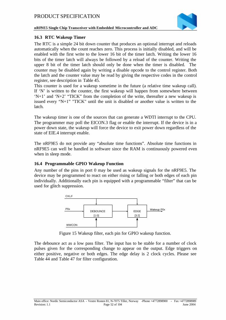
PRODUCT SPECIFICATION
nRF9E5 Single Chip Transceiver with Embedded Microcontroller and ADC
Main office: Nordic Semiconductor ASA - Vestre Rosten 81, N-7075 Tiller, Norway -Phone +4772898900 - Fax +4772898989Revision: 1.1 Page 52 of 104 June 2004
16.3 RTC Wakeup TimerThe RTC is a simple 24 bit down counter that produces an optional interrupt and reloadsautomatically when the count reaches zero. This process is initially disabled, and will beenabled with the first write to the lower 16 bit of the timer latch. Writing the lower 16bits of the timer latch will always be followed by a reload of the counter. Writing theupper 8 bit of the timer latch should only be done when the timer is disabled. Thecounter may be disabled again by writing a disable opcode to the control register. Boththe latch and the counter value may be read by giving the respective codes in the controlregister, see description in Table 45.This counter is used for a wakeup sometime in the future (a relative time wakeup call).If ‘N’ is written to the counter, the first wakeup will happen from somewhere between‘N+1’ and ‘N+2’ “TICK” from the completion of the write, thereafter a new wakeup isissued every “N+1” "TICK" until the unit is disabled or another value is written to thelatch.
The wakeup timer is one of the sources that can generate a WDTI interrupt to the CPU.The programmer may poll the EICON.3 flag or enable the interrupt. If the device is in apower down state, the wakeup will force the device to exit power down regardless of thestate of EIE.4 interrupt enable.
The nRF9E5 do not provide any “absolute time functions”. Absolute time functions innRF9E5 can well be handled in software since the RAM is continuously powered evenwhen in sleep mode.
16.4 Programmable GPIO Wakeup FunctionAny number of the pins in port 0 may be used as wakeup signals for the nRF9E5. Thedevice may be programmed to react on either rising or falling or both edges of each pinindividually. Additionally each pin is equipped with a programmable “filter” that can beused for glitch suppression.
DEBOUNCE EDGE
WWCON
CKLF
P0x
[1:0] [3:2]
Wakeup P0x
Figure 15 Wakeup filter, each pin for GPIO wakeup function.
The debounce act as a low pass filter. The input has to be stable for a number of clockpulses given for the corresponding change to appear on the output. Edge triggers oneither positive, negative or both edges. The edge delay is 2 clock cycles. Please seeTable 44 and Table 47 for filter configuration.
PRODUCT SPECIFICATION
nRF9E5 Single Chip Transceiver with Embedded Microcontroller and ADC
Main office: Nordic Semiconductor ASA - Vestre Rosten 81, N-7075 Tiller, Norway -Phone +4772898900 - Fax +4772898989Revision: 1.1 Page 53 of 104 June 2004
Filter selection Debounce Edge detector selectionWCON [1:0] Number of clock pulses WCON [3:2] pos / neg trigger
00 0 00 Off01 2 01 Pos10 8 10 Neg11 64 11 Both
Table 44 GPIO wakeup filter configuration.
16.5 WatchdogThe watchdog is activated on the first write to its control register SFR 0xAD. It can notbe disabled by any other means than a reset. The watchdog register is loaded by writinga 16-bit value to the two 8-bit data registers (SFR 0xAB and 0xAC) and then the writingthe correct opcode to the control register. The watchdog will then count down towards 0and when 0 is reached the complete microcontroller will be reset To avoid the reset, thesoftware must load new values into the watchdog register sufficiently often.
16.6 Programming Interface to Watchdog and Wakeup FunctionsFigure 16 shows how the blocks that are always active are connected to the CPU. RTCtimer GPIO wakeup and Watchdog are controlled via SFRs 0xAB, 0xAC and 0xAD.These 3 registers REGX_MSB, REGX_LSB and REGX_CTRL are used to interface theblocks running on the slow CKLF clock. The 16-bit register REGX_MSB,REGX_LSB can be written or read as two bytes from the CPU.
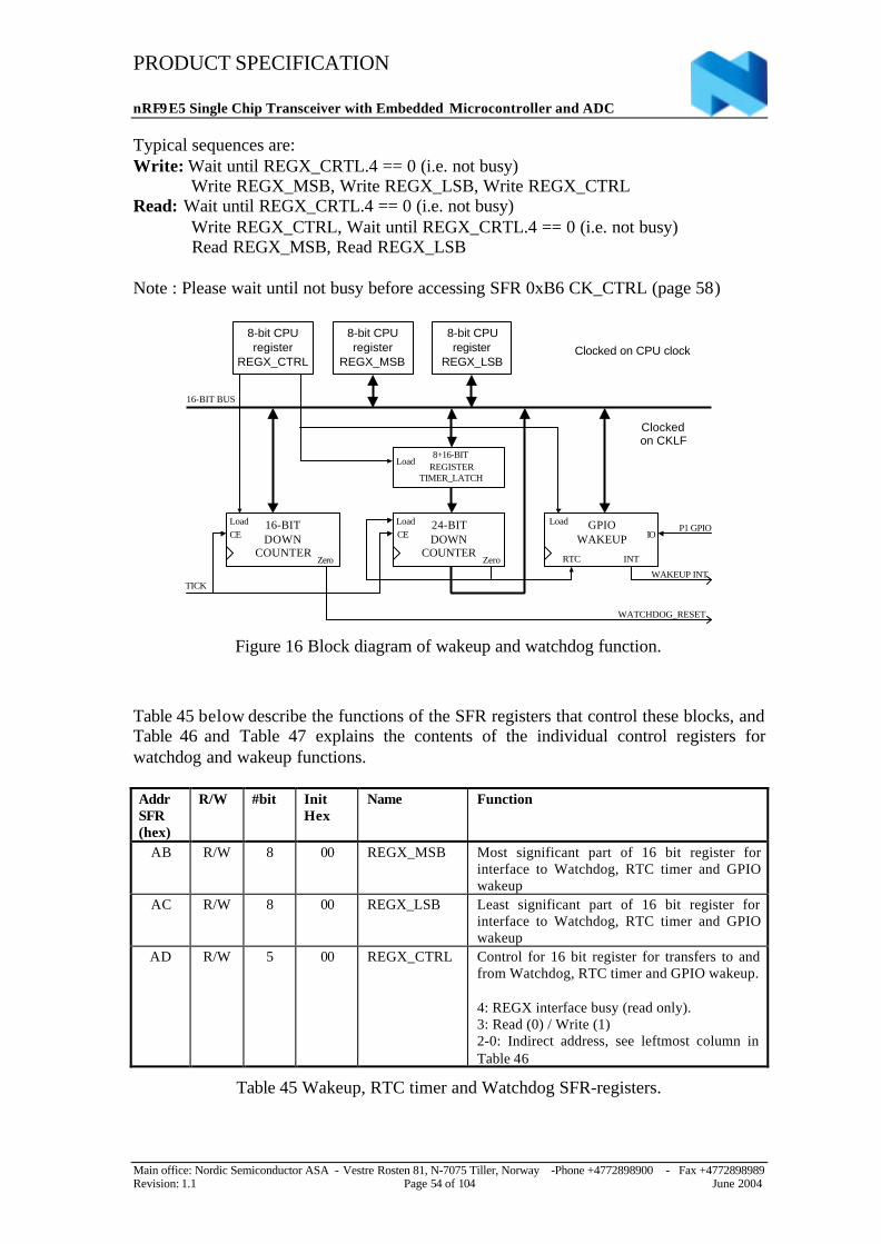
PRODUCT SPECIFICATION
nRF9E5 Single Chip Transceiver with Embedded Microcontroller and ADC
Main office: Nordic Semiconductor ASA - Vestre Rosten 81, N-7075 Tiller, Norway -Phone +4772898900 - Fax +4772898989Revision: 1.1 Page 54 of 104 June 2004
Typical sequences are:Write: Wait until REGX_CRTL.4 == 0 (i.e. not busy)
Write REGX_MSB, Write REGX_LSB, Write REGX_CTRLRead: Wait until REGX_CRTL.4 == 0 (i.e. not busy)
Write REGX_CTRL, Wait until REGX_CRTL.4 == 0 (i.e. not busy) Read REGX_MSB, Read REGX_LSB
Note : Please wait until not busy before accessing SFR 0xB6 CK_CTRL (page 58)
TICKWAKEUP INT
WATCHDOG_RESET
8+16-BITREGISTER
TIMER_LATCH
8-bit CPUregister
REGX_LSB
8-bit CPUregister
REGX_MSB
8-bit CPUregister
REGX_CTRL
Load
16-BIT BUS
24-BITDOWN
COUNTERZero
Load16-BITDOWN
COUNTERZero
LoadCE
GPIOWAKEUP IO
RTC INT
P1 GPIOCE
Load
Clocked on CPU clock
Clockedon CKLF
Figure 16 Block diagram of wakeup and watchdog function.
Table 45 below describe the functions of the SFR registers that control these blocks, andTable 46 and Table 47 explains the contents of the individual control registers forwatchdog and wakeup functions.
AddrSFR(hex)
R/W #bit InitHex
Name Function
AB R/W 8 00 REGX_MSB Most significant part of 16 bit register forinterface to Watchdog, RTC timer and GPIOwakeup
AC R/W 8 00 REGX_LSB Least significant part of 16 bit register forinterface to Watchdog, RTC timer and GPIOwakeup
AD R/W 5 00 REGX_CTRL Control for 16 bit register for transfers to andfrom Watchdog, RTC timer and GPIO wakeup.
4: REGX interface busy (read only).3: Read (0) / Write (1)2-0: Indirect address, see leftmost column inTable 46
Table 45 Wakeup, RTC timer and Watchdog SFR-registers.
PRODUCT SPECIFICATION
nRF9E5 Single Chip Transceiver with Embedded Microcontroller and ADC
Main office: Nordic Semiconductor ASA - Vestre Rosten 81, N-7075 Tiller, Norway -Phone +4772898900 - Fax +4772898989Revision: 1.1 Page 55 of 104 June 2004
AddrCtrl[2:0]
R/WCtrl [3]
#bit InitHex
Name Function
0 16 0000 RWD Watchdog register (count)0 1 16 0000 WWD Watchdog register (count)
0 16 0000 RGTIMER 15-8: MSB part of RTC counter7-0: MSB part of RTC latch
11 12 000 WGTIMER 11-8: GTIMER latch
7-0: MSB part of RTC latch0 16 0000 RRTCLAT Least significant part of RTC latch
21 16 0000 WRTCLAT Least significant part of RTC latch0 16 0000 RRTC RTC counter value
3 1 0 - WRTCDIS Disable RTC (data not used)
0 9 000 RWSTA0 Wakeup statusBit 8: RTC timer status7-0: Wakeup status for pins P07-P00
4
1 16 0000 WWCON0 GPIO wakeup configuration forP03-P00. See Table 47.
0 9 000 RWSTA1 Wakeup status (Identical to WSTA0)5 1 16 0000 WWCON1 GPIO wakeup configuration for
P07-P04. See Table 47.
Table 46 Indirect addresses and functions.
Bits WWCON1 function WWCON0 unction15:14 Edge selection for P07 Edge selection for P0313:12 Edge filter for P07 Edge filter for P0311:10 Edge selection for P06 Edge selection for P02
9:8 Edge filter for P06 Edge filter for P027:6 Edge selection for P05 Edge selection for P015:4 Edge filter for P05 Edge filter for P013:2 Edge selection for P04 Edge selection for P001:0 Edge filter for P04 Edge filter for P00
Table 47 Bit fields in register WWCON1 and WWCON0.
16.7 ResetThe nRF9E5 can be reset either by the on-chip power-on reset circuitry or by the on-chip watchdog counter.
16.7.1 Power-on ResetThe power-on reset circuitry keeps the chip in power-on-reset state until the supplyvoltage reaches VDDmin (a voltage, less than 1.9V sufficiently high for digitaloperation). At this point the internal voltage generators and oscillators start up, the SFRsare initialized to their reset values, as listed in Table 62, and thereafter the CPU beginsprogram execution at the standard reset vector address 0x0000. The startup time frompower-on reset is normally determined by both the crystal oscillator startup time and thefrequency of the low power oscillator (LP_OSC). This total may vary from 1 to 3 msdepending on processing, temperature and supply voltage.
PRODUCT SPECIFICATION
nRF9E5 Single Chip Transceiver with Embedded Microcontroller and ADC
Main office: Nordic Semiconductor ASA - Vestre Rosten 81, N-7075 Tiller, Norway -Phone +4772898900 - Fax +4772898989Revision: 1.1 Page 56 of 104 June 2004
16.7.2 Watchdog ResetIf the Watchdog reset signal goes active, nRF9E5 enters the same reset sequence as forpower-on reset. That is, the internal voltage generators and oscillators start up, the SFRsare initialized to their reset values, as listed in Table 62, and thereafter the CPU beginsprogram execution at the standard reset vector address 0x0000. The startup time fromwatchdog reset is somewhat shorter; expect a variation from 0.4 to 2ms depending onprocessing, temperature and supply voltage.
16.7.3 Program Reset AddressThe program reset address is controlled by the RSTREAS register, SFR 0xB1, see Table48This register shows which reset source that caused the last reset, and provides achoice of two different program start addresses. The default value is power-on reset,which starts the boot loader, while a watchdog reset does not reboot and restarts ataddress 0 of the already loaded program.
AddrSFR(hex)
R/W #bit Init(hex)
Name Function
B1 R/W 2 02 RSTREAS bit 0: Reason for last reset 0: POR 1: Any other reset source Clear this bit in software to force a reboot after jump to zero (boot loader will load code RAM if this bit is 0)bit 1: Use IROM for reset vector 0: Reset vectors to 0x0000. 1: Reset vectors to 0x8000.
Table 48 Reset control register - SFR 0xB1.
PRODUCT SPECIFICATION
nRF9E5 Single Chip Transceiver with Embedded Microcontroller and ADC
Main office: Nordic Semiconductor ASA - Vestre Rosten 81, N-7075 Tiller, Norway -Phone +4772898900 - Fax +4772898989Revision: 1.1 Page 57 of 104 June 2004
17 POWER SAVING MODESnRF9E5 provides the two industry standard 8051 power saving modes: idle mode andstop mode. To Achieve more power saving several additional power-down modes areprovided, where both oscillator and internal power regulators may be turned off.
The bits that control entry into idle and stop modes are in the PCON register at SFRaddress 0x87, listed in Table 49. The bits that control entry into power down mode are inthe CK_CTRL register at SFR address 0xB6, listed in Table 51.
Bit FunctionPCON.7 SMOD – Serial Port baud-rate doubler enable. When SMOD = 1, the baud rate for
Serial Port is doubled.PCON.6–4 Reserved.PCON.3 GF1 – General purpose flag 1. Bit-addressable, general purpose flag for software
control.PCON.2 GF0 – General purpose flag 0. Bit-addressable, general purpose flag for software
control.PCON.1 STOP – Stop mode select. Setting the STOP bit places the nRF9E5 in stop mode.PCON.0 IDLE – Idle mode select. Setting the IDLE bit places the nRF9E5 in idle mode.
Table 49 PCON Register – SFR 0x87.
17.1 Standard 8051 Power Saving Modes
17.1.1 Idle ModeAn instruction that sets the IDLE bit (PCON.0) causes the nRF9E5 to enter idle modewhen that instruction completes. In idle mode, CPU processing is suspended and internalregisters and memory maintain their current data. However, unlike the standard 8051,the CPU clock is not disabled internally, thus not much power is saved.There are two ways to exit idle mode: activate any enabled interrupt or watchdog reset.Activation of any enabled interrupt causes the hardware to clear the IDLE bit andterminate idle mode. The CPU executes the ISR associated with the received interrupt.The RETI instruction at the end of the ISR returns the CPU to the instruction followingthe one that put the nRF9E5 into idle mode. A watchdog reset causes the nRF9E5 to exitidle mode, reset internal registers, execute its reset sequence and begin programexecution at the standard reset vector address 0x0000.
17.1.2 Stop ModeAn instruction that sets the STOP bit (PCON.1) causes the nRF9E5 to enter stop modewhen that instruction completes. Stop mode is identical to idle mode, except that theonly way to exit stop mode is by watchdog reset Since there is little power saving, stopmode is not recommended, as it is more efficient to use power down mode.
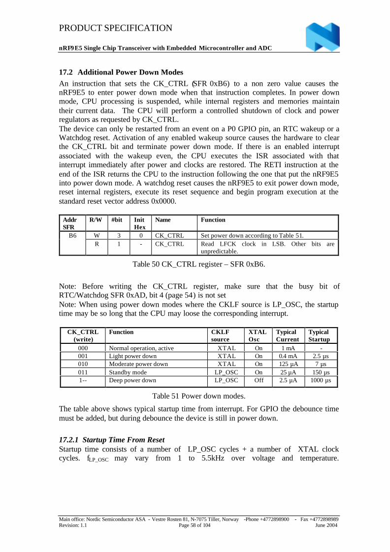
PRODUCT SPECIFICATION
nRF9E5 Single Chip Transceiver with Embedded Microcontroller and ADC
Main office: Nordic Semiconductor ASA - Vestre Rosten 81, N-7075 Tiller, Norway -Phone +4772898900 - Fax +4772898989Revision: 1.1 Page 58 of 104 June 2004
17.2 Additional Power Down ModesAn instruction that sets the CK_CTRL (SFR 0xB6) to a non zero value causes thenRF9E5 to enter power down mode when that instruction completes. In power downmode, CPU processing is suspended, while internal registers and memories maintaintheir current data. The CPU will perform a controlled shutdown of clock and powerregulators as requested by CK_CTRL.The device can only be restarted from an event on a P0 GPIO pin, an RTC wakeup or aWatchdog reset. Activation of any enabled wakeup source causes the hardware to clearthe CK_CTRL bit and terminate power down mode. If there is an enabled interruptassociated with the wakeup even, the CPU executes the ISR associated with thatinterrupt immediately after power and clocks are restored. The RETI instruction at theend of the ISR returns the CPU to the instruction following the one that put the nRF9E5into power down mode. A watchdog reset causes the nRF9E5 to exit power down mode,reset internal registers, execute its reset sequence and begin program execution at thestandard reset vector address 0x0000.
AddrSFR
R/W #bit InitHex
Name Function
W 3 0 CK_CTRL Set power down according to Table 51.B6R 1 - CK_CTRL Read LFCK clock in LSB. Other bits are
unpredictable.
Table 50 CK_CTRL register – SFR 0xB6.
Note: Before writing the CK_CTRL register, make sure that the busy bit ofRTC/Watchdog SFR 0xAD, bit 4 (page 54) is not setNote: When using power down modes where the CKLF source is LP_OSC, the startuptime may be so long that the CPU may loose the corresponding interrupt.
CK_CTRL(write)
Function CKLFsource
XTALOsc
TypicalCurrent
TypicalStartup
000 Normal operation, active XTAL On 1 mA -001 Light power down XTAL On 0.4 mA 2.5 µs010 Moderate power down XTAL On 125 µA 7 µs011 Standby mode LP_OSC On 25 µA 150 µs1-- Deep power down LP_OSC Off 2.5 µA 1000 µs
Table 51 Power down modes.
The table above shows typical startup time from interrupt. For GPIO the debounce timemust be added, but during debounce the device is still in power down.
17.2.1 Startup Time From ResetStartup time consists of a number of LP_OSC cycles + a number of XTAL clockcycles. fLP_OSC may vary from 1 to 5.5kHz over voltage and temperature.
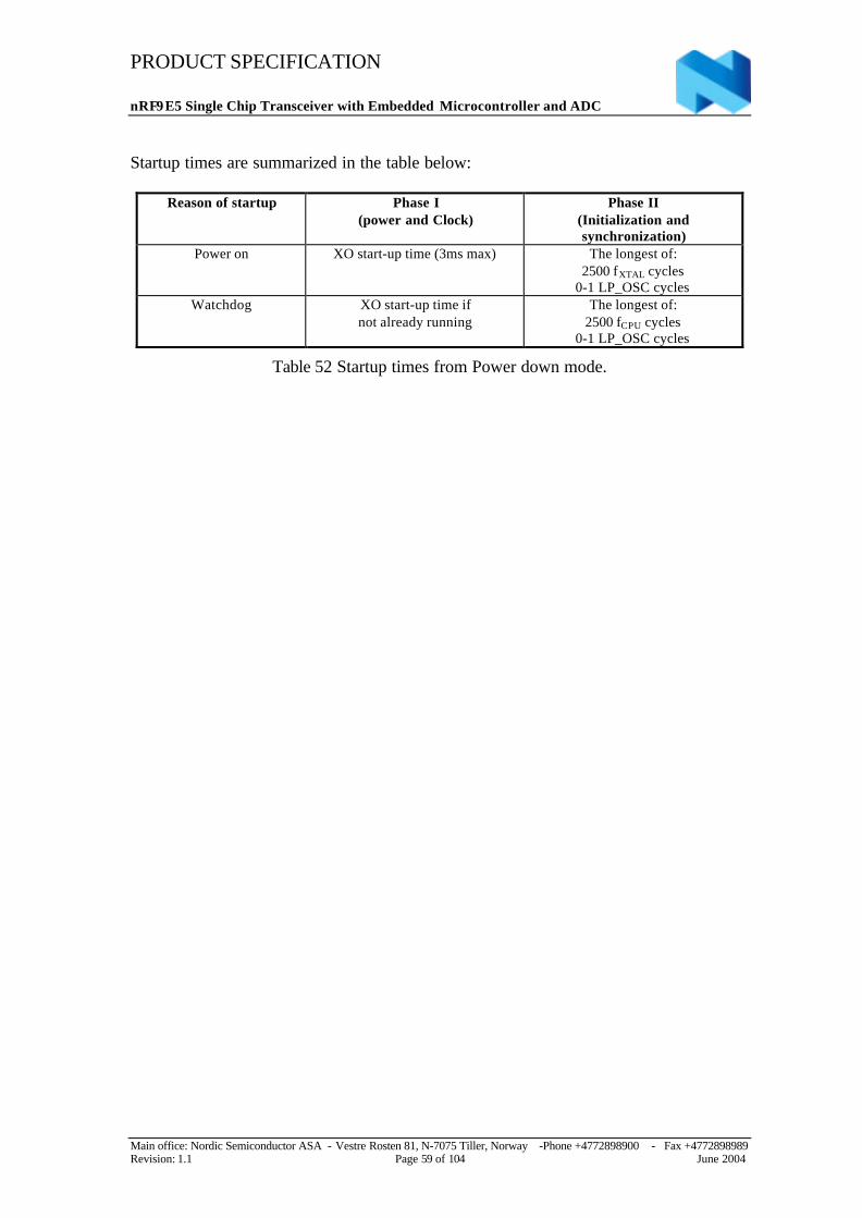
PRODUCT SPECIFICATION
nRF9E5 Single Chip Transceiver with Embedded Microcontroller and ADC
Main office: Nordic Semiconductor ASA - Vestre Rosten 81, N-7075 Tiller, Norway -Phone +4772898900 - Fax +4772898989Revision: 1.1 Page 59 of 104 June 2004
Startup times are summarized in the table below:
Reason of startup Phase I(power and Clock)
Phase II(Initialization andsynchronization)
Power on XO start-up time (3ms max) The longest of:2500 fXTAL cycles
0-1 LP_OSC cyclesWatchdog XO start-up time if
not already runningThe longest of:
2500 fCPU cycles0-1 LP_OSC cycles
Table 52 Startup times from Power down mode.
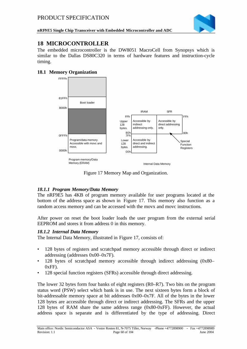
PRODUCT SPECIFICATION
nRF9E5 Single Chip Transceiver with Embedded Microcontroller and ADC
Main office: Nordic Semiconductor ASA - Vestre Rosten 81, N-7075 Tiller, Norway -Phone +4772898900 - Fax +4772898989Revision: 1.1 Page 60 of 104 June 2004
18 MICROCONTROLLERThe embedded microcontroller is the DW8051 MacroCell from Synopsys which issimilar to the Dallas DS80C320 in terms of hardware features and instruction-cycletiming.
18.1 Memory Organization
Boot loader
Program/data memory.Accessible with movc andmovx.
0000h
0FFFh
8000h
81FFh
FFFFh
Accessible bydirect and indirectaddressing.
Accessible bydirect addressingonly.
Accessible byindirectaddressing only.
Internal Data Memory
00h
7Fh80h
FFh FFh
80h
SpecialFunctionRegisters
Upper128bytes.
Lower128bytes.
Program memory/DataMemory (ERAM)
IRAM SFR
Figure 17 Memory Map and Organization.
18.1.1 Program Memory/Data MemoryThe nRF9E5 has 4KB of program memory available for user programs located at thebottom of the address space as shown in Figure 17. This memory also function as arandom access memory and can be accessed with the movx and movc instructions.
After power on reset the boot loader loads the user program from the external serialEEPROM and stores it from address 0 in this memory.
18.1.2 Internal Data MemoryThe Internal Data Memory, illustrated in Figure 17, consists of:
• 128 bytes of registers and scratchpad memory accessible through direct or indirectaddressing (addresses 0x00–0x7F).
• 128 bytes of scratchpad memory accessible through indirect addressing (0x80–0xFF).
• 128 special function registers (SFRs) accessible through direct addressing.
The lower 32 bytes form four banks of eight registers (R0–R7). Two bits on the programstatus word (PSW) select which bank is in use. The next sixteen bytes form a block ofbit-addressable memory space at bit addresses 0x00–0x7F. All of the bytes in the lower128 bytes are accessible through direct or indirect addressing. The SFRs and the upper128 bytes of RAM share the same address range (0x80-0xFF). However, the actualaddress space is separate and is differentiated by the type of addressing. Direct
PRODUCT SPECIFICATION
nRF9E5 Single Chip Transceiver with Embedded Microcontroller and ADC
Main office: Nordic Semiconductor ASA - Vestre Rosten 81, N-7075 Tiller, Norway -Phone +4772898900 - Fax +4772898989Revision: 1.1 Page 61 of 104 June 2004
addressing accesses the SFRs, while indirect addressing accesses the upper 128 bytes ofRAM. Most SFRs are reserved for specific functions, as described in 18.6 SpecialFunction Registers on page 69. SFR addresses ending in 0h or 8h are bit-addressable.
18.2 Program Format in External EEPROMThe table below shows the layout of the first few bytes of the EEPROM image.
7 6 5 4 3 2 1 00: Version
(now 00)Reserved(now 00)
SPEED XO_FREQ
1: Offset to start of user program (N)2: Number of 256 byte blocks in user program (includes block 0 that is not full)… Optional User data, not interpreted by boot loader… …N: First byte of user program, goes into ERAM at 0x0000N+1: Second byte of user program, goes into ERAM at 0x0001
…
Table 53 EEPROM layout.
The contents of the 4 lowest bits in the first byte is used by the boot loader to set thecorrect SPI frequency. These fields are encoded as shown below:
SPEED (bit 3): EEPROM max speed0 = 1MHz1 = 0.5MHz
XO_FREQ (bits 2,1 and 0): Crystal oscillator frequency000 = 4MHz,001 = 8MHz,010 = 12MHz,011 = 16MHz,100 = 20MHz
The program eeprep1 can be used to add this header to a program file.
Command format: eeprep [options] <infile> <outfile><infile> is the output file of an assembler or compiler<outfile> is a file suitable for programming the EEPROM (above format with no userdata).Both files are “Intelhex” format.The options available for eeprep are:
-c n Set crystal frequency in MHz.-i Ignore checksums-p n Set program memory size (default 4096 bytes)-s Select slow EEPROM clock (500KHz)
1 Available on www.nordicsemi.no
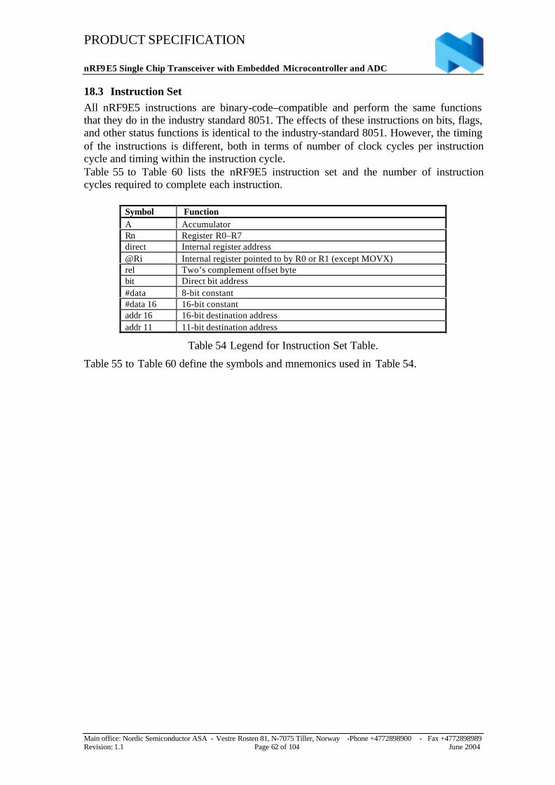
PRODUCT SPECIFICATION
nRF9E5 Single Chip Transceiver with Embedded Microcontroller and ADC
Main office: Nordic Semiconductor ASA - Vestre Rosten 81, N-7075 Tiller, Norway -Phone +4772898900 - Fax +4772898989Revision: 1.1 Page 62 of 104 June 2004
18.3 Instruction SetAll nRF9E5 instructions are binary-code–compatible and perform the same functionsthat they do in the industry standard 8051. The effects of these instructions on bits, flags,and other status functions is identical to the industry-standard 8051. However, the timingof the instructions is different, both in terms of number of clock cycles per instructioncycle and timing within the instruction cycle.Table 55 to Table 60 lists the nRF9E5 instruction set and the number of instructioncycles required to complete each instruction.
Symbol FunctionA AccumulatorRn Register R0–R7direct Internal register address@Ri Internal register pointed to by R0 or R1 (except MOVX)rel Two’s complement offset bytebit Direct bit address#data 8-bit constant#data 16 16-bit constantaddr 16 16-bit destination addressaddr 11 11-bit destination address
Table 54 Legend for Instruction Set Table.
Table 55 to Table 60 define the symbols and mnemonics used in Table 54.
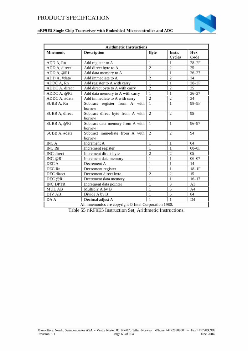
PRODUCT SPECIFICATION
nRF9E5 Single Chip Transceiver with Embedded Microcontroller and ADC
Main office: Nordic Semiconductor ASA - Vestre Rosten 81, N-7075 Tiller, Norway -Phone +4772898900 - Fax +4772898989Revision: 1.1 Page 63 of 104 June 2004
Arithmetic InstructionsMnemonic Description Byte Instr.
CyclesHexCode
ADD A, Rn Add register to A 1 1 28–2FADD A, direct Add direct byte to A 2 2 25ADD A, @Ri Add data memory to A 1 1 26–27ADD A, #data Add immediate to A 2 2 24ADDC A, Rn Add register to A with carry 1 1 38–3FADDC A, direct Add direct byte to A with carry 2 2 35ADDC A, @Ri Add data memory to A with carry 1 1 36–37ADDC A, #data Add immediate to A with carry 2 2 34SUBB A, Rn Subtract register from A with
borrow1 1 98–9F
SUBB A, direct Subtract direct byte from A withborrow
2 2 95
SUBB A, @Ri Subtract data memory from A withborrow
1 1 96–97
SUBB A, #data Subtract immediate from A withborrow
2 2 94
INC A Increment A 1 1 04INC Rn Increment register 1 1 08–0FINC direct Increment direct byte 2 2 05INC @Ri Increment data memory 1 1 06–07DEC A Decrement A 1 1 14DEC Rn Decrement register 1 1 18–1FDEC direct Decrement direct byte 2 2 15DEC @Ri Decrement data memory 1 1 16–17INC DPTR Increment data pointer 1 3 A3MUL AB Multiply A by B 1 5 A4DIV AB Divide A by B 1 5 84DA A Decimal adjust A 1 1 D4
All mnemonics are copyright © Intel Corporation 1980.Table 55 nRF9E5 Instruction Set, Arithmetic Instructions.
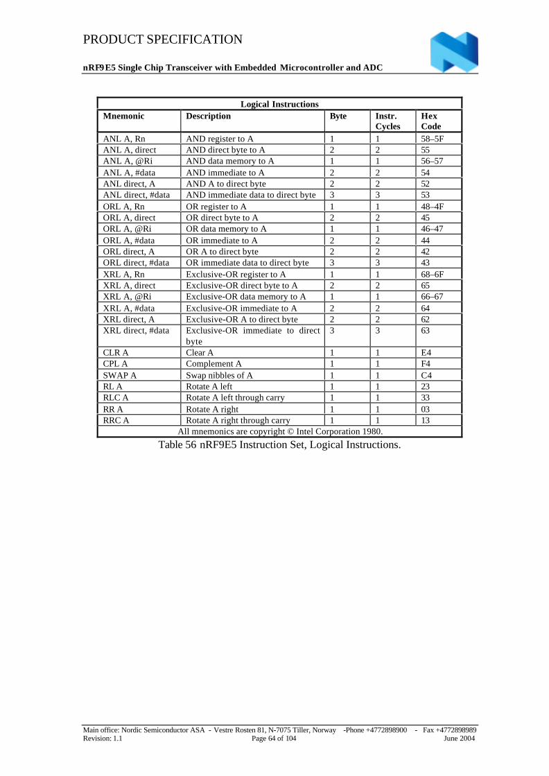
PRODUCT SPECIFICATION
nRF9E5 Single Chip Transceiver with Embedded Microcontroller and ADC
Main office: Nordic Semiconductor ASA - Vestre Rosten 81, N-7075 Tiller, Norway -Phone +4772898900 - Fax +4772898989Revision: 1.1 Page 64 of 104 June 2004
Logical InstructionsMnemonic Description Byte Instr.
CyclesHexCode
ANL A, Rn AND register to A 1 1 58–5FANL A, direct AND direct byte to A 2 2 55ANL A, @Ri AND data memory to A 1 1 56–57ANL A, #data AND immediate to A 2 2 54ANL direct, A AND A to direct byte 2 2 52ANL direct, #data AND immediate data to direct byte 3 3 53ORL A, Rn OR register to A 1 1 48–4FORL A, direct OR direct byte to A 2 2 45ORL A, @Ri OR data memory to A 1 1 46–47ORL A, #data OR immediate to A 2 2 44ORL direct, A OR A to direct byte 2 2 42ORL direct, #data OR immediate data to direct byte 3 3 43XRL A, Rn Exclusive-OR register to A 1 1 68–6FXRL A, direct Exclusive-OR direct byte to A 2 2 65XRL A, @Ri Exclusive-OR data memory to A 1 1 66–67XRL A, #data Exclusive-OR immediate to A 2 2 64XRL direct, A Exclusive-OR A to direct byte 2 2 62XRL direct, #data Exclusive-OR immediate to direct
byte3 3 63
CLR A Clear A 1 1 E4CPL A Complement A 1 1 F4SWAP A Swap nibbles of A 1 1 C4RL A Rotate A left 1 1 23RLC A Rotate A left through carry 1 1 33RR A Rotate A right 1 1 03RRC A Rotate A right through carry 1 1 13
All mnemonics are copyright © Intel Corporation 1980.
Table 56 nRF9E5 Instruction Set, Logical Instructions.
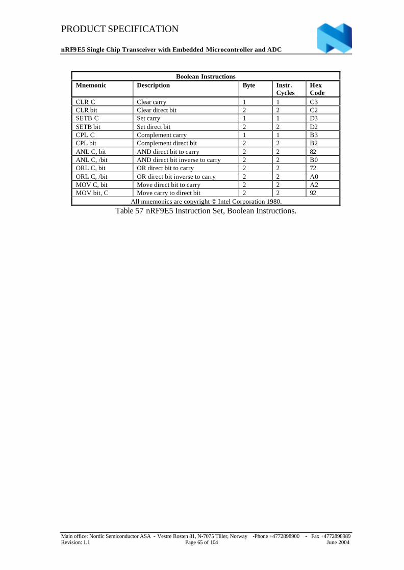
PRODUCT SPECIFICATION
nRF9E5 Single Chip Transceiver with Embedded Microcontroller and ADC
Main office: Nordic Semiconductor ASA - Vestre Rosten 81, N-7075 Tiller, Norway -Phone +4772898900 - Fax +4772898989Revision: 1.1 Page 65 of 104 June 2004
Boolean InstructionsMnemonic Description Byte Instr.
CyclesHexCode
CLR C Clear carry 1 1 C3CLR bit Clear direct bit 2 2 C2SETB C Set carry 1 1 D3SETB bit Set direct bit 2 2 D2CPL C Complement carry 1 1 B3CPL bit Complement direct bit 2 2 B2ANL C, bit AND direct bit to carry 2 2 82ANL C, /bit AND direct bit inverse to carry 2 2 B0ORL C, bit OR direct bit to carry 2 2 72ORL C, /bit OR direct bit inverse to carry 2 2 A0MOV C, bit Move direct bit to carry 2 2 A2MOV bit, C Move carry to direct bit 2 2 92
All mnemonics are copyright © Intel Corporation 1980.Table 57 nRF9E5 Instruction Set, Boolean Instructions.
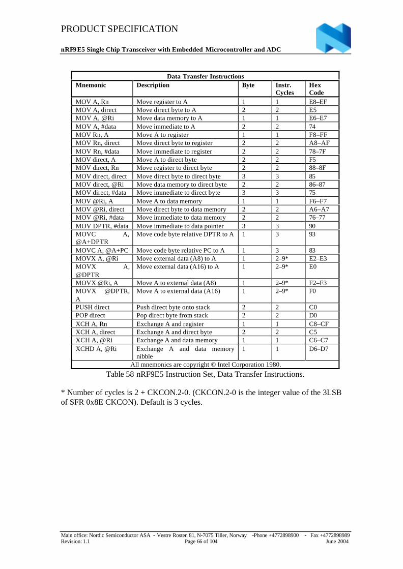
PRODUCT SPECIFICATION
nRF9E5 Single Chip Transceiver with Embedded Microcontroller and ADC
Main office: Nordic Semiconductor ASA - Vestre Rosten 81, N-7075 Tiller, Norway -Phone +4772898900 - Fax +4772898989Revision: 1.1 Page 66 of 104 June 2004
Data Transfer InstructionsMnemonic Description Byte Instr.
CyclesHexCode
MOV A, Rn Move register to A 1 1 E8–EFMOV A, direct Move direct byte to A 2 2 E5MOV A, @Ri Move data memory to A 1 1 E6–E7MOV A, #data Move immediate to A 2 2 74MOV Rn, A Move A to register 1 1 F8–FFMOV Rn, direct Move direct byte to register 2 2 A8–AFMOV Rn, #data Move immediate to register 2 2 78–7FMOV direct, A Move A to direct byte 2 2 F5MOV direct, Rn Move register to direct byte 2 2 88–8FMOV direct, direct Move direct byte to direct byte 3 3 85MOV direct, @Ri Move data memory to direct byte 2 2 86–87MOV direct, #data Move immediate to direct byte 3 3 75MOV @Ri, A Move A to data memory 1 1 F6–F7MOV @Ri, direct Move direct byte to data memory 2 2 A6–A7MOV @Ri, #data Move immediate to data memory 2 2 76–77MOV DPTR, #data Move immediate to data pointer 3 3 90MOVC A,@A+DPTR
Move code byte relative DPTR to A 1 3 93
MOVC A, @A+PC Move code byte relative PC to A 1 3 83MOVX A, @Ri Move external data (A8) to A 1 2–9* E2–E3MOVX A,@DPTR
Move external data (A16) to A 1 2–9* E0
MOVX @Ri, A Move A to external data (A8) 1 2–9* F2–F3MOVX @DPTR,A
Move A to external data (A16) 1 2–9* F0
PUSH direct Push direct byte onto stack 2 2 C0POP direct Pop direct byte from stack 2 2 D0XCH A, Rn Exchange A and register 1 1 C8–CFXCH A, direct Exchange A and direct byte 2 2 C5XCH A, @Ri Exchange A and data memory 1 1 C6–C7XCHD A, @Ri Exchange A and data memory
nibble1 1 D6–D7
All mnemonics are copyright © Intel Corporation 1980.
Table 58 nRF9E5 Instruction Set, Data Transfer Instructions.
* Number of cycles is 2 + CKCON.2-0. (CKCON.2-0 is the integer value of the 3LSBof SFR 0x8E CKCON). Default is 3 cycles.
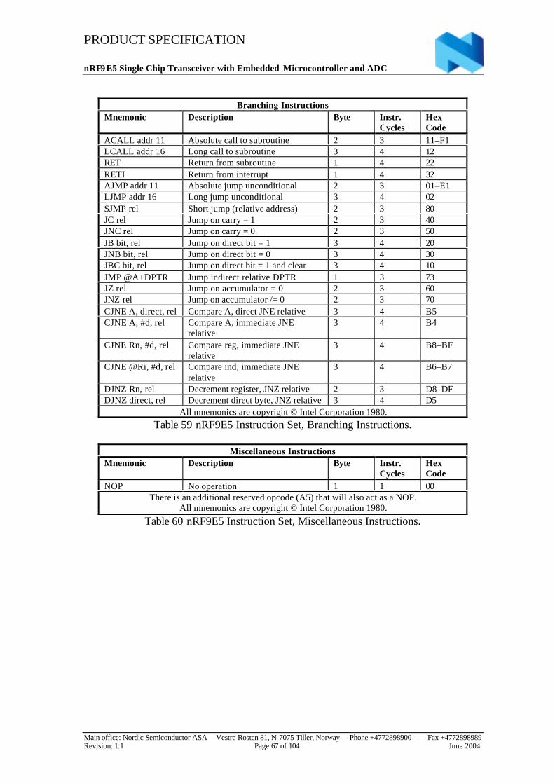
PRODUCT SPECIFICATION
nRF9E5 Single Chip Transceiver with Embedded Microcontroller and ADC
Main office: Nordic Semiconductor ASA - Vestre Rosten 81, N-7075 Tiller, Norway -Phone +4772898900 - Fax +4772898989Revision: 1.1 Page 67 of 104 June 2004
Branching InstructionsMnemonic Description Byte Instr.
CyclesHexCode
ACALL addr 11 Absolute call to subroutine 2 3 11–F1LCALL addr 16 Long call to subroutine 3 4 12RET Return from subroutine 1 4 22RETI Return from interrupt 1 4 32AJMP addr 11 Absolute jump unconditional 2 3 01–E1LJMP addr 16 Long jump unconditional 3 4 02SJMP rel Short jump (relative address) 2 3 80JC rel Jump on carry = 1 2 3 40JNC rel Jump on carry = 0 2 3 50JB bit, rel Jump on direct bit = 1 3 4 20JNB bit, rel Jump on direct bit = 0 3 4 30JBC bit, rel Jump on direct bit = 1 and clear 3 4 10JMP @A+DPTR Jump indirect relative DPTR 1 3 73JZ rel Jump on accumulator = 0 2 3 60JNZ rel Jump on accumulator /= 0 2 3 70CJNE A, direct, rel Compare A, direct JNE relative 3 4 B5CJNE A, #d, rel Compare A, immediate JNE
relative3 4 B4
CJNE Rn, #d, rel Compare reg, immediate JNErelative
3 4 B8–BF
CJNE @Ri, #d, rel Compare ind, immediate JNErelative
3 4 B6–B7
DJNZ Rn, rel Decrement register, JNZ relative 2 3 D8–DFDJNZ direct, rel Decrement direct byte, JNZ relative 3 4 D5
All mnemonics are copyright © Intel Corporation 1980.Table 59 nRF9E5 Instruction Set, Branching Instructions.
Miscellaneous InstructionsMnemonic Description Byte Instr.
CyclesHexCode
NOP No operation 1 1 00There is an additional reserved opcode (A5) that will also act as a NOP.
All mnemonics are copyright © Intel Corporation 1980.
Table 60 nRF9E5 Instruction Set, Miscellaneous Instructions.
PRODUCT SPECIFICATION
nRF9E5 Single Chip Transceiver with Embedded Microcontroller and ADC
Main office: Nordic Semiconductor ASA - Vestre Rosten 81, N-7075 Tiller, Norway -Phone +4772898900 - Fax +4772898989Revision: 1.1 Page 68 of 104 June 2004
18.4 Instruction TimingInstruction cycles in the nRF9E5 are four clock cycles in length, as opposed to twelveclock cycles per instruction cycle in the standard 8051. This translates to a 3Ximprovement in execution time for most instructions. However, some instructionsrequire a different number of instruction cycles on the nRF9E5 than they do on thestandard 8051. In the standard 8051, all instructions except for MUL and DIV take oneor two instruction cycles to complete. In the nRF9E5 architecture, instructions can takebetween one and five instruction cycles to complete. For example, in the standard 8051,the instructions MOVX A, @DPTR and MOV direct, direct each take two instructioncycles (twenty-four clock cycles) to execute. In the nRF9E5 architecture, MOVX A,@DPTR takes two instruction cycles (eight clock cycles) and MOV direct, direct takesthree instruction cycles (twelve clock cycles). Both instructions execute faster on thenRF9E5 than they do on the standard 8051, but require different numbers of clockcycles.For timing of real-time events, use the numbers of instruction cycles from Table 55 toTable 60 to calculate the timing of software loops. The bytes column of these tableindicates the number of memory accesses (bytes) needed to execute the instruction. Inmost cases, the number of bytes is equal to the number of instruction cycles required tocomplete the instruction. However, as indicated in Table 55, there are some instructions(for example, DIV and MUL) that require a greater number of instruction cycles thanmemory accesses.By default, the nRF9E5 timer/counters run at twelve clock cycles perincrement so that timer-based events have the same timing as with the standard 8051.The timers can be configured to run at four clock cycles per increment to take advantageof the higher speed of the nRF9E5.
18.5 Dual Data PointersThe nRF9E5 employs dual data pointers to accelerate data memory block moves. Thestandard 8051 data pointer (DPTR) is a 16-bit value used to address external data RAMor peripherals. The nRF9E5 maintains the standard data pointer as DPTR0 at SFRlocations 0x82 and 0x83. It is not necessary to modify code to use DPTR0. The nRF9E5adds a second data pointer (DPTR1) at SFR locations 0x84 and 0x85. The SEL bit in theDPTR Select register, DPS (SFR 0x86), selects the active pointer. When SEL = 0,instructions that use the DPTR will use DPL0 and DPH0. When SEL = 1, instructionsthat use the DPTR will use DPL1 and DPH1. SEL is the bit 0 of SFR location 0x86. Noother bits of SFR location 0x86 are used. All DPTR-related instructions use thecurrently selected data pointer. To switch the active pointer, toggle the SEL bit. Thefastest way to do so is to use the increment instruction (INC DPS). This requires onlyone instruction to switch from a source address to a destination address, savingapplication code from having to save source and destination addresses when doing ablock move. Using dual data pointers provides significantly increased efficiency whenmoving large blocks of data.The SFR locations related to the dual data pointers are: - 0x82 DPL0 DPTR0 low byte - 0x83 DPH0 DPTR0 high byte - 0x84 DPL1 DPTR1 low byte - 0x85 DPH1 DPTR1 high byte - 0x86 DPS DPTR Select (LSB)
PRODUCT SPECIFICATION
nRF9E5 Single Chip Transceiver with Embedded Microcontroller and ADC
Main office: Nordic Semiconductor ASA - Vestre Rosten 81, N-7075 Tiller, Norway -Phone +4772898900 - Fax +4772898989Revision: 1.1 Page 69 of 104 June 2004
18.6 Special Function RegistersThe Special Function Registers (SFRs) control several of the features of the nRF9E5.Most of the nRF9E5 SFRs are identical to the standard 8051 SFRs. However, there areadditional SFRs that control features that are not available in the standard 8051. Table61 lists the nRF9E5 SFRs and indicates which SFRs are not included in the standard8051 SFR space. When writing software for the nRF9E5, use equate statements todefine the SFRs that are specific to the nRF9E5 and custom peripherals. In Table 61,SFR bit positions that contain a 0 or a 1 cannot be written to and, when read, alwaysreturn the value shown (0 or 1). SFR bit positions that contain “–” are available but notused. Table 62 shows the value of each SFR, after power-on reset or a watchdog reset,together with a pointer to a detailled description of each register. Please note that anyunused address in the SFR address space is reserved and should not be written to.
Notes to Table 61 on next page :(1) Not part of standard 8051 architecture.(2) Registers unique to nRF9E5(3) P0, P1 and P3 differ from standard 8051
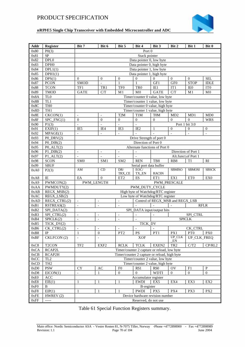
PRODUCT SPECIFICATION
nRF9E5 Single Chip Transceiver with Embedded Microcontroller and ADC
Main office: Nordic Semiconductor ASA - Vestre Rosten 81, N-7075 Tiller, Norway -Phone +4772898900 - Fax +4772898989Revision: 1.1 Page 70 of 104 June 2004
Addr Register Bit 7 Bit 6 Bit 5 Bit 4 Bit 3 Bit 2 Bit 1 Bit 00x80 P0(3) Port 00x81 SP Stack pointer0x82 DPL0 Data pointer 0, low byte0x83 DPH0 Data pointer 0, high byte0x84 DPL1(1) Data pointer 1, low byte0x85 DPH1(1) Data pointer 1, high byte0x86 DPS(1) 0 0 0 0 0 0 0 SEL0x87 PCON SMOD 1 1 GF1 GF0 STOP IDLE0x88 TCON TF1 TR1 TF0 TR0 IE1 IT1 IE0 IT00x89 TMOD GATE C/T M1 M0 GATE C/T M1 M00x8A TL0 Timer/counter 0 value, low byte0x8B TL1 Timer/counter 1 value, low byte0x8C TH0 Timer/counter 0 value, high byte0x8D TH1 Timer/counter 1 value, high byte0x8E CKCON(1) T2M T1M T0M MD2 MD1 MD00x8F SPC_FNC(1) 0 0 0 0 0 0 0 WRS0x90 P1(3) Port 1 bit 3:00x91 EXIF(1) IE5 IE4 IE3 IE2 1 0 0 00x92 MPAGE(1) 0x93 P0_DRV(2) Drive Strength of port 00x94 P0_DIR(2) Direction of Port 00x95 P0_ALT(2) Alternate functions of Port 00x96 P1_DIR(2) Direction of Port 10x97 P1_ALT(2) Alt.funct.of Port 10x98 SCON SM0 SM1 SM2 REN TB8 RB8 TI RI0x99 SBUF Serial port data buffer0xA0 P2(3) AM CD DR/
TRX_CEEOC/TX_EN RACSN
SBMISO SBMOSI SBSCK
0xA8 IE EA 0 ET2 ES ET1 EX1 ET0 EX00xA9 PWMCON(2) PWM_LENGTH PWM_PRESCALE0xAA PWMDUTY(2) PWM_DUTY_CYCLE0xAB REGX_MSB(2) High byte of Watchdog/RTC register0xAC REGX_LSB(2) Low byte of Watchdog/RTC register0xAD REGX_CTRL(2) Control of REGX_MSB and REGX_LSB0xB1 RSTREAS(2) RFLR0xB2 SPI_DATA(2) SPI_DATA input/output bits0xB3 SPI_CTRL(2) SPI_CTRL0xB4 SPICLK(2) SPICLK0xB5 TICK_DV(2) TICK_DV0xB6 CK_CTRL(2) CK_CTRL0xB8 IP 1 0 PT2 PS PT1 PX1 PT0 PX00xBF CKLFCON (2) - - XOF UP_CLK
_ENUP_CLK_FREQ
0xC8 T2CON TF2 EXF2 RCLK TCLK EXEN2 TR2 C/T2 CP/RL20xCA RCAP2L Timer/counter 2 capture or reload, low byte0xCB RCAP2H Timer/counter 2 capture or reload, high byte0xCC TL2 Timer/counter 2 value, low byte0xCD TH2 Timer/counter 2 value, high byte0xD0 PSW CY AC F0 RS1 RS0 OV F1 P0xD8 EICON(1) - 1 0 0 WDTI 0 0 00xE0 ACC Accumulator register0xE8 EIE(1) 1 1 1 EWDI EX5 EX4 EX3 EX20xF0 B B-register0xF8 EIP(1) 1 1 1 PWDI PX5 PX4 PX3 PX20xFE HWREV (2) Device hardware revision number0xFF ----- Reserved, do not use
Table 61 Special Function Registers summary.
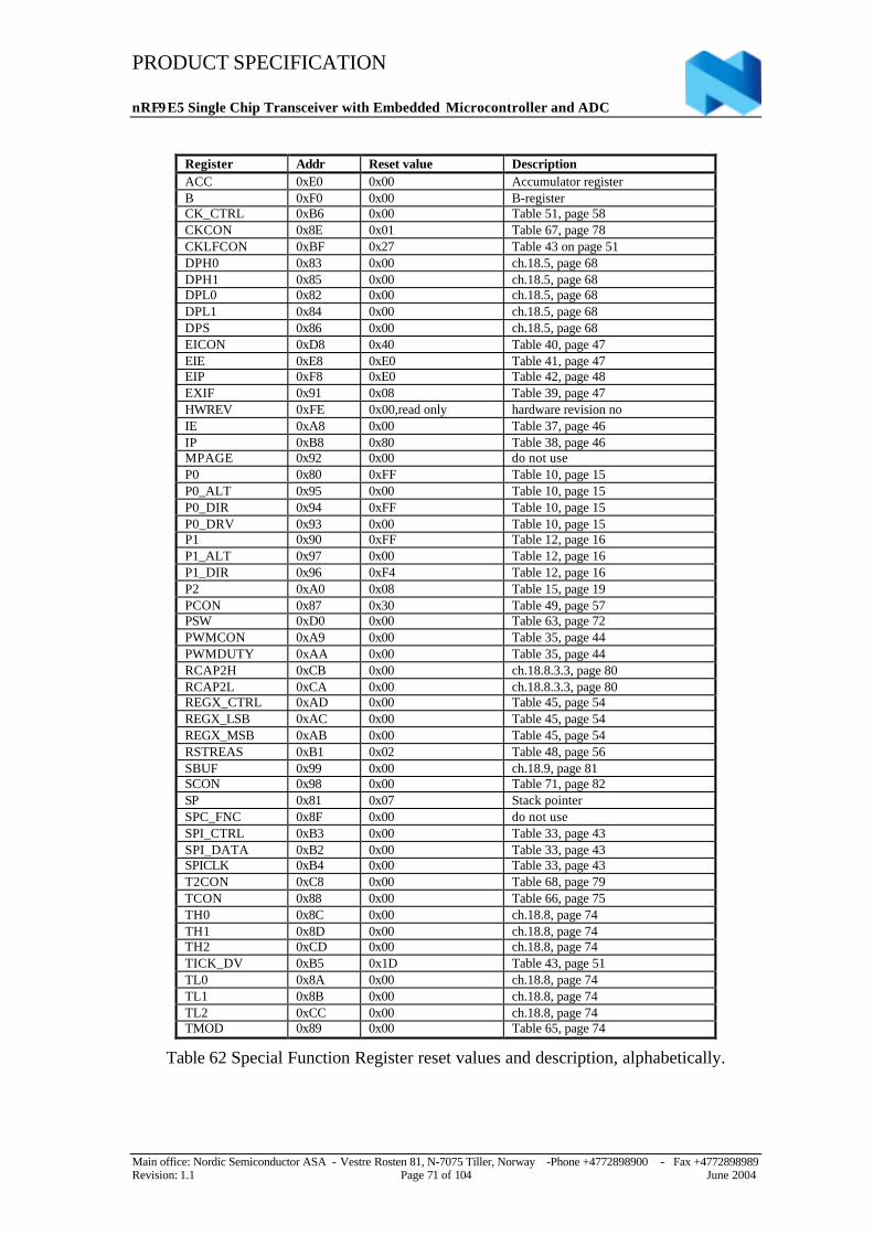
PRODUCT SPECIFICATION
nRF9E5 Single Chip Transceiver with Embedded Microcontroller and ADC
Main office: Nordic Semiconductor ASA - Vestre Rosten 81, N-7075 Tiller, Norway -Phone +4772898900 - Fax +4772898989Revision: 1.1 Page 71 of 104 June 2004
Register Addr Reset value DescriptionACC 0xE0 0x00 Accumulator registerB 0xF0 0x00 B-registerCK_CTRL 0xB6 0x00 Table 51, page 58CKCON 0x8E 0x01 Table 67, page 78CKLFCON 0xBF 0x27 Table 43 on page 51DPH0 0x83 0x00 ch.18.5, page 68DPH1 0x85 0x00 ch.18.5, page 68DPL0 0x82 0x00 ch.18.5, page 68DPL1 0x84 0x00 ch.18.5, page 68DPS 0x86 0x00 ch.18.5, page 68EICON 0xD8 0x40 Table 40, page 47EIE 0xE8 0xE0 Table 41, page 47EIP 0xF8 0xE0 Table 42, page 48EXIF 0x91 0x08 Table 39, page 47HWREV 0xFE 0x00,read only hardware revision noIE 0xA8 0x00 Table 37, page 46IP 0xB8 0x80 Table 38, page 46MPAGE 0x92 0x00 do not useP0 0x80 0xFF Table 10, page 15P0_ALT 0x95 0x00 Table 10, page 15P0_DIR 0x94 0xFF Table 10, page 15P0_DRV 0x93 0x00 Table 10, page 15P1 0x90 0xFF Table 12, page 16P1_ALT 0x97 0x00 Table 12, page 16P1_DIR 0x96 0xF4 Table 12, page 16P2 0xA0 0x08 Table 15, page 19PCON 0x87 0x30 Table 49, page 57PSW 0xD0 0x00 Table 63, page 72PWMCON 0xA9 0x00 Table 35, page 44PWMDUTY 0xAA 0x00 Table 35, page 44RCAP2H 0xCB 0x00 ch.18.8.3.3, page 80RCAP2L 0xCA 0x00 ch.18.8.3.3, page 80REGX_CTRL 0xAD 0x00 Table 45, page 54REGX_LSB 0xAC 0x00 Table 45, page 54REGX_MSB 0xAB 0x00 Table 45, page 54RSTREAS 0xB1 0x02 Table 48, page 56SBUF 0x99 0x00 ch.18.9, page 81SCON 0x98 0x00 Table 71, page 82SP 0x81 0x07 Stack pointerSPC_FNC 0x8F 0x00 do not useSPI_CTRL 0xB3 0x00 Table 33, page 43SPI_DATA 0xB2 0x00 Table 33, page 43SPICLK 0xB4 0x00 Table 33, page 43T2CON 0xC8 0x00 Table 68, page 79TCON 0x88 0x00 Table 66, page 75TH0 0x8C 0x00 ch.18.8, page 74TH1 0x8D 0x00 ch.18.8, page 74TH2 0xCD 0x00 ch.18.8, page 74TICK_DV 0xB5 0x1D Table 43, page 51TL0 0x8A 0x00 ch.18.8, page 74TL1 0x8B 0x00 ch.18.8, page 74TL2 0xCC 0x00 ch.18.8, page 74TMOD 0x89 0x00 Table 65, page 74
Table 62 Special Function Register reset values and description, alphabetically.
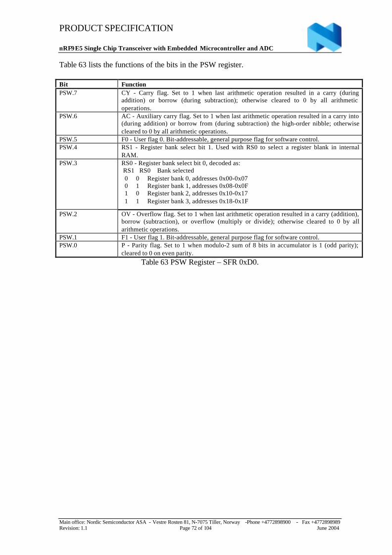
PRODUCT SPECIFICATION
nRF9E5 Single Chip Transceiver with Embedded Microcontroller and ADC
Main office: Nordic Semiconductor ASA - Vestre Rosten 81, N-7075 Tiller, Norway -Phone +4772898900 - Fax +4772898989Revision: 1.1 Page 72 of 104 June 2004
Table 63 lists the functions of the bits in the PSW register.
Bit FunctionPSW.7 CY Carry flag. Set to 1 when last arithmetic operation resulted in a carry (during
addition) or borrow (during subtraction); otherwise cleared to 0 by all arithmeticoperations.
PSW.6 AC Auxiliary carry flag. Set to 1 when last arithmetic operation resulted in a carry into(during addition) or borrow from (during subtraction) the high-order nibble; otherwisecleared to 0 by all arithmetic operations.
PSW.5 F0 User flag 0. Bit-addressable, general purpose flag for software control.PSW.4 RS1 Register bank select bit 1. Used with RS0 to select a register blank in internal
RAM.PSW.3 RS0 Register bank select bit 0, decoded as:
RS1 RS0 Bank selected 0 0 Register bank 0, addresses 0x000x07 0 1 Register bank 1, addresses 0x080x0F 1 0 Register bank 2, addresses 0x100x17 1 1 Register bank 3, addresses 0x180x1F
PSW.2 OV Overflow flag. Set to 1 when last arithmetic operation resulted in a carry (addition),borrow (subtraction), or overflow (multiply or divide); otherwise cleared to 0 by allarithmetic operations.
PSW.1 F1 User flag 1. Bit-addressable, general purpose flag for software control.PSW.0 P Parity flag. Set to 1 when modulo-2 sum of 8 bits in accumulator is 1 (odd parity);
cleared to 0 on even parity.Table 63 PSW Register – SFR 0xD0.
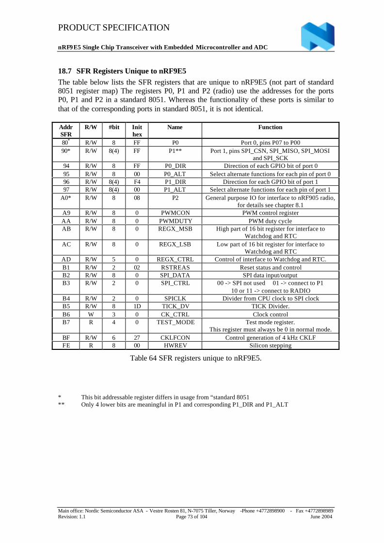
PRODUCT SPECIFICATION
nRF9E5 Single Chip Transceiver with Embedded Microcontroller and ADC
Main office: Nordic Semiconductor ASA - Vestre Rosten 81, N-7075 Tiller, Norway -Phone +4772898900 - Fax +4772898989Revision: 1.1 Page 73 of 104 June 2004
18.7 SFR Registers Unique to nRF9E5The table below lists the SFR registers that are unique to nRF9E5 (not part of standard8051 register map) The registers P0, P1 and P2 (radio) use the addresses for the portsP0, P1 and P2 in a standard 8051. Whereas the functionality of these ports is similar tothat of the corresponding ports in standard 8051, it is not identical.
AddrSFR
R/W #bit Inithex
Name Function
80* R/W 8 FF P0 Port 0, pins P07 to P0090* R/W 8(4) FF P1** Port 1, pins SPI_CSN, SPI_MISO, SPI_MOSI
and SPI_SCK94 R/W 8 FF P0_DIR Direction of each GPIO bit of port 095 R/W 8 00 P0_ALT Select alternate functions for each pin of port 096 R/W 8(4) F4 P1_DIR Direction for each GPIO bit of port 197 R/W 8(4) 00 P1_ALT Select alternate functions for each pin of port 1
A0* R/W 8 08 P2 General purpose IO for interface to nRF905 radio,for details see chapter 8.1
A9 R/W 8 0 PWMCON PWM control registerAA R/W 8 0 PWMDUTY PWM duty cycleAB R/W 8 0 REGX_MSB High part of 16 bit register for interface to
Watchdog and RTCAC R/W 8 0 REGX_LSB Low part of 16 bit register for interface to
Watchdog and RTCAD R/W 5 0 REGX_CTRL Control of interface to Watchdog and RTC.B1 R/W 2 02 RSTREAS Reset status and controlB2 R/W 8 0 SPI_DATA SPI data input/outputB3 R/W 2 0 SPI_CTRL 00 -> SPI not used 01 -> connect to P1
10 or 11 -> connect to RADIOB4 R/W 2 0 SPICLK Divider from CPU clock to SPI clockB5 R/W 8 1D TICK_DV TICK Divider.B6 W 3 0 CK_CTRL Clock controlB7 R 4 0 TEST_MODE Test mode register.
This register must always be 0 in normal mode.BF R/W 6 27 CKLFCON Control generation of 4 kHz CKLFFE R 8 00 HWREV Silicon stepping
Table 64 SFR registers unique to nRF9E5.
* This bit addressable register differs in usage from “standard 8051** Only 4 lower bits are meaningful in P1 and corresponding P1_DIR and P1_ALT
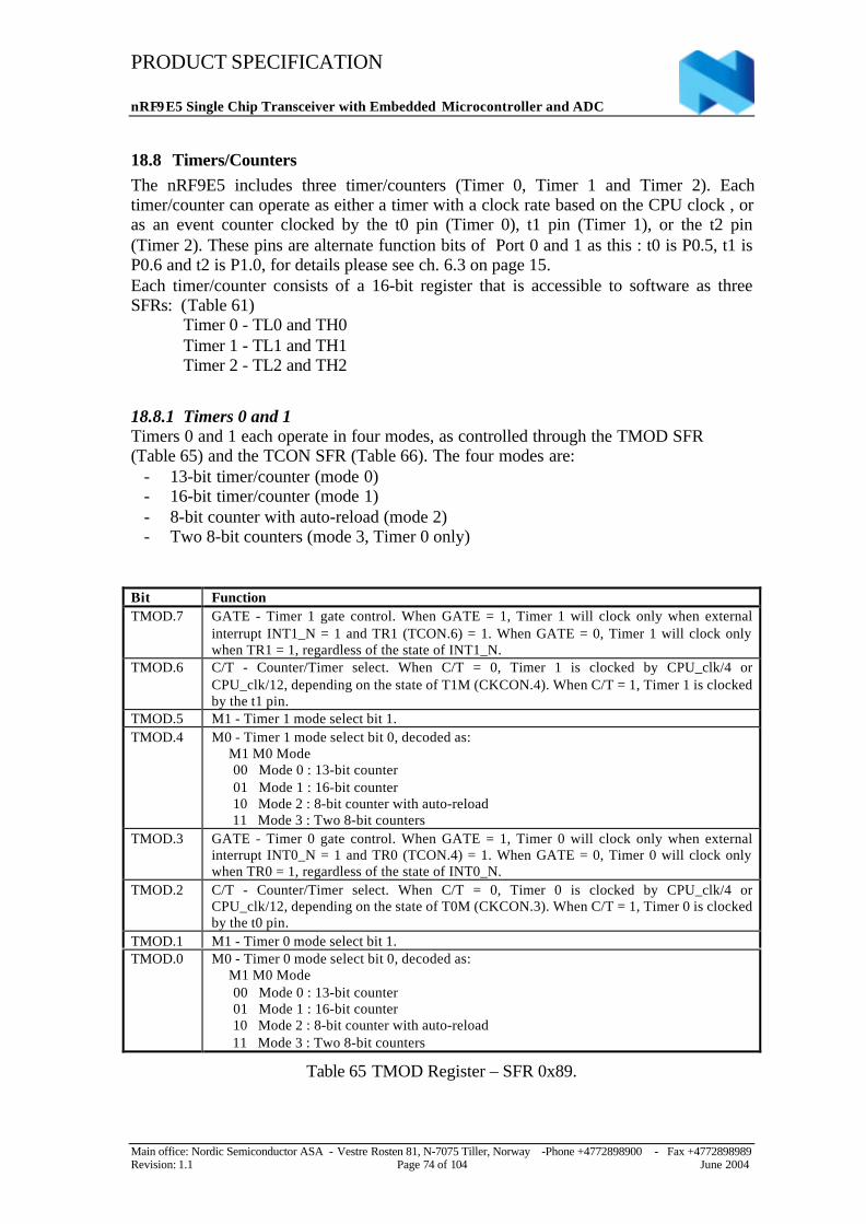
PRODUCT SPECIFICATION
nRF9E5 Single Chip Transceiver with Embedded Microcontroller and ADC
Main office: Nordic Semiconductor ASA - Vestre Rosten 81, N-7075 Tiller, Norway -Phone +4772898900 - Fax +4772898989Revision: 1.1 Page 74 of 104 June 2004
18.8 Timers/CountersThe nRF9E5 includes three timer/counters (Timer 0, Timer 1 and Timer 2). Eachtimer/counter can operate as either a timer with a clock rate based on the CPU clock , oras an event counter clocked by the t0 pin (Timer 0), t1 pin (Timer 1), or the t2 pin(Timer 2). These pins are alternate function bits of Port 0 and 1 as this : t0 is P0.5, t1 isP0.6 and t2 is P1.0, for details please see ch. 6.3 on page 15.Each timer/counter consists of a 16-bit register that is accessible to software as threeSFRs: (Table 61)
Timer 0 TL0 and TH0Timer 1 TL1 and TH1Timer 2 TL2 and TH2
18.8.1 Timers 0 and 1Timers 0 and 1 each operate in four modes, as controlled through the TMOD SFR(Table 65) and the TCON SFR (Table 66). The four modes are:
- 13-bit timer/counter (mode 0)- 16-bit timer/counter (mode 1)- 8-bit counter with auto-reload (mode 2)- Two 8-bit counters (mode 3, Timer 0 only)
Bit FunctionTMOD.7 GATE Timer 1 gate control. When GATE = 1, Timer 1 will clock only when external
interrupt INT1_N = 1 and TR1 (TCON.6) = 1. When GATE = 0, Timer 1 will clock onlywhen TR1 = 1, regardless of the state of INT1_N.
TMOD.6 C/T Counter/Timer select. When C/T = 0, Timer 1 is clocked by CPU_clk/4 orCPU_clk/12, depending on the state of T1M (CKCON.4). When C/T = 1, Timer 1 is clockedby the t1 pin.
TMOD.5 M1 Timer 1 mode select bit 1.TMOD.4 M0 Timer 1 mode select bit 0, decoded as:
M1 M0 Mode 00 Mode 0 : 13-bit counter 01 Mode 1 : 16-bit counter 10 Mode 2 : 8-bit counter with auto-reload 11 Mode 3 : Two 8-bit counters
TMOD.3 GATE Timer 0 gate control. When GATE = 1, Timer 0 will clock only when externalinterrupt INT0_N = 1 and TR0 (TCON.4) = 1. When GATE = 0, Timer 0 will clock onlywhen TR0 = 1, regardless of the state of INT0_N.
TMOD.2 C/T Counter/Timer select. When C/T = 0, Timer 0 is clocked by CPU_clk/4 orCPU_clk/12, depending on the state of T0M (CKCON.3). When C/T = 1, Timer 0 is clockedby the t0 pin.
TMOD.1 M1 Timer 0 mode select bit 1.TMOD.0 M0 Timer 0 mode select bit 0, decoded as:
M1 M0 Mode 00 Mode 0 : 13-bit counter 01 Mode 1 : 16-bit counter 10 Mode 2 : 8-bit counter with auto-reload 11 Mode 3 : Two 8-bit counters
Table 65 TMOD Register – SFR 0x89.
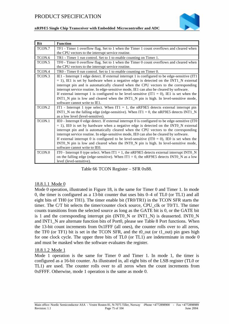
PRODUCT SPECIFICATION
nRF9E5 Single Chip Transceiver with Embedded Microcontroller and ADC
Main office: Nordic Semiconductor ASA - Vestre Rosten 81, N-7075 Tiller, Norway -Phone +4772898900 - Fax +4772898989Revision: 1.1 Page 75 of 104 June 2004
Bit FunctionTCON.7 TF1 Timer 1 overflow flag. Set to 1 when the Timer 1 count overflows and cleared when
the CPU vectors to the interrupt service routine.TCON.6 TR1 Timer 1 run control. Set to 1 to enable counting on Timer 1.TCON.5 TF0 Timer 0 overflow flag. Set to 1 when the Timer 0 count overflows and cleared when
the CPU vectors to the interrupt service routine.TCON.4 TR0 Timer 0 run control. Set to 1 to enable counting on Timer 0.TCON.3 IE1 Interrupt 1 edge detect. If external interrupt 1 is configured to be edge-sensitive (IT1
= 1), IE1 is set by hardware when a negative edge is detected on the INT1_N externalinterrupt pin and is automatically cleared when the CPU vectors to the correspondinginterrupt service routine. In edge-sensitive mode, IE1 can also be cleared by software.If external interrupt 1 is configured to be level-sensitive (IT1 = 0), IE1 is set when theINT1_N pin is low and cleared when the INT1_N pin is high. In level-sensitive mode,software cannot write to IE1.
TCON.2 IT1 Interrupt 1 type select. When IT1 = 1, the nRF9E5 detects external interrupt pinINT1_N on the falling edge (edge-sensitive). When IT1 = 0, the nRF9E5 detects INT1_Nas a low level (level-sensitive).
TCON.1 IE0 Interrupt 0 edge detect. If external interrupt 0 is configured to be edge-sensitive (IT0= 1), IE0 is set by hardware when a negative edge is detected on the INT0_N externalinterrupt pin and is automatically cleared when the CPU vectors to the correspondinginterrupt service routine. In edge-sensitive mode, IE0 can also be cleared by software.If external interrupt 0 is configured to be level-sensitive (IT0 = 0), IE0 is set when theINT0_N pin is low and cleared when the INT0_N pin is high. In level-sensitive mode,software cannot write to IE0.
TCON.0 IT0 Interrupt 0 type select. When IT1 = 1, the nRF9E5 detects external interrupt INT0_Non the falling edge (edge-sensitive). When IT1 = 0, the nRF9E5 detects INT0_N as a lowlevel (level-sensitive).
Table 66 TCON Register – SFR 0x88.
18.8.1.1 Mode 0Mode 0 operation, illustrated in Figure 18, is the same for Timer 0 and Timer 1. In mode0, the timer is configured as a 13-bit counter that uses bits 0–4 of TL0 (or TL1) and alleight bits of TH0 (or TH1). The timer enable bit (TR0/TR1) in the TCON SFR starts thetimer. The C/T bit selects the timer/counter clock source, CPU_clk or T0/T1. The timercounts transitions from the selected source as long as the GATE bit is 0, or the GATE bitis 1 and the corresponding interrupt pin (INT0_N or INT1_N) is deasserted. INT0_Nand INT1_N are alternate function bits of Port0, please see Table 8 Port functions. Whenthe 13-bit count increments from 0x1FFF (all ones), the counter rolls over to all zeros,the TF0 (or TF1) bit is set in the TCON SFR, and the t0_out (or t1_out) pin goes highfor one clock cycle. The upper three bits of TL0 (or TL1) are indeterminate in mode 0and must be masked when the software evaluates the register.
18.8.1.2 Mode 1Mode 1 operation is the same for Timer 0 and Timer 1. In mode 1, the timer isconfigured as a 16-bit counter. As illustrated in, all eight bits of the LSB register (TL0 orTL1) are used. The counter rolls over to all zeros when the count increments from0xFFFF. Otherwise, mode 1 operation is the same as mode 0.
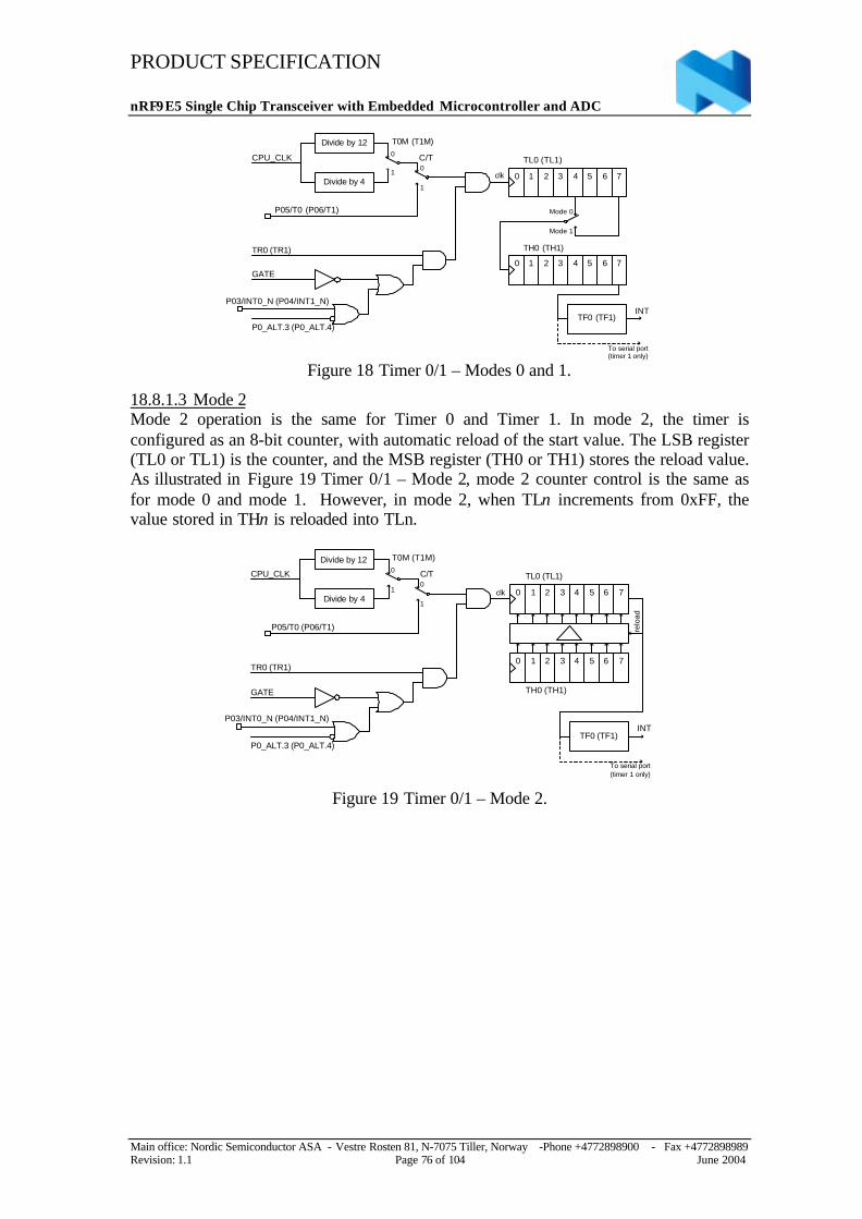
PRODUCT SPECIFICATION
nRF9E5 Single Chip Transceiver with Embedded Microcontroller and ADC
Main office: Nordic Semiconductor ASA - Vestre Rosten 81, N-7075 Tiller, Norway -Phone +4772898900 - Fax +4772898989Revision: 1.1 Page 76 of 104 June 2004
Divide by 12
Divide by 4
CPU_CLK 0
10
1
P05/T0 (P06/T1)
T0M (T1M)
C/T
TR0 (TR1)
GATE
P0_ALT.3 (P0_ALT.4)
P03/INT0_N (P04/INT1_N)
clk
TF0 (TF1)INT
0 1 2 3 4 5 6 7
0 1 2 3 4 5 6 7
Mode 0
Mode 1
TL0 (TL1)
TH0 (TH1)
To serial port(timer 1 only)
Figure 18 Timer 0/1 – Modes 0 and 1.
18.8.1.3 Mode 2Mode 2 operation is the same for Timer 0 and Timer 1. In mode 2, the timer isconfigured as an 8-bit counter, with automatic reload of the start value. The LSB register(TL0 or TL1) is the counter, and the MSB register (TH0 or TH1) stores the reload value.As illustrated in Figure 19 Timer 0/1 – Mode 2, mode 2 counter control is the same asfor mode 0 and mode 1. However, in mode 2, when TLn increments from 0xFF, thevalue stored in THn is reloaded into TLn.
Divide by 12
Divide by 4
CPU_CLK 0
10
1
P05/T0 (P06/T1)
T0M (T1M)
C/T
TR0 (TR1)
GATE
P0_ALT.3 (P0_ALT.4)
P03/INT0_N (P04/INT1_N)
clk
TF0 (TF1)INT
0 1 2 3 4 5 6 7
0 1 2 3 4 5 6 7
TL0 (TL1)
TH0 (TH1)
To serial port(timer 1 only)
relo
ad
Figure 19 Timer 0/1 – Mode 2.
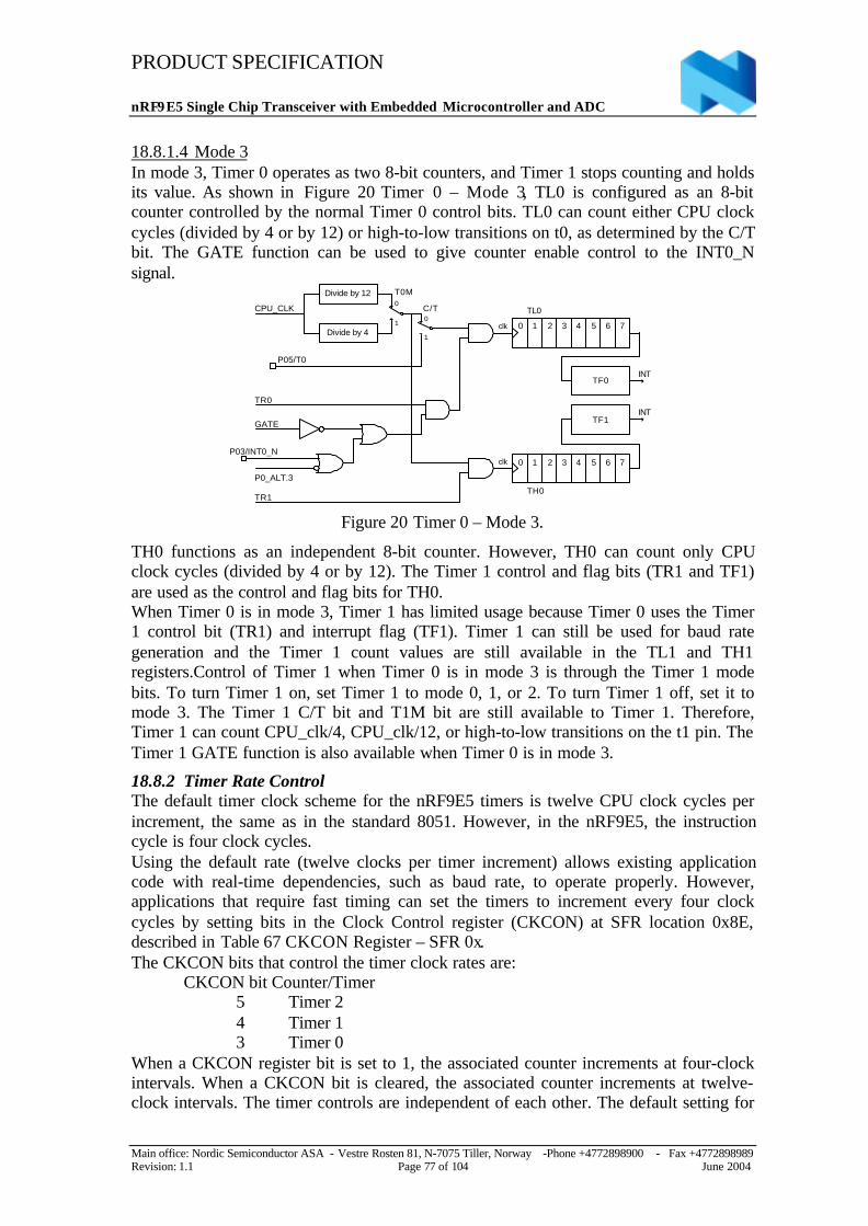
PRODUCT SPECIFICATION
nRF9E5 Single Chip Transceiver with Embedded Microcontroller and ADC
Main office: Nordic Semiconductor ASA - Vestre Rosten 81, N-7075 Tiller, Norway -Phone +4772898900 - Fax +4772898989Revision: 1.1 Page 77 of 104 June 2004
18.8.1.4 Mode 3In mode 3, Timer 0 operates as two 8-bit counters, and Timer 1 stops counting and holdsits value. As shown in Figure 20 Timer 0 – Mode 3, TL0 is configured as an 8-bitcounter controlled by the normal Timer 0 control bits. TL0 can count either CPU clockcycles (divided by 4 or by 12) or high-to-low transitions on t0, as determined by the C/Tbit. The GATE function can be used to give counter enable control to the INT0_Nsignal.
Divide by 12
Divide by 4
CPU_CLK0
10
1
P05/T0
T0M
C/T
TR0
GATE
P0_ALT.3
P03/INT0_N
clk
TF0INT
0 1 2 3 4 5 6 7
0 1 2 3 4 5 6 7
TL0
TH0
TF1INT
clk
TR1
Figure 20 Timer 0 – Mode 3.
TH0 functions as an independent 8-bit counter. However, TH0 can count only CPUclock cycles (divided by 4 or by 12). The Timer 1 control and flag bits (TR1 and TF1)are used as the control and flag bits for TH0.When Timer 0 is in mode 3, Timer 1 has limited usage because Timer 0 uses the Timer1 control bit (TR1) and interrupt flag (TF1). Timer 1 can still be used for baud rategeneration and the Timer 1 count values are still available in the TL1 and TH1registers.Control of Timer 1 when Timer 0 is in mode 3 is through the Timer 1 modebits. To turn Timer 1 on, set Timer 1 to mode 0, 1, or 2. To turn Timer 1 off, set it tomode 3. The Timer 1 C/T bit and T1M bit are still available to Timer 1. Therefore,Timer 1 can count CPU_clk/4, CPU_clk/12, or high-to-low transitions on the t1 pin. TheTimer 1 GATE function is also available when Timer 0 is in mode 3.
18.8.2 Timer Rate ControlThe default timer clock scheme for the nRF9E5 timers is twelve CPU clock cycles perincrement, the same as in the standard 8051. However, in the nRF9E5, the instructioncycle is four clock cycles.Using the default rate (twelve clocks per timer increment) allows existing applicationcode with real-time dependencies, such as baud rate, to operate properly. However,applications that require fast timing can set the timers to increment every four clockcycles by setting bits in the Clock Control register (CKCON) at SFR location 0x8E,described in Table 67 CKCON Register – SFR 0x.The CKCON bits that control the timer clock rates are:
CKCON bit Counter/Timer5 Timer 24 Timer 13 Timer 0
When a CKCON register bit is set to 1, the associated counter increments at four-clockintervals. When a CKCON bit is cleared, the associated counter increments at twelve-clock intervals. The timer controls are independent of each other. The default setting for
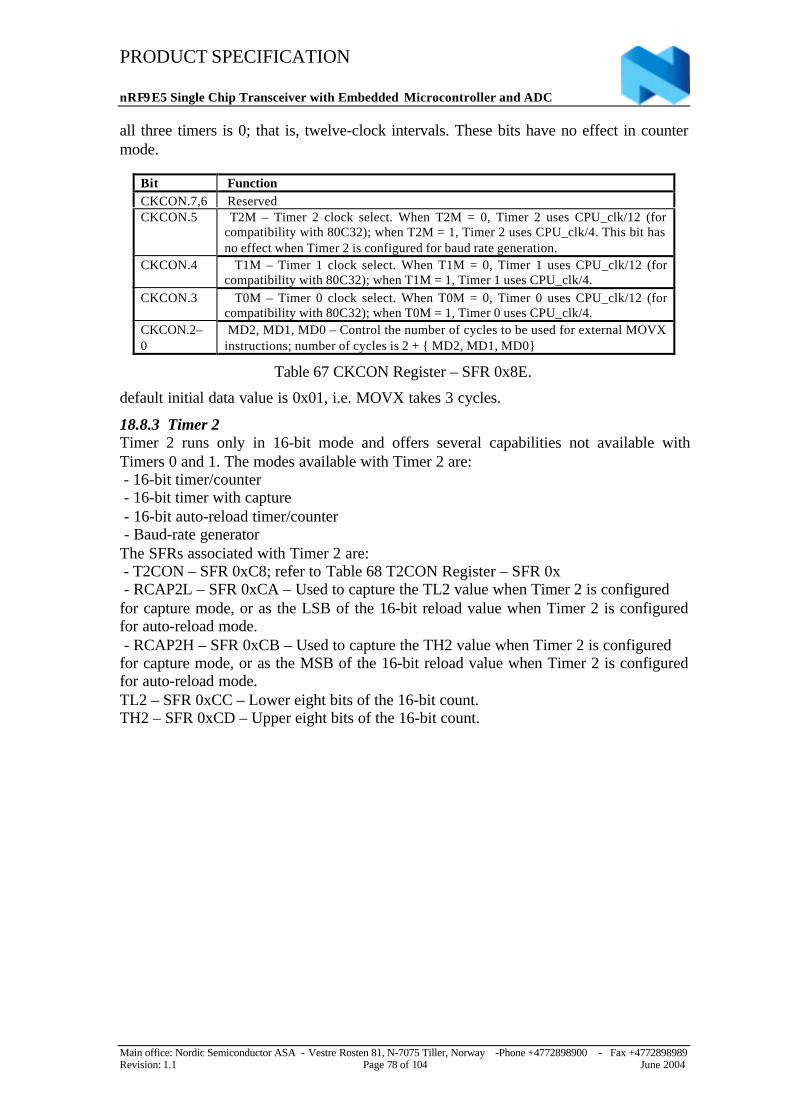
PRODUCT SPECIFICATION
nRF9E5 Single Chip Transceiver with Embedded Microcontroller and ADC
Main office: Nordic Semiconductor ASA - Vestre Rosten 81, N-7075 Tiller, Norway -Phone +4772898900 - Fax +4772898989Revision: 1.1 Page 78 of 104 June 2004
all three timers is 0; that is, twelve-clock intervals. These bits have no effect in countermode.
Bit FunctionCKCON.7,6 ReservedCKCON.5 T2M – Timer 2 clock select. When T2M = 0, Timer 2 uses CPU_clk/12 (for
compatibility with 80C32); when T2M = 1, Timer 2 uses CPU_clk/4. This bit hasno effect when Timer 2 is configured for baud rate generation.
CKCON.4 T1M – Timer 1 clock select. When T1M = 0, Timer 1 uses CPU_clk/12 (forcompatibility with 80C32); when T1M = 1, Timer 1 uses CPU_clk/4.
CKCON.3 T0M – Timer 0 clock select. When T0M = 0, Timer 0 uses CPU_clk/12 (forcompatibility with 80C32); when T0M = 1, Timer 0 uses CPU_clk/4.
CKCON.2–0
MD2, MD1, MD0 – Control the number of cycles to be used for external MOVXinstructions; number of cycles is 2 + MD2, MD1, MD0
Table 67 CKCON Register – SFR 0x8E.
default initial data value is 0x01, i.e. MOVX takes 3 cycles.
18.8.3 Timer 2Timer 2 runs only in 16-bit mode and offers several capabilities not available withTimers 0 and 1. The modes available with Timer 2 are: - 16-bit timer/counter - 16-bit timer with capture - 16-bit auto-reload timer/counter - Baud-rate generatorThe SFRs associated with Timer 2 are: - T2CON – SFR 0xC8; refer to Table 68 T2CON Register – SFR 0x - RCAP2L – SFR 0xCA – Used to capture the TL2 value when Timer 2 is configuredfor capture mode, or as the LSB of the 16-bit reload value when Timer 2 is configuredfor auto-reload mode. - RCAP2H – SFR 0xCB – Used to capture the TH2 value when Timer 2 is configuredfor capture mode, or as the MSB of the 16-bit reload value when Timer 2 is configuredfor auto-reload mode.TL2 – SFR 0xCC – Lower eight bits of the 16-bit count.TH2 – SFR 0xCD – Upper eight bits of the 16-bit count.
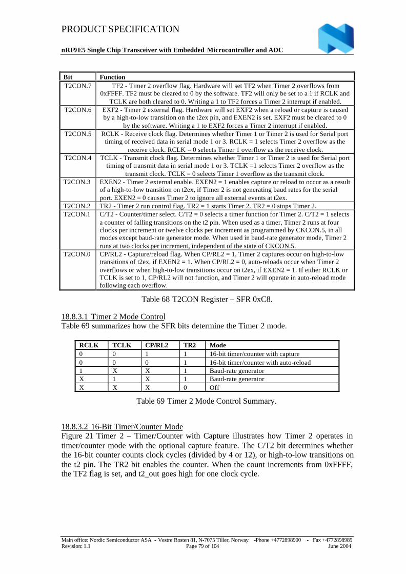
PRODUCT SPECIFICATION
nRF9E5 Single Chip Transceiver with Embedded Microcontroller and ADC
Main office: Nordic Semiconductor ASA - Vestre Rosten 81, N-7075 Tiller, Norway -Phone +4772898900 - Fax +4772898989Revision: 1.1 Page 79 of 104 June 2004
Bit FunctionT2CON.7 TF2 Timer 2 overflow flag. Hardware will set TF2 when Timer 2 overflows from
0xFFFF. TF2 must be cleared to 0 by the software. TF2 will only be set to a 1 if RCLK andTCLK are both cleared to 0. Writing a 1 to TF2 forces a Timer 2 interrupt if enabled.
T2CON.6 EXF2 Timer 2 external flag. Hardware will set EXF2 when a reload or capture is causedby a high-to-low transition on the t2ex pin, and EXEN2 is set. EXF2 must be cleared to 0
by the software. Writing a 1 to EXF2 forces a Timer 2 interrupt if enabled.T2CON.5 RCLK Receive clock flag. Determines whether Timer 1 or Timer 2 is used for Serial port
timing of received data in serial mode 1 or 3. RCLK = 1 selects Timer 2 overflow as thereceive clock. RCLK = 0 selects Timer 1 overflow as the receive clock.
T2CON.4 TCLK Transmit clock flag. Determines whether Timer 1 or Timer 2 is used for Serial porttiming of transmit data in serial mode 1 or 3. TCLK =1 selects Timer 2 overflow as the
transmit clock. TCLK = 0 selects Timer 1 overflow as the transmit clock.T2CON.3 EXEN2 Timer 2 external enable. EXEN2 = 1 enables capture or reload to occur as a result
of a high-to-low transition on t2ex, if Timer 2 is not generating baud rates for the serialport. EXEN2 = 0 causes Timer 2 to ignore all external events at t2ex.
T2CON.2 TR2 Timer 2 run control flag. TR2 = 1 starts Timer 2. TR2 = 0 stops Timer 2.T2CON.1 C/T2 Counter/timer select. C/T2 = 0 selects a timer function for Timer 2. C/T2 = 1 selects
a counter of falling transitions on the t2 pin. When used as a timer, Timer 2 runs at fourclocks per increment or twelve clocks per increment as programmed by CKCON.5, in allmodes except baud-rate generator mode. When used in baud-rate generator mode, Timer 2runs at two clocks per increment, independent of the state of CKCON.5.
T2CON.0 CP/RL2 Capture/reload flag. When CP/RL2 = 1, Timer 2 captures occur on high-to-lowtransitions of t2ex, if EXEN2 = 1. When CP/RL2 = 0, auto-reloads occur when Timer 2overflows or when high-to-low transitions occur on t2ex, if EXEN2 = 1. If either RCLK orTCLK is set to 1, CP/RL2 will not function, and Timer 2 will operate in auto-reload modefollowing each overflow.
Table 68 T2CON Register – SFR 0xC8.
18.8.3.1 Timer 2 Mode ControlTable 69 summarizes how the SFR bits determine the Timer 2 mode.
RCLK TCLK CP/RL2 TR2 Mode0 0 1 1 16-bit timer/counter with capture0 0 0 1 16-bit timer/counter with auto-reload1 X X 1 Baud-rate generatorX 1 X 1 Baud-rate generatorX X X 0 Off
Table 69 Timer 2 Mode Control Summary.
18.8.3.2 16-Bit Timer/Counter ModeFigure 21 Timer 2 – Timer/Counter with Capture illustrates how Timer 2 operates intimer/counter mode with the optional capture feature. The C/T2 bit determines whetherthe 16-bit counter counts clock cycles (divided by 4 or 12), or high-to-low transitions onthe t2 pin. The TR2 bit enables the counter. When the count increments from 0xFFFF,the TF2 flag is set, and t2_out goes high for one clock cycle.
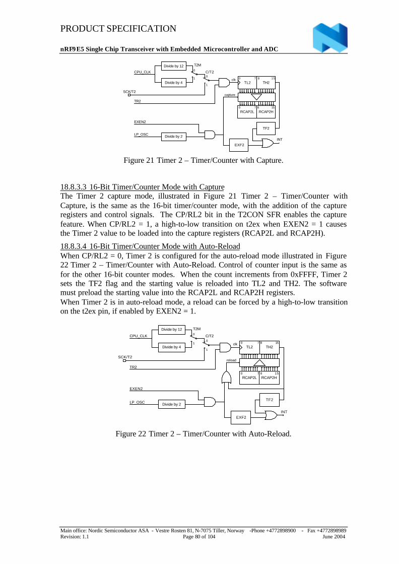
PRODUCT SPECIFICATION
nRF9E5 Single Chip Transceiver with Embedded Microcontroller and ADC
Main office: Nordic Semiconductor ASA - Vestre Rosten 81, N-7075 Tiller, Norway -Phone +4772898900 - Fax +4772898989Revision: 1.1 Page 80 of 104 June 2004
Divide by 12
Divide by 4
CPU_CLK 0
10
1
SCK/T2
T2M
C/T2
TR2
clk
TF2
INT
TL2
capture
0 7
TH28 15
RCAP2L0 7
RCAP2H8 15
EXF2
Divide by 2
EXEN2
LP_OSC
Figure 21 Timer 2 – Timer/Counter with Capture.
18.8.3.3 16-Bit Timer/Counter Mode with CaptureThe Timer 2 capture mode, illustrated in Figure 21 Timer 2 – Timer/Counter withCapture, is the same as the 16-bit timer/counter mode, with the addition of the captureregisters and control signals. The CP/RL2 bit in the T2CON SFR enables the capturefeature. When CP/RL2 = 1, a high-to-low transition on t2ex when EXEN2 = 1 causesthe Timer 2 value to be loaded into the capture registers (RCAP2L and RCAP2H).
18.8.3.4 16-Bit Timer/Counter Mode with Auto-ReloadWhen CP/RL2 = 0, Timer 2 is configured for the auto-reload mode illustrated in Figure22 Timer 2 – Timer/Counter with Auto-Reload. Control of counter input is the same asfor the other 16-bit counter modes. When the count increments from 0xFFFF, Timer 2sets the TF2 flag and the starting value is reloaded into TL2 and TH2. The softwaremust preload the starting value into the RCAP2L and RCAP2H registers.When Timer 2 is in auto-reload mode, a reload can be forced by a high-to-low transitionon the t2ex pin, if enabled by EXEN2 = 1.
Divide by 12
Divide by 4
CPU_CLK 0
10
1
SCK/T2
T2M
C/T2
TR2
clk
TF2
INT
TL2
reload
0 7TH2
8 15
RCAP2L0 7
RCAP2H8 15
EXF2
Divide by 2
EXEN2
LP_OSC
Figure 22 Timer 2 – Timer/Counter with Auto-Reload.
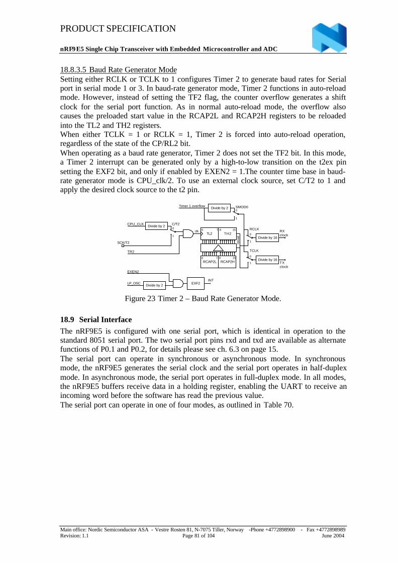
PRODUCT SPECIFICATION
nRF9E5 Single Chip Transceiver with Embedded Microcontroller and ADC
Main office: Nordic Semiconductor ASA - Vestre Rosten 81, N-7075 Tiller, Norway -Phone +4772898900 - Fax +4772898989Revision: 1.1 Page 81 of 104 June 2004
18.8.3.5 Baud Rate Generator ModeSetting either RCLK or TCLK to 1 configures Timer 2 to generate baud rates for Serialport in serial mode 1 or 3. In baud-rate generator mode, Timer 2 functions in auto-reloadmode. However, instead of setting the TF2 flag, the counter overflow generates a shiftclock for the serial port function. As in normal auto-reload mode, the overflow alsocauses the preloaded start value in the RCAP2L and RCAP2H registers to be reloadedinto the TL2 and TH2 registers.When either TCLK = 1 or RCLK = 1, Timer 2 is forced into auto-reload operation,regardless of the state of the CP/RL2 bit.When operating as a baud rate generator, Timer 2 does not set the TF2 bit. In this mode,a Timer 2 interrupt can be generated only by a high-to-low transition on the t2ex pinsetting the EXF2 bit, and only if enabled by EXEN2 = 1.The counter time base in baud-rate generator mode is CPU_clk/2. To use an external clock source, set C/T2 to 1 andapply the desired clock source to the t2 pin.
Divide by 2CPU_CLK0
1
SCK/T2
C/T2
TR2
clk
INT
TL20 7
TH28 15
RCAP2L0 7
RCAP2H8 15
EXF2Divide by 2
EXEN2
LP_OSC
RCLK0
1
TCLK
0
1Divide by 16
Divide by 16
TXclock
RXclock
Divide by 20
1
Timer 1 overflow SMOD0
relo
ad
Figure 23 Timer 2 – Baud Rate Generator Mode.
18.9 Serial InterfaceThe nRF9E5 is configured with one serial port, which is identical in operation to thestandard 8051 serial port. The two serial port pins rxd and txd are available as alternatefunctions of P0.1 and P0.2, for details please see ch. 6.3 on page 15.The serial port can operate in synchronous or asynchronous mode. In synchronousmode, the nRF9E5 generates the serial clock and the serial port operates in half-duplexmode. In asynchronous mode, the serial port operates in full-duplex mode. In all modes,the nRF9E5 buffers receive data in a holding register, enabling the UART to receive anincoming word before the software has read the previous value.The serial port can operate in one of four modes, as outlined in Table 70.
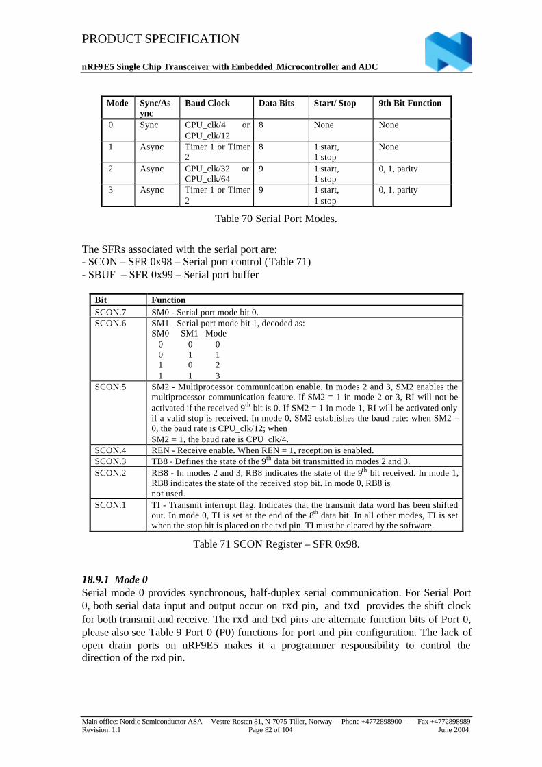
PRODUCT SPECIFICATION
nRF9E5 Single Chip Transceiver with Embedded Microcontroller and ADC
Main office: Nordic Semiconductor ASA - Vestre Rosten 81, N-7075 Tiller, Norway -Phone +4772898900 - Fax +4772898989Revision: 1.1 Page 82 of 104 June 2004
Mode Sync/Async
Baud Clock Data Bits Start/ Stop 9th Bit Function
0 Sync CPU_clk/4 orCPU_clk/12
8 None None
1 Async Timer 1 or Timer2
8 1 start,1 stop
None
2 Async CPU_clk/32 orCPU_clk/64
9 1 start,1 stop
0, 1, parity
3 Async Timer 1 or Timer2
9 1 start,1 stop
0, 1, parity
Table 70 Serial Port Modes.
The SFRs associated with the serial port are:- SCON – SFR 0x98 – Serial port control (Table 71)- SBUF – SFR 0x99 – Serial port buffer
Bit FunctionSCON.7 SM0 Serial port mode bit 0.SCON.6 SM1 Serial port mode bit 1, decoded as:
SM0 SM1 Mode 0 0 0 0 1 1 1 0 2 1 1 3
SCON.5 SM2 Multiprocessor communication enable. In modes 2 and 3, SM2 enables themultiprocessor communication feature. If SM2 = 1 in mode 2 or 3, RI will not beactivated if the received 9th bit is 0. If SM2 = 1 in mode 1, RI will be activated onlyif a valid stop is received. In mode 0, SM2 establishes the baud rate: when SM2 =0, the baud rate is CPU_clk/12; whenSM2 = 1, the baud rate is CPU_clk/4.
SCON.4 REN Receive enable. When REN = 1, reception is enabled.SCON.3 TB8 Defines the state of the 9th data bit transmitted in modes 2 and 3.SCON.2 RB8 In modes 2 and 3, RB8 indicates the state of the 9th bit received. In mode 1,
RB8 indicates the state of the received stop bit. In mode 0, RB8 isnot used.
SCON.1 TI Transmit interrupt flag. Indicates that the transmit data word has been shiftedout. In mode 0, TI is set at the end of the 8th data bit. In all other modes, TI is setwhen the stop bit is placed on the txd pin. TI must be cleared by the software.
Table 71 SCON Register – SFR 0x98.
18.9.1 Mode 0Serial mode 0 provides synchronous, half-duplex serial communication. For Serial Port0, both serial data input and output occur on rxd pin, and txd provides the shift clockfor both transmit and receive. The rxd and txd pins are alternate function bits of Port 0,please also see Table 9 Port 0 (P0) functions for port and pin configuration. The lack ofopen drain ports on nRF9E5 makes it a programmer responsibility to control thedirection of the rxd pin.
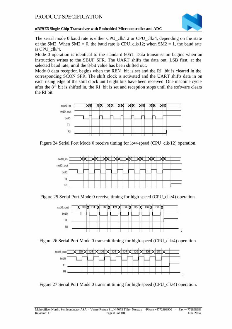
PRODUCT SPECIFICATION
nRF9E5 Single Chip Transceiver with Embedded Microcontroller and ADC
Main office: Nordic Semiconductor ASA - Vestre Rosten 81, N-7075 Tiller, Norway -Phone +4772898900 - Fax +4772898989Revision: 1.1 Page 83 of 104 June 2004
The serial mode 0 baud rate is either CPU_clk/12 or CPU_clk/4, depending on the stateof the SM2. When SM2 = 0, the baud rate is CPU_clk/12; when SM2 = 1, the baud rateis CPU_clk/4.Mode 0 operation is identical to the standard 8051. Data transmission begins when aninstruction writes to the SBUF SFR. The UART shifts the data out, LSB first, at theselected baud rate, until the 8-bit value has been shifted out.Mode 0 data reception begins when the REN bit is set and the RI bit is cleared in thecorresponding SCON SFR. The shift clock is activated and the UART shifts data in oneach rising edge of the shift clock until eight bits have been received. One machine cycleafter the 8th bit is shifted in, the RI bit is set and reception stops until the software clearsthe RI bit.
Figure 24 Serial Port Mode 0 receive timing for low-speed (CPU_clk/12) operation.
Figure 25 Serial Port Mode 0 receive timing for high-speed (CPU_clk/4) operation.
:
Figure 26 Serial Port Mode 0 transmit timing for high-speed (CPU_clk/4) operation.
:
Figure 27 Serial Port Mode 0 transmit timing for high-speed (CPU_clk/4) operation.
PRODUCT SPECIFICATION
nRF9E5 Single Chip Transceiver with Embedded Microcontroller and ADC
Main office: Nordic Semiconductor ASA - Vestre Rosten 81, N-7075 Tiller, Norway -Phone +4772898900 - Fax +4772898989Revision: 1.1 Page 84 of 104 June 2004
18.9.2 Mode 1Mode 1 provides standard asynchronous, full-duplex communication, using a total of tenbits: one start bit, eight data bits, and one stop bit. For receive operations, the stop bit isstored in RB8. Data bits are received and transmitted LSB first.
18.9.2.1 Mode 1 Baud RateThe mode 1 baud rate is a function of timer overflow. Serial port can use either Timer 1or Timer 2 to generate baud rates. Each time the timer increments from its maximumcount (0xFF for Timer 1 or 0xFFFF for Timer 2), a clock is sent to the baud-rate circuit.The clock is then divided by 16 to generate the baud rate. When using Timer 1, theSMOD bit selects whether or not to divide the Timer 1 rollover rate by 2. Therefore,when using Timer 1, the baud rate is determinedby the equation:
Baud Rate = 32
2SMOD
x Timer 1 Overflow
SMOD is SFR bit PCON.7
When using Timer 2, the baud rate is determined by the equation:
Baud Rate = 16
Overflow 2Timer
To use Timer 1 as the baud-rate generator, it is best to use Timer 1 mode 2 (8-bit counterwith auto-reload), although any counter mode can be used. The Timer 1 reload value isstored in the TH1 register, which makes the complete formula for Timer 1:
Baud Rate = 32
2SMOD
x TH1)- (256 x 4
clk
The 4 in the denominator in the above equation can be obtained by setting the T1M bitin the CKCON SFR. To derive the required TH1 value from a known baud rate (whenTM1 = 0), use the equation:
TH1 = 256 - Rate Baud128
2∗
∗clkSMOD
You can also achieve very low serial port baud rates from Timer 1 by enabling theTimer 1 interrupt, configuring Timer 1 to mode 1, and using the Timer 1 interrupt toinitiate a 16-bit software reload. Table Table 72 lists sample reload values for a varietyof common serial port baud rates.
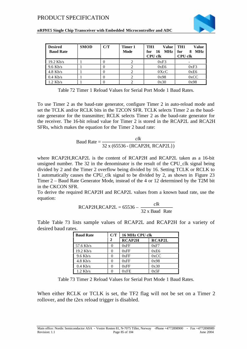
PRODUCT SPECIFICATION
nRF9E5 Single Chip Transceiver with Embedded Microcontroller and ADC
Main office: Nordic Semiconductor ASA - Vestre Rosten 81, N-7075 Tiller, Norway -Phone +4772898900 - Fax +4772898989Revision: 1.1 Page 85 of 104 June 2004
Desired Baud Rate
SMOD C/T Timer 1 Mode
TH1 Valuefor 16 MHzCPU clk
TH1 Valuefor 8 MHzCPU clk
19.2 Kb/s 1 0 2 0xF3 -9.6 Kb/s 1 0 2 0xE6 0xF34.8 Kb/s 1 0 2 0XcC 0xE60.4 Kb/s 1 0 2 0x98 0xCC1.2 Kb/s 1 0 2 0x30 0x98
Table 72 Timer 1 Reload Values for Serial Port Mode 1 Baud Rates.
To use Timer 2 as the baud-rate generator, configure Timer 2 in auto-reload mode andset the TCLK and/or RCLK bits in the T2CON SFR. TCLK selects Timer 2 as the baud-rate generator for the transmitter; RCLK selects Timer 2 as the baud-rate generator forthe receiver. The 16-bit reload value for Timer 2 is stored in the RCAP2L and RCA2HSFRs, which makes the equation for the Timer 2 baud rate:
Baud Rate =RCAP2L)RCAP2H, - (65536 x 32
clk
where RCAP2H,RCAP2L is the content of RCAP2H and RCAP2L taken as a 16-bitunsigned number. The 32 in the denominator is the result of the CPU_clk signal beingdivided by 2 and the Timer 2 overflow being divided by 16. Setting TCLK or RCLK to1 automatically causes the CPU_clk signal to be divided by 2, as shown in Figure 23Timer 2 – Baud Rate Generator Mode, instead of the 4 or 12 determined by the T2M bitin the CKCON SFR.To derive the required RCAP2H and RCAP2L values from a known baud rate, use theequation:
RCAP2H,RCAP2L = 65536 – Rate Baud x 32
clk
Table Table 73 lists sample values of RCAP2L and RCAP2H for a variety ofdesired baud rates.
16 MHz CPU clkBaud Rate C/T2 RCAP2H RCAP2L
57.6 Kb/s 0 0xFF 0xF719.2 Kb/s 0 0xFF 0xE6 9.6 Kb/s 0 0xFF 0xCC 4.8 Kb/s 0 0xFF 0x98 0.4 Kb/s 0 0xFF 0x30 1.2 Kb/s 0 0xFE 0x5F
Table 73 Timer 2 Reload Values for Serial Port Mode 1 Baud Rates.
When either RCLK or TCLK is set, the TF2 flag will not be set on a Timer 2rollover, and the t2ex reload trigger is disabled.
PRODUCT SPECIFICATION
nRF9E5 Single Chip Transceiver with Embedded Microcontroller and ADC
Main office: Nordic Semiconductor ASA - Vestre Rosten 81, N-7075 Tiller, Norway -Phone +4772898900 - Fax +4772898989Revision: 1.1 Page 86 of 104 June 2004
18.9.2.2 Mode 1 Transmit
Figure 28 illustrates the mode 1 transmit timing. In mode 1, the UART beginstransmitting after the first rollover of the divide-by-16 counter after the software writesto the SBUF register. The UART transmits data on the txd pin in the following order:start bit, eight data bits (LSB first), stop bit. The TI bit is set two clock cycles after thestop bit is transmitted.
Figure 28 Serial port Mode 1 Transmit Timing.
18.9.2.3 Mode 1 Receive
Figure 29 illustrates the mode 1 receive timing. Reception begins at the falling edge of astart bit received on rxd_in, when enabled by the REN bit. For this purpose, rxd_in issampled sixteen times per bit for any baud rate. When a falling edge of a start bit isdetected, the divide-by-16 counter used to generate the receive clock is reset to align thecounter rollover to the bit boundaries.
Figure 29 Serial port Mode 1 Receive Timing.
PRODUCT SPECIFICATION
nRF9E5 Single Chip Transceiver with Embedded Microcontroller and ADC
Main office: Nordic Semiconductor ASA - Vestre Rosten 81, N-7075 Tiller, Norway -Phone +4772898900 - Fax +4772898989Revision: 1.1 Page 87 of 104 June 2004
For noise rejection, the serial port establishes the content of each received bit by amajority decision of three consecutive samples in the middle of each bit time. This isespecially true for the start bit. If the falling edge on rxd_in is not verified by a majoritydecision of three consecutive samples (low), then the serial port stops reception andwaits for another falling edge on rxd_in.At the middle of the stop bit time, the serial port checks for the following conditions: -?RI = 0 - If SM2 = 1, the state of the stop bit is 1 (if SM2 = 0, the state of the stop bit does not matter)
If the above conditions are met, the serial port then writes the received byte to the SBUFregister, loads the stop bit into RB8, and sets the RI bit. If the above conditions are notmet, the received data is lost, the SBUF register and RB8 bit are not loaded, and the RIbit is not set. After the middle of the stop bit time, the serial port waits for another high-to-low transition on the rxd_in pin.Mode 1 operation is identical to that of the standard 8051 when Timers 1 and 2 useCPU_clk/12 (the default).
18.9.3 Mode 2Mode 2 provides asynchronous, full-duplex communication, using a total of eleven bits: - One start bit - Eight data bits - One programmable 9th bit - One stop bitThe data bits are transmitted and received LSB first. For transmission, the 9th bit isdetermined by the value in TB8. To use the 9th bit as a parity bit, move the value of theP bit (SFR PSW.0) to TB8.The mode 2 baud rate is either CPU_clk/32 or CPU_clk/64, as determined by the SMODbit. The formula for the mode 2 baud rate is:
Baud Rate = 64
2 clkSMOD ∗
Mode 2 operation is identical to the standard 8051.
18.9.3.1 Mode 2 Transmit
Figure 30 illustrates the mode 2 transmit timing. Transmission begins after the firstrollover of the divide-by-16 counter following a software write to SBUF . The UARTshifts data out on the txd pin in the following order: start bit, data bits (LSB first), 9thbit, stop bit. The TI bit is set when the stop bit is placed on the txd pin.
PRODUCT SPECIFICATION
nRF9E5 Single Chip Transceiver with Embedded Microcontroller and ADC
Main office: Nordic Semiconductor ASA - Vestre Rosten 81, N-7075 Tiller, Norway -Phone +4772898900 - Fax +4772898989Revision: 1.1 Page 88 of 104 June 2004
Figure 30 Serial port Mode 2 Transmit Timing.
PRODUCT SPECIFICATION
nRF9E5 Single Chip Transceiver with Embedded Microcontroller and ADC
Main office: Nordic Semiconductor ASA - Vestre Rosten 81, N-7075 Tiller, Norway -Phone +4772898900 - Fax +4772898989Revision: 1.1 Page 89 of 104 June 2004
18.9.3.2 Mode 2 Receive
Figure 31 illustrates the mode 2 receive timing. Reception begins at the falling edge of astart bit received on rxd_in, when enabled by the REN bit. For this purpose, rxd_in issampled sixteen times per bit for any baud rate. When a falling edge of a start bit isdetected, the divide-by-16 counter used to generate the receive clock is reset to align thecounter rollover to the bit boundaries.
Figure 31 Serial port Mode 2 Receive Timing.
For noise rejection, the serial port establishes the content of each received bit by amajority decision of three consecutive samples in the middle of each bit time. This isespecially true for the start bit. If the falling edge on rxd_in is not verified by a majoritydecision of three consecutive samples (low), then the serial port stops reception andwaits for another falling edge on rxd_in.At the middle of the stop bit time, the serial port checks for the following conditions: - RI = 0 - If SM2 = 1, the state of the stop bit is 1 (if SM2 = 0, the state of the stop bit does not matter)If the above conditions are met, the serial port then writes the received byte to the SBUFregister, loads the 9th received bit into RB8, and sets the RI bit. If the above conditionsare not met, the received data is lost, the SBUF register and RB8 bit are not loaded, andthe RI bit is not set. After the middle of the stop bit time, the serial port waits for anotherhigh-to-low transition on the rxd_in.
18.9.4 Mode 3Mode 3 provides asynchronous, full-duplex communication, using a total of eleven bits: - One start bit - Eight data bits - One programmable 9th bit - One stop bit; the data bits are transmitted and received LSB firstThe mode 3 transmit and receive operations are identical to mode 2. The mode 3 baudrate generation is identical to mode 1. That is, mode 3 is a combination of mode 2protocol and mode 1 baud rate. Figure 32 illustrates the mode 3 transmit timing. Mode 3operation is identical to that of the standard 8051 when Timers 1 and 2 use CPU_clk/12(the default).
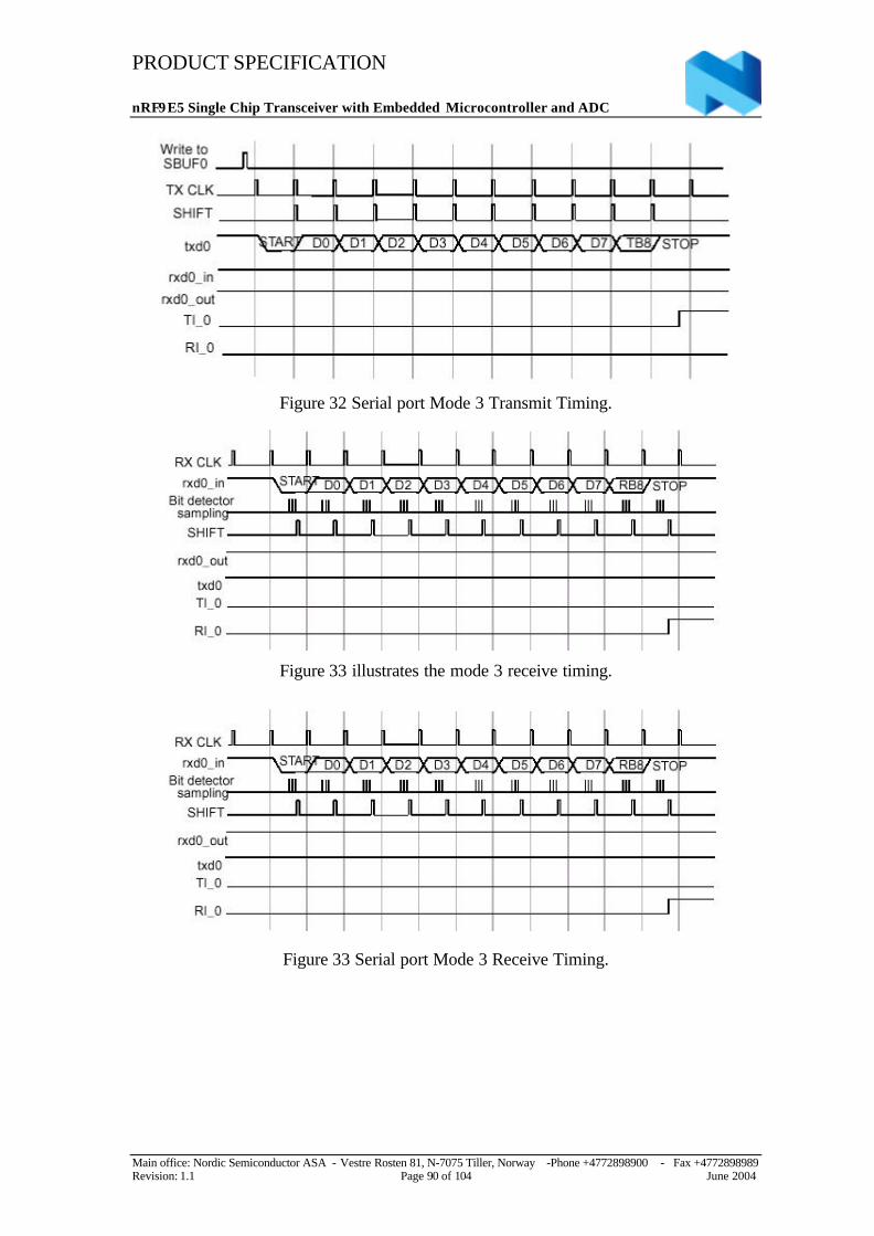
PRODUCT SPECIFICATION
nRF9E5 Single Chip Transceiver with Embedded Microcontroller and ADC
Main office: Nordic Semiconductor ASA - Vestre Rosten 81, N-7075 Tiller, Norway -Phone +4772898900 - Fax +4772898989Revision: 1.1 Page 90 of 104 June 2004
Figure 32 Serial port Mode 3 Transmit Timing.
Figure 33 illustrates the mode 3 receive timing.
Figure 33 Serial port Mode 3 Receive Timing.
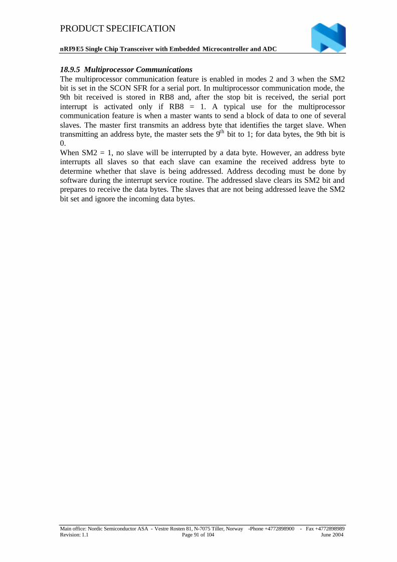
PRODUCT SPECIFICATION
nRF9E5 Single Chip Transceiver with Embedded Microcontroller and ADC
Main office: Nordic Semiconductor ASA - Vestre Rosten 81, N-7075 Tiller, Norway -Phone +4772898900 - Fax +4772898989Revision: 1.1 Page 91 of 104 June 2004
18.9.5 Multiprocessor CommunicationsThe multiprocessor communication feature is enabled in modes 2 and 3 when the SM2bit is set in the SCON SFR for a serial port. In multiprocessor communication mode, the9th bit received is stored in RB8 and, after the stop bit is received, the serial portinterrupt is activated only if RB8 = 1. A typical use for the multiprocessorcommunication feature is when a master wants to send a block of data to one of severalslaves. The master first transmits an address byte that identifies the target slave. Whentransmitting an address byte, the master sets the 9th bit to 1; for data bytes, the 9th bit is0.When SM2 = 1, no slave will be interrupted by a data byte. However, an address byteinterrupts all slaves so that each slave can examine the received address byte todetermine whether that slave is being addressed. Address decoding must be done bysoftware during the interrupt service routine. The addressed slave clears its SM2 bit andprepares to receive the data bytes. The slaves that are not being addressed leave the SM2bit set and ignore the incoming data bytes.
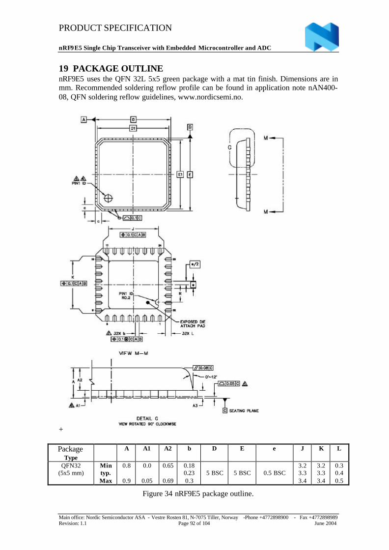
PRODUCT SPECIFICATION
nRF9E5 Single Chip Transceiver with Embedded Microcontroller and ADC
Main office: Nordic Semiconductor ASA - Vestre Rosten 81, N-7075 Tiller, Norway -Phone +4772898900 - Fax +4772898989Revision: 1.1 Page 92 of 104 June 2004
19 PACKAGE OUTLINEnRF9E5 uses the QFN 32L 5x5 green package with a mat tin finish. Dimensions are inmm. Recommended soldering reflow profile can be found in application note nAN400-08, QFN soldering reflow guidelines, www.nordicsemi.no.
+
PackageType
A A1 A2 b D E e J K L
QFN32(5x5 mm)
Mintyp.Max
0.8
0.9
0.0
0.05
0.65
0.69
0.180.230.3
5 BSC 5 BSC 0.5 BSC3.23.33.4
3.23.33.4
0.30.40.5
Figure 34 nRF9E5 package outline.

PRODUCT SPECIFICATION
nRF9E5 Single Chip Transceiver with Embedded Microcontroller and ADC
Main office: Nordic Semiconductor ASA - Vestre Rosten 81, N-7075 Tiller, Norway -Phone +4772898900 - Fax +4772898989Revision: 1.1 Page 93 of 104 June 2004
20 PCB LAYOUT AND DECOUPLING GUIDELINESnRF9E5 is an extremely robust RF device due to internal voltage regulators and requiresthe minimum of RF layout protocols. However the following design rules should still beincorporated into the layout design.
A PCB with a minimum of two layers including a ground plane is recommended foroptimum performance. The nRF9E5 DC supply voltage should be decoupled as close aspossible to the VDD pins with high performance RF capacitors. It is preferable to mounta large surface mount capacitor (e.g. 4.7µF tantalum) in parallel with the smaller valuecapacitors. The nRF9E5 supply voltage should be filtered and routed separately from thesupply voltages of any digital circuitry.
Long power supply lines on the PCB should be avoided. All device grounds, VDDconnections and VDD bypass capacitors must be connected as close as possible to thenRF9E5 IC. For a PCB with a topside RF ground plane, the VSS pins should beconnected directly to the ground plane. For a PCB with a bottom ground plane, the besttechnique is to place via holes as close as possible to the VSS pins. A minimum of onevia hole should be used for each VSS pin.
Full swing digital data or control signals should not be routed close to the crystal or thepower supply lines.
A fully qualified RF-layout for the nRF9E5 and its surrounding components, includingantennas and matching networks, can be downloaded from www.nordicsemi.no.
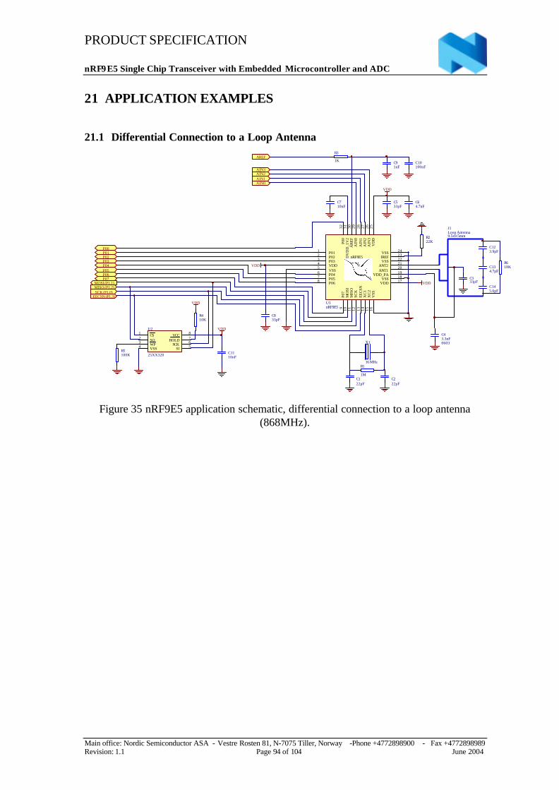
PRODUCT SPECIFICATION
nRF9E5 Single Chip Transceiver with Embedded Microcontroller and ADC
Main office: Nordic Semiconductor ASA - Vestre Rosten 81, N-7075 Tiller, Norway -Phone +4772898900 - Fax +4772898989Revision: 1.1 Page 94 of 104 June 2004
21 APPLICATION EXAMPLES
21.1 Differential Connection to a Loop Antenna
P011 VSS 24
VSS 18
VDD 17
VSS
16
P022
P033
VDD4
VSS5
P046
P057
P068
P07
9
MO
SI10
MIS
O11
SCK
12
XC
215
XC
114
EEC
SN13
VDD_PA 19ANT120ANT2 21VSS 22IREF 23nRF9E5
VD
D25
AIN
326
AIN
227
AIN
128
AIN
029
AR
EF30
DV
DD
_1V
231
P00
32
U1nRF9E5
C91nF
R3
1K C10100nF
CS1
SO2
WP3
VSS4 SI 5SCK 6HOLD 7VCC 8
U2
25XX320 C1110nF
R410K
R5100K
VDD
VDD
C222pF
C64.7nF
C533pF
R222K
C710nF
VDD
C122pF
R1
1M
X1
16 MHz
C833pF
VDD
MOSI (P1.1)MISO (P1.2)SCK (P1.0)
EECSN (P1.3)
P00P01P02P03P04P05P06P07
AIN0AIN1AIN2AIN3
AREF
VDD
C43.3nF0603
C333pF
R618KC13
4.7pF
C145.6pF
aaaaaaaa
J1Loop Antenna9.5x9.5mm
C123.9pF
aaaaaaaa
aaaaaaaa
aaaa
aaaa
Figure 35 nRF9E5 application schematic, differential connection to a loop antenna(868MHz).
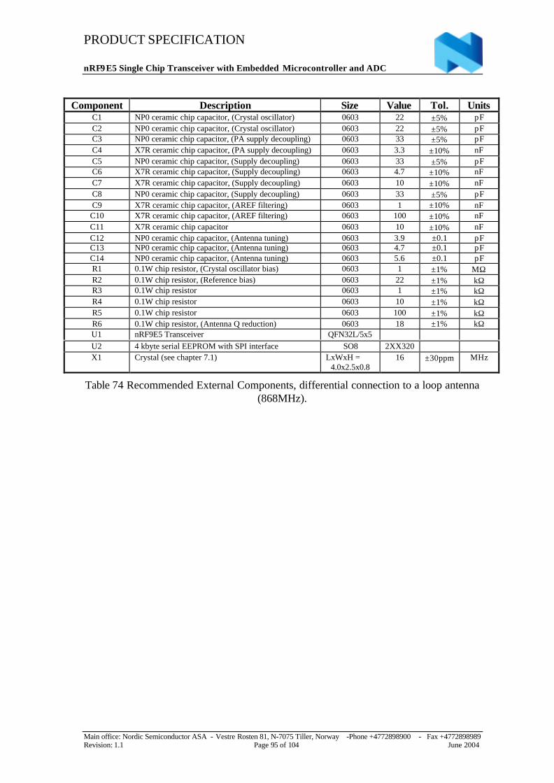
PRODUCT SPECIFICATION
nRF9E5 Single Chip Transceiver with Embedded Microcontroller and ADC
Main office: Nordic Semiconductor ASA - Vestre Rosten 81, N-7075 Tiller, Norway -Phone +4772898900 - Fax +4772898989Revision: 1.1 Page 95 of 104 June 2004
Component Description Size Value Tol. UnitsC1 NP0 ceramic chip capacitor, (Crystal oscillator) 0603 22 ±5% pFC2 NP0 ceramic chip capacitor, (Crystal oscillator) 0603 22 ±5% pFC3 NP0 ceramic chip capacitor, (PA supply decoupling) 0603 33 ±5% pFC4 X7R ceramic chip capacitor, (PA supply decoupling) 0603 3.3 ±10% nFC5 NP0 ceramic chip capacitor, (Supply decoupling) 0603 33 ±5% pFC6 X7R ceramic chip capacitor, (Supply decoupling) 0603 4.7 ±10% nFC7 X7R ceramic chip capacitor, (Supply decoupling) 0603 10 ±10% nFC8 NP0 ceramic chip capacitor, (Supply decoupling) 0603 33 ±5% pFC9 X7R ceramic chip capacitor, (AREF filtering) 0603 1 ±10% nFC10 X7R ceramic chip capacitor, (AREF filtering) 0603 100 ±10% nFC11 X7R ceramic chip capacitor 0603 10 ±10% nFC12 NP0 ceramic chip capacitor, (Antenna tuning) 0603 3.9 ±0.1 pFC13 NP0 ceramic chip capacitor, (Antenna tuning) 0603 4.7 ±0.1 pFC14 NP0 ceramic chip capacitor, (Antenna tuning) 0603 5.6 ±0.1 pFR1 0.1W chip resistor, (Crystal oscillator bias) 0603 1 ±1% MΩR2 0.1W chip resistor, (Reference bias) 0603 22 ±1% kΩR3 0.1W chip resistor 0603 1 ±1% kΩR4 0.1W chip resistor 0603 10 ±1% kΩR5 0.1W chip resistor 0603 100 ±1% kΩR6 0.1W chip resistor, (Antenna Q reduction) 0603 18 ±1% kΩU1 nRF9E5 Transceiver QFN32L/5x5U2 4 kbyte serial EEPROM with SPI interface SO8 2XX320X1 Crystal (see chapter 7.1) LxWxH =
4.0x2.5x0.816 ±30ppm MHz
Table 74 Recommended External Components, differential connection to a loop antenna(868MHz).
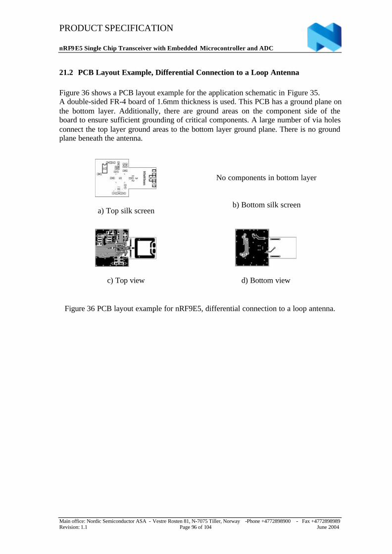
PRODUCT SPECIFICATION
nRF9E5 Single Chip Transceiver with Embedded Microcontroller and ADC
Main office: Nordic Semiconductor ASA - Vestre Rosten 81, N-7075 Tiller, Norway -Phone +4772898900 - Fax +4772898989Revision: 1.1 Page 96 of 104 June 2004
21.2 PCB Layout Example, Differential Connection to a Loop Antenna
Figure 36 shows a PCB layout example for the application schematic in Figure 35.A double-sided FR-4 board of 1.6mm thickness is used. This PCB has a ground plane onthe bottom layer. Additionally, there are ground areas on the component side of theboard to ensure sufficient grounding of critical components. A large number of via holesconnect the top layer ground areas to the bottom layer ground plane. There is no groundplane beneath the antenna.
a) Top silk screen
No components in bottom layer
b) Bottom silk screen
c) Top view d) Bottom view
Figure 36 PCB layout example for nRF9E5, differential connection to a loop antenna.
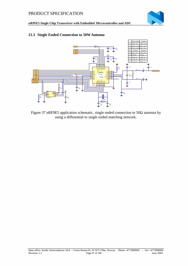
PRODUCT SPECIFICATION
nRF9E5 Single Chip Transceiver with Embedded Microcontroller and ADC
Main office: Nordic Semiconductor ASA - Vestre Rosten 81, N-7075 Tiller, Norway -Phone +4772898900 - Fax +4772898989Revision: 1.1 Page 97 of 104 June 2004
21.3 Single Ended Connection to 50Ω Antenna
P011 VSS 24
VSS18
VDD 17
VSS
16
P022
P033
VDD4
VSS5
P046
P057
P068
P07
9
MO
SI10
MIS
O11
SCK
12
XC
215
XC
114
EE
CSN
13
VDD_PA19ANT1 20
ANT2 21VSS22IREF 23nRF9E5
VD
D25
AIN
326
AIN
227
AIN
128
AIN
029
AR
EF
30D
VD
D_1
V2
31P0
032
U1nRF9E5
C91nF
R3
1KC10100nF
CS1
SO2
WP3
VSS4 SI 5SCK6HOLD7VCC 8
U2
25XX320 C1110nF
R410K
R5100K
VDD
VDD
C222pF
C64.7nF
C533pF
R222K
C710nF
VDD
C122pF
R1
1M
X1
16 MHz
VDD
L1
C3
C14Not fitted
C15
L3
L2
C12
C13
C43.3nF
C833pF
VDD
C16
C3
C12
C13
C14
C15
C16
L1
L2
L3
868/915MHz 433MHz
33pF, ±5%
3.9pF, ±0.25pF
3.9pF, ±0.25pF
Not fitted Not fitted
33pF, ±5%
Not fitted
12nH, 5%
12nH, 5%
12nH, 5%
180pF, ±5%
18pF, ±5%
18pF, ±5%
6.8pF, ±5%
Not fitted
12nH, 5%
39nH, 5%
39nH, 5%
MOSI (P1.1)MISO (P1.2)SCK (P1.0)
EECSN (P1.3)
P00P01P02P03P04P05P06P07
AIN0AIN1AIN2AIN3
AREF
50 ohm RF I/O
aaaaaaaa
aaaaaaaa
aaaa
aaaa
aaaaaaaa
Figure 37 nRF9E5 application schematic, single ended connection to 50Ω antenna byusing a differential to single ended matching network.
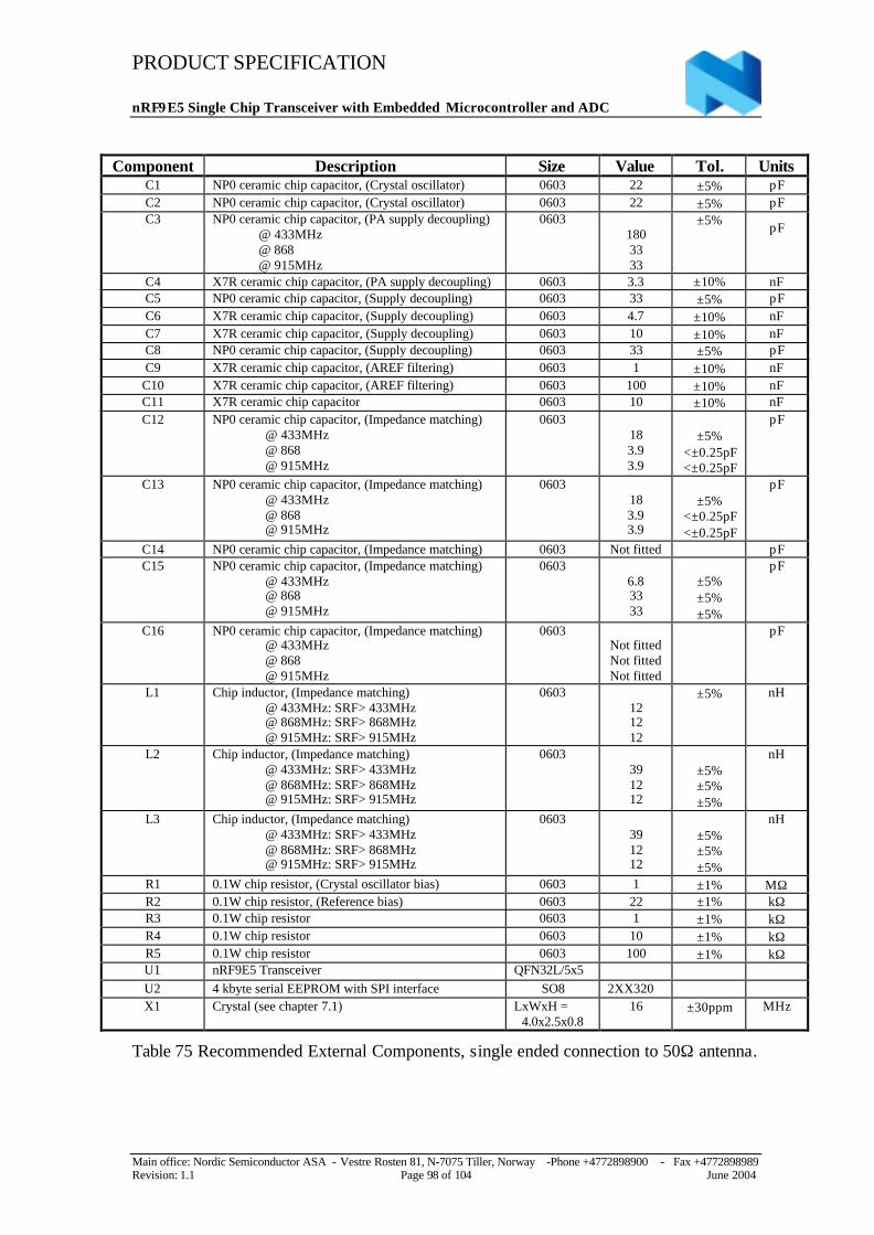
PRODUCT SPECIFICATION
nRF9E5 Single Chip Transceiver with Embedded Microcontroller and ADC
Main office: Nordic Semiconductor ASA - Vestre Rosten 81, N-7075 Tiller, Norway -Phone +4772898900 - Fax +4772898989Revision: 1.1 Page 98 of 104 June 2004
Component Description Size Value Tol. UnitsC1 NP0 ceramic chip capacitor, (Crystal oscillator) 0603 22 ±5% pFC2 NP0 ceramic chip capacitor, (Crystal oscillator) 0603 22 ±5% pFC3 NP0 ceramic chip capacitor, (PA supply decoupling)
@ 433MHz@ 868@ 915MHz
06031803333
±5% pF
C4 X7R ceramic chip capacitor, (PA supply decoupling) 0603 3.3 ±10% nFC5 NP0 ceramic chip capacitor, (Supply decoupling) 0603 33 ±5% pFC6 X7R ceramic chip capacitor, (Supply decoupling) 0603 4.7 ±10% nFC7 X7R ceramic chip capacitor, (Supply decoupling) 0603 10 ±10% nFC8 NP0 ceramic chip capacitor, (Supply decoupling) 0603 33 ±5% pFC9 X7R ceramic chip capacitor, (AREF filtering) 0603 1 ±10% nFC10 X7R ceramic chip capacitor, (AREF filtering) 0603 100 ±10% nFC11 X7R ceramic chip capacitor 0603 10 ±10% nFC12 NP0 ceramic chip capacitor, (Impedance matching)
@ 433MHz@ 868@ 915MHz
0603183.93.9
±5%<±0.25pF<±0.25pF
pF
C13 NP0 ceramic chip capacitor, (Impedance matching)@ 433MHz@ 868@ 915MHz
0603183.93.9
±5%<±0.25pF<±0.25pF
pF
C14 NP0 ceramic chip capacitor, (Impedance matching) 0603 Not fitted pFC15 NP0 ceramic chip capacitor, (Impedance matching)
@ 433MHz@ 868@ 915MHz
06036.83333
±5%±5%±5%
pF
C16 NP0 ceramic chip capacitor, (Impedance matching)@ 433MHz@ 868@ 915MHz
0603Not fittedNot fittedNot fitted
pF
L1 Chip inductor, (Impedance matching)@ 433MHz: SRF> 433MHz@ 868MHz: SRF> 868MHz@ 915MHz: SRF> 915MHz
0603121212
±5% nH
L2 Chip inductor, (Impedance matching)@ 433MHz: SRF> 433MHz@ 868MHz: SRF> 868MHz@ 915MHz: SRF> 915MHz
0603391212
±5%±5%±5%
nH
L3 Chip inductor, (Impedance matching)@ 433MHz: SRF> 433MHz@ 868MHz: SRF> 868MHz@ 915MHz: SRF> 915MHz
0603391212
±5%±5%±5%
nH
R1 0.1W chip resistor, (Crystal oscillator bias) 0603 1 ±1% MΩR2 0.1W chip resistor, (Reference bias) 0603 22 ±1% kΩR3 0.1W chip resistor 0603 1 ±1% kΩR4 0.1W chip resistor 0603 10 ±1% kΩR5 0.1W chip resistor 0603 100 ±1% kΩU1 nRF9E5 Transceiver QFN32L/5x5U2 4 kbyte serial EEPROM with SPI interface SO8 2XX320X1 Crystal (see chapter 7.1) LxWxH =
4.0x2.5x0.816 ±30ppm MHz
Table 75 Recommended External Components, single ended connection to 50Ω antenna.
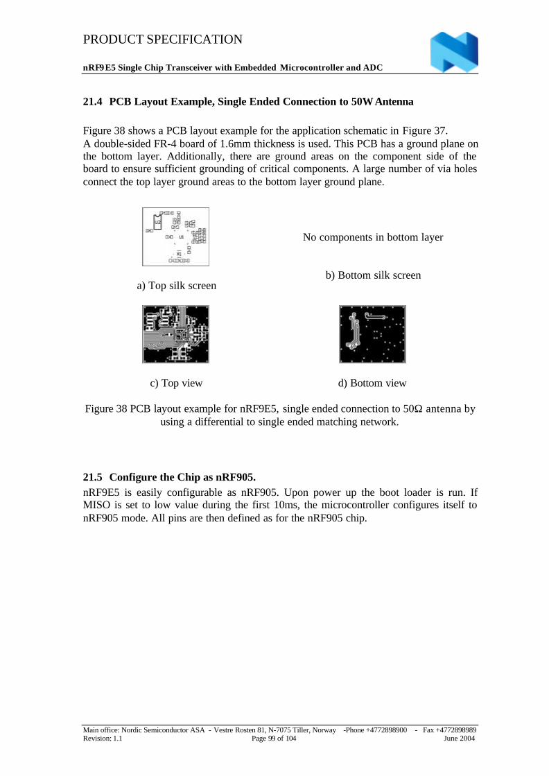
PRODUCT SPECIFICATION
nRF9E5 Single Chip Transceiver with Embedded Microcontroller and ADC
Main office: Nordic Semiconductor ASA - Vestre Rosten 81, N-7075 Tiller, Norway -Phone +4772898900 - Fax +4772898989Revision: 1.1 Page 99 of 104 June 2004
21.4 PCB Layout Example, Single Ended Connection to 50Ω Antenna
Figure 38 shows a PCB layout example for the application schematic in Figure 37.A double-sided FR-4 board of 1.6mm thickness is used. This PCB has a ground plane onthe bottom layer. Additionally, there are ground areas on the component side of theboard to ensure sufficient grounding of critical components. A large number of via holesconnect the top layer ground areas to the bottom layer ground plane.
a) Top silk screen
No components in bottom layer
b) Bottom silk screen
c) Top view d) Bottom view
Figure 38 PCB layout example for nRF9E5, single ended connection to 50Ω antenna byusing a differential to single ended matching network.
21.5 Configure the Chip as nRF905.nRF9E5 is easily configurable as nRF905. Upon power up the boot loader is run. IfMISO is set to low value during the first 10ms, the microcontroller configures itself tonRF905 mode. All pins are then defined as for the nRF905 chip.
PRODUCT SPECIFICATION
nRF9E5 Single Chip Transceiver with Embedded Microcontroller and ADC
Main office: Nordic Semiconductor ASA - Vestre Rosten 81, N-7075 Tiller, Norway -Phone +4772898900 - Fax +4772898989Revision: 1.1 Page 100 of 104 June 2004
22 ABSOLUTE MAXIMUM RATINGS
Supply VoltageVDD...............................- 0.3V to + 3.6VVSS ..................................................... 0V
Input VoltageVI ..........................- 0.3V to VDD + 0.3V
Output VoltageVO.........................- 0.3V to VDD + 0.3V
Total Power DissipationPD (TA=85°C)................................ 230mW
TemperaturesOperating temperature............................................ - 40°C to + 85°CStorage temperature...............................................- 40°C to + 125°C
Note: Stress exceeding one or more of the limiting values may cause permanent damageto the device.
ATTENTION!Electrostatic sensitive device.Observe precaution for handling.
PRODUCT SPECIFICATION
nRF9E5 Single Chip Transceiver with Embedded Microcontroller and ADC
Main office: Nordic Semiconductor ASA - Vestre Rosten 81, N-7075 Tiller, Norway -Phone +4772898900 - Fax +4772898989Revision: 1.1 Page 101 of 104 June 2004
23 GLOSSERY OF TERMS
Term DescriptionADC Analog to Digital ConverterAM Address MatchBOM Bill Of MaterialCD Carrier DetectCLK ClockCRC Cyclic Redundancy CheckCSN SPI Chip Select NotDR Data ReadyGFSK Gaussian Frequency Shift KeyingGPIO General Purpose Input OutputISM Industrial-Scientific-Medicalksps kilo Samples per SecondMCU Micro Controller UnitMISO SPI Master In Slave OutMOSI SPI Master Out Slave InPWM Pulse-Width ModulationPWR_DWN Power DownPWR_UP Power UpRAM Random Access MemoryROM Read Only MemoryRTC Real Time ClockRX ReceiveSCK SPI Serial ClockSPI Serial Programmable InterfaceSTBY StandbyTRX_EN Transmit/Receive EnableTX TransmitTX_EN Transmit EnableUART Universal Asynchronous Receiver TransmitterXTAL Crystal
Table 76 Glossary of terms.
PRODUCT SPECIFICATION
nRF9E5 Single Chip Transceiver with Embedded Microcontroller and ADC
Main office: Nordic Semiconductor ASA - Vestre Rosten 81, N-7075 Tiller, Norway -Phone +4772898900 - Fax +4772898989Revision: 1.1 Page 102 of 104 June 2004
24 DEFINITIONS
Data sheet statusObjective product specification This datasheet contains target specifications for product development.Preliminary productspecification
This datasheet contains preliminary data; supplementary data may bepublished from Nordic Semiconductor ASA later.
Product specification This datasheet contains final product specifications. Nordic SemiconductorASA reserves the right to make changes at any time without notice in order toimprove design and supply the best possible product.
Limiting valuesStress above one or more of the limiting values may cause permanent damage to the device. These are stressratings only and operation of the device at these or at any other conditions above those given in theSpecifications sections of the specification is not implied. Exposure to limiting values for extended periods mayaffect device reliability.Application informationWhere application information is given, it is advisory and does not form part of the specification.
Table 77 Definitions.
Nordic Semiconductor ASA reserves the right to make changes without further notice tothe product to improve reliability, function or design. Nordic Semiconductor does notassume any liability arising out of the application or use of any product or circuitsdescribed herein.
LIFE SUPPORT APPLICATIONSThese products are not designed for use in life support appliances, devices, or systemswhere malfunction of these products can reasonably be expected to result in personalinjury. Nordic Semiconductor ASA customers using or selling these products for use insuch applications do so at their own risk and agree to fully indemnify NordicSemiconductorSemiconductor ASA for any damages resulting from such improper useor sale.
Product specification revision date: 8.06.2004Datasheet order code: 080604nRF9E5
All rights reserved ®. Reproduction in whole or in part is prohibited without the priorwritten permission of the copyright holder.
PRODUCT SPECIFICATION
nRF9E5 Single Chip Transceiver with Embedded Microcontroller and ADC
Main office: Nordic Semiconductor ASA - Vestre Rosten 81, N-7075 Tiller, Norway -Phone +4772898900 - Fax +4772898989Revision: 1.1 Page 103 of 104 June 2004
25 YOUR NOTES
PRODUCT SPECIFICATION
nRF9E5 Single Chip Transceiver with Embedded Microcontroller and ADC
Main office: Nordic Semiconductor ASA - Vestre Rosten 81, N-7075 Tiller, Norway -Phone +4772898900 - Fax +4772898989Revision: 1.1 Page 104 of 104 June 2004
Nordic Semiconductor ASA – World Wide Distributors
For Your nearest dealer, please see http://www.nordicsemi.no
Main Office:Vestre Rosten 81, N-7075 Tiller, Norway
Phone: +47 72 89 89 00, Fax: +47 72 89 89 89
Visit the Nordic Semiconductor ASA website at http://www.nordicsemi.no