450 na, 9 khz op amp - microchip technologyww1.microchip.com/downloads/en/devicedoc/22257c.pdf ·...
TRANSCRIPT
MCP6441/2/4450 nA, 9 kHz Op Amp
Features:• Low Quiescent Current: 450 nA (typical)• Gain Bandwidth Product: 9 kHz (typical)• Supply Voltage Range: 1.4V to 6.0V• Rail-to-Rail Input and Output• Unity Gain Stable• Slew Rate: 3V/ms (typical)• Extended Temperature Range: -40°C to +125°C• No Phase Reversal• Small Packages
Applications:• Portable Equipment• Battery Powered System• Data Acquisition Equipment• Sensor Conditioning• Battery Current Sensing• Analog Active Filters
Design Aids:• SPICE Macro Models • FilterLab® Software• Microchip Advanced Part Selector (MAPS)• Analog Demonstration and Evaluation Boards• Application Notes
Description:The MCP6441/2/4 device is a single nanopoweroperational amplifier (op amp), which has lowquiescent current (450 nA, typical) and rail-to-rail inputand output operation. This op amp is unity gain stableand has a gain bandwidth product of 9 kHz (typical).These devices operate with a single supply voltage aslow as 1.4V. These features make the family of opamps well suited for single-supply, battery-poweredapplications.
The MCP6441/2/4 op amp is designed with Microchip’sadvanced CMOS process and offered in single(MCP6441), dual (MCP6442), and quad (MCP6444)configurations. All devices are available in theextended temperature range, with a power supplyrange of 1.4V to 6.0V.
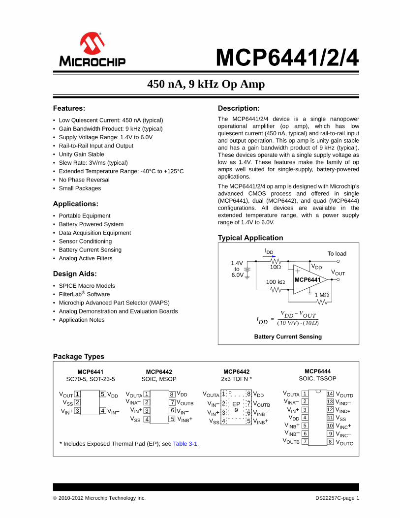
Typical Application
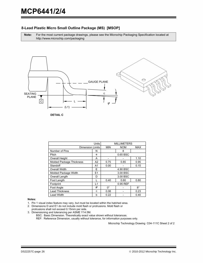
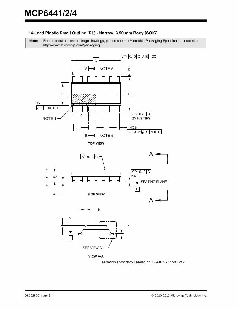
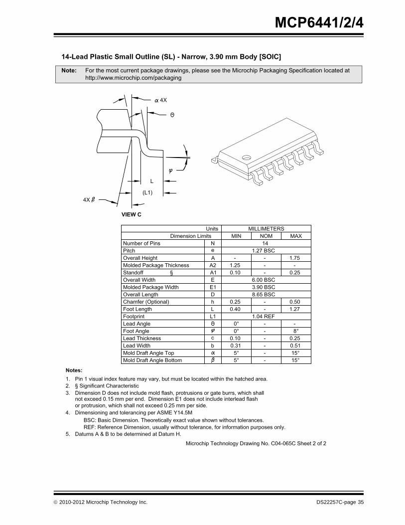
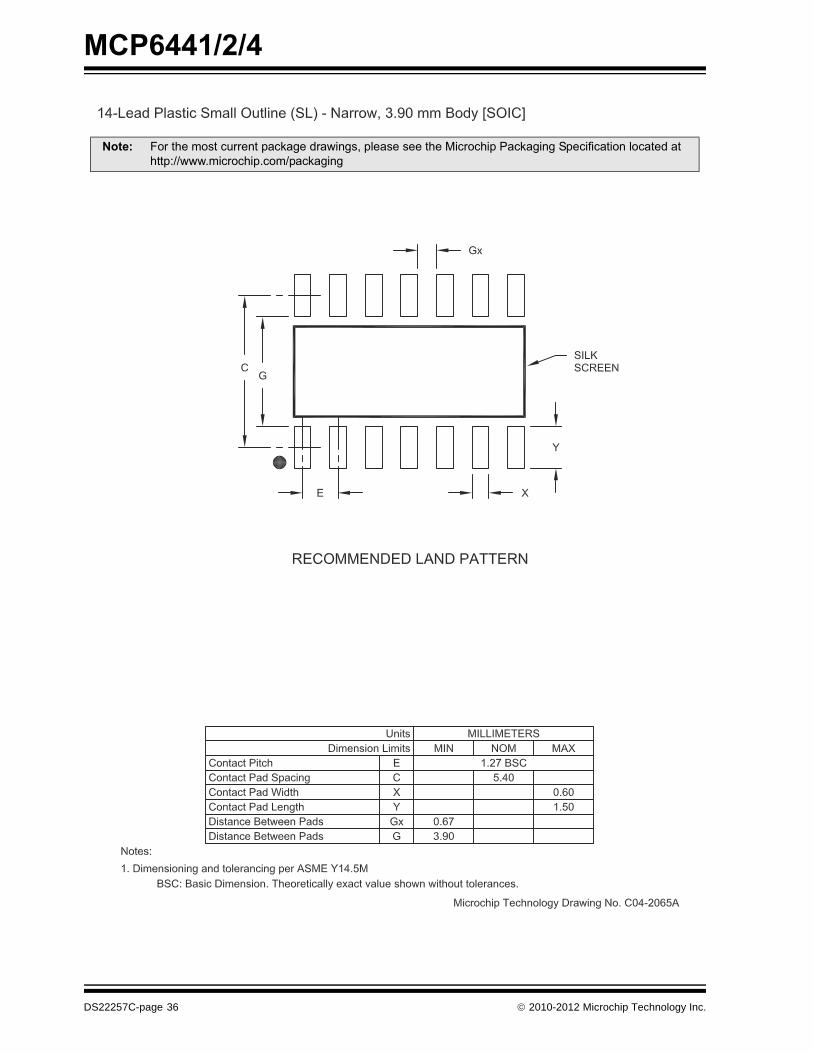
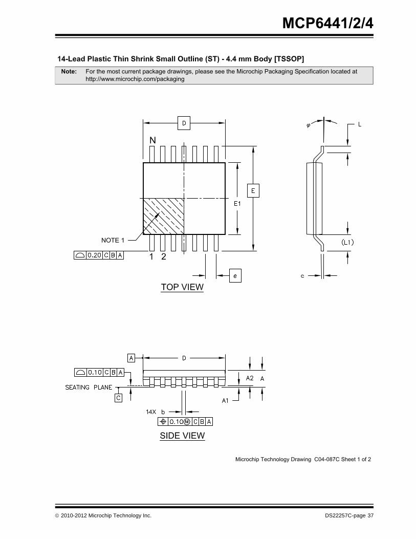
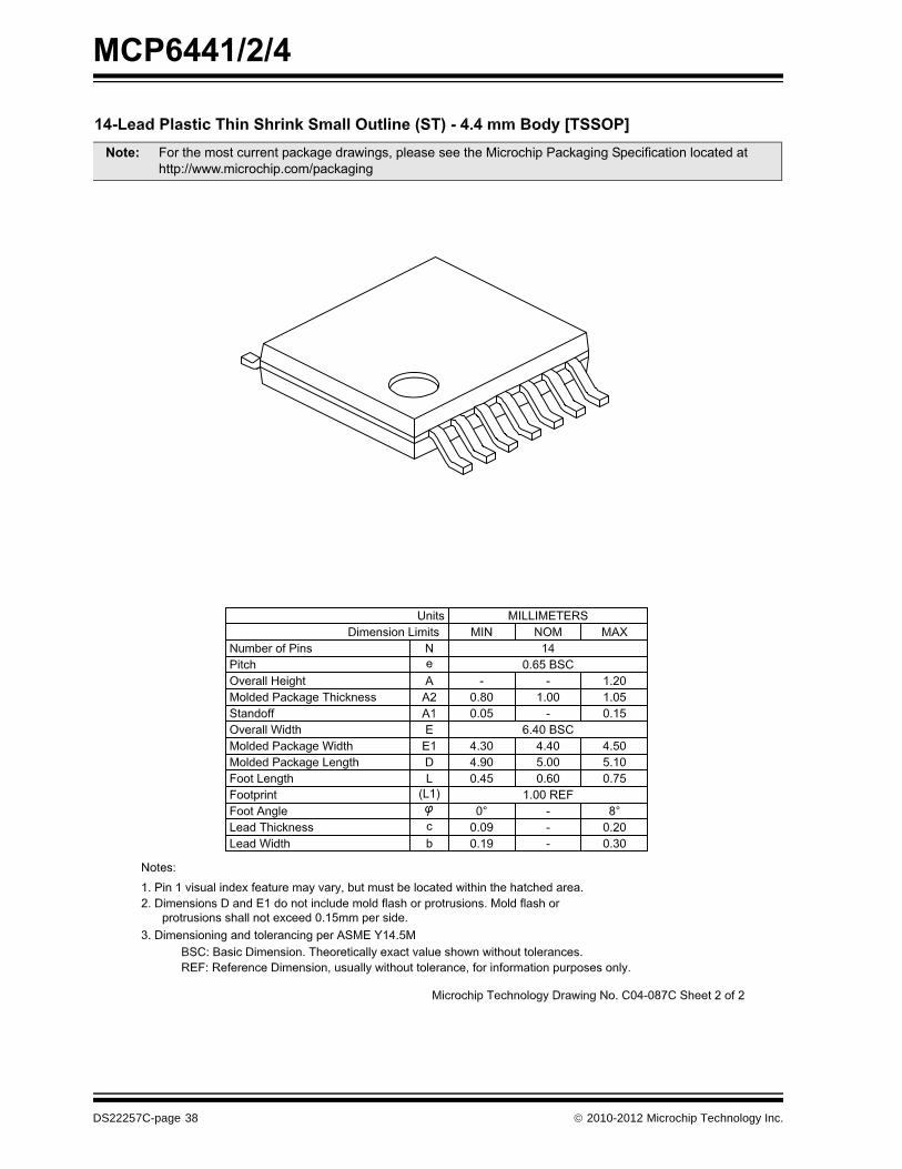
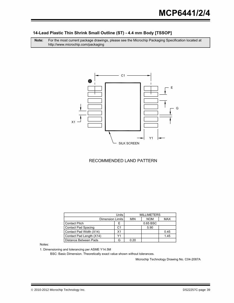
Package Types
VDD
IDD
100 kΩ
1 MΩ
1.4VVOUT
Battery Current Sensing
10Ωto6.0V
IDDVDD VOUT–
10 V/V( ) 10Ω( )⋅------------------------------------------=
To load
MCP6441
5
4
123
VDD
VIN–VIN+VSS
VOUT
MCP6441SC70-5, SOT-23-5
5
123
VDD
VIN–VIN+VSS
VOUTA
MCP6442SOIC, MSOP
MCP6444SOIC, TSSOP
8 76
VOUTB
4 VINB+
VINA–
5
123
VDD
VIND+VIN+VSS
VOUTA
8 76
VOUTC
4VINB+
VINA–
9 10
14
12 11
13
VINB–VOUTB
VINC–VINC+
VIND–VOUTD
MCP64422x3 TDFN *
VIN+VIN–
VSS
VOUTBVINB–
1
234
8
765 VINB+
VDDVOUTA
EP9
* Includes Exposed Thermal Pad (EP); see Table 3-1.
© 2010-2012 Microchip Technology Inc. DS22257C-page 1

MCP6441/2/4
NOTES:DS22257C-page 2 © 2010-2012 Microchip Technology Inc.
MCP6441/2/4
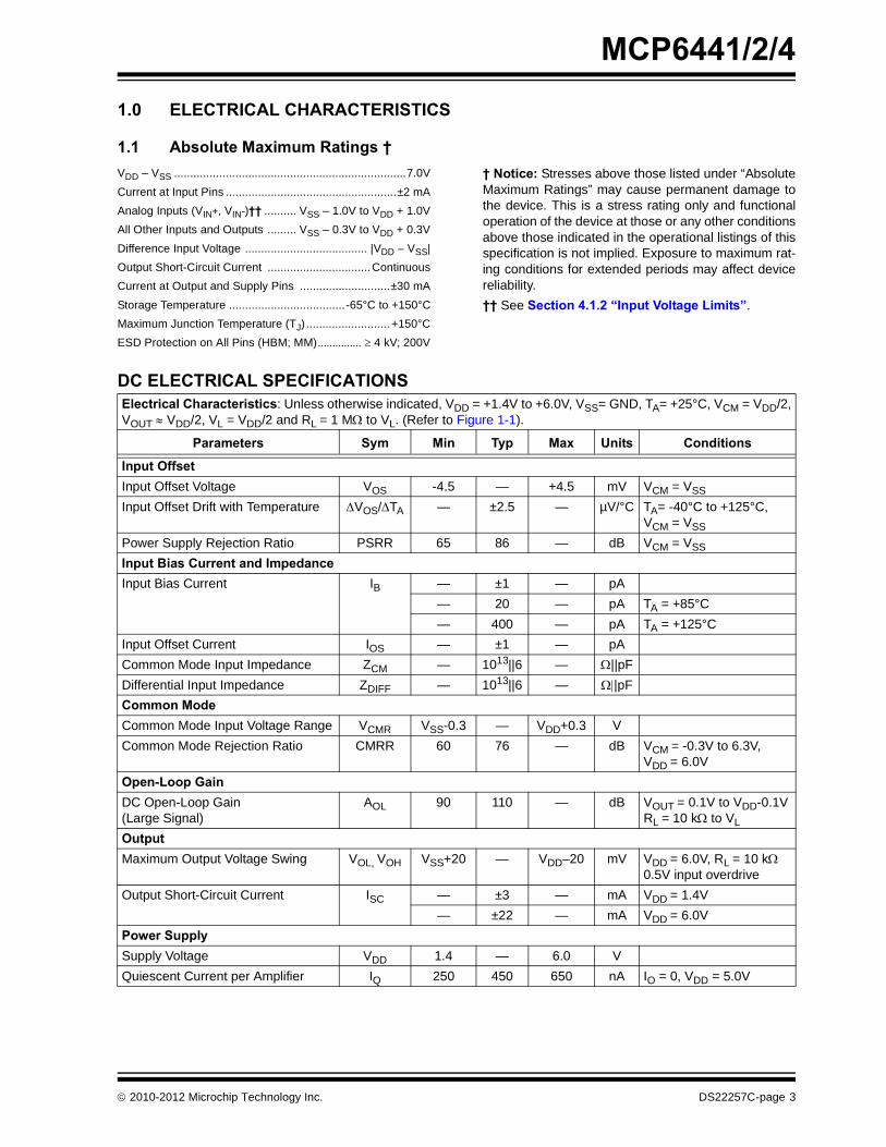
1.0 ELECTRICAL CHARACTERISTICS
1.1 Absolute Maximum Ratings †VDD – VSS ........................................................................7.0VCurrent at Input Pins .....................................................±2 mAAnalog Inputs (VIN+, VIN-)†† .......... VSS – 1.0V to VDD + 1.0VAll Other Inputs and Outputs ......... VSS – 0.3V to VDD + 0.3VDifference Input Voltage ...................................... |VDD – VSS|Output Short-Circuit Current ................................ContinuousCurrent at Output and Supply Pins ............................±30 mAStorage Temperature ....................................-65°C to +150°CMaximum Junction Temperature (TJ) .......................... +150°CESD Protection on All Pins (HBM; MM) ............... ≥ 4 kV; 200V
† Notice: Stresses above those listed under “AbsoluteMaximum Ratings” may cause permanent damage tothe device. This is a stress rating only and functionaloperation of the device at those or any other conditionsabove those indicated in the operational listings of thisspecification is not implied. Exposure to maximum rat-ing conditions for extended periods may affect devicereliability.†† See Section 4.1.2 “Input Voltage Limits”.
DC ELECTRICAL SPECIFICATIONSElectrical Characteristics: Unless otherwise indicated, VDD = +1.4V to +6.0V, VSS= GND, TA= +25°C, VCM = VDD/2,VOUT ≈ VDD/2, VL = VDD/2 and RL = 1 MΩ to VL. (Refer to Figure 1-1).
Parameters Sym Min Typ Max Units Conditions
Input OffsetInput Offset Voltage VOS -4.5 — +4.5 mV VCM = VSSInput Offset Drift with Temperature ΔVOS/ΔTA — ±2.5 — µV/°C TA= -40°C to +125°C,
VCM = VSSPower Supply Rejection Ratio PSRR 65 86 — dB VCM = VSSInput Bias Current and ImpedanceInput Bias Current IB — ±1 — pA
— 20 — pA TA = +85°C— 400 — pA TA = +125°C
Input Offset Current IOS — ±1 — pACommon Mode Input Impedance ZCM — 1013||6 — Ω||pFDifferential Input Impedance ZDIFF — 1013||6 — Ω||pFCommon ModeCommon Mode Input Voltage Range VCMR VSS-0.3 — VDD+0.3 VCommon Mode Rejection Ratio CMRR 60 76 — dB VCM = -0.3V to 6.3V,
VDD = 6.0VOpen-Loop GainDC Open-Loop Gain(Large Signal)
AOL 90 110 — dB VOUT = 0.1V to VDD-0.1VRL = 10 kΩ to VL
OutputMaximum Output Voltage Swing VOL, VOH VSS+20 — VDD–20 mV VDD = 6.0V, RL = 10 kΩ
0.5V input overdriveOutput Short-Circuit Current ISC — ±3 — mA VDD = 1.4V
— ±22 — mA VDD = 6.0VPower SupplySupply Voltage VDD 1.4 — 6.0 VQuiescent Current per Amplifier IQ 250 450 650 nA IO = 0, VDD = 5.0V
© 2010-2012 Microchip Technology Inc. DS22257C-page 3
MCP6441/2/4
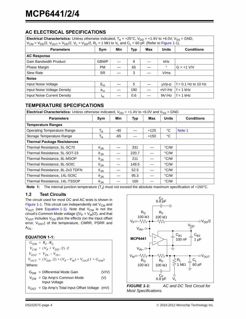
1.2 Test CircuitsThe circuit used for most DC and AC tests is shown inFigure 1-1. This circuit can independently set VCM andVOUT (see Equation 1-1). Note that VCM is not thecircuit’s Common Mode voltage ((VP + VM)/2), and thatVOST includes VOS plus the effects (on the input offseterror, VOST) of the temperature, CMRR, PSRR andAOL.
EQUATION 1-1:
FIGURE 1-1: AC and DC Test Circuit for Most Specifications.
AC ELECTRICAL SPECIFICATIONS Electrical Characteristics: Unless otherwise indicated, TA = +25°C, VDD = +1.4V to +6.0V, VSS = GND, VCM = VDD/2, VOUT ≈ VDD/2, VL = VDD/2, RL = 1 MΩ to VL and CL = 60 pF. (Refer to Figure 1-1).
Parameters Sym Min Typ Max Units Conditions
AC ResponseGain Bandwidth Product GBWP — 9 — kHzPhase Margin PM — 65 — ° G = +1 V/VSlew Rate SR — 3 — V/msNoiseInput Noise Voltage Eni — 5 — µVp-p f = 0.1 Hz to 10 HzInput Noise Voltage Density eni — 190 — nV/√Hz f = 1 kHzInput Noise Current Density ini — 0.6 — fA/√Hz f = 1 kHz
TEMPERATURE SPECIFICATIONSElectrical Characteristics: Unless otherwise indicated, VDD = +1.4V to +6.0V and VSS = GND.
Parameters Sym Min Typ Max Units Conditions
Temperature RangesOperating Temperature Range TA -40 — +125 °C Note 1Storage Temperature Range TA -65 — +150 °CThermal Package ResistancesThermal Resistance, 5L-SC70 θJA — 331 — °C/WThermal Resistance, 5L-SOT-23 θJA — 220.7 — °C/WThermal Resistance, 8L-MSOP θJA — 211 — °C/WThermal Resistance, 8L-SOIC θJA — 149.5 — °C/WThermal Resistance, 8L-2x3 TDFN θJA — 52.5 — °C/WThermal Resistance, 14L-SOIC θJA — 95.3 — °C/WThermal Resistance, 14L-TSSOP θJA — 100 — °C/WNote 1: The internal junction temperature (TJ) must not exceed the absolute maximum specification of +150°C.
GDM RF RG⁄=VCM VP VDD 2⁄+( ) 2⁄=
VOUT VDD 2⁄( ) VP VM–( ) VOST 1 GDM+( )+ +=Where:
GDM = Differential Mode Gain (V/V)VCM = Op Amp’s Common Mode
Input Voltage(V)
VOST = Op Amp’s Total Input Offset Voltage (mV)
VOST VIN– VIN+–=
VDD
RG RF
VOUTVM
CB2
CLRL
VL
CB1
100 kΩ100 kΩ
RG RF
VDD/2VP
100 kΩ100 kΩ
60 pF1 MΩ
1 µF100 nF
VIN–
VIN+
CF6.8 pF
CF6.8 pF
MCP6441
DS22257C-page 4 © 2010-2012 Microchip Technology Inc.
MCP6441/2/4
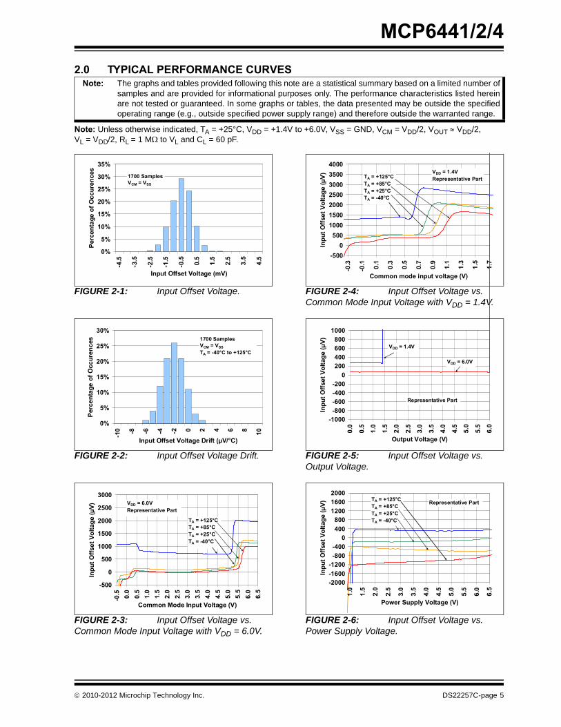
2.0 TYPICAL PERFORMANCE CURVES
Note: Unless otherwise indicated, TA = +25°C, VDD = +1.4V to +6.0V, VSS = GND, VCM = VDD/2, VOUT ≈ VDD/2,VL = VDD/2, RL = 1 MΩ to VL and CL = 60 pF.
FIGURE 2-1: Input Offset Voltage.
FIGURE 2-2: Input Offset Voltage Drift.
FIGURE 2-3: Input Offset Voltage vs. Common Mode Input Voltage with VDD = 6.0V.
FIGURE 2-4: Input Offset Voltage vs. Common Mode Input Voltage with VDD = 1.4V.
FIGURE 2-5: Input Offset Voltage vs. Output Voltage.
FIGURE 2-6: Input Offset Voltage vs. Power Supply Voltage.
Note: The graphs and tables provided following this note are a statistical summary based on a limited number ofsamples and are provided for informational purposes only. The performance characteristics listed hereinare not tested or guaranteed. In some graphs or tables, the data presented may be outside the specifiedoperating range (e.g., outside specified power supply range) and therefore outside the warranted range.
0%
5%
10%
15%
20%
25%
30%
35%
-4.5
-3.5
-2.5
-1.5
-0.5 0.5
1.5
2.5
3.5
4.5
Input Offset Voltage (mV)
Perc
enta
ge o
f Occ
uren
ces
1700 SamplesVCM = VSS
0%
5%
10%
15%
20%
25%
30%
-10 -8 -6 -4 -2 0 2 4 6 8 10
Input Offset Voltage Drift (µV/°C)
Perc
enta
ge o
f Occ
uren
ces 1700 Samples
VCM = VSSTA = -40°C to +125°C
-500
0
500
1000
1500
2000
2500
3000
-0.5 0.0
0.5
1.0
1.5
2.0
2.5
3.0
3.5
4.0
4.5
5.0
5.5
6.0
6.5
Common Mode Input Voltage (V)
Inpu
t Offs
et V
olta
ge (µ
V) VDD = 6.0VRepresentative Part
TA = +125°CTA = +85°CTA = +25°CTA = -40°C
-5000
5001000150020002500300035004000
-0.3
-0.1 0.1
0.3
0.5
0.7
0.9
1.1
1.3
1.5
1.7
Common mode input voltage (V)
Inpu
t Offs
et V
olta
ge (µ
V)
VDD = 1.4VRepresentative PartTA = +125°C
TA = +85°CTA = +25°CTA = -40°C
-1000-800-600-400-200
0200400600800
1000
0.0
0.5
1.0
1.5
2.0
2.5
3.0
3.5
4.0
4.5
5.0
5.5
6.0
Output Voltage (V)
Inpu
t Offs
et V
olta
ge (µ
V)
VDD = 6.0V
VDD = 1.4V
Representative Part
-2000-1600-1200-800-400
0400800
120016002000
1.0
1.5
2.0
2.5
3.0
3.5
4.0
4.5
5.0
5.5
6.0
6.5
Power Supply Voltage (V)
Inpu
t Offs
et V
olta
ge (µ
V) Representative PartTA = +125°CTA = +85°CTA = +25°CTA = -40°C
© 2010-2012 Microchip Technology Inc. DS22257C-page 5
MCP6441/2/4
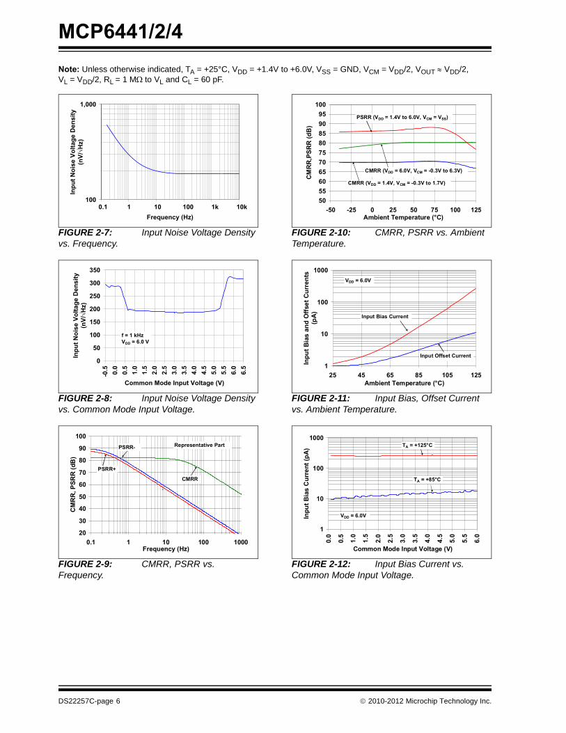
Note: Unless otherwise indicated, TA = +25°C, VDD = +1.4V to +6.0V, VSS = GND, VCM = VDD/2, VOUT ≈ VDD/2,VL = VDD/2, RL = 1 MΩ to VL and CL = 60 pF.FIGURE 2-7: Input Noise Voltage Density vs. Frequency.
FIGURE 2-8: Input Noise Voltage Density vs. Common Mode Input Voltage.
FIGURE 2-9: CMRR, PSRR vs. Frequency.
FIGURE 2-10: CMRR, PSRR vs. Ambient Temperature.
FIGURE 2-11: Input Bias, Offset Current vs. Ambient Temperature.
FIGURE 2-12: Input Bias Current vs. Common Mode Input Voltage.
100
1,000
0.1 1 10 100 1000 10000Frequency (Hz)
Inpu
t Noi
se V
olta
ge D
ensi
ty
(nV/
Hz)
0.1 1 10 100 1k 10k
0
50
100
150
200
250
300
350
-0.5 0.0
0.5
1.0
1.5
2.0
2.5
3.0
3.5
4.0
4.5
5.0
5.5
6.0
6.5
Common Mode Input Voltage (V)
Inpu
t Noi
se V
olta
ge D
ensi
ty
(nV/
Hz)
f = 1 kHzVDD = 6.0 V
20
30
40
50
60
70
80
90
100
0.1 1 10 100 1000Frequency (Hz)
CM
RR
, PSR
R (d
B)
CMRR
PSRR-
PSRR+
c
Representative Part
50556065707580859095
100
-50 -25 0 25 50 75 100 125Ambient Temperature (°C)
CM
RR
,PSR
R (d
B)
PSRR (VDD = 1.4V to 6.0V, VCM = VSS)
CMRR (VDD = 6.0V, VCM = -0.3V to 6.3V)
CMRR (VDD = 1.4V, VCM = -0.3V to 1.7V)
1
10
100
1000
25 45 65 85 105 125Ambient Temperature (°C)
Inpu
t Bia
s an
d O
ffset
Cur
rent
s (p
A)
Input Bias Current
VDD = 6.0V
Input Offset Current
1
10
100
1000
0.0
0.5
1.0
1.5
2.0
2.5
3.0
3.5
4.0
4.5
5.0
5.5
6.0
Common Mode Input Voltage (V)
Inpu
t Bia
s C
urre
nt (p
A)
VDD = 6.0V
TA = +125°C
TA = +85°C
DS22257C-page 6 © 2010-2012 Microchip Technology Inc.
MCP6441/2/4
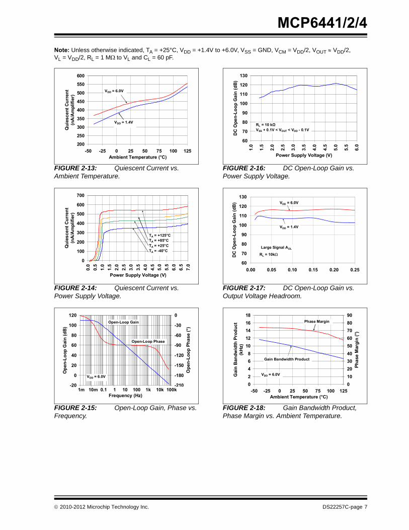
Note: Unless otherwise indicated, TA = +25°C, VDD = +1.4V to +6.0V, VSS = GND, VCM = VDD/2, VOUT ≈ VDD/2,VL = VDD/2, RL = 1 MΩ to VL and CL = 60 pF.FIGURE 2-13: Quiescent Current vs. Ambient Temperature.
FIGURE 2-14: Quiescent Current vs. Power Supply Voltage.
FIGURE 2-15: Open-Loop Gain, Phase vs. Frequency.
FIGURE 2-16: DC Open-Loop Gain vs. Power Supply Voltage.
FIGURE 2-17: DC Open-Loop Gain vs. Output Voltage Headroom.
FIGURE 2-18: Gain Bandwidth Product, Phase Margin vs. Ambient Temperature.
200
250
300
350
400
450
500
550
600
-50 -25 0 25 50 75 100 125Ambient Temperature (°C)
Qui
esce
nt C
urre
nt
(nA
/Am
plifi
er)
VDD = 6.0V
VDD = 1.4V
0
100
200
300
400
500
600
700
0.0
0.5
1.0
1.5
2.0
2.5
3.0
3.5
4.0
4.5
5.0
5.5
6.0
6.5
7.0
Power Supply Voltage (V)
Qui
esce
nt C
urre
nt
(nA
/Am
plifi
er)
TA = +125°CTA = +85°CTA = +25°CTA = -40°C
-20
0
20
40
60
80
100
120
1.0E-03 1.0E-02 1.0E-01 1.0E+00 1.0E+01 1.0E+02 1.0E+03 1.0E+04 1.0E+05
Frequency (Hz)
Ope
n-Lo
op G
ain
(dB
)
-210
-180
-150
-120
-90
-60
-30
0
Ope
n-Lo
op P
hase
(°)
Open-Loop Gain
Open-Loop Phase
VDD = 6.0V
1m 10m 0.1 1 10 100 1k 10k 100k
60
70
80
90
100
110
120
130
1.0
1.5
2.0
2.5
3.0
3.5
4.0
4.5
5.0
5.5
6.0
Power Supply Voltage (V)
DC
Ope
n-Lo
op G
ain
(dB
)
RL = 10 kΩVSS + 0.1V < VOUT < VDD - 0.1V
120
130
B) VDD = 6.0V
110
120
ain
(dB DD
100
oop
Ga
VDD = 1.4V
80
90O
pen-
Lo
L Si l A70D
CO
RL = 10k
Large Signal AOL
600.00 0.05 0.10 0.15 0.20 0.25
02468
1012141618
-50 -25 0 25 50 75 100 125Ambient Temperature (°C)
Gai
n B
andw
idth
Pro
duct
(k
Hz)
0102030405060708090
Phas
e M
argi
n (°
)Gain Bandwidth Product
Phase Margin
VDD = 6.0V
© 2010-2012 Microchip Technology Inc. DS22257C-page 7
MCP6441/2/4
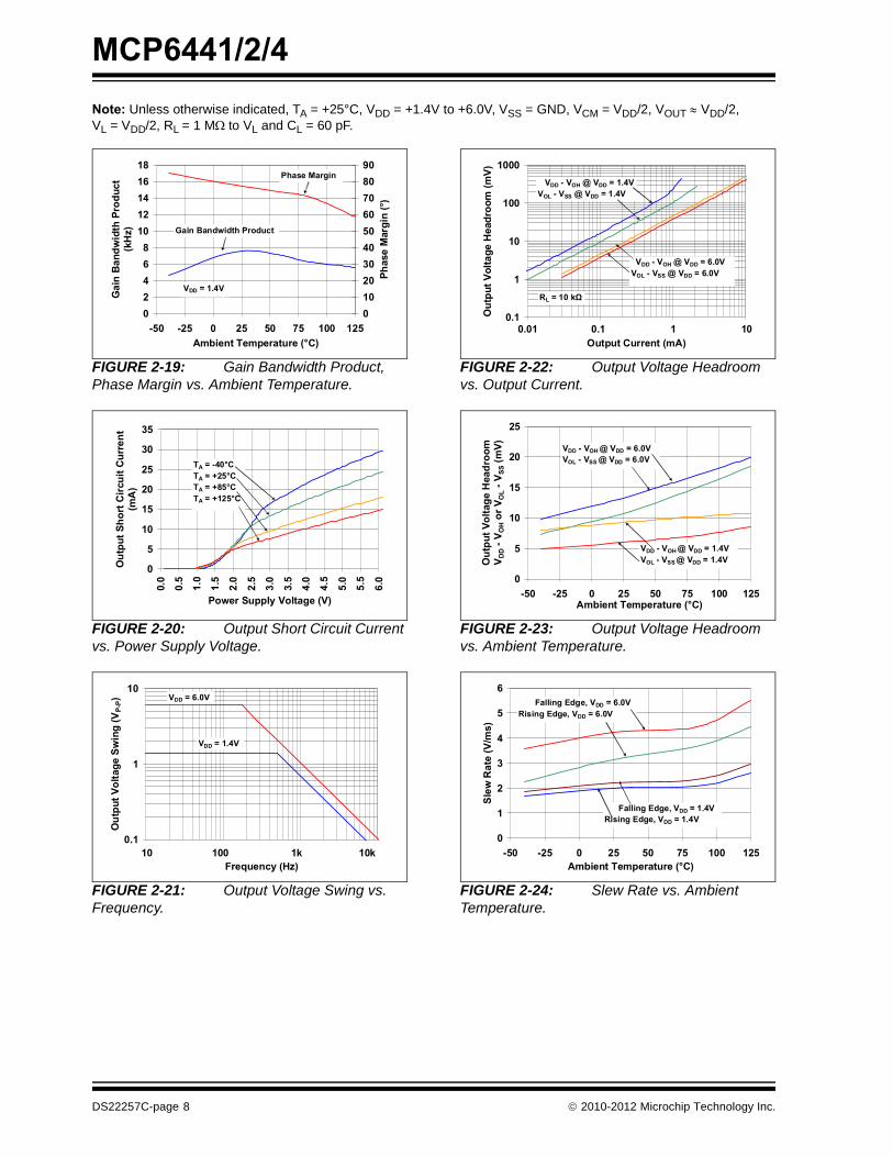
Note: Unless otherwise indicated, TA = +25°C, VDD = +1.4V to +6.0V, VSS = GND, VCM = VDD/2, VOUT ≈ VDD/2,VL = VDD/2, RL = 1 MΩ to VL and CL = 60 pF.FIGURE 2-19: Gain Bandwidth Product, Phase Margin vs. Ambient Temperature.
FIGURE 2-20: Output Short Circuit Current vs. Power Supply Voltage.
FIGURE 2-21: Output Voltage Swing vs. Frequency.
FIGURE 2-22: Output Voltage Headroom vs. Output Current.
FIGURE 2-23: Output Voltage Headroom vs. Ambient Temperature.
FIGURE 2-24: Slew Rate vs. Ambient Temperature.
02468
1012141618
-50 -25 0 25 50 75 100 125Ambient Temperature (°C)
Gai
n B
andw
idth
Pro
duct
(k
Hz)
0102030405060708090
Phas
e M
argi
n (°
)
Gain Bandwidth Product
Phase Margin
VDD = 1.4V
0
5
10
15
20
25
30
35
0.0
0.5
1.0
1.5
2.0
2.5
3.0
3.5
4.0
4.5
5.0
5.5
6.0
Power Supply Voltage (V)
Out
put S
hort
Circ
uit C
urre
nt
(mA
)
TA = -40°CTA = +25°CTA = +85°CTA = +125°C
0.1
1
10
10 100 1000 10000Frequency (Hz)
Out
put V
olta
ge S
win
g (V
P-P)
VDD = 1.4V
VDD = 6.0V
10 100 1k 10k
0.1
1
10
100
1000
10 100 1000 10000Output Current (mA)
Out
put V
olta
ge H
eadr
oom
(mV)
VDD - VOH @ VDD = 1.4VVOL - VSS @ VDD = 1.4V
VDD - VOH @ VDD = 6.0VVOL - VSS @ VDD = 6.0V
RL = 10 kΩ
0.01 0.1 1 10
0
5
10
15
20
25
-50 -25 0 25 50 75 100 125Ambient Temperature (°C)
Out
put V
olta
ge H
eadr
oom
V DD
- VO
H or
VO
L - V
SS (m
V)
VDD - VOH @ VDD = 1.4VVOL - VSS @ VDD = 1.4V
VDD - VOH @ VDD = 6.0VVOL - VSS @ VDD = 6.0V
0
1
2
3
4
5
6
-50 -25 0 25 50 75 100 125Ambient Temperature (°C)
Slew
Rat
e (V
/ms)
Falling Edge, VDD = 6.0VRising Edge, VDD = 6.0V
Falling Edge, VDD = 1.4VRising Edge, VDD = 1.4V
DS22257C-page 8 © 2010-2012 Microchip Technology Inc.
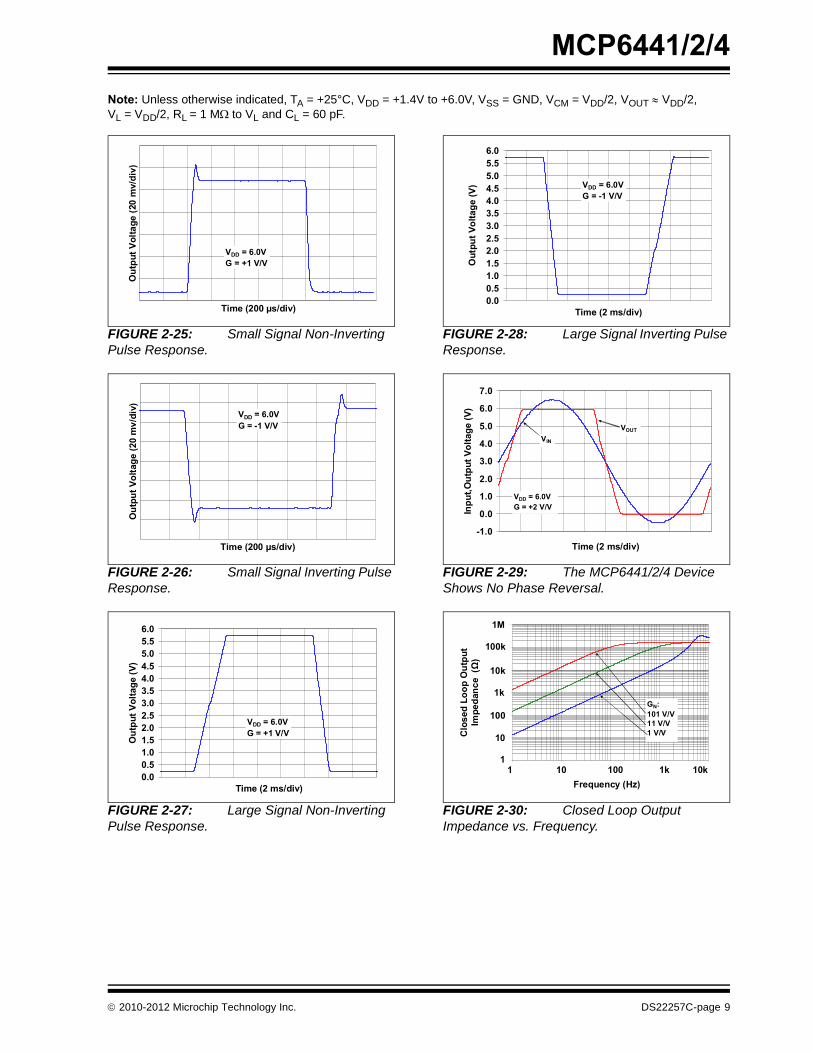
MCP6441/2/4
Note: Unless otherwise indicated, TA = +25°C, VDD = +1.4V to +6.0V, VSS = GND, VCM = VDD/2, VOUT ≈ VDD/2,VL = VDD/2, RL = 1 MΩ to VL and CL = 60 pF.FIGURE 2-25: Small Signal Non-Inverting Pulse Response.
FIGURE 2-26: Small Signal Inverting Pulse Response.
FIGURE 2-27: Large Signal Non-Inverting Pulse Response.
FIGURE 2-28: Large Signal Inverting Pulse Response.
FIGURE 2-29: The MCP6441/2/4 Device Shows No Phase Reversal.
FIGURE 2-30: Closed Loop Output Impedance vs. Frequency.
Time (200 µs/div)
Out
put V
olta
ge (2
0 m
v/di
v)
VDD = 6.0VG = +1 V/V
Time (200 µs/div)
Out
put V
olta
ge (2
0 m
v/di
v)
VDD = 6.0VG = -1 V/V
0.00.51.01.52.02.53.03.54.04.55.05.56.0
Time (2 ms/div)
Out
put V
olta
ge (V
)
VDD = 6.0VG = +1 V/V
0.00.51.01.52.02.53.03.54.04.55.05.56.0
Time (2 ms/div)
Out
put V
olta
ge (V
) VDD = 6.0VG = -1 V/V
-1.0
0.0
1.0
2.0
3.0
4.0
5.0
6.0
7.0
Time (2 ms/div)
Inpu
t,Out
put V
olta
ge (V
)
VDD = 6.0VG = +2 V/V
VOUT
VIN
1
10
100
1000
10000
100000
1000000
1 10 100 1000 10000
Frequency (Hz)
Clo
sed
Loop
Out
put
Impe
danc
e (Ω
)
1 10 100 1k 10k 1
10
100
1k
10k
100k
1M
GN:101 V/V11 V/V1 V/V
© 2010-2012 Microchip Technology Inc. DS22257C-page 9
MCP6441/2/4
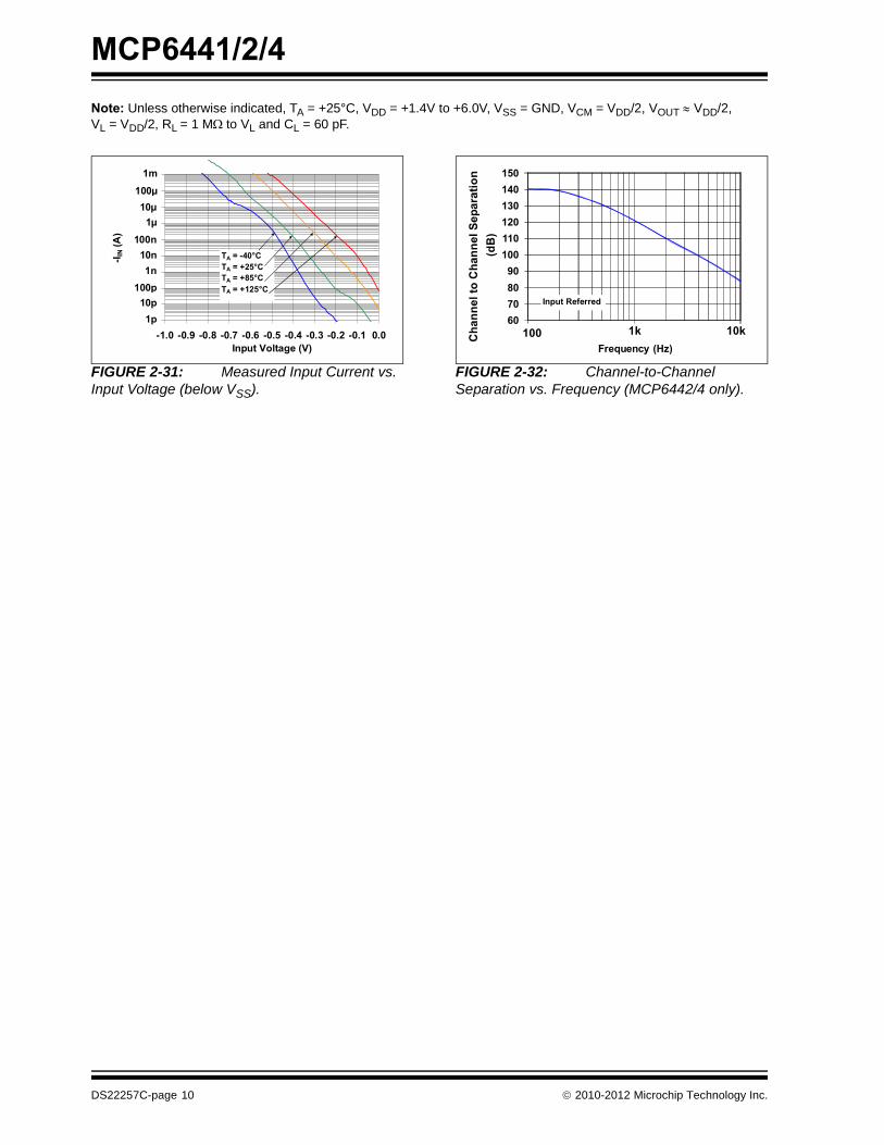
Note: Unless otherwise indicated, TA = +25°C, VDD = +1.4V to +6.0V, VSS = GND, VCM = VDD/2, VOUT ≈ VDD/2,VL = VDD/2, RL = 1 MΩ to VL and CL = 60 pF.FIGURE 2-31: Measured Input Current vs. Input Voltage (below VSS).
FIGURE 2-32: Channel-to-Channel Separation vs. Frequency (MCP6442/4 only).
1.E-121.E-111.E-101.E-091.E-081.E-071.E-061.E-051.E-041.E-03
-1.0 -0.9 -0.8 -0.7 -0.6 -0.5 -0.4 -0.3 -0.2 -0.1 0.0Input Voltage (V)
-I IN
(A)
1m100µ10µ
1µ100n
10n1n
100p10p1p
TA = -40°CTA = +25°CTA = +85°CTA = +125°C
60708090
100110120130140150
100 1000 10000Channel to Channel Separation
(dB)
Frequency (Hz)100 1k
Input Referred
Cha
nnel
to C
hann
el S
epar
atio
n(d
B)
1k100 10k
DS22257C-page 10 © 2010-2012 Microchip Technology Inc.
MCP6441/2/4
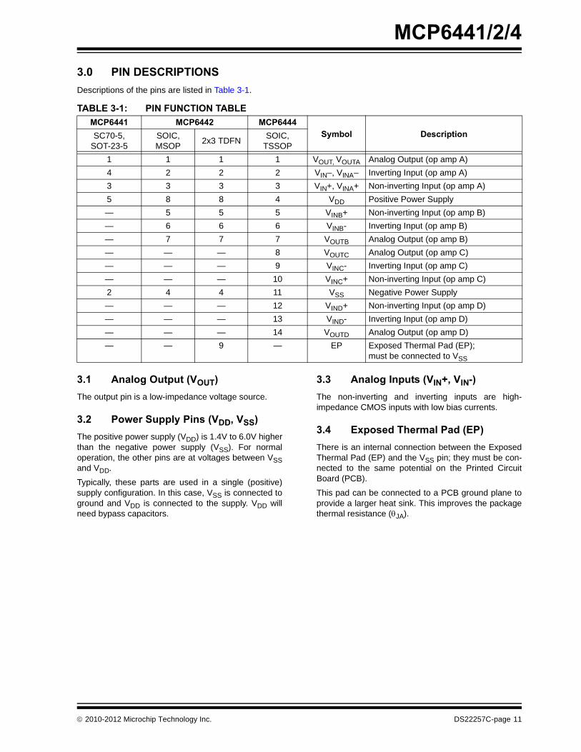
3.0 PIN DESCRIPTIONSDescriptions of the pins are listed in Table 3-1.
3.1 Analog Output (VOUT)The output pin is a low-impedance voltage source.
3.2 Power Supply Pins (VDD, VSS)The positive power supply (VDD) is 1.4V to 6.0V higherthan the negative power supply (VSS). For normaloperation, the other pins are at voltages between VSSand VDD.
Typically, these parts are used in a single (positive)supply configuration. In this case, VSS is connected toground and VDD is connected to the supply. VDD willneed bypass capacitors.
3.3 Analog Inputs (VIN+, VIN-)The non-inverting and inverting inputs are high-impedance CMOS inputs with low bias currents.
3.4 Exposed Thermal Pad (EP)There is an internal connection between the ExposedThermal Pad (EP) and the VSS pin; they must be con-nected to the same potential on the Printed CircuitBoard (PCB).
This pad can be connected to a PCB ground plane toprovide a larger heat sink. This improves the packagethermal resistance (θJA).
TABLE 3-1: PIN FUNCTION TABLEMCP6441 MCP6442 MCP6444
Symbol DescriptionSC70-5, SOT-23-5
SOIC, MSOP 2x3 TDFN SOIC,
TSSOP1 1 1 1 VOUT, VOUTA Analog Output (op amp A)4 2 2 2 VIN–, VINA– Inverting Input (op amp A)3 3 3 3 VIN+, VINA+ Non-inverting Input (op amp A)5 8 8 4 VDD Positive Power Supply— 5 5 5 VINB+ Non-inverting Input (op amp B)— 6 6 6 VINB- Inverting Input (op amp B)— 7 7 7 VOUTB Analog Output (op amp B)— — — 8 VOUTC Analog Output (op amp C)— — — 9 VINC- Inverting Input (op amp C)— — — 10 VINC+ Non-inverting Input (op amp C)2 4 4 11 VSS Negative Power Supply— — — 12 VIND+ Non-inverting Input (op amp D)— — — 13 VIND- Inverting Input (op amp D)— — — 14 VOUTD Analog Output (op amp D)— — 9 — EP Exposed Thermal Pad (EP);
must be connected to VSS
© 2010-2012 Microchip Technology Inc. DS22257C-page 11
MCP6441/2/4
Notes:DS22257C-page 12 © 2010-2012 Microchip Technology Inc.
MCP6441/2/4
4.0 APPLICATION INFORMATIONThe MCP6441/2/4 op amp is manufactured usingMicrochip’s state-of-the-art CMOS process, specificallydesigned for low power applications.
4.1 Rail-to-Rail Input
4.1.1 PHASE REVERSALThe MCP6441/2/4 op amp is designed to preventphase reversal, when the input pins exceed the supplyvoltages. Figure 2-29 shows the input voltageexceeding the supply voltage with no phase reversal.
4.1.2 INPUT VOLTAGE LIMITSIn order to prevent damage and/or improper operationof the amplifier, the circuit must limit the voltages at theinput pins (see Section 1.1, Absolute MaximumRatings †).
The Electrostatic Discharge (ESD) protection on theinputs can be depicted as shown in Figure 4-1. Thisstructure was chosen to protect the input transistorsagainst many, but not all, over-voltage conditions, andto minimize the input bias current (IB).
FIGURE 4-1: Simplified Analog Input ESD Structures.The input ESD diodes clamp the inputs when they tryto go more than one diode drop below VSS. They alsoclamp any voltages that go well above VDD; theirbreakdown voltage is high enough to allow normaloperation, but not low enough to protect against slowover-voltage (beyond VDD) events. Very fast ESDevents that meet the spec are limited so that damagedoes not occur.
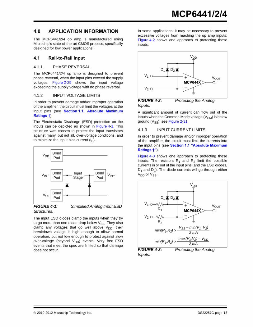
In some applications, it may be necessary to preventexcessive voltages from reaching the op amp inputs;Figure 4-2 shows one approach to protecting theseinputs.
FIGURE 4-2: Protecting the Analog Inputs.A significant amount of current can flow out of theinputs when the Common Mode voltage (VCM) is belowground (VSS); see Figure 2-31.
4.1.3 INPUT CURRENT LIMITSIn order to prevent damage and/or improper operationof the amplifier, the circuit must limit the currents intothe input pins (see Section 1.1 “Absolute MaximumRatings †”).
Figure 4-3 shows one approach to protecting theseinputs. The resistors R1 and R2 limit the possiblecurrents in or out of the input pins (and the ESD diodes,D1 and D2). The diode currents will go through eitherVDD or VSS.
FIGURE 4-3: Protecting the Analog Inputs.
BondPad
BondPad
BondPad
VDD
VIN+
VSS
InputStage
BondPad
VIN–
V1
VDD
D1
V2
D2
MCP644XVOUT
V1R1
VDD
D1
min(R1,R2) >VSS – min(V1, V2)
2 mA
V2R2
D2
MCP644XVOUT
min(R1,R2) >max(V1,V2) – VDD
2 mA
© 2010-2012 Microchip Technology Inc. DS22257C-page 13
MCP6441/2/4
4.1.4 NORMAL OPERATIONThe input stage of the MCP6441/2/4 op amp uses twodifferential input stages in parallel. One operates at alow Common Mode input voltage (VCM), while the otheroperates at a high VCM. With this topology, the deviceoperates with a VCM up to 300 mV above VDD and300 mV below VSS. The input offset voltage ismeasured at VCM = VSS – 0.3V and VDD + 0.3V, toensure proper operation.The transition between the input stages occurs whenVCM is near VDD – 0.6V (see Figures 2-3 and 2-4). Forthe best distortion performance and gain linearity, withnon-inverting gains, avoid this region of operation.
4.2 Rail-to-Rail OutputThe output voltage range of the MCP6441/2/4 op ampis VSS + 20 mV (minimum) and VDD – 20 mV (maxi-mum) when RL = 10 kΩ is connected to VDD/2 andVDD = 6.0V. Refer to Figures 2-22 and 2-23 for moreinformation.
4.3 Capacitive LoadsDriving large capacitive loads can cause stabilityproblems for voltage feedback op amps. As the loadcapacitance increases, the feedback loop’s phasemargin decreases, and the closed-loop bandwidth isreduced. This produces gain peaking in the frequencyresponse, with overshoot and ringing in the stepresponse. While a unity-gain buffer (G = +1 V/V) is themost sensitive to the capacitive loads, all gains showthe same general behavior.
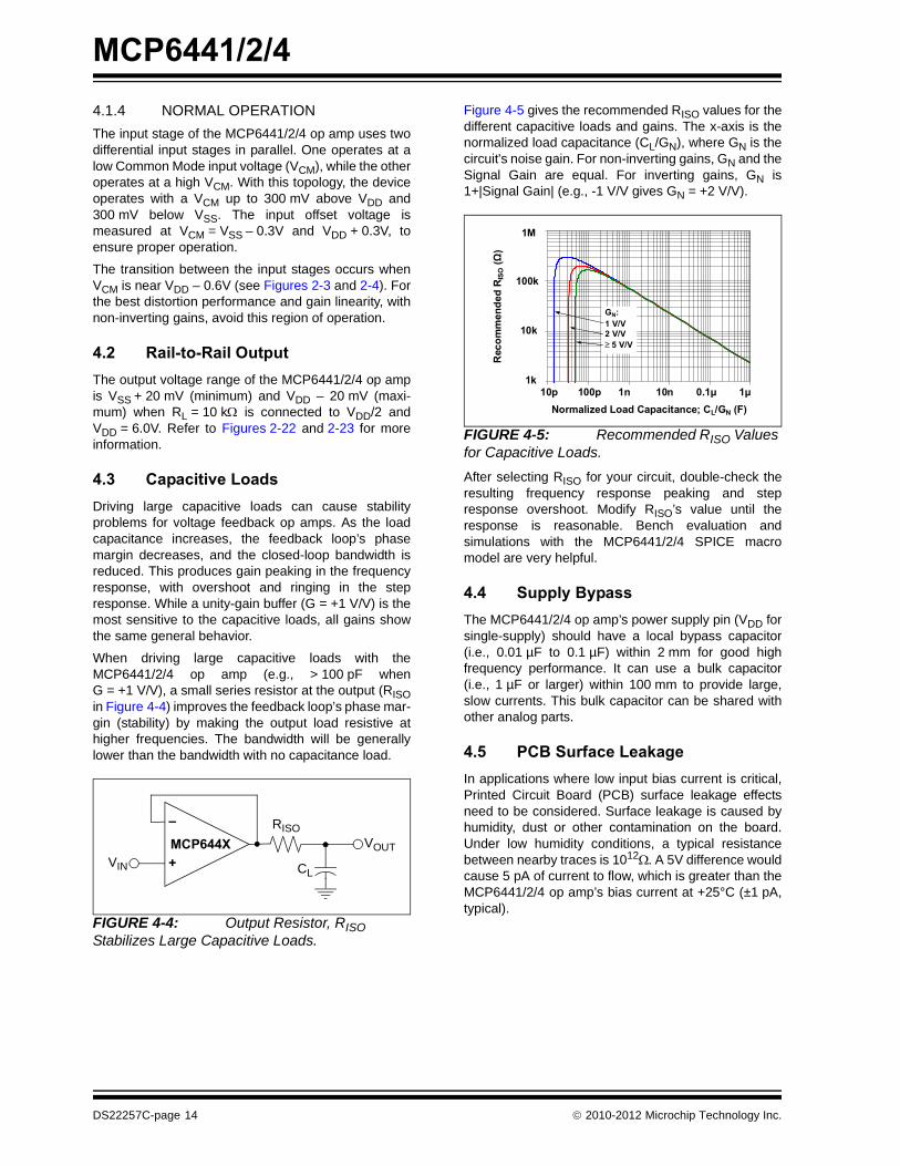
When driving large capacitive loads with theMCP6441/2/4 op amp (e.g., > 100 pF whenG = +1 V/V), a small series resistor at the output (RISOin Figure 4-4) improves the feedback loop’s phase mar-gin (stability) by making the output load resistive athigher frequencies. The bandwidth will be generallylower than the bandwidth with no capacitance load.
FIGURE 4-4: Output Resistor, RISO Stabilizes Large Capacitive Loads.
Figure 4-5 gives the recommended RISO values for thedifferent capacitive loads and gains. The x-axis is thenormalized load capacitance (CL/GN), where GN is thecircuit's noise gain. For non-inverting gains, GN and theSignal Gain are equal. For inverting gains, GN is1+|Signal Gain| (e.g., -1 V/V gives GN = +2 V/V).
FIGURE 4-5: Recommended RISO Values for Capacitive Loads.After selecting RISO for your circuit, double-check theresulting frequency response peaking and stepresponse overshoot. Modify RISO’s value until theresponse is reasonable. Bench evaluation andsimulations with the MCP6441/2/4 SPICE macromodel are very helpful.
4.4 Supply BypassThe MCP6441/2/4 op amp’s power supply pin (VDD forsingle-supply) should have a local bypass capacitor(i.e., 0.01 µF to 0.1 µF) within 2 mm for good highfrequency performance. It can use a bulk capacitor(i.e., 1 µF or larger) within 100 mm to provide large,slow currents. This bulk capacitor can be shared withother analog parts.
4.5 PCB Surface LeakageIn applications where low input bias current is critical,Printed Circuit Board (PCB) surface leakage effectsneed to be considered. Surface leakage is caused byhumidity, dust or other contamination on the board.Under low humidity conditions, a typical resistancebetween nearby traces is 1012Ω. A 5V difference wouldcause 5 pA of current to flow, which is greater than theMCP6441/2/4 op amp’s bias current at +25°C (±1 pA,typical).
VIN
RISOVOUT
CL
–
+MCP644X
1000
10000
100000
1000000
1.E-11 1.E-10 1.E-09 1.E-08 1.E-07 1.E-06Normalized Load Capacitance; CL/GN (F)
Rec
omm
ende
d R
ISO (Ω
)
GN: 1 V/V 2 V/V ≥ 5 V/V
10p 100p 1n 10n 0.1µ 1µ 1k
10k
100k
1M
DS22257C-page 14 © 2010-2012 Microchip Technology Inc.
MCP6441/2/4
The easiest way to reduce surface leakage is to use aguard ring around sensitive pins (or traces). The guardring is biased at the same voltage as the sensitive pin.An example of this type of layout is shown inFigure 4-6.FIGURE 4-6: Example Guard Ring Layout for Inverting Gain.1. Non-inverting Gain and Unity-Gain Buffer:
a) Connect the non-inverting pin (VIN+) to theinput with a wire that does not touch thePCB surface.
b) Connect the guard ring to the inverting inputpin (VIN–). This biases the guard ring to theCommon Mode input voltage.
2. Inverting Gain and Transimpedance GainAmplifiers (convert current to voltage, such asphoto detectors):a) Connect the guard ring to the non-inverting
input pin (VIN+). This biases the guard ringto the same reference voltage as the opamp (e.g., VDD/2 or ground).
b) Connect the inverting pin (VIN–) to the inputwith a wire that does not touch the PCBsurface.
4.6 Application Circuits
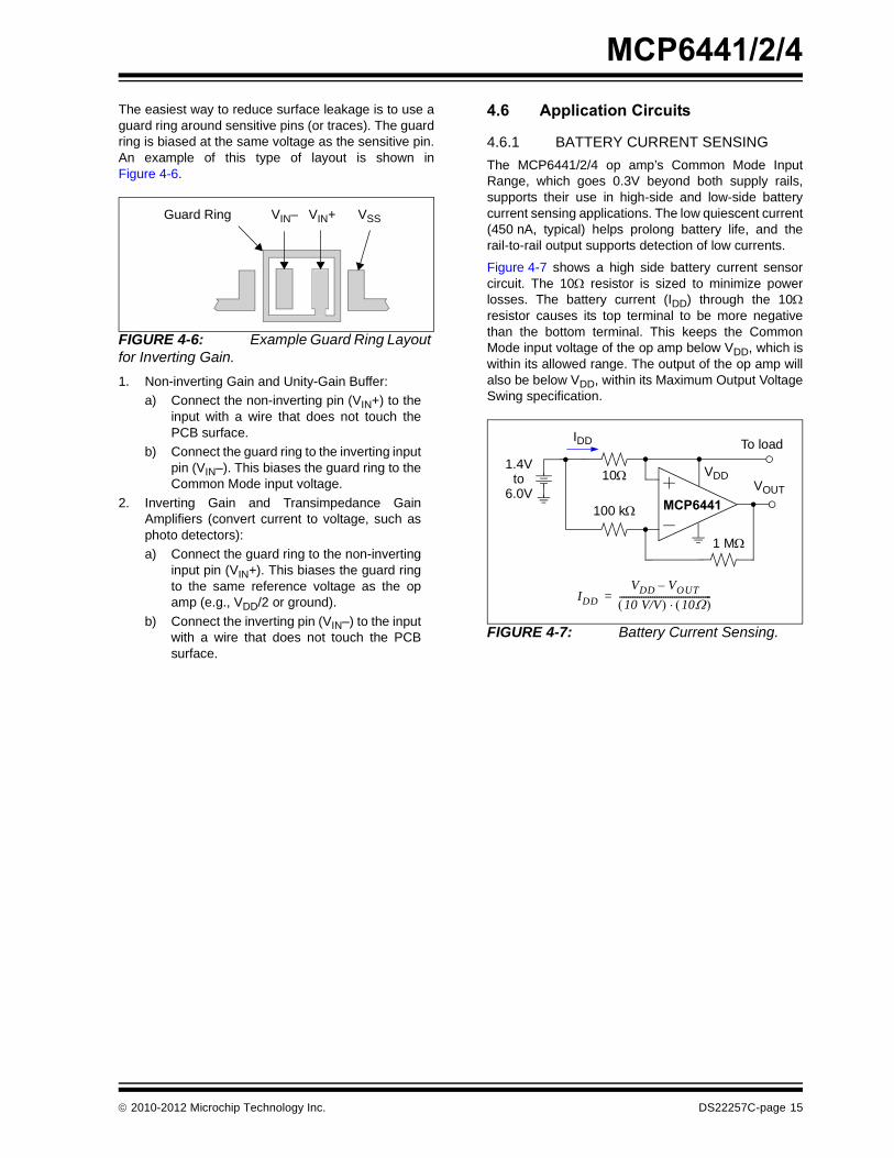
4.6.1 BATTERY CURRENT SENSINGThe MCP6441/2/4 op amp’s Common Mode InputRange, which goes 0.3V beyond both supply rails,supports their use in high-side and low-side batterycurrent sensing applications. The low quiescent current(450 nA, typical) helps prolong battery life, and therail-to-rail output supports detection of low currents.
Figure 4-7 shows a high side battery current sensorcircuit. The 10Ω resistor is sized to minimize powerlosses. The battery current (IDD) through the 10Ωresistor causes its top terminal to be more negativethan the bottom terminal. This keeps the CommonMode input voltage of the op amp below VDD, which iswithin its allowed range. The output of the op amp willalso be below VDD, within its Maximum Output VoltageSwing specification.
FIGURE 4-7: Battery Current Sensing.
Guard Ring VIN– VIN+ VSS
VDD
IDD
100 kΩ
1 MΩ
1.4VVOUT
10Ωto6.0V
IDDVDD VOUT–
10 V/V( ) 10Ω( )⋅------------------------------------------=
To load
MCP6441
© 2010-2012 Microchip Technology Inc. DS22257C-page 15
MCP6441/2/4
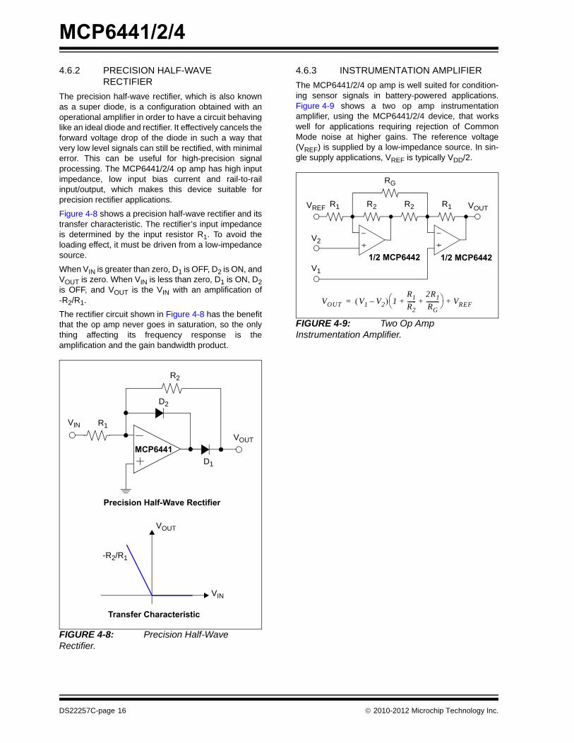
4.6.2 PRECISION HALF-WAVERECTIFIERThe precision half-wave rectifier, which is also knownas a super diode, is a configuration obtained with anoperational amplifier in order to have a circuit behavinglike an ideal diode and rectifier. It effectively cancels theforward voltage drop of the diode in such a way thatvery low level signals can still be rectified, with minimalerror. This can be useful for high-precision signalprocessing. The MCP6441/2/4 op amp has high inputimpedance, low input bias current and rail-to-railinput/output, which makes this device suitable forprecision rectifier applications.
Figure 4-8 shows a precision half-wave rectifier and itstransfer characteristic. The rectifier’s input impedanceis determined by the input resistor R1. To avoid theloading effect, it must be driven from a low-impedancesource.
When VIN is greater than zero, D1 is OFF, D2 is ON, andVOUT is zero. When VIN is less than zero, D1 is ON, D2is OFF, and VOUT is the VIN with an amplification of-R2/R1.
The rectifier circuit shown in Figure 4-8 has the benefitthat the op amp never goes in saturation, so the onlything affecting its frequency response is theamplification and the gain bandwidth product. .
FIGURE 4-8: Precision Half-Wave Rectifier.
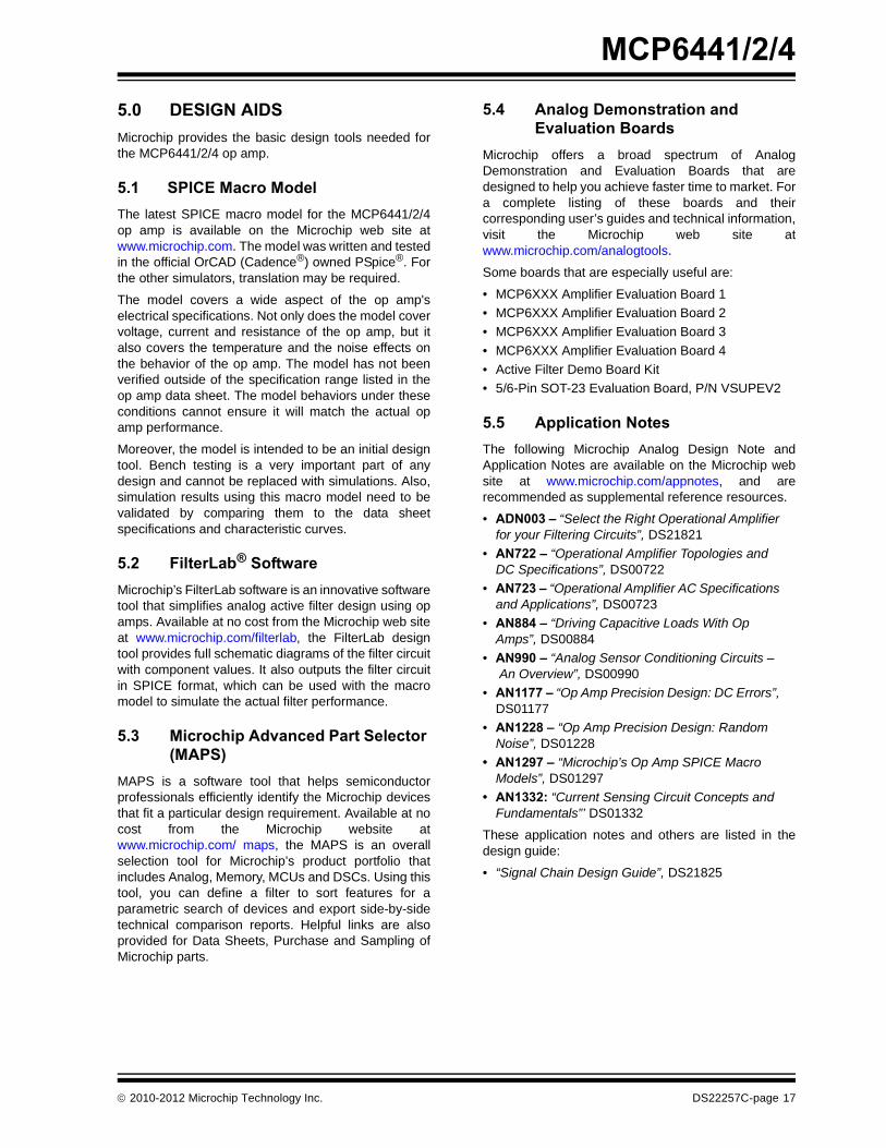
4.6.3 INSTRUMENTATION AMPLIFIERThe MCP6441/2/4 op amp is well suited for condition-ing sensor signals in battery-powered applications.Figure 4-9 shows a two op amp instrumentationamplifier, using the MCP6441/2/4 device, that workswell for applications requiring rejection of CommonMode noise at higher gains. The reference voltage(VREF) is supplied by a low-impedance source. In sin-gle supply applications, VREF is typically VDD/2.
FIGURE 4-9: Two Op Amp Instrumentation Amplifier.
VOUT
R2
D1
D2
R1VIN
VOUT
VIN
-R2/R1
Transfer Characteristic
Precision Half-Wave Rectifier
MCP6441
VOUT V1 V2–( ) 1R1R2------
2R1RG---------+ +⎝ ⎠
⎛ ⎞ VREF+=
VREF R1 R2 R2 R1 VOUT
RG
V2
V1
1/2 MCP6442 1/2 MCP6442
DS22257C-page 16 © 2010-2012 Microchip Technology Inc.
MCP6441/2/4
5.0 DESIGN AIDSMicrochip provides the basic design tools needed forthe MCP6441/2/4 op amp.
5.1 SPICE Macro ModelThe latest SPICE macro model for the MCP6441/2/4op amp is available on the Microchip web site atwww.microchip.com. The model was written and testedin the official OrCAD (Cadence®) owned PSpice®. Forthe other simulators, translation may be required.
The model covers a wide aspect of the op amp'selectrical specifications. Not only does the model covervoltage, current and resistance of the op amp, but italso covers the temperature and the noise effects onthe behavior of the op amp. The model has not beenverified outside of the specification range listed in theop amp data sheet. The model behaviors under theseconditions cannot ensure it will match the actual opamp performance.
Moreover, the model is intended to be an initial designtool. Bench testing is a very important part of anydesign and cannot be replaced with simulations. Also,simulation results using this macro model need to bevalidated by comparing them to the data sheetspecifications and characteristic curves.
5.2 FilterLab® SoftwareMicrochip’s FilterLab software is an innovative softwaretool that simplifies analog active filter design using opamps. Available at no cost from the Microchip web siteat www.microchip.com/filterlab, the FilterLab designtool provides full schematic diagrams of the filter circuitwith component values. It also outputs the filter circuitin SPICE format, which can be used with the macromodel to simulate the actual filter performance.
5.3 Microchip Advanced Part Selector (MAPS)
MAPS is a software tool that helps semiconductorprofessionals efficiently identify the Microchip devicesthat fit a particular design requirement. Available at nocost from the Microchip website atwww.microchip.com/ maps, the MAPS is an overallselection tool for Microchip’s product portfolio thatincludes Analog, Memory, MCUs and DSCs. Using thistool, you can define a filter to sort features for aparametric search of devices and export side-by-sidetechnical comparison reports. Helpful links are alsoprovided for Data Sheets, Purchase and Sampling ofMicrochip parts.
5.4 Analog Demonstration and Evaluation Boards
Microchip offers a broad spectrum of AnalogDemonstration and Evaluation Boards that aredesigned to help you achieve faster time to market. Fora complete listing of these boards and theircorresponding user’s guides and technical information,visit the Microchip web site atwww.microchip.com/analogtools.
Some boards that are especially useful are:
• MCP6XXX Amplifier Evaluation Board 1• MCP6XXX Amplifier Evaluation Board 2• MCP6XXX Amplifier Evaluation Board 3• MCP6XXX Amplifier Evaluation Board 4• Active Filter Demo Board Kit• 5/6-Pin SOT-23 Evaluation Board, P/N VSUPEV2
5.5 Application NotesThe following Microchip Analog Design Note andApplication Notes are available on the Microchip website at www.microchip.com/appnotes, and arerecommended as supplemental reference resources.
• ADN003 – “Select the Right Operational Amplifier for your Filtering Circuits”, DS21821
• AN722 – “Operational Amplifier Topologies and DC Specifications”, DS00722
• AN723 – “Operational Amplifier AC Specifications and Applications”, DS00723
• AN884 – “Driving Capacitive Loads With Op Amps”, DS00884
• AN990 – “Analog Sensor Conditioning Circuits –An Overview”, DS00990
• AN1177 – “Op Amp Precision Design: DC Errors”, DS01177
• AN1228 – “Op Amp Precision Design: Random Noise”, DS01228
• AN1297 – “Microchip’s Op Amp SPICE Macro Models”, DS01297
• AN1332: “Current Sensing Circuit Concepts and Fundamentals”’ DS01332
These application notes and others are listed in thedesign guide:
• “Signal Chain Design Guide”, DS21825
© 2010-2012 Microchip Technology Inc. DS22257C-page 17
MCP6441/2/4
NOTES:DS22257C-page 18 © 2010-2012 Microchip Technology Inc.
MCP6441/2/4
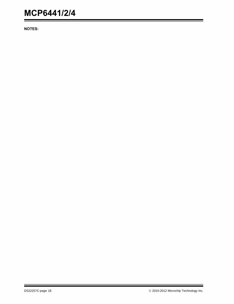
6.0 PACKAGING INFORMATION
6.1 Package Marking Information
Example:
Legend: XX...X Customer-specific informationY Year code (last digit of calendar year)YY Year code (last 2 digits of calendar year)WW Week code (week of January 1 is week ‘01’)NNN Alphanumeric traceability code Pb-free JEDEC designator for Matte Tin (Sn)* This package is Pb-free. The Pb-free JEDEC designator ( )
can be found on the outer packaging for this package.
Note: In the event the full Microchip part number cannot be marked on one line, itwill be carried over to the next line, thus limiting the number of availablecharacters for customer-specific information.
3e
3e
Example:5-Lead SOT-23 (MCP6441)
5-Lead SC70 (MCP6441)
Example:
DG25
XXNN WU25
8-Lead MSOP (MCP6442)
6442E211256
© 2010-2012 Microchip Technology Inc. DS22257C-page 19
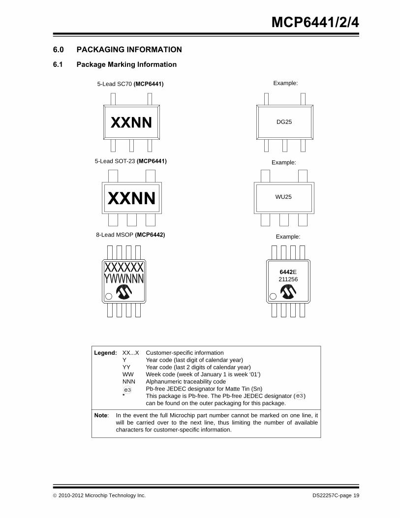
MCP6441/2/4
Legend: XX...X Customer-specific informationY Year code (last digit of calendar year)YY Year code (last 2 digits of calendar year)WW Week code (week of January 1 is week ‘01’)NNN Alphanumeric traceability code Pb-free JEDEC designator for Matte Tin (Sn)* This package is Pb-free. The Pb-free JEDEC designator ( )
can be found on the outer packaging for this package.
Note: In the event the full Microchip part number cannot be marked on one line, it willbe carried over to the next line, thus limiting the number of availablecharacters for customer-specific information.
3e
3e
14-Lead TSSOP (MCP6444) Example:
14-Lead SOIC (150 mil) (MCP6444) Example:
8-Lead SOIC (150 mil) (MCP6442) Example:
NNN
MCP6442ESN^^ 1211
2563e
8-Lead TDFN (2x3x0.75 mm)(MCP6442) Example:
AAX21125
MCP6444E/SL ^^
12112563e
YYWWNNN
XXXXXXXX 6444E/ST1211256
DS22257C-page 20 © 2010-2012 Microchip Technology Inc.
MCP6441/2/4
!"!#$!!% #$ !% #$ #&! ! !#"'(
)*+ ) #&#,$ --#$##
.# #$#/!- 0 #1/%##!###+22---2/
3# 44" " 4# 5 56 7
5$8%1 5 (1# 9()*6,:# ; < !!1/ / ; < #!%% < 6,=!# " ; !!1/=!# " ( ( (6,4# ; (.#4# 4 94! / ; < 94!=!# 8 ( <
D
b
123
E1
E
4 5e e
c
LA1
A A2
- *9)
© 2010-2012 Microchip Technology Inc. DS22257C-page 21
MCP6441/2/4
.# #$#/!- 0 #1/%##!###+22---2/
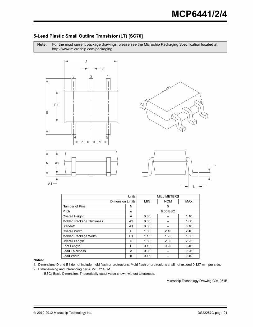
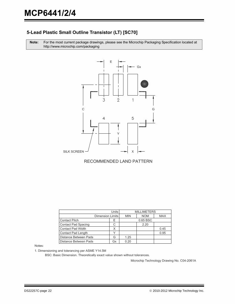
5-Lead Plastic Small Outline Transistor (LT) [SC70]
DS22257C-page 22 © 2010-2012 Microchip Technology Inc.
MCP6441/2/4
!
!"!#$!!% #$ !% #$ #&! ! !#"'(
)*+ ) #&#,$ --#$##
.# #$#/!- 0 #1/%##!###+22---2/
3# 44" " 4# 5 56 7
5$8%1 5 (4!1# ()*6$# !4!1# )*6,:# < (!!1/ / ; < #!%% < (6,=!# " < !!1/=!# " < ;6,4# < .#4# 4 < 9.## 4 ( < ;.# > < >4! / ; < 94!=!# 8 < (
φ
Nb
E
E1
D
1 2 3
e
e1
A
A1
A2 c
L
L1
- *)
© 2010-2012 Microchip Technology Inc. DS22257C-page 23
MCP6441/2/4
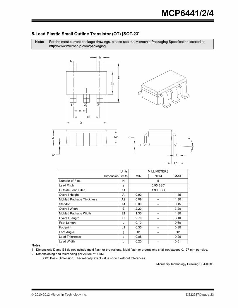
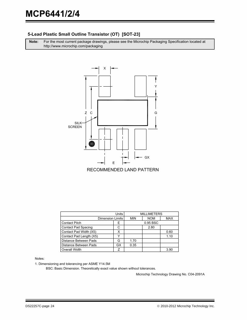
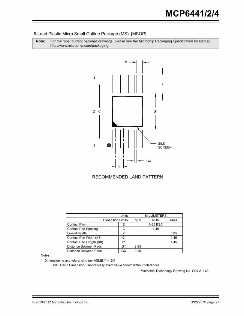
Note: For the most current package drawings, please see the Microchip Packaging Specification located at http://www.microchip.com/packaging
DS22257C-page 24 © 2010-2012 Microchip Technology Inc.
MCP6441/2/4
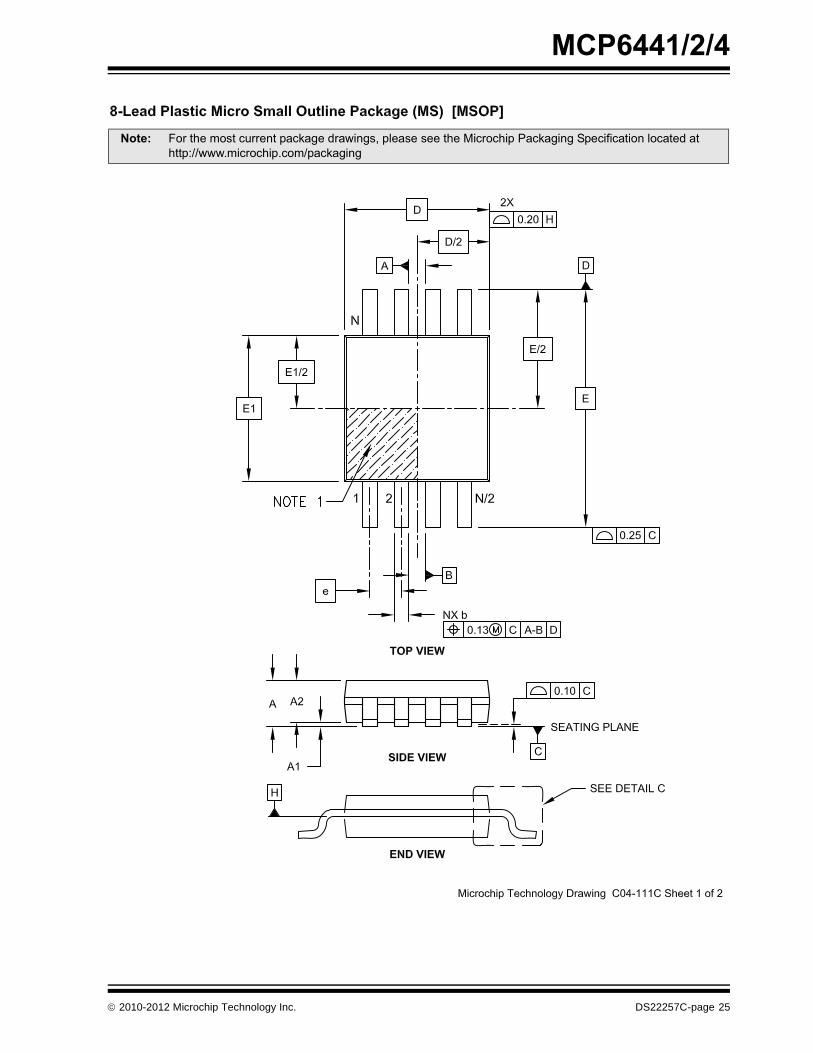
Note: For the most current package drawings, please see the Microchip Packaging Specification located at http://www.microchip.com/packaging
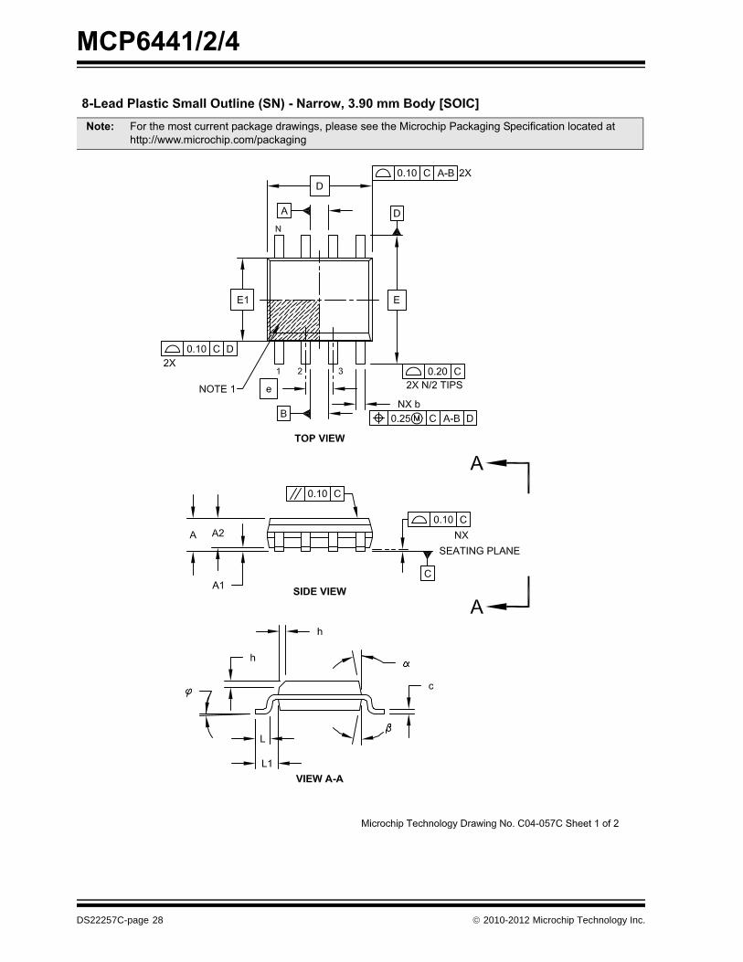
© 2010-2012 Microchip Technology Inc. DS22257C-page 25
MCP6441/2/4
Note: For the most current package drawings, please see the Microchip Packaging Specification located at http://www.microchip.com/packaging
DS22257C-page 26 © 2010-2012 Microchip Technology Inc.
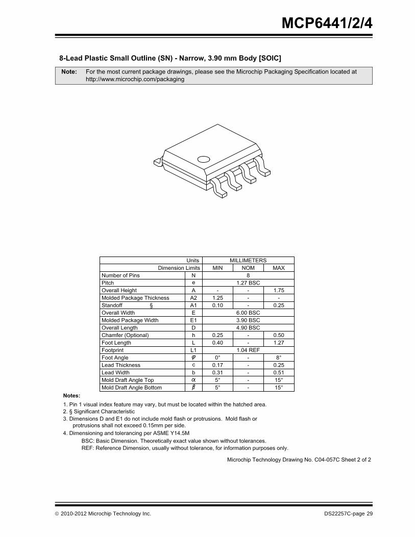
MCP6441/2/4
Note: For the most current package drawings, please see the Microchip Packaging Specification located at http://www.microchip.com/packaging
© 2010-2012 Microchip Technology Inc. DS22257C-page 27
MCP6441/2/4
Note: For the most current package drawings, please see the Microchip Packaging Specification located at http://www.microchip.com/packaging
DS22257C-page 28 © 2010-2012 Microchip Technology Inc.
MCP6441/2/4
Note: For the most current package drawings, please see the Microchip Packaging Specification located at http://www.microchip.com/packaging
© 2010-2012 Microchip Technology Inc. DS22257C-page 29
MCP6441/2/4
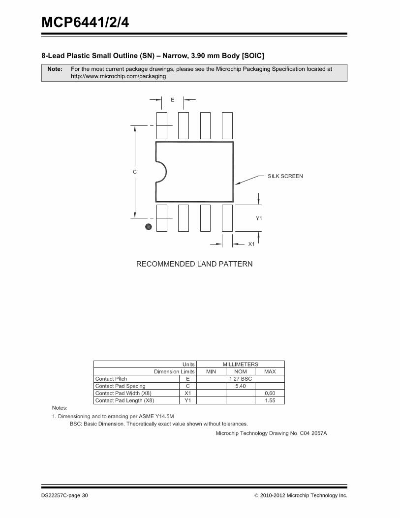
" #$%!&'()*
.# #$#/!- 0 #1/%##!###+22---2/
DS22257C-page 30 © 2010-2012 Microchip Technology Inc.
MCP6441/2/4
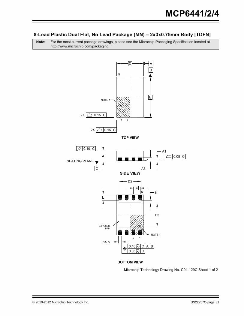
Note: For the most current package drawings, please see the Microchip Packaging Specification located at http://www.microchip.com/packaging
© 2010-2012 Microchip Technology Inc. DS22257C-page 31
MCP6441/2/4
Note: For the most current package drawings, please see the Microchip Packaging Specification located at http://www.microchip.com/packaging
DS22257C-page 32 © 2010-2012 Microchip Technology Inc.
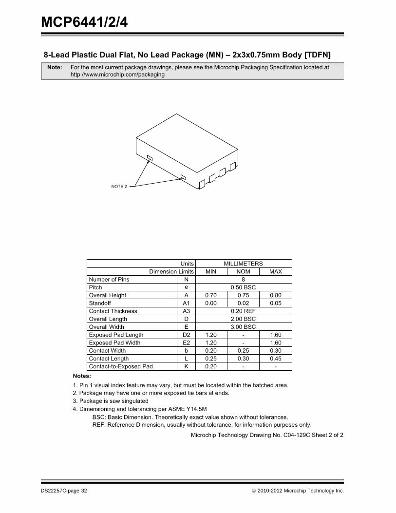
MCP6441/2/4
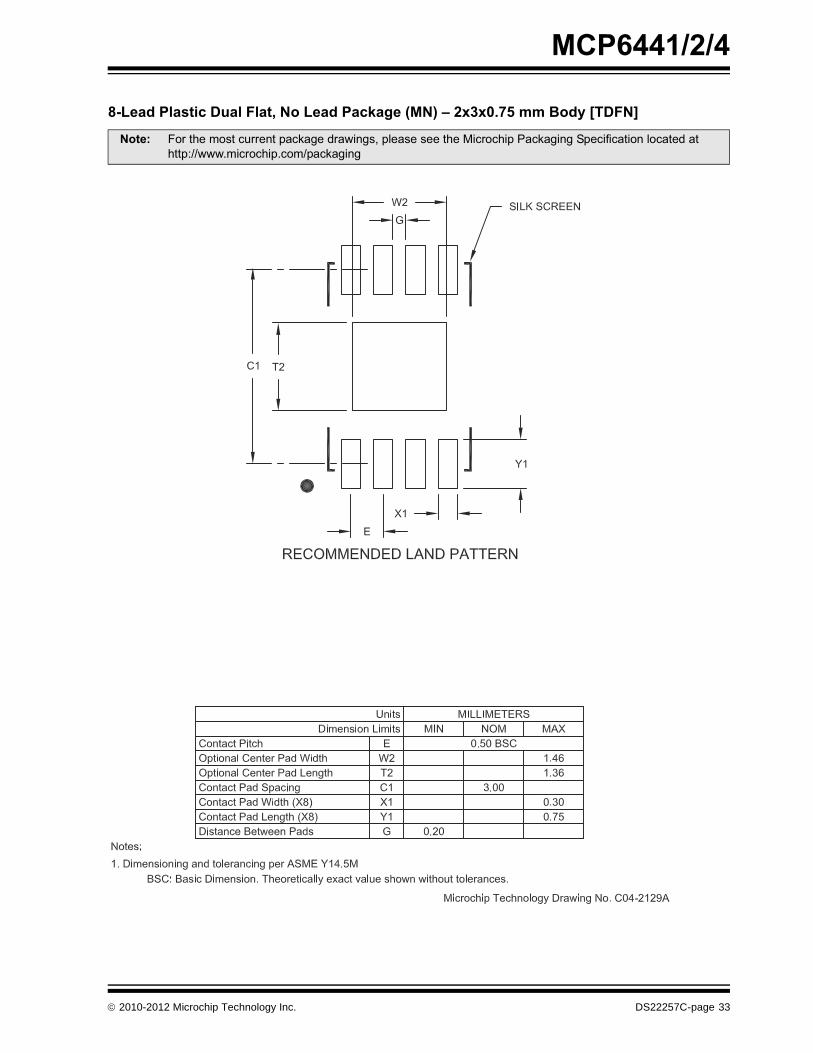
" +,%-./# 0!0&()+,
.# #$#/!- 0 #1/%##!###+22---2/
© 2010-2012 Microchip Technology Inc. DS22257C-page 33
MCP6441/2/4
Note: For the most current package drawings, please see the Microchip Packaging Specification located at http://www.microchip.com/packaging
DS22257C-page 34 © 2010-2012 Microchip Technology Inc.
MCP6441/2/4
Note: For the most current package drawings, please see the Microchip Packaging Specification located at http://www.microchip.com/packaging
© 2010-2012 Microchip Technology Inc. DS22257C-page 35
MCP6441/2/4
.# #$#/!- 0 #1/%##!###+22---2/
DS22257C-page 36 © 2010-2012 Microchip Technology Inc.
MCP6441/2/4
Note: For the most current package drawings, please see the Microchip Packaging Specification located at http://www.microchip.com/packaging
© 2010-2012 Microchip Technology Inc. DS22257C-page 37
MCP6441/2/4
Note: For the most current package drawings, please see the Microchip Packaging Specification located at http://www.microchip.com/packaging
DS22257C-page 38 © 2010-2012 Microchip Technology Inc.
MCP6441/2/4
Note: For the most current package drawings, please see the Microchip Packaging Specification located at http://www.microchip.com/packaging
© 2010-2012 Microchip Technology Inc. DS22257C-page 39

MCP6441/2/4
NOTES:DS22257C-page 40 © 2010-2012 Microchip Technology Inc.
MCP6441/2/4
APPENDIX A: REVISION HISTORY
Revision C (April 2012)The following is the list of modifications:
1. Added new package type (8-Lead 2x3 TDFN)for MCP6442, and the related informationthroughout the document.
2. Updated Table 3-1 with TDFN package pinouts.3. Updated Section 6.0, Packaging Information.4. Updated the Product Identification SysteM
section.
Revision B (March 2011)The following is the list of modifications:
1. Added the MCP6442 and MCP6444 packageinformation.
2. Updated the ESD protection value on all pins inSection 1.1, Absolute Maximum Ratings †.
3. Added Figure 2-32.4. Updated Table 3-1.5. Updated the package markings information and
drawings.6. Updated the Product Identification SysteM
section.
Revision A (September 2010)• Original Release of this Document.
© 2010-2012 Microchip Technology Inc. DS22257C-page 41

MCP6441/2/4
NOTES:DS22257C-page 42 © 2010-2012 Microchip Technology Inc.
MCP6441/2/4
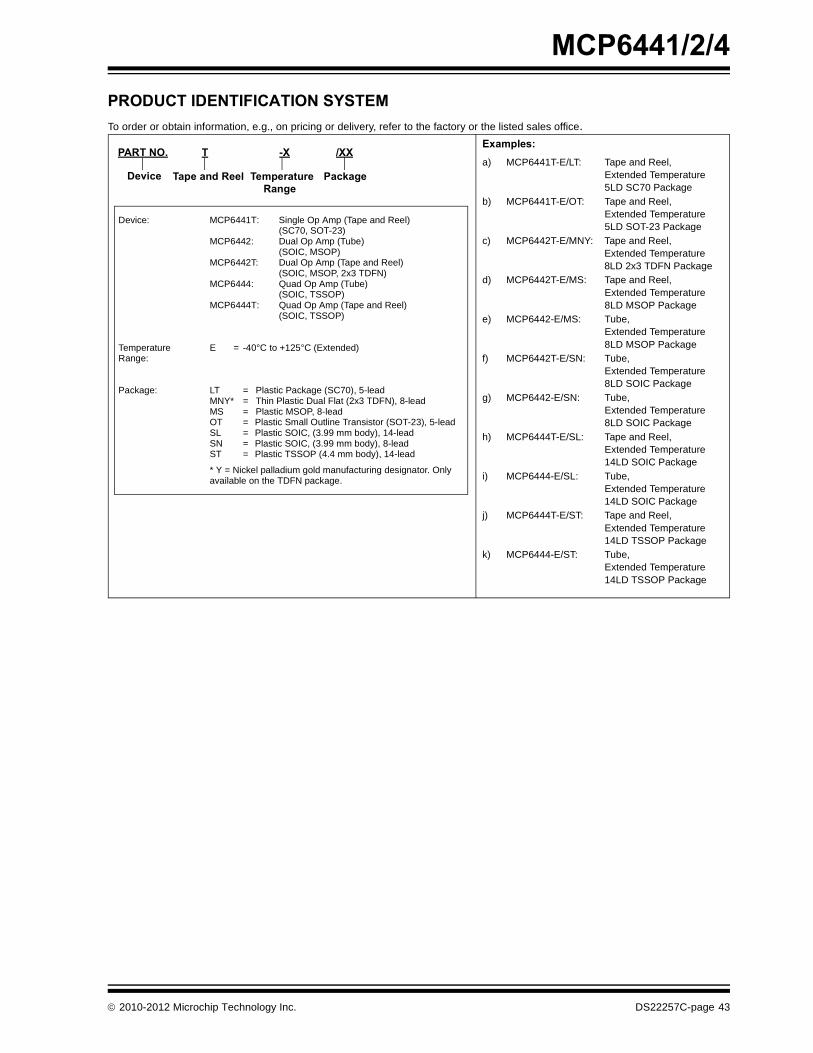
PRODUCT IDENTIFICATION SYSTEMTo order or obtain information, e.g., on pricing or delivery, refer to the factory or the listed sales office.
Device: MCP6441T: Single Op Amp (Tape and Reel)(SC70, SOT-23)
MCP6442: Dual Op Amp (Tube)(SOIC, MSOP)
MCP6442T: Dual Op Amp (Tape and Reel)(SOIC, MSOP, 2x3 TDFN)
MCP6444: Quad Op Amp (Tube)(SOIC, TSSOP)
MCP6444T: Quad Op Amp (Tape and Reel)(SOIC, TSSOP)
Temperature Range:
E = -40°C to +125°C (Extended)
Package: LT = Plastic Package (SC70), 5-leadMNY* = Thin Plastic Dual Flat (2x3 TDFN), 8-leadMS = Plastic MSOP, 8-leadOT = Plastic Small Outline Transistor (SOT-23), 5-leadSL = Plastic SOIC, (3.99 mm body), 14-leadSN = Plastic SOIC, (3.99 mm body), 8-leadST = Plastic TSSOP (4.4 mm body), 14-lead
* Y = Nickel palladium gold manufacturing designator. Only available on the TDFN package.
PART NO. -X /XX
PackageTemperatureRange
Device
T
Tape and Reel
Examples:a) MCP6441T-E/LT: Tape and Reel,
Extended Temperature5LD SC70 Package
b) MCP6441T-E/OT: Tape and Reel,Extended Temperature5LD SOT-23 Package
c) MCP6442T-E/MNY: Tape and Reel,Extended Temperature8LD 2x3 TDFN Package
d) MCP6442T-E/MS: Tape and Reel,Extended Temperature8LD MSOP Package
e) MCP6442-E/MS: Tube,Extended Temperature8LD MSOP Package
f) MCP6442T-E/SN: Tube,Extended Temperature8LD SOIC Package
g) MCP6442-E/SN: Tube,Extended Temperature8LD SOIC Package
h) MCP6444T-E/SL: Tape and Reel,Extended Temperature14LD SOIC Package
i) MCP6444-E/SL: Tube,Extended Temperature14LD SOIC Package
j) MCP6444T-E/ST: Tape and Reel,Extended Temperature14LD TSSOP Package
k) MCP6444-E/ST: Tube,Extended Temperature14LD TSSOP Package
© 2010-2012 Microchip Technology Inc. DS22257C-page 43

MCP6441/2/4
NOTES:DS22257C-page 44 © 2010-2012 Microchip Technology Inc.
Note the following details of the code protection feature on Microchip devices:• Microchip products meet the specification contained in their particular Microchip Data Sheet.
• Microchip believes that its family of products is one of the most secure families of its kind on the market today, when used in the intended manner and under normal conditions.
• There are dishonest and possibly illegal methods used to breach the code protection feature. All of these methods, to our knowledge, require using the Microchip products in a manner outside the operating specifications contained in Microchip’s Data Sheets. Most likely, the person doing so is engaged in theft of intellectual property.
• Microchip is willing to work with the customer who is concerned about the integrity of their code.
• Neither Microchip nor any other semiconductor manufacturer can guarantee the security of their code. Code protection does not mean that we are guaranteeing the product as “unbreakable.”
Code protection is constantly evolving. We at Microchip are committed to continuously improving the code protection features of ourproducts. Attempts to break Microchip’s code protection feature may be a violation of the Digital Millennium Copyright Act. If such actsallow unauthorized access to your software or other copyrighted work, you may have a right to sue for relief under that Act.
Information contained in this publication regarding deviceapplications and the like is provided only for your convenienceand may be superseded by updates. It is your responsibility toensure that your application meets with your specifications.MICROCHIP MAKES NO REPRESENTATIONS ORWARRANTIES OF ANY KIND WHETHER EXPRESS ORIMPLIED, WRITTEN OR ORAL, STATUTORY OROTHERWISE, RELATED TO THE INFORMATION,INCLUDING BUT NOT LIMITED TO ITS CONDITION,QUALITY, PERFORMANCE, MERCHANTABILITY ORFITNESS FOR PURPOSE. Microchip disclaims all liabilityarising from this information and its use. Use of Microchipdevices in life support and/or safety applications is entirely atthe buyer’s risk, and the buyer agrees to defend, indemnify andhold harmless Microchip from any and all damages, claims,suits, or expenses resulting from such use. No licenses areconveyed, implicitly or otherwise, under any Microchipintellectual property rights.
© 2010-2012 Microchip Technology Inc.
QUALITY MANAGEMENT SYSTEM CERTIFIED BY DNV
== ISO/TS 16949 ==
Trademarks
The Microchip name and logo, the Microchip logo, dsPIC, KEELOQ, KEELOQ logo, MPLAB, PIC, PICmicro, PICSTART, PIC32 logo, rfPIC and UNI/O are registered trademarks of Microchip Technology Incorporated in the U.S.A. and other countries.
FilterLab, Hampshire, HI-TECH C, Linear Active Thermistor, MXDEV, MXLAB, SEEVAL and The Embedded Control Solutions Company are registered trademarks of Microchip Technology Incorporated in the U.S.A.
Analog-for-the-Digital Age, Application Maestro, chipKIT, chipKIT logo, CodeGuard, dsPICDEM, dsPICDEM.net, dsPICworks, dsSPEAK, ECAN, ECONOMONITOR, FanSense, HI-TIDE, In-Circuit Serial Programming, ICSP, Mindi, MiWi, MPASM, MPLAB Certified logo, MPLIB, MPLINK, mTouch, Omniscient Code Generation, PICC, PICC-18, PICDEM, PICDEM.net, PICkit, PICtail, REAL ICE, rfLAB, Select Mode, Total Endurance, TSHARC, UniWinDriver, WiperLock and ZENA are trademarks of Microchip Technology Incorporated in the U.S.A. and other countries.
SQTP is a service mark of Microchip Technology Incorporated in the U.S.A.
All other trademarks mentioned herein are property of their respective companies.
© 2010-2012, Microchip Technology Incorporated, Printed in the U.S.A., All Rights Reserved.
Printed on recycled paper.
ISBN: 978-1-62076-244-8
DS22257C-page 45
Microchip received ISO/TS-16949:2009 certification for its worldwide headquarters, design and wafer fabrication facilities in Chandler and Tempe, Arizona; Gresham, Oregon and design centers in California and India. The Company’s quality system processes and procedures are for its PIC® MCUs and dsPIC® DSCs, KEELOQ® code hopping devices, Serial EEPROMs, microperipherals, nonvolatile memory and analog products. In addition, Microchip’s quality system for the design and manufacture of development systems is ISO 9001:2000 certified.
DS22257C-page 46 © 2010-2012 Microchip Technology Inc.
AMERICASCorporate Office2355 West Chandler Blvd.Chandler, AZ 85224-6199Tel: 480-792-7200 Fax: 480-792-7277Technical Support: http://www.microchip.com/supportWeb Address: www.microchip.comAtlantaDuluth, GA Tel: 678-957-9614 Fax: 678-957-1455BostonWestborough, MA Tel: 774-760-0087 Fax: 774-760-0088ChicagoItasca, IL Tel: 630-285-0071 Fax: 630-285-0075ClevelandIndependence, OH Tel: 216-447-0464 Fax: 216-447-0643DallasAddison, TX Tel: 972-818-7423 Fax: 972-818-2924DetroitFarmington Hills, MI Tel: 248-538-2250Fax: 248-538-2260IndianapolisNoblesville, IN Tel: 317-773-8323Fax: 317-773-5453Los AngelesMission Viejo, CA Tel: 949-462-9523 Fax: 949-462-9608Santa ClaraSanta Clara, CA Tel: 408-961-6444Fax: 408-961-6445TorontoMississauga, Ontario, CanadaTel: 905-673-0699 Fax: 905-673-6509
ASIA/PACIFICAsia Pacific OfficeSuites 3707-14, 37th FloorTower 6, The GatewayHarbour City, KowloonHong KongTel: 852-2401-1200Fax: 852-2401-3431Australia - SydneyTel: 61-2-9868-6733Fax: 61-2-9868-6755China - BeijingTel: 86-10-8569-7000 Fax: 86-10-8528-2104China - ChengduTel: 86-28-8665-5511Fax: 86-28-8665-7889China - ChongqingTel: 86-23-8980-9588Fax: 86-23-8980-9500China - HangzhouTel: 86-571-2819-3187 Fax: 86-571-2819-3189China - Hong Kong SARTel: 852-2401-1200 Fax: 852-2401-3431China - NanjingTel: 86-25-8473-2460Fax: 86-25-8473-2470China - QingdaoTel: 86-532-8502-7355Fax: 86-532-8502-7205China - ShanghaiTel: 86-21-5407-5533 Fax: 86-21-5407-5066China - ShenyangTel: 86-24-2334-2829Fax: 86-24-2334-2393China - ShenzhenTel: 86-755-8203-2660 Fax: 86-755-8203-1760China - WuhanTel: 86-27-5980-5300Fax: 86-27-5980-5118China - XianTel: 86-29-8833-7252Fax: 86-29-8833-7256China - XiamenTel: 86-592-2388138 Fax: 86-592-2388130China - ZhuhaiTel: 86-756-3210040 Fax: 86-756-3210049
ASIA/PACIFICIndia - BangaloreTel: 91-80-3090-4444 Fax: 91-80-3090-4123India - New DelhiTel: 91-11-4160-8631Fax: 91-11-4160-8632India - PuneTel: 91-20-2566-1512Fax: 91-20-2566-1513Japan - OsakaTel: 81-66-152-7160 Fax: 81-66-152-9310Japan - YokohamaTel: 81-45-471- 6166 Fax: 81-45-471-6122Korea - DaeguTel: 82-53-744-4301Fax: 82-53-744-4302Korea - SeoulTel: 82-2-554-7200Fax: 82-2-558-5932 or 82-2-558-5934Malaysia - Kuala LumpurTel: 60-3-6201-9857Fax: 60-3-6201-9859Malaysia - PenangTel: 60-4-227-8870Fax: 60-4-227-4068Philippines - ManilaTel: 63-2-634-9065Fax: 63-2-634-9069SingaporeTel: 65-6334-8870Fax: 65-6334-8850Taiwan - Hsin ChuTel: 886-3-5778-366Fax: 886-3-5770-955Taiwan - KaohsiungTel: 886-7-536-4818Fax: 886-7-330-9305Taiwan - TaipeiTel: 886-2-2500-6610 Fax: 886-2-2508-0102Thailand - BangkokTel: 66-2-694-1351Fax: 66-2-694-1350
EUROPEAustria - WelsTel: 43-7242-2244-39Fax: 43-7242-2244-393Denmark - CopenhagenTel: 45-4450-2828 Fax: 45-4485-2829France - ParisTel: 33-1-69-53-63-20 Fax: 33-1-69-30-90-79Germany - MunichTel: 49-89-627-144-0 Fax: 49-89-627-144-44Italy - Milan Tel: 39-0331-742611 Fax: 39-0331-466781Netherlands - DrunenTel: 31-416-690399 Fax: 31-416-690340Spain - MadridTel: 34-91-708-08-90Fax: 34-91-708-08-91UK - WokinghamTel: 44-118-921-5869Fax: 44-118-921-5820
Worldwide Sales and Service
11/29/11