50 mhz to 2 ghz quadrature demodulator adl5387phil/hardware/usrp/adl5387_datasheet.pdf50 mhz to 2...
TRANSCRIPT
50 MHz to 2 GHzQuadrature Demodulator
ADL5387
Rev. 0 Information furnished by Analog Devices is believed to be accurate and reliable. However, no responsibility is assumed by Analog Devices for its use, nor for any infringements of patents or other rights of third parties that may result from its use. Specifications subject to change without notice. No license is granted by implication or otherwise under any patent or patent rights of Analog Devices. Trademarks and registered trademarks are the property of their respective owners.
One Technology Way, P.O. Box 9106, Norwood, MA 02062-9106, U.S.A.Tel: 781.329.4700 www.analog.com Fax: 781.461.3113 ©2007 Analog Devices, Inc. All rights reserved.
FEATURES Operating RF frequency
50 MHz to 2 GHz LO input at 2 × fLO
100 MHz to 4 GHz Input IP3: 31 dBm @ 900 MHz Input IP2: 62 dBm @ 900 MHz Input P1dB: 13 dBm @ 900 MHz Noise figure (NF)
12.0 dB @ 140 MHz 14.7 dB @ 900 MHz
Voltage conversion gain > 4 dB Quadrature demodulation accuracy
Phase accuracy ~0.4° Amplitude balance ~0.05 dB
Demodulation bandwidth ~240 MHz Baseband I/Q drive 2 V p-p into 200 Ω Single 5 V supply
APPLICATIONS QAM/QPSK RF/IF demodulators W-CDMA/CDMA/CDMA2000/GSM Microwave point-to-(multi)point radios Broadband wireless and WiMAX Broadband CATVs
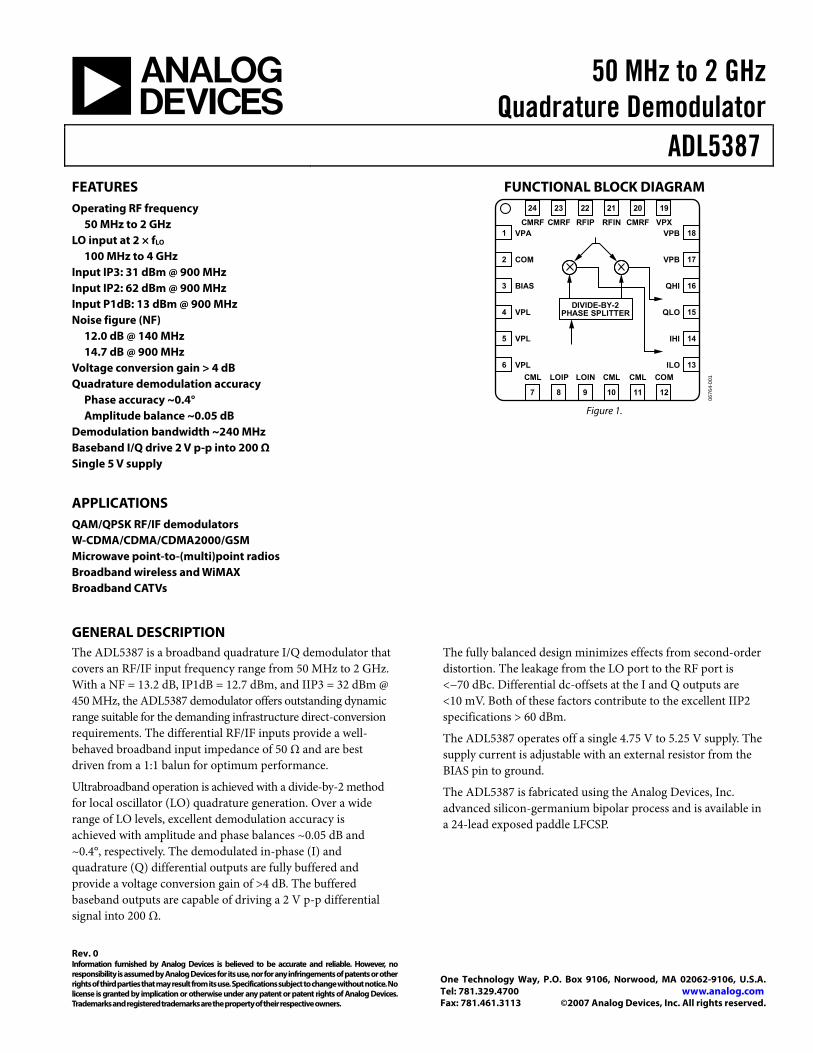
FUNCTIONAL BLOCK DIAGRAM
DIVIDE-BY-2PHASE SPLITTER
1
24
CMRF CMRF RFIP RFIN CMRF VPX
CML
VPA
COM
BIAS
VPL
VPL
VPL
VPB
VPB
QHI
QLO
IHI
ILOLOIP LOIN CML CML COM
23 22 21 20 19
7 8 9 10 11 12
2
3
4
5
6
18
17
16
15
14
13
0676
4-00
1
Figure 1.
GENERAL DESCRIPTION The ADL5387 is a broadband quadrature I/Q demodulator that covers an RF/IF input frequency range from 50 MHz to 2 GHz. With a NF = 13.2 dB, IP1dB = 12.7 dBm, and IIP3 = 32 dBm @ 450 MHz, the ADL5387 demodulator offers outstanding dynamic range suitable for the demanding infrastructure direct-conversion requirements. The differential RF/IF inputs provide a well-behaved broadband input impedance of 50 Ω and are best driven from a 1:1 balun for optimum performance.
Ultrabroadband operation is achieved with a divide-by-2 method for local oscillator (LO) quadrature generation. Over a wide range of LO levels, excellent demodulation accuracy is achieved with amplitude and phase balances ~0.05 dB and ~0.4°, respectively. The demodulated in-phase (I) and quadrature (Q) differential outputs are fully buffered and provide a voltage conversion gain of >4 dB. The buffered baseband outputs are capable of driving a 2 V p-p differential signal into 200 Ω.
The fully balanced design minimizes effects from second-order distortion. The leakage from the LO port to the RF port is <−70 dBc. Differential dc-offsets at the I and Q outputs are <10 mV. Both of these factors contribute to the excellent IIP2 specifications > 60 dBm.
The ADL5387 operates off a single 4.75 V to 5.25 V supply. The supply current is adjustable with an external resistor from the BIAS pin to ground.
The ADL5387 is fabricated using the Analog Devices, Inc. advanced silicon-germanium bipolar process and is available in a 24-lead exposed paddle LFCSP.
ADL5387
Rev. 0 | Page 2 of 28
TABLE OF CONTENTS Features .............................................................................................. 1 Applications....................................................................................... 1 Functional Block Diagram .............................................................. 1 General Description ......................................................................... 1 Revision History ............................................................................... 2 Specifications..................................................................................... 3 Absolute Maximum Ratings............................................................ 5
ESD Caution.................................................................................. 5 Pin Configuration and Function Descriptions............................. 6 Typical Performance Characteristics ............................................. 7
Distributions for fRF = 140 MHz ............................................... 10 Distributions for fRF = 450 MHz ............................................... 11 Distributions for fRF = 900 MHz ............................................... 12 Distributions for fRF = 1900 MHz............................................. 13
Circuit Description......................................................................... 14 LO Interface................................................................................. 14 V-to-I Converter......................................................................... 14
Mixers .......................................................................................... 14 Emitter Follower Buffers ........................................................... 14 Bias Circuit .................................................................................. 14
Applications..................................................................................... 15 Basic Connections...................................................................... 15 Power Supply............................................................................... 15 Local Oscillator (LO) Input ...................................................... 15 RF Input....................................................................................... 16 Baseband Outputs ...................................................................... 16 Error Vector Magnitude (EVM) Performance ....................... 17 Low IF Image Rejection............................................................. 18 Example Baseband Interface..................................................... 18
Characterization Setups................................................................. 21 Evaluation Board ............................................................................ 23 Outline Dimensions ....................................................................... 26
Ordering Guide .......................................................................... 26
REVISION HISTORY 10/07—Revision 0: Initial Version
ADL5387
Rev. 0 | Page 3 of 28
SPECIFICATIONS VS = 5 V, TA = 25°C, fRF = 900 MHz, fIF = 4.5 MHz, PLO = 0 dBm, BIAS pin open, ZO = 50 Ω, unless otherwise noted, baseband outputs differentially loaded with 450 Ω.
Table 1. Parameter Condition Min Typ Max Unit OPERATING CONDITIONS
LO Frequency Range External input = 2xLO frequency 0.1 4 GHz RF Frequency Range 0.05 2 GHz
LO INPUT LOIP, LOIN
Input Return Loss AC-coupled into LOIP with LOIN bypassed, measured at 2 GHz
−10 dB
LO Input Level −6 0 +6 dBm I/Q BASEBAND OUTPUTS QHI, QLO, IHI, ILO
Voltage Conversion Gain 450 Ω differential load on I and Q outputs (@ 900 MHz)
4.3 dB
200 Ω differential load on I and Q outputs (@ 900 MHz)
3.2 dB
Demodulation Bandwidth 1 V p-p signal 3 dB bandwidth 240 MHz Quadrature Phase Error @ 900 MHz 0.4 Degrees I/Q Amplitude Imbalance 0.1 dB Output DC Offset (Differential) 0 dBm LO input ±5 mV Output Common-Mode VPOS − 2.8 V 0.1 dB Gain Flatness 40 MHz Output Swing Differential 200 Ω load 2 V p-p Peak Output Current Each pin 12 mA
POWER SUPPLIES VPA, VPL, VPB, VPX Voltage 4.75 5.25 V Current BIAS pin open 180 mA
RBIAS = 4 kΩ 157 mA DYNAMIC PERFORMANCE @ RF = 140 MHz RFIP, RFIN
Conversion Gain 4.7 dB Input P1dB (IP1dB) 13 dBm Second-Order Input Intercept (IIP2) −5 dBm each input tone 67 dBm Third-Order Input Intercept (IIP3) −5 dBm each input tone 31 dBm LO to RF RFIN, RFIP terminated in 50 Ω, 1xLO
appearing at the RF port −100 dBm
RF to LO LOIN, LOIP terminated in 50 Ω −95 dBc I/Q Magnitude Imbalance 0.05 dB I/Q Phase Imbalance 0.2 Degrees LO to I/Q RFIN, RFIP terminated in 50 Ω, 1xLO
appearing at the BB port −39 dBm
Noise Figure 12.0 dB Noise Figure under Blocking Conditions With a −5 dBm interferer 5 MHz away 14.4 dB
ADL5387
Rev. 0 | Page 4 of 28
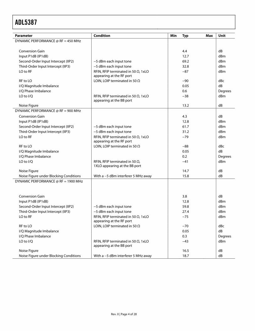
Parameter Condition Min Typ Max Unit DYNAMIC PERFORMANCE @ RF = 450 MHz
Conversion Gain 4.4 dB Input P1dB (IP1dB) 12.7 dBm Second-Order Input Intercept (IIP2) −5 dBm each input tone 69.2 dBm Third-Order Input Intercept (IIP3) −5 dBm each input tone 32.8 dBm LO to RF RFIN, RFIP terminated in 50 Ω, 1xLO
appearing at the RF port −87 dBm
RF to LO LOIN, LOIP terminated in 50 Ω −90 dBc I/Q Magnitude Imbalance 0.05 dB I/Q Phase Imbalance 0.6 Degrees LO to I/Q RFIN, RFIP terminated in 50 Ω, 1xLO
appearing at the BB port −38 dBm
Noise Figure 13.2 dB DYNAMIC PERFORMANCE @ RF = 900 MHz
Conversion Gain 4.3 dB Input P1dB (IP1dB) 12.8 dBm Second-Order Input Intercept (IIP2) −5 dBm each input tone 61.7 dBm Third-Order Input Intercept (IIP3) −5 dBm each input tone 31.2 dBm LO to RF RFIN, RFIP terminated in 50 Ω, 1xLO
appearing at the RF port −79 dBm
RF to LO LOIN, LOIP terminated in 50 Ω −88 dBc I/Q Magnitude Imbalance 0.05 dB I/Q Phase Imbalance 0.2 Degrees LO to I/Q RFIN, RFIP terminated in 50 Ω,
1XLO appearing at the BB port −41 dBm
Noise Figure 14.7 dB Noise Figure under Blocking Conditions With a −5 dBm interferer 5 MHz away 15.8 dB
DYNAMIC PERFORMANCE @ RF = 1900 MHz
Conversion Gain 3.8 dB Input P1dB (IP1dB) 12.8 dBm Second-Order Input Intercept (IIP2) −5 dBm each input tone 59.8 dBm Third-Order Input Intercept (IIP3) −5 dBm each input tone 27.4 dBm LO to RF RFIN, RFIP terminated in 50 Ω, 1xLO
appearing at the RF port −75 dBm
RF to LO LOIN, LOIP terminated in 50 Ω −70 dBc I/Q Magnitude Imbalance 0.05 dB I/Q Phase Imbalance 0.3 Degrees LO to I/Q RFIN, RFIP terminated in 50 Ω, 1xLO
appearing at the BB port −43 dBm
Noise Figure 16.5 dB Noise Figure under Blocking Conditions With a −5 dBm interferer 5 MHz away 18.7 dB
ADL5387
Rev. 0 | Page 5 of 28
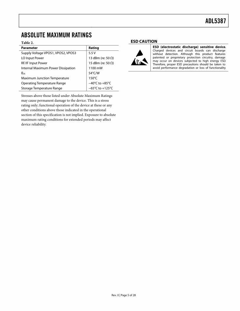
ABSOLUTE MAXIMUM RATINGS Table 2. Parameter Rating
Supply Voltage VPOS1, VPOS2, VPOS3 5.5 V
LO Input Power 13 dBm (re: 50 Ω)
RF/IF Input Power 15 dBm (re: 50 Ω)
Internal Maximum Power Dissipation 1100 mW
θJA 54°C/W
Maximum Junction Temperature 150°C
Operating Temperature Range −40°C to +85°C
Storage Temperature Range −65°C to +125°C
Stresses above those listed under Absolute Maximum Ratings may cause permanent damage to the device. This is a stress rating only; functional operation of the device at these or any other conditions above those indicated in the operational section of this specification is not implied. Exposure to absolute maximum rating conditions for extended periods may affect device reliability.
ESD CAUTION
ADL5387
Rev. 0 | Page 6 of 28
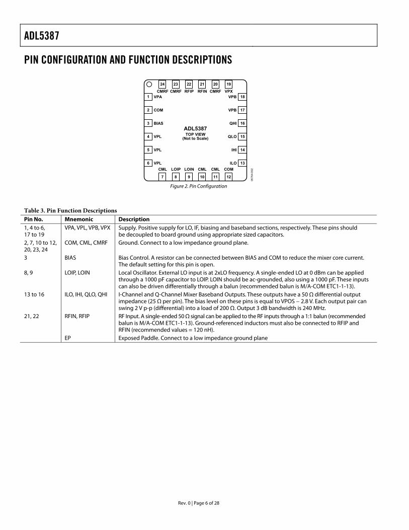
PIN CONFIGURATION AND FUNCTION DESCRIPTIONS
1
24
CMRF CMRF RFIP
ADL5387TOP VIEW
(Not to Scale)
RFIN CMRF VPX
CML
VPA
COM
BIAS
VPL
VPL
VPL
VPB
VPB
QHI
QLO
IHI
ILOLOIP LOIN CML CML COM
23 22 21 20 19
7 8 9 10 11 12
2
3
4
5
6
18
17
16
15
14
13
0676
4-00
2
Figure 2. Pin Configuration
Table 3. Pin Function Descriptions Pin No. Mnemonic Description 1, 4 to 6, 17 to 19
VPA, VPL, VPB, VPX Supply. Positive supply for LO, IF, biasing and baseband sections, respectively. These pins should be decoupled to board ground using appropriate sized capacitors.
2, 7, 10 to 12, 20, 23, 24
COM, CML, CMRF Ground. Connect to a low impedance ground plane.
3 BIAS Bias Control. A resistor can be connected between BIAS and COM to reduce the mixer core current. The default setting for this pin is open.
8, 9 LOIP, LOIN Local Oscillator. External LO input is at 2xLO frequency. A single-ended LO at 0 dBm can be applied through a 1000 pF capacitor to LOIP. LOIN should be ac-grounded, also using a 1000 pF. These inputs can also be driven differentially through a balun (recommended balun is M/A-COM ETC1-1-13).
13 to 16 ILO, IHI, QLO, QHI I-Channel and Q-Channel Mixer Baseband Outputs. These outputs have a 50 Ω differential output impedance (25 Ω per pin). The bias level on these pins is equal to VPOS − 2.8 V. Each output pair can swing 2 V p-p (differential) into a load of 200 Ω. Output 3 dB bandwidth is 240 MHz.
21, 22 RFIN, RFIP RF Input. A single-ended 50 Ω signal can be applied to the RF inputs through a 1:1 balun (recommended balun is M/A-COM ETC1-1-13). Ground-referenced inductors must also be connected to RFIP and RFIN (recommended values = 120 nH).
EP Exposed Paddle. Connect to a low impedance ground plane
ADL5387
Rev. 0 | Page 7 of 28
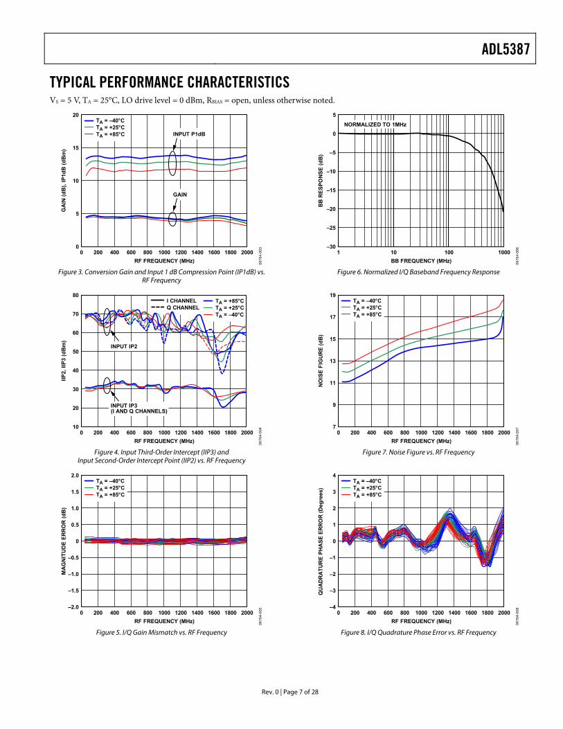
TYPICAL PERFORMANCE CHARACTERISTICS VS = 5 V, TA = 25°C, LO drive level = 0 dBm, RBIAS = open, unless otherwise noted.
20
15
10
5
00 200 400 600 800 1000 1200 1400 1600 1800 2000
GA
IN (d
B),
IP1d
B (d
Bm
)
RF FREQUENCY (MHz)
GAIN
INPUT P1dBTA = +85°CTA = +25°CTA = –40°C
0676
4-00
3
Figure 3. Conversion Gain and Input 1 dB Compression Point (IP1dB) vs. RF Frequency
80
70
50
30
60
40
20
100 200 400 600 800 1000 1200 1400 1600 1800 2000
IIP2,
IIP3
(dB
m)
RF FREQUENCY (MHz)
TA = –40°CTA = +25°CTA = +85°C
Q CHANNELI CHANNEL
INPUT IP3(I AND Q CHANNELS)
INPUT IP2
0676
4-00
4
Figure 4. Input Third-Order Intercept (IIP3) and
Input Second-Order Intercept Point (IIP2) vs. RF Frequency
2.0
1.5
1.0
0.5
0
–0.5
–1.0
–1.5
–2.00 200 400 600 800 1000 1200 1400 1600 1800 2000
MA
GN
ITU
DE
ERR
OR
(dB
)
RF FREQUENCY (MHz)
TA = +85°CTA = +25°CTA = –40°C
0676
4-00
5
Figure 5. I/Q Gain Mismatch vs. RF Frequency
5
–30
–25
–20
–15
–10
–5
0
1 100010010
BB
RES
PON
SE (d
B)
BB FREQUENCY (MHz) 0676
4-00
6
NORMALIZED TO 1MHz
Figure 6. Normalized I/Q Baseband Frequency Response
19
17
15
13
11
9
70 200 400 600 800 1000 1200 1400 1600 1800 2000
NO
ISE
FIG
UR
E (d
B)
RF FREQUENCY (MHz)
TA = +85°CTA = +25°CTA = –40°C
0676
4-00
7
Figure 7. Noise Figure vs. RF Frequency
4
3
2
1
0
–1
–2
–3
–40 200 400 600 800 1000 1200 1400 1600 1800 2000
QU
AD
RA
TUR
E PH
ASE
ER
RO
R (D
egre
es)
RF FREQUENCY (MHz)
TA = +85°CTA = +25°CTA = –40°C
0676
4-00
8
Figure 8. I/Q Quadrature Phase Error vs. RF Frequency
ADL5387
Rev. 0 | Page 8 of 28
20
15
10
5
0–6 –5 –4 –3 –2 –1 0 1 2 3 4 5 6
GA
IN (d
B),
INPU
T P1
dB (d
Bm
), N
OIS
E FI
GU
RE
(dB
) 80
65
50
35
20
INPU
T IP
2, IN
PUT
IP3
(dB
m)
LO LEVEL (dBm)
INPUT IP2, Q CHANNEL
INPUT P1dB
GAIN
INPUT IP3
NOISE FIGURE
INPUT IP2, I CHANNEL
0676
4-00
9
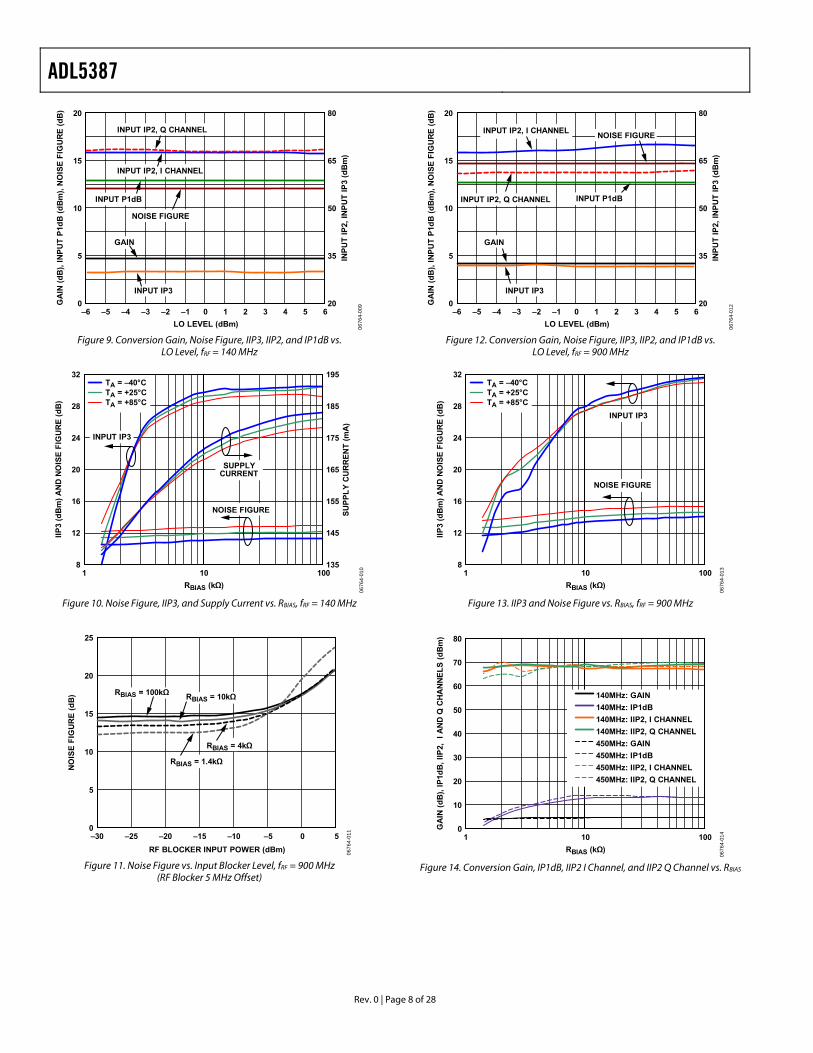
Figure 9. Conversion Gain, Noise Figure, IIP3, IIP2, and IP1dB vs.
LO Level, fRF = 140 MHz
32
28
24
20
16
12
81 10 100
IIP3
(dB
m) A
ND
NO
ISE
FIG
UR
E (d
B)
195
135
145
155
165
175
185
SUPP
LY C
UR
REN
T (m
A)
RBIAS (kΩ)
INPUT IP3
NOISE FIGURE
SUPPLYCURRENT
TA = +85°CTA = +25°CTA = –40°C
0676
4-01
0
Figure 10. Noise Figure, IIP3, and Supply Current vs. RBIAS, fRF = 140 MHz
25
20
15
10
5
0–30 50–5–10–15–20–25
NO
ISE
FIG
UR
E (d
B)
RF BLOCKER INPUT POWER (dBm)
RBIAS = 100kΩ RBIAS = 10kΩ
RBIAS = 4kΩ
RBIAS = 1.4kΩ
0676
4-01
1
Figure 11. Noise Figure vs. Input Blocker Level, fRF = 900 MHz
(RF Blocker 5 MHz Offset)
20
15
10
5
0–6 –5 –4 –3 –2 –1 0 1 2 3 4 5 6
GA
IN (d
B),
INPU
T P1
dB (d
Bm
), N
OIS
E FI
GU
RE
(dB
) 80
65
50
35
20
INPU
T IP
2, IN
PUT
IP3
(dB
m)
LO LEVEL (dBm)
INPUT IP2, I CHANNEL
INPUT P1dB
GAIN
INPUT IP3
NOISE FIGURE
INPUT IP2, Q CHANNEL
0676
4-01
2
Figure 12. Conversion Gain, Noise Figure, IIP3, IIP2, and IP1dB vs.
LO Level, fRF = 900 MHz
32
28
24
20
16
12
81 10
IIP3
(dB
m) A
ND
NO
ISE
FIG
UR
E (d
B)
RBIAS (kΩ)100
INPUT IP3
NOISE FIGURE
TA = +85°CTA = +25°CTA = –40°C
0676
4-01
3
Figure 13. IIP3 and Noise Figure vs. RBIAS, fRF = 900 MHz
80
70
60
50
40
30
20
10
01 10
GA
IN (d
B),
IP1d
B, I
IP2,
I A
ND
Q C
HA
NN
ELS
(dB
m)
RBIAS (kΩ)100
140MHz: GAIN140MHz: IP1dB140MHz: IIP2, I CHANNEL140MHz: IIP2, Q CHANNEL450MHz: GAIN450MHz: IP1dB450MHz: IIP2, I CHANNEL450MHz: IIP2, Q CHANNEL
0676
4-01
4
Figure 14. Conversion Gain, IP1dB, IIP2 I Channel, and IIP2 Q Channel vs. RBIAS
ADL5387
Rev. 0 | Page 9 of 28
35
30
25
20
15
10
50 5045403530252015105
IP1d
B, I
IP3
(dB
m)
80
50
55
60
65
70
75
INPU
T IP
2, I
AN
D Q
CH
AN
NEL
S (d
Bm
)
BB FREQUENCY (MHz)
–20
–30
–40
–50
–60
–70
–80
–90
–1000 200018001600140012001000800600400200
LO L
EAK
AG
E (d
Bm
)
INTERNAL 1xLO FREQUENCY (MHz)
TA = +85°CTA = +25°CTA = –40°C
IIP3 INPUT IP2,I CHANNEL
INPUT IP2,Q CHANNEL
IP1dB
1xLO
2xLO
0676
4-01
5
0676
4-01
8
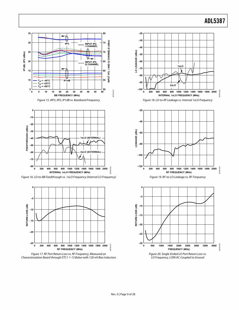
Figure 15. IIIP3, IIP2, IP1dB vs. Baseband Frequency
0
–10
–20
–30
–40
–50
–60
–70
–800 200018001600140012001000800600400200
FEED
THR
OU
GH
(dB
m)
INTERNAL 1xLO FREQUENCY (MHz)
1xLO (INTERNAL)
2xLO (EXTERNAL)
0676
4-01
6
Figure 16. LO-to-BB Feedthrough vs. 1xLO Frequency (Internal LO Frequency)
0
–25
–20
–15
–10
–5
0 200018001600140012001000800600400200
RET
UR
N L
OSS
(dB
)
RF FREQUENCY (MHz) 0676
4-01
7
Figure 17. RF Port Return Loss vs. RF Frequency, Measured on
Characterization Board through ETC1-1-13 Balun with 120 nH Bias Inductors
Figure 18. LO-to-RF Leakage vs. Internal 1xLO Frequency
–20
–40
–60
–80
–100
–1200 200018001600140012001000800600400200
LEA
KA
GE
(dB
c)
RF FREQUENCY (MHz) 0676
4-01
9
Figure 19. RF-to-LO Leakage vs. RF Frequency
0
–30
–25
–20
–15
–10
–5
0 4000350030002500200015001000500
RET
UR
N L
OSS
(dB
)
FREQUENCY (MHz) 0676
4-02
0
Figure 20. Single-Ended LO Port Return Loss vs.
LO Frequency, LOIN AC-Coupled to Ground
ADL5387
Rev. 0 | Page 10 of 28
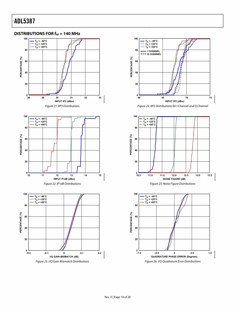
DISTRIBUTIONS FOR fRF = 140 MHz 100
0
20
40
60
80
28 333029 3231
PER
CEN
TAG
E (%
)
INPUT IP3 (dBm)
TA = +85°CTA = +25°CTA = –40°C
0676
4-02
1
Figure 21. IIP3 Distributions
100
0
20
40
60
80
10 151211 1413
PER
CEN
TAG
E (%
)
INPUT P1dB (dBm)
TA = +85°CTA = +25°CTA = –40°C
0676
4-02
2
Figure 22. IP1dB Distributions
100
0
20
40
60
80
–0.2 0.20–0.1 0.1
PER
CEN
TAG
E (%
)
I/Q GAIN MISMATCH (dB)
TA = +85°CTA = +25°CTA = –40°C
0676
4-02
3
Figure 23. I/Q Gain Mismatch Distributions
100
0
20
40
60
80
60 7565 70
PER
CEN
TAG
E (%
)
INPUT IP2 (dBm)
TA = +85°CTA = +25°CTA = –40°C
Q CHANNELI CHANNEL
0676
4-02
4
Figure 24. IIP2 Distributions for I Channel and Q Channel
100
0
20
40
60
80
10.5 13.513.012.512.011.511.0
PER
CEN
TAG
E (%
)
NOISE FIGURE (dB)
TA = +85°CTA = +25°CTA = –40°C
0676
4-02
5
Figure 25. Noise Figure Distributions
100
0
20
40
60
80
–1.0 1.00.50–0.5
PER
CEN
TAG
E (%
)
QUADRATURE PHASE ERROR (Degrees)
TA = +85°CTA = +25°CTA = –40°C
0676
4-02
6
Figure 26. I/Q Quadrature Error Distributions
ADL5387
Rev. 0 | Page 11 of 28
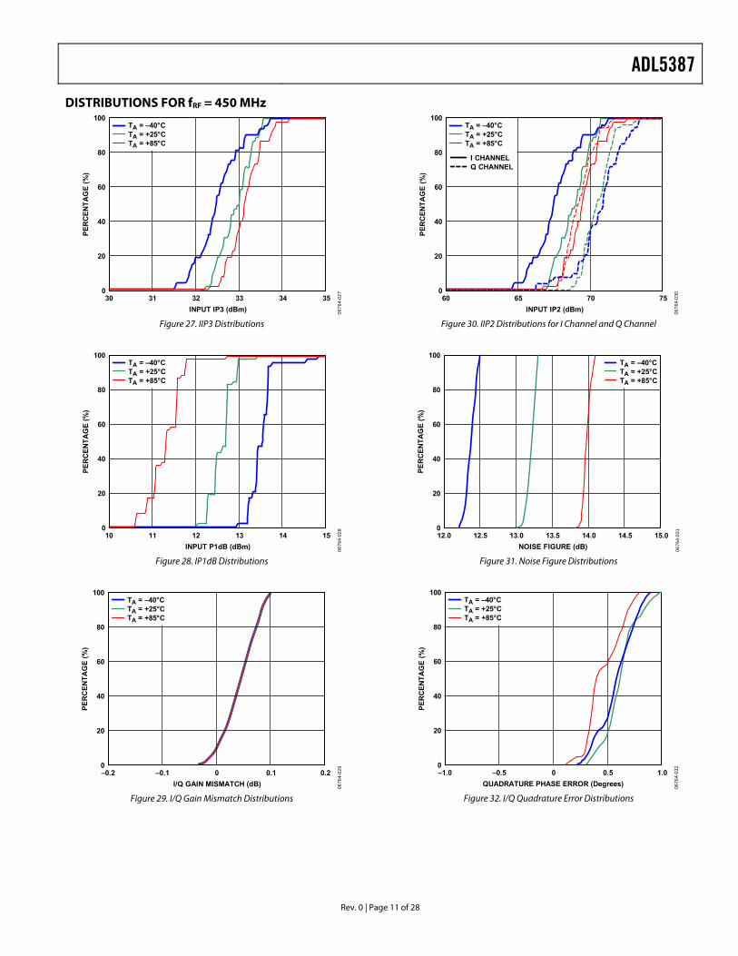
DISTRIBUTIONS FOR fRF = 450 MHz 100
0
20
40
60
80
30 3534333231
PER
CEN
TAG
E (%
)
INPUT IP3 (dBm)
TA = +85°CTA = +25°CTA = –40°C
0676
4-02
7
Figure 27. IIP3 Distributions
100
0
20
40
60
80
10 1514131211
PER
CEN
TAG
E (%
)
INPUT P1dB (dBm)
TA = +85°CTA = +25°CTA = –40°C
0676
4-02
8
Figure 28. IP1dB Distributions
100
0
20
40
60
80
–0.2 0.20.10–0.1
PER
CEN
TAG
E (%
)
I/Q GAIN MISMATCH (dB)
TA = +85°CTA = +25°CTA = –40°C
0676
4-02
9
Figure 29. I/Q Gain Mismatch Distributions
100
0
20
40
60
80
60 7565 70
PER
CEN
TAG
E (%
)
INPUT IP2 (dBm)
TA = +85°CTA = +25°CTA = –40°C
Q CHANNELI CHANNEL
0676
4-03
0
Figure 30. IIP2 Distributions for I Channel and Q Channel
100
0
20
40
60
80
12.0 15.014.514.013.513.012.5
PER
CEN
TAG
E (%
)
NOISE FIGURE (dB)
TA = +85°CTA = +25°CTA = –40°C
0676
4-03
1
Figure 31. Noise Figure Distributions
100
0
20
40
60
80
–1.0 –0.5 0 0.5 1.0
PER
CEN
TAG
E (%
)
QUADRATURE PHASE ERROR (Degrees)
TA = +85°CTA = +25°CTA = –40°C
0676
4-03
2
Figure 32. I/Q Quadrature Error Distributions
ADL5387
Rev. 0 | Page 12 of 28
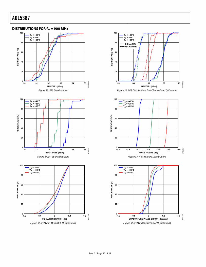
DISTRIBUTIONS FOR fRF = 900 MHz 100
0
20
40
60
80
30 31 3332 34 35
PER
CEN
TAG
E (%
)
INPUT IP3 (dBm)
TA = +85°CTA = +25°CTA = –40°C
0676
4-03
3
Figure 33. IIP3 Distributions
100
0
20
40
60
80
10 11 1312 14 15
PER
CEN
TAG
E (%
)
INPUT P1dB (dBm)
TA = +85°CTA = +25°CTA = –40°C
0676
4-03
4
Figure 34. IP1dB Distributions
100
0
20
40
60
80
–0.2 –0.1 0 0.1 0.2
PER
CEN
TAG
E (%
)
I/Q GAIN MISMATCH (dB)
TA = +85°CTA = +25°CTA = –40°C
0676
4-03
5
Figure 35. I/Q Gain Mismatch Distributions
100
0
20
40
60
80
55 756560 70
PER
CEN
TAG
E (%
)
INPUT IP2 (dBm)
TA = +85°CTA = +25°CTA = –40°C
Q CHANNELI CHANNEL
0676
4-03
6
Figure 36. IIP2 Distributions for I Channel and Q Channel
100
0
20
40
60
80
13.0 13.5 14.0 14.5 15.0 15.5 16.0
PER
CEN
TAG
E (%
)
NOISE FIGURE (dB)
TA = +85°CTA = +25°CTA = –40°C
0676
4-03
7
Figure 37. Noise Figure Distributions
100
0
20
40
60
80
–1.0 1.00.50–0.5
PER
CEN
TAG
E (%
)
QUADRATURE PHASE ERROR (Degrees)
TA = +85°CTA = +25°CTA = –40°C
0676
4-03
8
Figure 38. I/Q Quadrature Error Distributions
ADL5387
Rev. 0 | Page 13 of 28
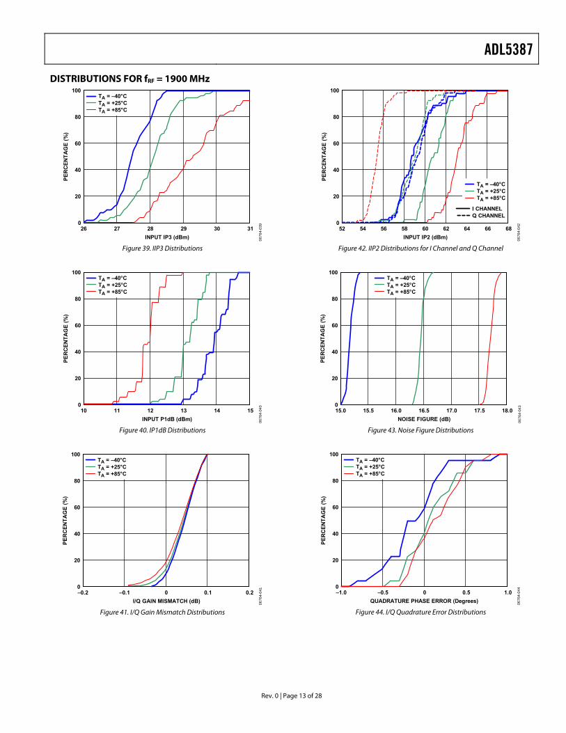
DISTRIBUTIONS FOR fRF = 1900 MHz 100
0
20
40
60
80
26 3129 302827
PER
CEN
TAG
E (%
)
INPUT IP3 (dBm)
TA = +85°CTA = +25°CTA = –40°C
0676
4-03
9
Figure 39. IIP3 Distributions
100
0
20
40
60
80
10 1513 141211
PER
CEN
TAG
E (%
)
INPUT P1dB (dBm)
TA = +85°CTA = +25°CTA = –40°C
0676
4-04
0
Figure 40. IP1dB Distributions
100
0
20
40
60
80
–0.2 0.20.10–0.1
PER
CEN
TAG
E (%
)
I/Q GAIN MISMATCH (dB)
TA = +85°CTA = +25°CTA = –40°C
0676
4-04
1
Figure 41. I/Q Gain Mismatch Distributions
100
0
20
40
60
80
52 6866646260585654
PER
CEN
TAG
E (%
)
INPUT IP2 (dBm)
TA = +85°CTA = +25°CTA = –40°C
Q CHANNELI CHANNEL
0676
4-04
2
Figure 42. IIP2 Distributions for I Channel and Q Channel
100
0
20
40
60
80
15.0 18.017.517.016.516.015.5
PER
CEN
TAG
E (%
)
NOISE FIGURE (dB)
TA = +85°CTA = +25°CTA = –40°C
0676
4-04
3
Figure 43. Noise Figure Distributions
100
0
20
40
60
80
–1.0 1.00.50–0.5
PER
CEN
TAG
E (%
)
QUADRATURE PHASE ERROR (Degrees)
TA = +85°CTA = +25°CTA = –40°C
0676
4-04
4
Figure 44. I/Q Quadrature Error Distributions
ADL5387
Rev. 0 | Page 14 of 28
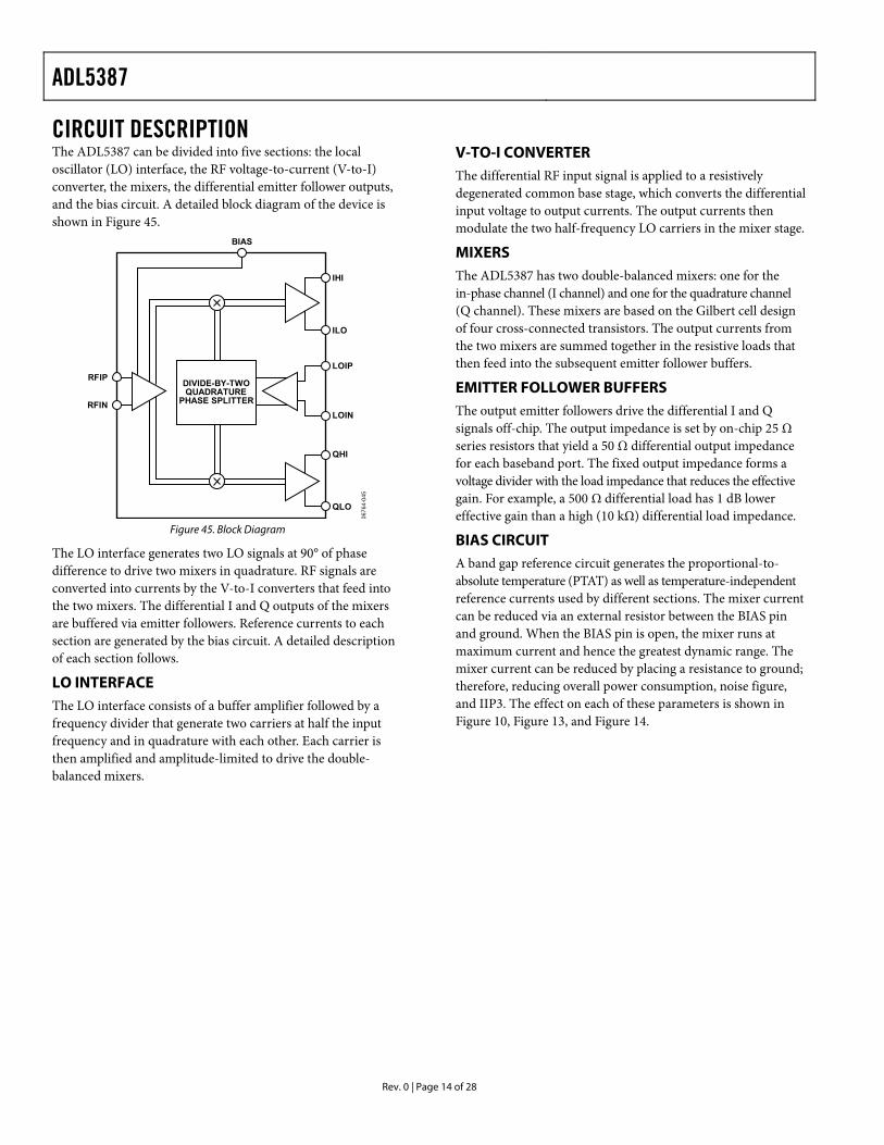
CIRCUIT DESCRIPTION The ADL5387 can be divided into five sections: the local oscillator (LO) interface, the RF voltage-to-current (V-to-I) converter, the mixers, the differential emitter follower outputs, and the bias circuit. A detailed block diagram of the device is shown in Figure 45.
RFIP
RFIN
BIAS
DIVIDE-BY-TWOQUADRATURE
PHASE SPLITTER
IHI
ILO
LOIP
LOIN
QHI
QLO
0676
4-04
5
Figure 45. Block Diagram
The LO interface generates two LO signals at 90° of phase difference to drive two mixers in quadrature. RF signals are converted into currents by the V-to-I converters that feed into the two mixers. The differential I and Q outputs of the mixers are buffered via emitter followers. Reference currents to each section are generated by the bias circuit. A detailed description of each section follows.
LO INTERFACE The LO interface consists of a buffer amplifier followed by a frequency divider that generate two carriers at half the input frequency and in quadrature with each other. Each carrier is then amplified and amplitude-limited to drive the double-balanced mixers.
V-TO-I CONVERTER The differential RF input signal is applied to a resistively degenerated common base stage, which converts the differential input voltage to output currents. The output currents then modulate the two half-frequency LO carriers in the mixer stage.
MIXERS The ADL5387 has two double-balanced mixers: one for the in-phase channel (I channel) and one for the quadrature channel (Q channel). These mixers are based on the Gilbert cell design of four cross-connected transistors. The output currents from the two mixers are summed together in the resistive loads that then feed into the subsequent emitter follower buffers.
EMITTER FOLLOWER BUFFERS The output emitter followers drive the differential I and Q signals off-chip. The output impedance is set by on-chip 25 Ω series resistors that yield a 50 Ω differential output impedance for each baseband port. The fixed output impedance forms a voltage divider with the load impedance that reduces the effective gain. For example, a 500 Ω differential load has 1 dB lower effective gain than a high (10 kΩ) differential load impedance.
BIAS CIRCUIT A band gap reference circuit generates the proportional-to-absolute temperature (PTAT) as well as temperature-independent reference currents used by different sections. The mixer current can be reduced via an external resistor between the BIAS pin and ground. When the BIAS pin is open, the mixer runs at maximum current and hence the greatest dynamic range. The mixer current can be reduced by placing a resistance to ground; therefore, reducing overall power consumption, noise figure, and IIP3. The effect on each of these parameters is shown in Figure 10, Figure 13, and Figure 14.
ADL5387
Rev. 0 | Page 15 of 28
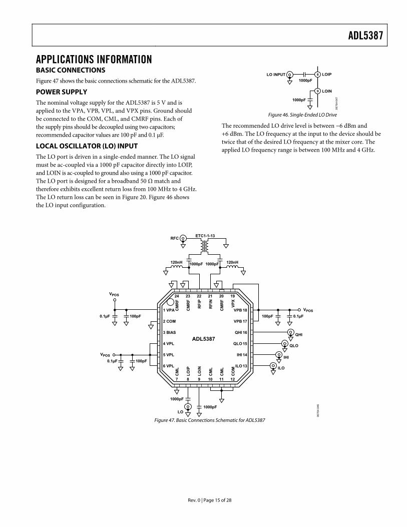
APPLICATIONS INFORMATION BASIC CONNECTIONS Figure 47 shows the basic connections schematic for the ADL5387.
POWER SUPPLY The nominal voltage supply for the ADL5387 is 5 V and is applied to the VPA, VPB, VPL, and VPX pins. Ground should be connected to the COM, CML, and CMRF pins. Each of the supply pins should be decoupled using two capacitors; recommended capacitor values are 100 pF and 0.1 μF.
LOCAL OSCILLATOR (LO) INPUT The LO port is driven in a single-ended manner. The LO signal must be ac-coupled via a 1000 pF capacitor directly into LOIP, and LOIN is ac-coupled to ground also using a 1000 pF capacitor. The LO port is designed for a broadband 50 Ω match and therefore exhibits excellent return loss from 100 MHz to 4 GHz. The LO return loss can be seen in Figure 20. Figure 46 shows the LO input configuration.
LO INPUT LOIP
LOIN
1000pF
1000pF
8
9
0676
4-04
7
Figure 46. Single-Ended LO Drive
The recommended LO drive level is between −6 dBm and +6 dBm. The LO frequency at the input to the device should be twice that of the desired LO frequency at the mixer core. The applied LO frequency range is between 100 MHz and 4 GHz.
RFC
120nH 120nH1000pF 1000pF
100pF 100pF0.1µF
1000pF
100pF
1000pF
0.1µF
0.1µF
VPOS
VPOS
LO
VPOS
ETC1-1-13
1
ADL5387
CM
RF
CM
RF
RFI
P
RFI
N
CM
RF
VPX
CM
L
LOIP
LOIN
CM
L
CM
L
CO
M
24 23 22 21 20 19
7 8 9 10 11 12
2
3
4
5
6
VPA
COM
BIAS
VPL
VPL
VPL
18
17
16
15
14
13
VPB
QHI
QLO
IHI
ILO
VPB
QHI
QLO
IHI
ILO
0676
4-04
6
Figure 47. Basic Connections Schematic for ADL5387

ADL5387
Rev. 0 | Page 16 of 28
RF INPUT The RF inputs have a differential input impedance of approximately 50 Ω. For optimum performance, the RF port should be driven differentially through a balun. The recommended balun is M/A-COM ETC1-1-13. The RF inputs to the device should be ac-coupled with 1000 pF capacitors. Ground-referenced choke inductors must also be connected to RFIP and RFIN (recommended value = 120 nH, Coilcraft 0402CS-R12XJL) for appropriate biasing. Several important aspects must be taken into account when selecting an appropriate choke inductor for this application. First, the inductor must be able to handle the approximately 40 mA of standing dc current being delivered from each of the RF input pins (RFIP, RFIN). (The suggested 0402 inductor has a 50 mA current rating). The purpose of the choke inductors is to provide a very low resistance dc path to ground and high ac impedance at the RF frequency so as not to affect the RF input impedance. A choke inductor that has a self-resonant frequency greater than the RF input frequency ensures that the choke is still looking inductive and therefore has a more predictable ac impedance (jωL) at the RF frequency. Figure 48 shows the RF input configuration.
RF INPUT
RFIN
ETC1-1-13
120nH
120nH
RFIP
1000pF
1000pF
21
22
0676
4-04
8
Figure 48. RF Input
The differential RF port return loss has been characterized as shown in Figure 49.
–10
–12
–14
–16
–18
–20
–22
–24
–26
–280 0.2 0.4 0.6 0.8 1.0 1.2 1.4 1.6 1.8 2.0
S(1,
1) (
dB)
FREQUENCY (GHz) 0676
4-04
9
Figure 49. Differential RF Port Return Loss
BASEBAND OUTPUTS The baseband outputs QHI, QLO, IHI, and ILO are fixed impedance ports. Each baseband pair has a 50 Ω differential output impedance. The outputs can be presented with differential loads as low as 200 Ω (with some degradation in linearity and gain) or high impedance differential loads (500 Ω or greater impedance yields the same excellent linearity) that is typical of an ADC. The TCM9-1 9:1 balun converts the differential IF output to single-ended. When loaded with 50 Ω, this balun presents a 450 Ω load to the device. The typical maximum linear voltage swing for these outputs is 2 V p-p differential. The bias level on these pins is equal to VPOS − 2.8 V. The output 3 dB bandwidth is 240 MHz. Figure 50 shows the baseband output configuration.
QHI
QLO
IHI
ILO
QHI
QLO
IHI
ILO
16
15
14
13
0676
4-05
0
Figure 50. Baseband Output Configuration
ADL5387
Rev. 0 | Page 17 of 28
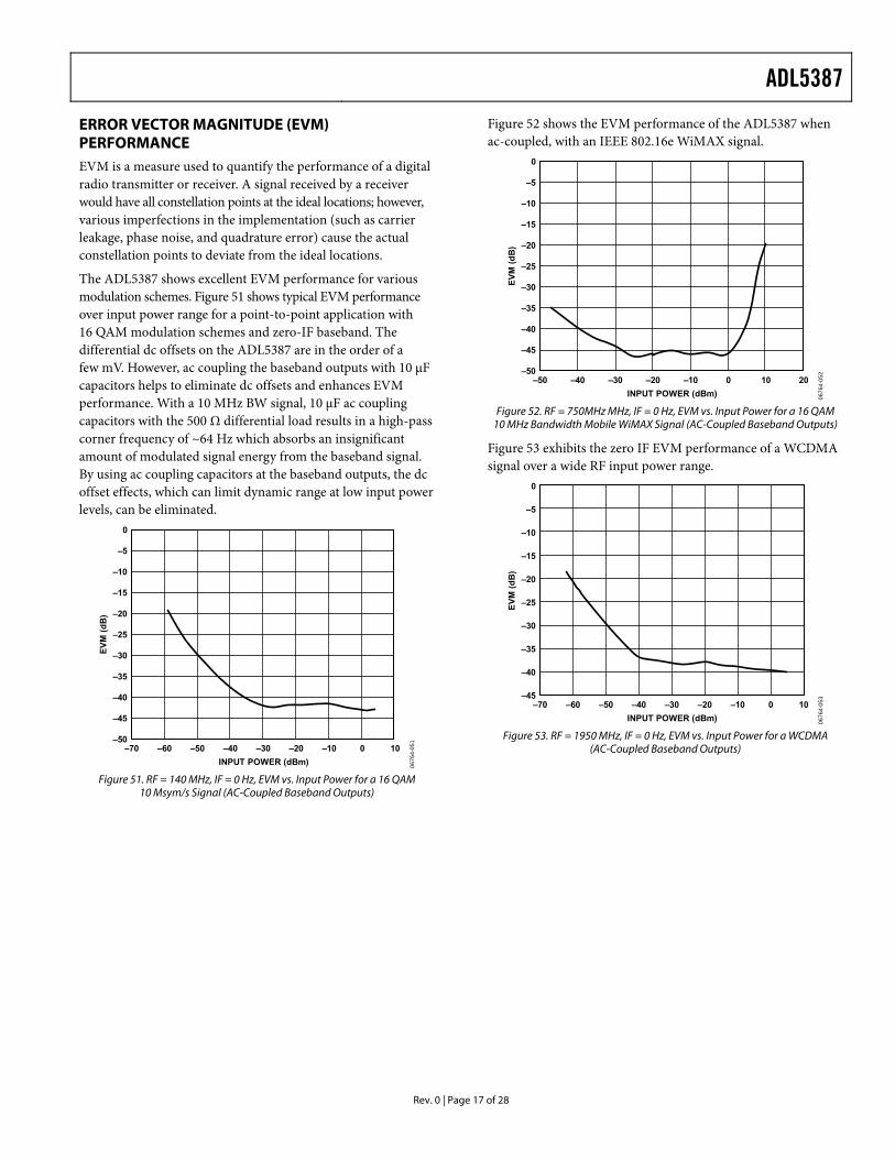
ERROR VECTOR MAGNITUDE (EVM) PERFORMANCE EVM is a measure used to quantify the performance of a digital radio transmitter or receiver. A signal received by a receiver would have all constellation points at the ideal locations; however, various imperfections in the implementation (such as carrier leakage, phase noise, and quadrature error) cause the actual constellation points to deviate from the ideal locations.
The ADL5387 shows excellent EVM performance for various modulation schemes. Figure 51 shows typical EVM performance over input power range for a point-to-point application with 16 QAM modulation schemes and zero-IF baseband. The differential dc offsets on the ADL5387 are in the order of a few mV. However, ac coupling the baseband outputs with 10 μF capacitors helps to eliminate dc offsets and enhances EVM performance. With a 10 MHz BW signal, 10 μF ac coupling capacitors with the 500 Ω differential load results in a high-pass corner frequency of ~64 Hz which absorbs an insignificant amount of modulated signal energy from the baseband signal. By using ac coupling capacitors at the baseband outputs, the dc offset effects, which can limit dynamic range at low input power levels, can be eliminated.
0
–50
–45
–40
–35
–30
–25
–20
–15
–10
–5
–70 100–10–20–30–40–50–60
EVM
(dB
)
INPUT POWER (dBm) 0676
4-05
1
Figure 51. RF = 140 MHz, IF = 0 Hz, EVM vs. Input Power for a 16 QAM
10 Msym/s Signal (AC-Coupled Baseband Outputs)
Figure 52 shows the EVM performance of the ADL5387 when ac-coupled, with an IEEE 802.16e WiMAX signal.
0
–50
–45
–40
–35
–30
–25
–20
–15
–10
–5
–50 20100–10–20–30–40
EVM
(dB
)
INPUT POWER (dBm) 0676
4-05
2
Figure 52. RF = 750MHz MHz, IF = 0 Hz, EVM vs. Input Power for a 16 QAM
10 MHz Bandwidth Mobile WiMAX Signal (AC-Coupled Baseband Outputs)
Figure 53 exhibits the zero IF EVM performance of a WCDMA signal over a wide RF input power range.
0
–45
–40
–35
–30
–25
–20
–15
–10
–5
–70 –60 100–10–20–30–40–50
EVM
(dB
)
INPUT POWER (dBm) 0676
4-05
3
Figure 53. RF = 1950 MHz, IF = 0 Hz, EVM vs. Input Power for a WCDMA
(AC-Coupled Baseband Outputs)
ADL5387
Rev. 0 | Page 18 of 28
0676
4-05
4
0°
0°
SINωLOt
COSωLOt
ωIF ωIF
ωLSB ωUSB
–ωIF 0 +ωIF0 +ωIF
0 +ωIF–ωIF 0 +ωIF
ωLO
–90°
+90°
Figure 54. Illustration of the Image Problem
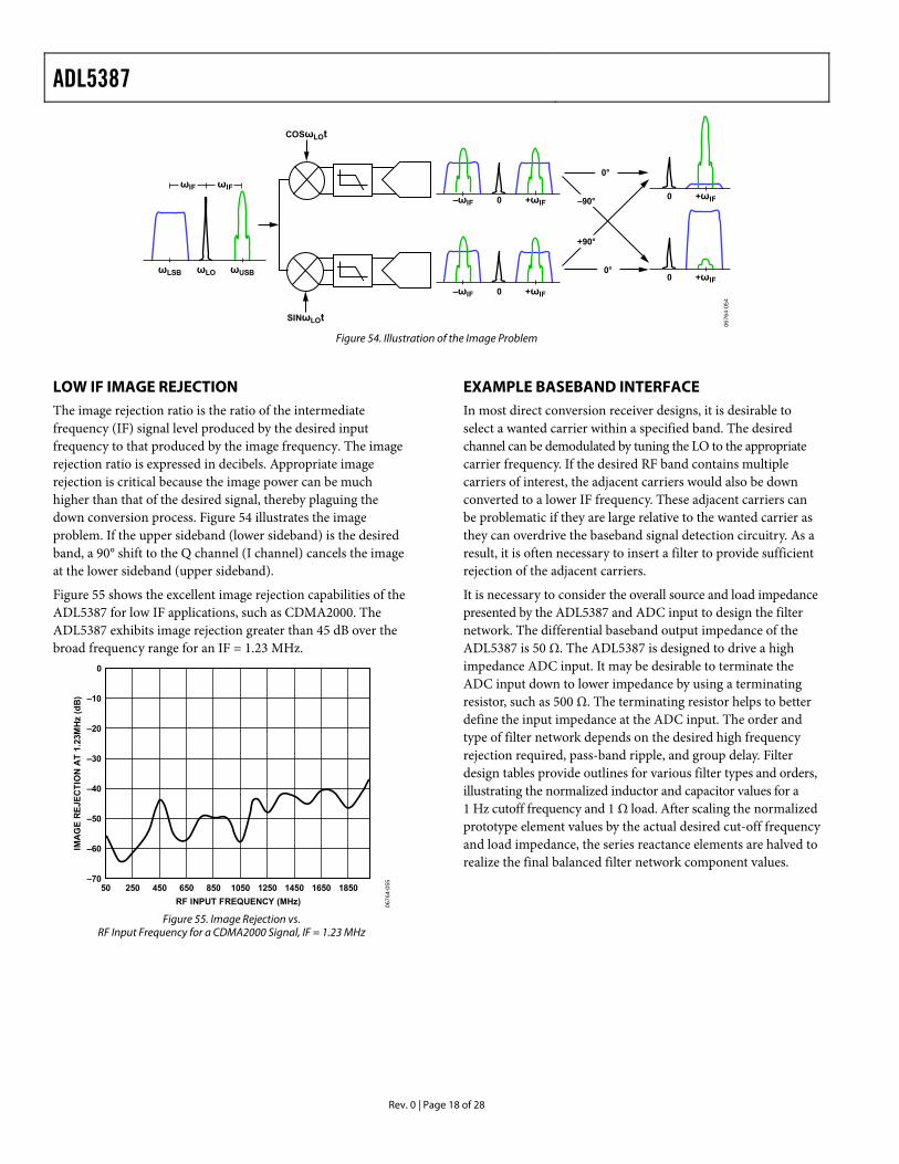
LOW IF IMAGE REJECTION The image rejection ratio is the ratio of the intermediate frequency (IF) signal level produced by the desired input frequency to that produced by the image frequency. The image rejection ratio is expressed in decibels. Appropriate image rejection is critical because the image power can be much higher than that of the desired signal, thereby plaguing the down conversion process. Figure 54 illustrates the image problem. If the upper sideband (lower sideband) is the desired band, a 90° shift to the Q channel (I channel) cancels the image at the lower sideband (upper sideband).
Figure 55 shows the excellent image rejection capabilities of the ADL5387 for low IF applications, such as CDMA2000. The ADL5387 exhibits image rejection greater than 45 dB over the broad frequency range for an IF = 1.23 MHz.
0
–70
–60
–50
–40
–30
–20
–10
50 250 450 650 850 1050 1250 1450 1650 1850
IMA
GE
REJ
ECTI
ON
AT
1.23
MH
z (d
B)
RF INPUT FREQUENCY (MHz) 0676
4-05
5
Figure 55. Image Rejection vs.
RF Input Frequency for a CDMA2000 Signal, IF = 1.23 MHz
EXAMPLE BASEBAND INTERFACE In most direct conversion receiver designs, it is desirable to select a wanted carrier within a specified band. The desired channel can be demodulated by tuning the LO to the appropriate carrier frequency. If the desired RF band contains multiple carriers of interest, the adjacent carriers would also be down converted to a lower IF frequency. These adjacent carriers can be problematic if they are large relative to the wanted carrier as they can overdrive the baseband signal detection circuitry. As a result, it is often necessary to insert a filter to provide sufficient rejection of the adjacent carriers.
It is necessary to consider the overall source and load impedance presented by the ADL5387 and ADC input to design the filter network. The differential baseband output impedance of the ADL5387 is 50 Ω. The ADL5387 is designed to drive a high impedance ADC input. It may be desirable to terminate the ADC input down to lower impedance by using a terminating resistor, such as 500 Ω. The terminating resistor helps to better define the input impedance at the ADC input. The order and type of filter network depends on the desired high frequency rejection required, pass-band ripple, and group delay. Filter design tables provide outlines for various filter types and orders, illustrating the normalized inductor and capacitor values for a 1 Hz cutoff frequency and 1 Ω load. After scaling the normalized prototype element values by the actual desired cut-off frequency and load impedance, the series reactance elements are halved to realize the final balanced filter network component values.

ADL5387
Rev. 0 | Page 19 of 28
As an example, a second-order, Butterworth, low-pass filter design is shown in Figure 56 where the differential load impedance is 500 Ω, and the source impedance of the ADL5387 is 50 Ω. The normalized series inductor value for the 10-to-1, load-to-source impedance ratio is 0.074 H, and the normalized shunt capacitor is 14.814 F. For a 10.9 MHz cutoff frequency, the single-ended equivalent circuit consists of a 0.54 μH series inductor followed by a 433 pF shunt capacitor.
The balanced configuration is realized as the 0.54 μH inductor is split in half to realize the network shown in Figure 56.
0676
4-05
6
VS
RS2
RSRL
RS2
RL2
RL2
433pF
VS
RS = 50Ω
RL= 500Ω
0.54µH
0.27µH
0.27µH
433pF
BALANCEDCONFIGURATION
DENORMALIZEDSINGLE-ENDED
EQUIVALENT
VS
RS = 50Ω
= 0.1
RL= 500Ω
LN = 0.074H
CN 14.814FNORMALIZED
SINGLE-ENDEDCONFIGURATION
= 25Ω
= 25Ω
= 250Ω
= 250Ω
fC = 10.9MHz
fC = 1Hz
Figure 56. Second-Order, Butterworth, Low-Pass Filter Design Example
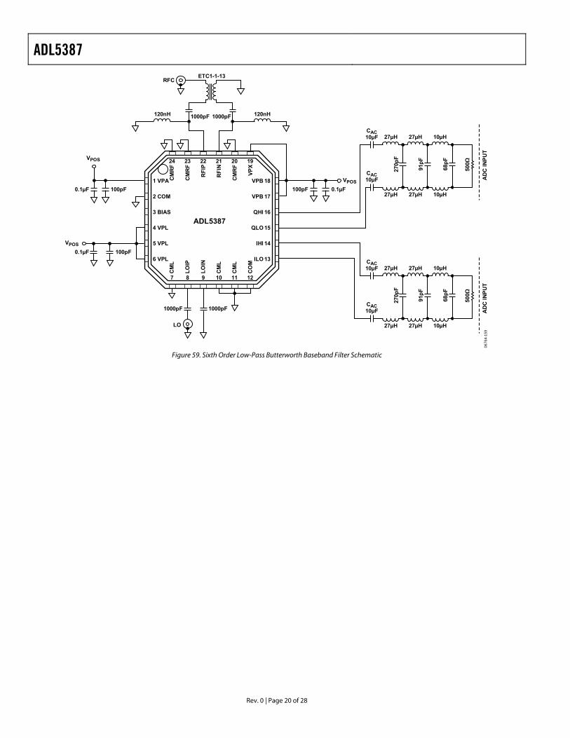
A complete design example is shown in Figure 59. A sixth-order Butterworth differential filter having a 1.9 MHz corner frequency interfaces the output of the ADL5387 to that of an ADC input. The 500 Ω load resistor defines the input impedance of the ADC. The filter adheres to typical direct conversion WCDMA applications, where 1.92 MHz away from the carrier IF frequency, 1 dB of rejection is desired and 2.7 MHz away 10 dB of rejection is desired.
Figure 57 and Figure 58 show the measured frequency response and group delay of the filter.
10
5
–20
–15
–10
–5
0
0 33.02.52.01.51.00.5
MA
GN
ITU
DE
RES
PON
SE (d
B)
FREQUENCY (MHz) 0676
4-15
7
.5
Figure 57. Baseband Filter Response
900
800
700
600
500
400
300
200
1000 0.2 0.4 0.6 0.8 1.0 1.2 1.4 1.6 1.8
DEL
AY
(ns)
FREQUENCY (MHz) 0676
4-15
8
Figure 58. Baseband Filter Group Delay
ADL5387
Rev. 0 | Page 20 of 28
0676
4-15
9
RFC
1000pF
100pF 0.1µF
1000pF
100pF0.1µF
0.1µF 100pF
VPOS
VPOS
LO
1000pF1000pF
VPOS
ETC1-1-13
1
ADL5387
CM
RF
CM
RF
RFI
P
RFI
N
CM
RF
VPX
CM
L
LOIP
LOIN
CM
L
CM
L
CO
M
24 23 22 21 20 19
7 8 9 10 11 12
2
3
4
5
6
VPA
COM
BIAS
VPL
VPL
VPL
18
17
16
15
14
13
VPB
VPB
QHI
QLO
IHI
ILO
120nH 120nH
CAC10µF
CAC10µF
27µH
27µH
270p
F
27µH
27µH
91pF
10µH
10µH
68pF
500Ω
CAC10µF
CAC10µF
27µH
27µH
270p
F
27µH
27µH
91pF
10µH
10µH
68pF
500Ω
AD
C IN
PUT
AD
C IN
PUT
Figure 59. Sixth Order Low-Pass Butterworth Baseband Filter Schematic
ADL5387
Rev. 0 | Page 21 of 28
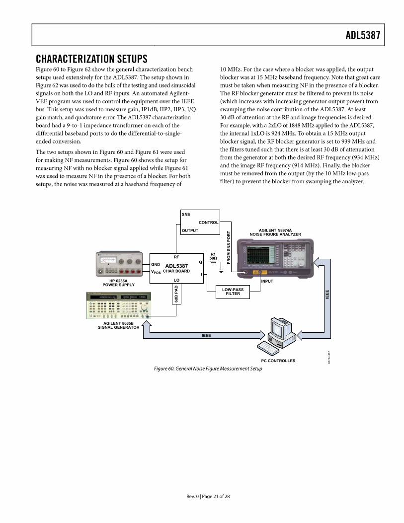
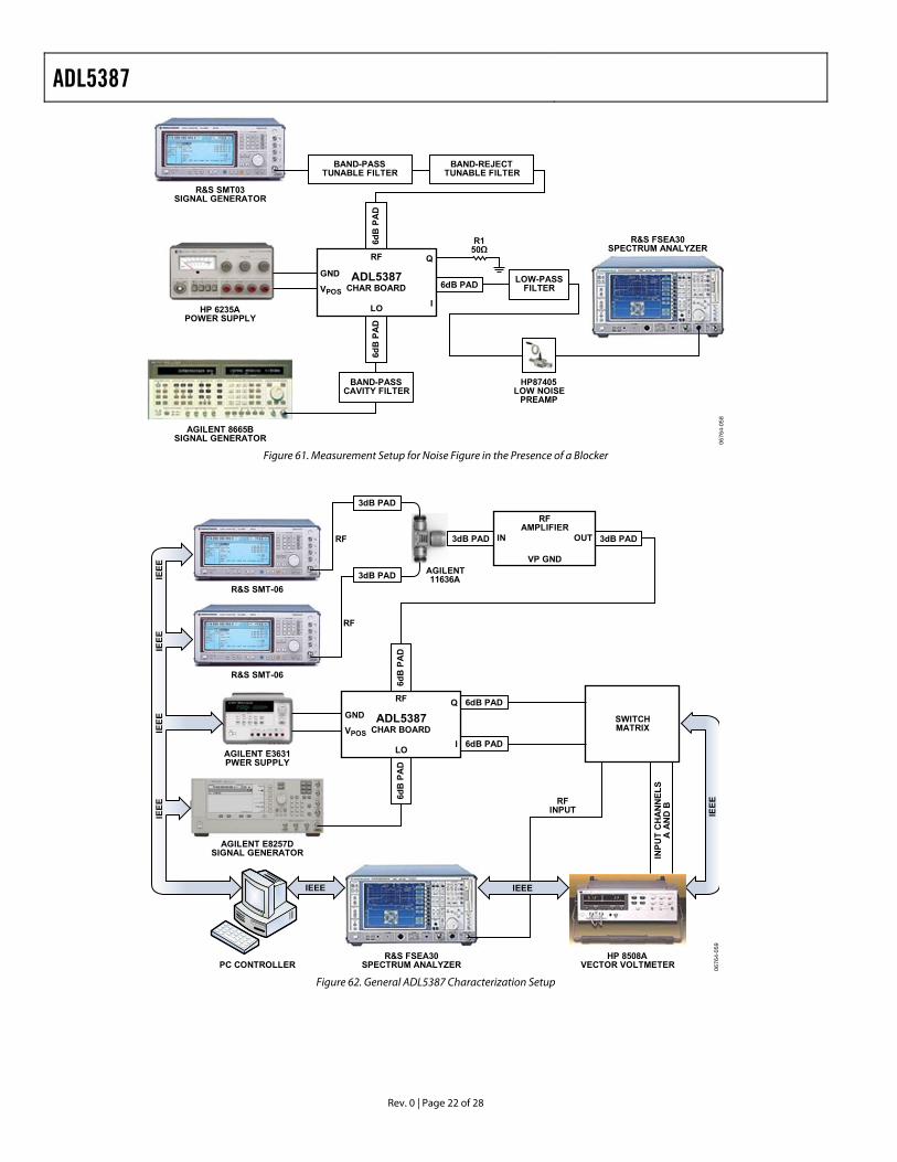
CHARACTERIZATION SETUPS Figure 60 to Figure 62 show the general characterization bench setups used extensively for the ADL5387. The setup shown in Figure 62 was used to do the bulk of the testing and used sinusoidal signals on both the LO and RF inputs. An automated Agilent-VEE program was used to control the equipment over the IEEE bus. This setup was used to measure gain, IP1dB, IIP2, IIP3, I/Q gain match, and quadrature error. The ADL5387 characterization board had a 9-to-1 impedance transformer on each of the differential baseband ports to do the differential-to-single-ended conversion.
The two setups shown in Figure 60 and Figure 61 were used for making NF measurements. Figure 60 shows the setup for measuring NF with no blocker signal applied while Figure 61 was used to measure NF in the presence of a blocker. For both setups, the noise was measured at a baseband frequency of
10 MHz. For the case where a blocker was applied, the output blocker was at 15 MHz baseband frequency. Note that great care must be taken when measuring NF in the presence of a blocker. The RF blocker generator must be filtered to prevent its noise (which increases with increasing generator output power) from swamping the noise contribution of the ADL5387. At least 30 dB of attention at the RF and image frequencies is desired. For example, with a 2xLO of 1848 MHz applied to the ADL5387, the internal 1xLO is 924 MHz. To obtain a 15 MHz output blocker signal, the RF blocker generator is set to 939 MHz and the filters tuned such that there is at least 30 dB of attenuation from the generator at both the desired RF frequency (934 MHz) and the image RF frequency (914 MHz). Finally, the blocker must be removed from the output (by the 10 MHz low-pass filter) to prevent the blocker from swamping the analyzer.
HP 6235APOWER SUPPLY
AGILENT 8665BSIGNAL GENERATOR
IEEE
IEEE
PC CONTROLLER
CONTROL
SNS
OUTPUT AGILENT N8974ANOISE FIGURE ANALYZER
6dB
PA
D
ADL5387CHAR BOARD
RF
LO
Q
I
GND
VPOS
LOW-PASSFILTER
INPUT
R150Ω
FRO
M S
NS
POR
T
0676
4-05
7
Figure 60. General Noise Figure Measurement Setup
ADL5387
Rev. 0 | Page 22 of 28
R&S FSEA30SPECTRUM ANALYZER
HP 6235APOWER SUPPLY
AGILENT 8665BSIGNAL GENERATOR
LOW-PASSFILTER
R&S SMT03SIGNAL GENERATOR
ADL5387CHAR BOARD
RF
LO
Q
I
GND
VPOS
6dB
PA
D
6dB PAD
6dB
PA
D
R150Ω
BAND-PASSCAVITY FILTER
BAND-PASSTUNABLE FILTER
BAND-REJECTTUNABLE FILTER
HP87405LOW NOISE
PREAMP
0676
4-05
8
Figure 61. Measurement Setup for Noise Figure in the Presence of a Blocker
0676
4-05
9
R&S FSEA30SPECTRUM ANALYZER
HP 8508AVECTOR VOLTMETER
R&S SMT-06
AGILENT E3631PWER SUPPLY
AGILENT E8257DSIGNAL GENERATOR
PC CONTROLLER
R&S SMT-06
IEEE
IEEE
IEEE
IEEE
IEEE IEEE
ADL5387CHAR BOARD
RF
LO
Q
I
GND
VPOS
6dB
PA
D
6dB PAD
6dB PAD
6dB
PA
D
SWITCHMATRIX
RFAMPLIFIER
VP GND
OUTIN 3dB PAD3dB PAD
3dB PAD
3dB PAD
RF
RF
AGILENT11636A
INPU
T C
HA
NN
ELS
A A
ND
B
RFINPUT IE
EE
Figure 62. General ADL5387 Characterization Setup
ADL5387
Rev. 0 | Page 23 of 28
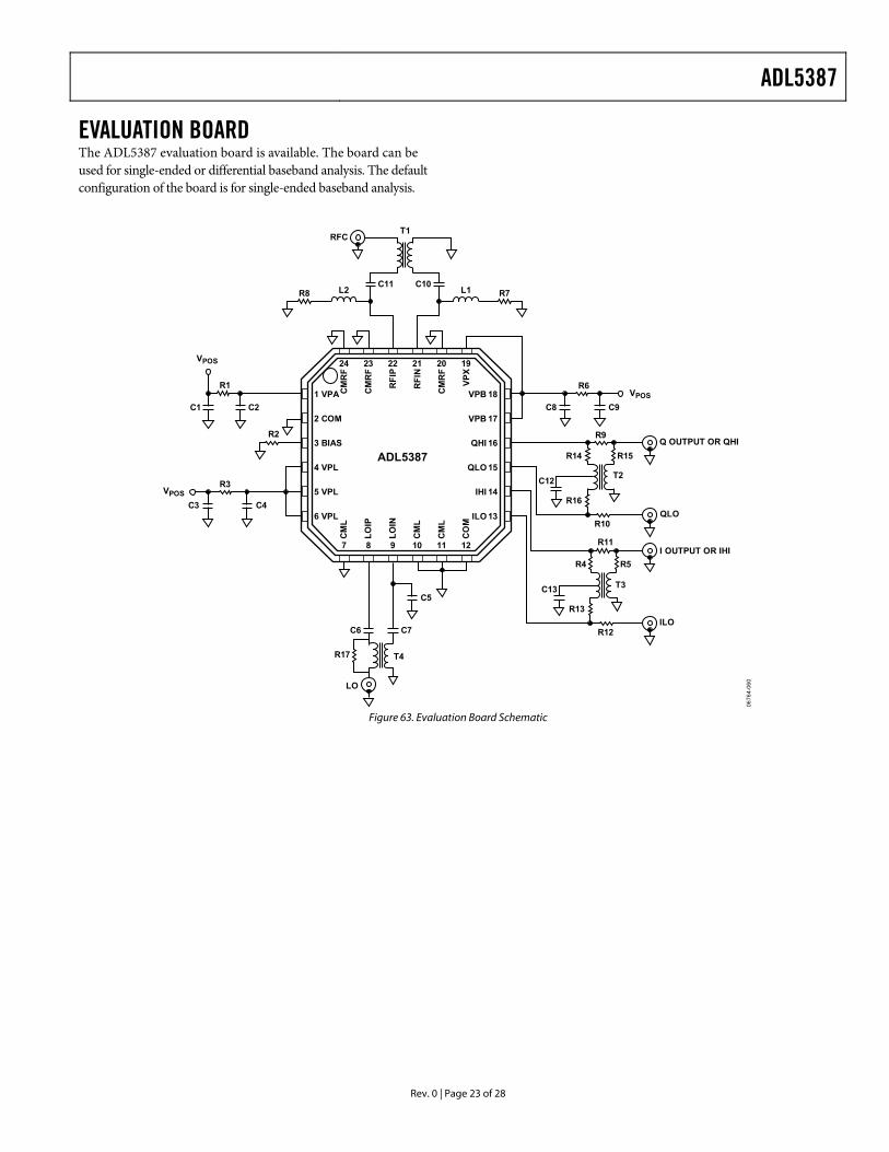
EVALUATION BOARD The ADL5387 evaluation board is available. The board can be used for single-ended or differential baseband analysis. The default configuration of the board is for single-ended baseband analysis.
RFC
C11
C8
R14
R16
R10
C12
R15
T2
T3
R9
R11
C9
C10
C2C1
C3 C4
R1
R2
VPOS
VPOS
LO
C5
C7C6
R17
VPOS
T1
T4
1
ADL5387
CM
RF
CM
RF
RFI
P
RFI
N
CM
RF
VPX
CM
L
LOIP
LOIN
CM
L
CM
L
CO
M
24 23 22 21 20 19
7 8 9 10 11 12
2
3
4
5
6
VPA
COM
BIAS
VPL
VPL
VPL
18
17
16
15
14
13
VPB
Q OUTPUT OR QHI
QLO
I OUTPUT OR IHI
ILO
VPB
QHI
QLO
IHI
ILO
R8 R7L2 L1
R6
R3
R4
R13
C13
R5
R12
0676
4-06
0
Figure 63. Evaluation Board Schematic
ADL5387
Rev. 0 | Page 24 of 28
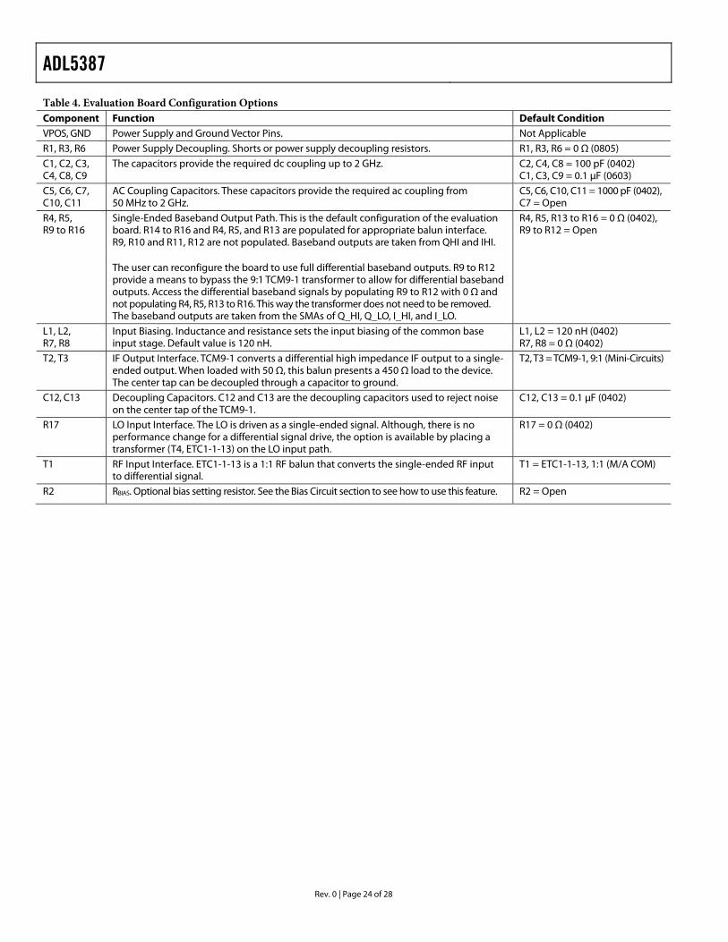
Table 4. Evaluation Board Configuration Options Component Function Default Condition VPOS, GND Power Supply and Ground Vector Pins. Not Applicable R1, R3, R6 Power Supply Decoupling. Shorts or power supply decoupling resistors. R1, R3, R6 = 0 Ω (0805)
C1, C2, C3, C4, C8, C9
The capacitors provide the required dc coupling up to 2 GHz. C2, C4, C8 = 100 pF (0402) C1, C3, C9 = 0.1 μF (0603)
C5, C6, C7, C10, C11
AC Coupling Capacitors. These capacitors provide the required ac coupling from 50 MHz to 2 GHz.
C5, C6, C10, C11 = 1000 pF (0402), C7 = Open
R4, R5, R9 to R16
Single-Ended Baseband Output Path. This is the default configuration of the evaluation board. R14 to R16 and R4, R5, and R13 are populated for appropriate balun interface. R9, R10 and R11, R12 are not populated. Baseband outputs are taken from QHI and IHI. The user can reconfigure the board to use full differential baseband outputs. R9 to R12 provide a means to bypass the 9:1 TCM9-1 transformer to allow for differential basebandoutputs. Access the differential baseband signals by populating R9 to R12 with 0 Ω and not populating R4, R5, R13 to R16. This way the transformer does not need to be removed. The baseband outputs are taken from the SMAs of Q_HI, Q_LO, I_HI, and I_LO.
R4, R5, R13 to R16 = 0 Ω (0402), R9 to R12 = Open
L1, L2, R7, R8
Input Biasing. Inductance and resistance sets the input biasing of the common base input stage. Default value is 120 nH.
L1, L2 = 120 nH (0402) R7, R8 = 0 Ω (0402)
T2, T3 IF Output Interface. TCM9-1 converts a differential high impedance IF output to a single- ended output. When loaded with 50 Ω, this balun presents a 450 Ω load to the device. The center tap can be decoupled through a capacitor to ground.
T2, T3 = TCM9-1, 9:1 (Mini-Circuits)
C12, C13 Decoupling Capacitors. C12 and C13 are the decoupling capacitors used to reject noise on the center tap of the TCM9-1.
C12, C13 = 0.1 μF (0402)
R17 LO Input Interface. The LO is driven as a single-ended signal. Although, there is no performance change for a differential signal drive, the option is available by placing a transformer (T4, ETC1-1-13) on the LO input path.
R17 = 0 Ω (0402)
T1 RF Input Interface. ETC1-1-13 is a 1:1 RF balun that converts the single-ended RF input to differential signal.
T1 = ETC1-1-13, 1:1 (M/A COM)
R2 RBIAS. Optional bias setting resistor. See the Bias Circuit section to see how to use this feature. R2 = Open
ADL5387
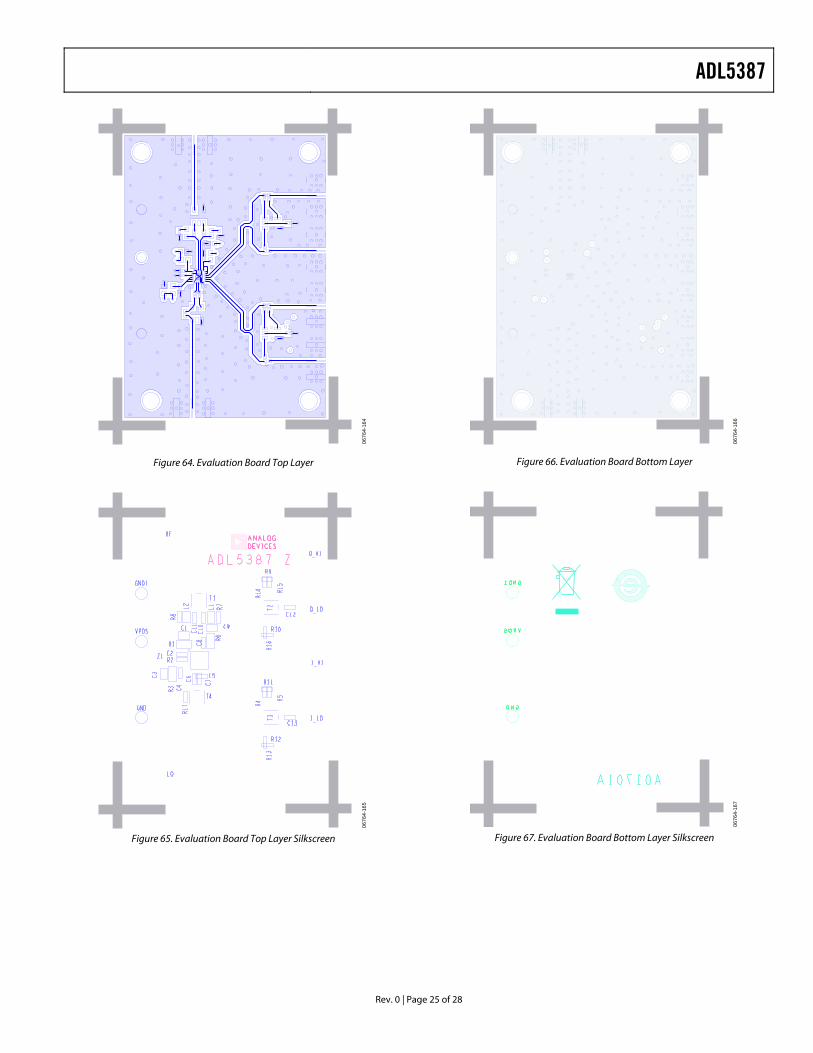
Rev. 0 | Page 25 of 28
0676
4-16
4
Figure 64. Evaluation Board Top Layer
0676
4-16
5
Figure 65. Evaluation Board Top Layer Silkscreen
0676
4-16
6
Figure 66. Evaluation Board Bottom Layer
0676
4-16
7
Figure 67. Evaluation Board Bottom Layer Silkscreen
ADL5387
Rev. 0 | Page 26 of 28
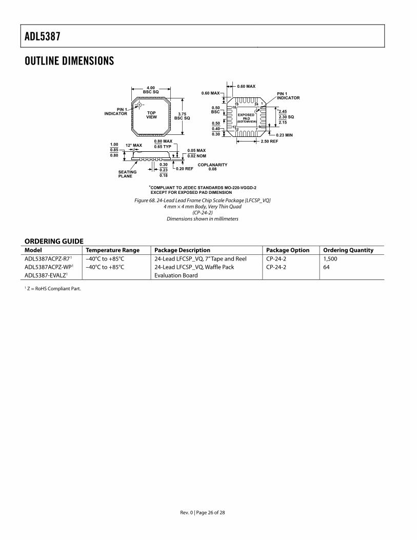
OUTLINE DIMENSIONS
*COMPLIANT TO JEDEC STANDARDS MO-220-VGGD-2EXCEPT FOR EXPOSED PAD DIMENSION
124
6713
1918
12
*2.452.30 SQ2.15
0.60 MAX
0.500.400.30
0.300.230.18
2.50 REF
0.50BSC
12° MAX0.80 MAX0.65 TYP
0.05 MAX0.02 NOM
1.000.850.80
SEATINGPLANE
PIN 1INDICATOR TOP
VIEW3.75
BSC SQ
4.00BSC SQ PIN 1
INDICATOR
0.60 MAX
COPLANARITY0.080.20 REF
0.23 MIN
EXPOSEDPAD
(BOTTOMVIEW)
Figure 68. 24-Lead Lead Frame Chip Scale Package [LFCSP_VQ]
4 mm × 4 mm Body, Very Thin Quad (CP-24-2)
Dimensions shown in millimeters
ORDERING GUIDE Model Temperature Range Package Description Package Option Ordering Quantity ADL5387ACPZ-R71 –40°C to +85°C 24-Lead LFCSP_VQ, 7” Tape and Reel CP-24-2 1,500 ADL5387ACPZ-WP1 –40°C to +85°C 24-Lead LFCSP_VQ, Waffle Pack CP-24-2 64 ADL5387-EVALZ1 Evaluation Board 1 Z = RoHS Compliant Part.

ADL5387
Rev. 0 | Page 27 of 28
NOTES

ADL5387
Rev. 0 | Page 28 of 28
NOTES
©2007 Analog Devices, Inc. All rights reserved. Trademarks and registered trademarks are the property of their respective owners. D06764-0-10/07(0)