500ma, ultra-low noise, high psrr cmos ldo regulator with ... · 500ma, ultra-low noise, high psrr...
TRANSCRIPT

LD6922 5/7/2011
1
Leadtrend Technology Corporation www.leadtrend.com.tw
LD6922-DS-02 May 2012
500mA, Ultra-Low Noise, High PSRR CMOS LDO Regulator
with Soft Start Function
REV: 02
General Description
The LD6922 is a micro power linear regulator with
minimum output voltage drop during load transient,
featuring ultra-low noise, low-dropout and high ripple
rejection ratio for optimal performance of battery-powered
systems. This SS pin can suppress the noise and is built in
with soft start function. As well, the LD6922 is stable with
an output capacitor of 1F which reduces the board space
and cost.
The LD6922 is available in a space saving SC82-4,
SOT23-5, SC70-5, SC70-6, and WDFN-6L 1.6mm x
1.6mm package.
+Patented
Features
Wide Operating Input Voltage Range:2.5V to 5.5V
Minimum Output Voltage Drop during Load Transient
Ultra-Low Noise for RF Application
Shutdown Current <1A
High PSRR 70dB@1kHz
Stable with 1F Output Capacitor
Thermal Shutdown and Current Limiting Protection
VOUT Discharge Function
Soft Start Operation
Fixed Output Voltage: 1.2V to 3.3V (step:0.1V), and
3.45V.
Applications
Battery-Powered Equipment
Hand-Held Instruments
Palmtops, Notebook Computers
Typical Application
VIN
CE
SS GND
OUT
LD6922
22nF/X7R
(option)
1μF
VIN VOUT
Enable1μF
*
Fig. 1 Typical Application Circuit for General Purpose

LD6922
2
Leadtrend Technology Corporation www.leadtrend.com.tw
LD6922-DS-02 May 2012
Pin Configuration
V : LD6922
Y : Year code (D: 2004, E: 2005…..)
W : Week code
X : voltage code (note 1)
VIN GND CE
OUT SS
SC70-6
1 2 3
4 6
VYWX
5
NC
SC82-4
CE GND
OUT VIN
4
1 2
3
VYWX
VIN GND CE
OUT SS
SC70-5
1 2 3
4 5
VYWX
WD F N-6 L (1.6m m x 1.6mm)
CE
GN
D
VI
N
SS
OU
T
NC
1 2 3
6 5 4
VXX
YWT
V : LD6922
XX: v o l t a g e c o d e (n o t e 2 )
XX : 345: 3.45V
T: T h i c k n e s s
W : 0 . 7 5 m m ( n o r m a l )
1 2 3
4 5
V I N G N D CE
O U T SS
Y WJ 22
XX
SOT-25
Y : Y e a r c o d e
W : W e e k c o d e
J22: LD6922
XX : v o l t a g e c o d e (n o t e 2 )
*Note 1 : Voltage Code for SC70-6, SC70-5, SC82-4
Code E F G H I J K L M N O P Q R S T U V W X
(V) 1.2 1.3 1.4 1.5 1.6 1.7 1.8 1.9 2.0 2.1 2.2 2.3 2.4 2.5 2.6 2.7 2.8 2.9 3.0 3.1
Code Y Z 5
(V) 3.2 3.3 3.45
*Note 2 : Voltage Code for SOT-25, WDFN-6L
Code 12 13 14 15 16 17 18 19 20 21 22 23 24 25 26 27 28 29 30 31
(V) 1.2 1.3 1.4 1.5 1.6 1.7 1.8 1.9 2.0 2.1 2.2 2.3 2.4 2.5 2.6 2.7 2.8 2.9 3.0 3.1
Code 32 33 345
(V) 3.2 3.3 3.45
Ordering Information
Part number Package TOP MARK Shipping
LD6922 GF-XX SC82-4 VYWX 3000 /tape & reel
LD6922 GL-XX SOT25 YWJ/22XX 3000 /tape & reel
LD6922 GC- XX SC70-5 VYWX 3000 /tape & reel
LD6922 GU- XX SC70-6 VYWX 3000 /tape & reel
LD6922 GDAW- XX WDFN-6L 1.6mm×1.6mm VXX 2500 /tape & reel
Note 1: The LD6922 is Green Packaged.
Note 2: Part number XX : Output voltage, ex: 12:1.2V…. 33:3.3V (step 0.1V) and 3.45V

LD6922
3
Leadtrend Technology Corporation www.leadtrend.com.tw
LD6922-DS-02 May 2012
Pin Descriptions
SC82-4
PIN NAME FUNCTION
1 CE Chip Enable, High=Enable, Low=Disable
2 GND IC GND
3 OUT Regulator output
4 VIN Input Voltage
SOT23-5, SC70-5
PIN NAME FUNCTION
1 VIN Input Voltage
2 GND IC GND
3 CE Chip Enable, High=Enable, Low=Disable
4 SS This pin combines noise reduction and soft start function. Connect a capacitor to
GND to adjust soft start time.
5 OUT Regulator output
SC70-6
PIN NAME FUNCTION
1 VIN Input Voltage
2 GND IC GND
3 CE Chip Enable, High=Enable, Low=Disable
4 SS This pin combines noise reduction and soft start function. Connect a capacitor to
GND to adjust soft start time.
5 NC No connection
6 OUT Regulator output
WDFN-6L
PIN NAME FUNCTION
1 CE Chip Enable, High=Enable, Low=Disable
2 GND IC GND
3 VIN Input Voltage
4 OUT Regulator output
5 NC No connection
6 SS This pin combines noise reduction and soft start function. Connect a capacitor to
GND to adjust soft start time.

LD6922
4
Leadtrend Technology Corporation www.leadtrend.com.tw
LD6922-DS-02 May 2012
Block Diagram (SC70-6)
CE
SS
OUT
Chip
Enable
Current Limit
&Thermal
Shutdown
Soft Start
VIN
VREF
R1
R2
200kΩ
GND
NC
Absolute Maximum Ratings
VIN, VOUT Pin -0.3V~6V
SS, CE Pin -0.3V~ (VIN+0.3) V
Power dissipation SC82-4@Ta=25C 300mW
Package Thermal Resistance SC82-4 333C/W
Power dissipation SOT23-5@Ta=25C 400mW
Package Thermal Resistance SOT25 250C/W
Power dissipation SC70-5@Ta=25C 300mW
Package Thermal Resistance SC70-5 333C/W
Power dissipation SC70-6@Ta=25C 300mW
Package Thermal Resistance SC70-6 333C/W
Power dissipation WDFN-6L 1.6×1.6 @TA=25C 571mW
Package Thermal Resistance WDFN-6L 1.6×1.6 175C/W
Maximum Junction Temperature 150C
Operating Junction Temperature -40C to 125C
Operating Ambient Temperature -40C to 85C
Storage Temperature Range -55C to 125C
Lead temperature (Soldering, 10sec) 260C
ESD Level (Human Body Model) 2kV
ESD Level (Machine Model) 200V
Caution:
Stresses beyond the ratings specified in “Absolute Maximum Ratings” may cause permanent damage to the device. This is a stress only
rating and operation of the device at these or any other conditions above those indicated in the operational sections of this specification
is not implied.

LD6922
5
Leadtrend Technology Corporation www.leadtrend.com.tw
LD6922-DS-02 May 2012
Electrical Characteristics
(VIN=VOUT+1V, TA = 25 C, unless otherwise stated. CIN=COUT=1μF, CSS=22nF; the LD6922 is tested with 3.1V output,
unless other stated.) (Note 1)
PARAMETER CONDITIONS MIN TYP MAX UNITS
INPUT POWER
Input Voltage 2.5 - 5.5 V
Quiescent Current CE>1.5V, IOUT=0mA - 80 105 A
Shutdown Supply Current CE=GND - 0.1 1 A
Dropt Voltage
Dropt Voltage (Note2) IOUT=300mA, 2.5VVIN3.6V 390 430 mV
IOUT=300mA, 3.6VVIN5.5V 230 300 mV
IOUT=500mA, 3.6VVIN5.5V 380 500 mV
Soft Start
Internal Soft Start Time 60 100 140 S
Output
Output Current Limit RLOAD=1 550 600 mA
Line Regulation VIN=VOUT +1V, to 5.5V,
IOUT=1mA - 0.05 0.2 %/V
Load Regulation
1mA<IOUT<300mA
VIN=VOUT+1V, 2.5VVOUT3.3V - 0.8 %
1mA<IOUT<500mA
VIN=VOUT+1V, 2.5VVOUT3.3V 1.6 %
Ripple Rejection
F=120Hz, EIN=1Vrms,
IOUT=10mA 70 dB
F=1kHz, EIN=1Vrms,
IOUT=10mA
70 - dB
F=10kHz, EIN=1Vrms,
IOUT=10mA
- 65 - dB
Output Noise Voltage VOUT=1.8V, IOUT=0mA
CSS=22nF - 35 - Vrms

LD6922
6
Leadtrend Technology Corporation www.leadtrend.com.tw
LD6922-DS-02 May 2012
PARAMETER CONDITIONS MIN TYP MAX UNITS
Discharge Resistance in
shutdown CE=High to Low - 80 160
CE
Impedance to GND 200 k
CE Input Level Enable, VIN=2.5V~5.5V 1.5 - - V
Disable, VIN=2.5V~5.5V - - 0.6 V
THERMAL PROTECTION
Thermal Shutdown VOUT short to GND 150 C
Hysteresis 30 C
Note1: Limits are 100% tested at TA =+25C. Limits over operating range are guarantee by design.
Note2: the drop voltage is defined as VIN-VOUT, which is measured when VOUT is VOUT (normal)-100mV.
Typical Performance Characteristics
(VIN=VOUT+1V, CIN=1F, COUT=1F, CSS=22nF, TA =+25C, unless otherwise stated.)
Rip
ple
Reje
ctio
n (
dB
)
Frequency (kHz) 0.01 0.1 1 10 100
Fig.3 Ripple Rejection vs. Frequency
20
30
40
50
60
70
80
Fig.4 Start Up Waveform Css=22nF
VCE
VIN
VOUT
CH1:2V/Div
CH2:2V/Div
CH3:2V/Div
10ms/Div
Fig.5 EN Pin Shutdown Response
VCE CH1: 2V/Div
VOUT CH3: 2V/Div
VIN CH2: 2V/Div
400s/Div
Fig.6 Output Noise (CSS=22nF)
VO CH2: 100Vrms/Div
VIN=4.3V
LD6922GL-345

LD6922
7
Leadtrend Technology Corporation www.leadtrend.com.tw
LD6922-DS-02 May 2012
Fig.7 Load Transient Response (CO=1F)
IO CH4: 100mA/Div
VO CH2: 10mV~/Div
20s/ Div
Typical Performance Characteristics
(VIN=VOUT+1V, CIN=4.7F, COUT=4.7F, CSS=22nF, TA =+25C, unless otherwise stated.)
Rip
ple
Reje
ctio
n (
dB
)
Frequency (kHz)
0.01 0.1 1 10 100
Fig.8 Ripple Rejection vs. Frequency
20
30
40
50
60
70
80
Fig.9 Start Up Waveform Css=22nF
VCE
VIN
VOUT
CH1:2V/Div
CH2:2V/Div
CH3:2V/Div 10ms/Div
Fig.10 EN Pin Shutdown Response
VCE CH1: 2V/Div
VOUT CH3: 2V/Div
VIN CH2: 2V/Div
400s/Div
Fig.11 Output Noise (CSS=22nF)
VO CH2: 100Vrms/Div
VIN=4.3V
LD6922GL-345

LD6922
8
Leadtrend Technology Corporation www.leadtrend.com.tw
LD6922-DS-02 May 2012
Fig.12 Load Transient Response (CO=4.7F)
IO CH4: 100mA/Div
VO CH2: 10mV/Div
20s/Div
Application Information
Operation Overview
It’s necessary to place an input capacitor of minimum
value 1F between VIN and GND to stabilize. It’s also
recommended to locate it in the distance of 5mm from
VIN.
The output capacitor is also recommended to place in the
distance of 5mm from OUT pin. The LD6922 performs
well in cooperating with low ESR ceramic output capacitor,
ideally for compact applications. To enhance the stability,
the ceramic capacitor of 1μF at least and larger ESR than
25m
always best suited for full range of operation temperature.
Soft Start Operation and Noise Reduction
If an external soft start capacitor, CSS, is used between SS
and GND, it will provide soft start operation and reduce
output noise efficiently. We can obtain the soft start time
according to the following formula.
Where,
TSS: soft start time (ms)
CSS: soft start capacitor (nF)
EX:
VOUT=3.1V and CSS=22nF
The soft start time, TSS ≈ 0.93 x 22= 20.46 (ms)
The LD6922 is also built with internal soft start of
60~140S, it’s eliminable for an external soft start
capacitor.
Enable Function
The LD6922 features enable/ disable function. The CE pin
will completely turn on the device once it receives input of
logic high level over 1.5V. On the other hand, the device
will enter shutdown mode when the voltage drops below
0.6V. In shutdown mode, it consumes current less than
1A (max).
Current Limit
Output current is limited to 600mA (typical). When current
limit engages, the output voltage scales back linearly until
the over-current condition ends. Take care not to exceed
the power dispassion ratings of the package.
Thermal Consideration
When the junction temperature exceeds Tj=150C, the
thermal sensor will turn off the pass transistor and cool
down the IC. The thermal sensor turns on the pass
transistor after the IC’s junction temperature falls by 30C

LD6922
9
Leadtrend Technology Corporation www.leadtrend.com.tw
LD6922-DS-02 May 2012
(typical). For continuous operation, do not exceed
absolute maximum operation junction temperature of
125C. The maximum power dissipation is determined
according to following equation.
JA
A)MAX(J)MAX(D
)TT(P
JA: Package Thermal Resistance
The maximum power dispassion at Ta=25C can be obtained by above formula.
PDMAX=(125C-25C)/250=400mW
…………….……….( SOT23-5 package)
PDMAX=(125C-25C)/333=300mW
…………….……….( SC82-4 package)
PDMAX=(125C-25C)/333=300mW
……………………..( SC70-5, SC70-6 package)
PDMAX=(125C-25C)/175=571mW
……………………..(WDFN-6L 1.6x1.6 package)

LD6922
10
Leadtrend Technology Corporation www.leadtrend.com.tw
LD6922-DS-02 May 2012
Package Information
SC82-4
Symbol Dimension in Millimeters Dimensions in Inches
Min Max Min Max
A 1.800 2.200 0.071 0.087
B 1.150 1.350 0.045 0.053
C 0.800 1.100 0.031 0.043
D 0.250 0.400 0.010 0.016
D1 0.350 0.500 0.014 0.020
E 1.300 TYP. 0.051 TYP.
H 0.100 0.260 0.004 0.010
I 0.000 0.100 0.000 0.004
J 1.800 2.400 0.071 0.094
M 0.260 0.460 0.010 0.018
θ 0° 8° 0° 8°

LD6922
11
Leadtrend Technology Corporation www.leadtrend.com.tw
LD6922-DS-02 May 2012
SOT-25
Symbol Dimension in Millimeters Dimensions in Inches
Min Max Min Max
A 2.692 3.099 0.106 0.122
B 1.397 1.803 0.055 0.071
C --- 1.450 --- 0.057
D 0.300 0.500 0.012 0.020
E 1.90 TYP 0.074 TYP
F 0.95 TYP 0.037 TYP
H 0.080 0.254 0.003 0.010
I 0.050 0.150 0.002 0.006
J 2.600 3.000 0.102 0.118
M 0.300 0.600 0.012 0.024
θ 0° 10° 0° 10°
LD6922
12
Leadtrend Technology Corporation www.leadtrend.com.tw
LD6922-DS-02 May 2012
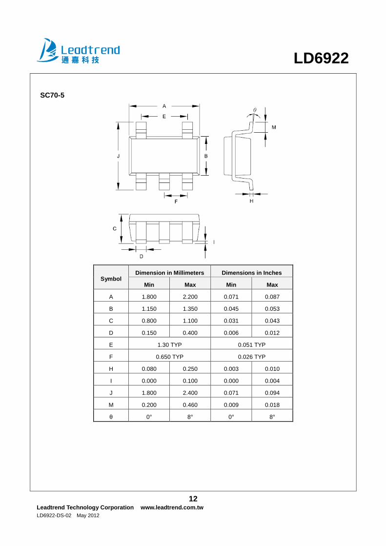
SC70-5
Symbol Dimension in Millimeters Dimensions in Inches
Min Max Min Max
A 1.800 2.200 0.071 0.087
B 1.150 1.350 0.045 0.053
C 0.800 1.100 0.031 0.043
D 0.150 0.400 0.006 0.012
E 1.30 TYP 0.051 TYP
F 0.650 TYP 0.026 TYP
H 0.080 0.250 0.003 0.010
I 0.000 0.100 0.000 0.004
J 1.800 2.400 0.071 0.094
M 0.200 0.460 0.009 0.018
θ 0° 8° 0° 8°
LD6922
13
Leadtrend Technology Corporation www.leadtrend.com.tw
LD6922-DS-02 May 2012
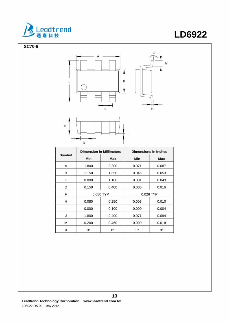
SC70-6
Symbol Dimension in Millimeters Dimensions in Inches
Min Max Min Max
A 1.800 2.200 0.071 0.087
B 1.150 1.350 0.045 0.053
C 0.800 1.100 0.031 0.043
D 0.150 0.400 0.006 0.016
F 0.650 TYP 0.026 TYP
H 0.080 0.250 0.003 0.010
I 0.000 0.100 0.000 0.004
J 1.800 2.400 0.071 0.094
M 0.200 0.460 0.009 0.018
θ 0° 8° 0° 8°

LD6922
14
Leadtrend Technology Corporation www.leadtrend.com.tw
LD6922-DS-02 May 2012
WDFN-6L (1.6mm 1.6 mm)
DETAIL X
THE CONFIGURATION OF THE PIN 1
IDENTIFIER IS OPTIONAL AS ABOVE.
Symbol Dimensions in Millimeters Dimensions in Inches
Min. Max. Min. Max.
A 1.500 1.700 0.059 0.067
B 1.500 1.700 0.059 0.067
C 0.700 0.800 0.028 0.031
D 0.200 0.300 0.008 0.012
E 0.900 1.100 0.035 0.043
F 0.500 TYP. 0.019 TYP.
G 0.203 TYP. 0.008 TYP.
H 0.500 0.700 0.020 0.028
I 0.000 0.050 0.000 0.002
M 0.200 0.300 0.009 0.012

LD6922
15
Leadtrend Technology Corporation www.leadtrend.com.tw
LD6922-DS-02 May 2012
IR Profile for SMD Devices
0
50
100
150
200
250
300
Temp.
(ºc)
Time (sec.)
Ramp up
3ºC/second
max.
217ºC
60 ~ 150 seconds
Peak Temp.
260 -5/+0ºC, 30 seconds
(max.)
Preheat
60 ~ 120 seconds
260
217
Ramp down
6ºC/second max.
Item Average
Ramp-up Rate
Pre-heat
(150 ~ 200°C)
Time Maintained
Above 217°C Peak Temp.
Ramp-down
Rate
Required 3°C(max)
/sec 60~120 sec 60~150 seconds
260 +0/-5°C
30 seconds
6°C (max)
/sec
Important Notice
Leadtrend Technology Corp. reserves the right to make changes or corrections to its products at any time without notice.
Customers should verify the datasheets are current and complete before placing order.
LD6922
16
Leadtrend Technology Corporation www.leadtrend.com.tw
LD6922-DS-02 May 2012
Revision History
Rev. Date Change Notice
00 08/03/2011 Original Specification
01 09/01/2011 Package Option: SC70-5
02 5/7/2012 Dropt voltage description