6-bit flash adc for high speed applications.pdf · and-hold (t/h) circuit, a comparator array...
TRANSCRIPT
International Journal of Science and Research (IJSR) ISSN (Online): 2319-7064
Impact Factor (2012): 3.358
Volume 3 Issue 10, October 2014 www.ijsr.net
Licensed Under Creative Commons Attribution CC BY
6-Bit Flash ADC for High speed Applications
N. Bharat Kumar Reddy1, Sri D. Sharath Babu Rao2
1Student of M.Tech in VLSI & EMBEDDED Systems, Electronics and Communication Engineering, GPREC (Autonomous), KURNOOL,
JNTU-A, Andhra Pradesh, India
2Assistant Professor of Electronics and Communication Engineering, GPREC (Autonomous), KURNOOL, JNTU-A, Andhra Pradesh, India
Abstract: This paper shows the implementation of a 6-bit Flash Analog to Digital Converter in 130-nm technology CMOS logic functions at 2.5-GSamples/s, used in most of DSP-based receiver. The FLSH ADC is equipped by variable gain amplifier (VGA), track-and-hold (T/H) circuit, a comparator array consist of 63 comparators, D Flip-Flop’s. A multiplexer logic is compared with the decoder using Full Adders in Wallace tree structure, with respect to hardware, critical path and power consumption. The Multiplexer logic is used to convert the 63-Bit Thermometer code into 6-Bit Binary code. Also integrated a on chip micro controller calibration, is used to monitor and compensate the nominal nonlinearity of the fine VGA and the resistor ladder. The ADC with 400mV of full scale voltage consumes 15-30 m W of power approximately from a 0.9V supply. Keywords: 10G Ethernet, Digitally programmable resistor array, A/D conversion, Metastability errors, Wallace tree decoder; Multiplexer based decoder, Short critical path.
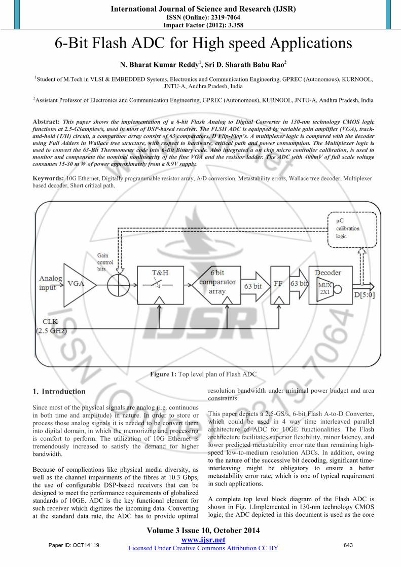
Figure 1: Top level plan of Flash ADC
1. Introduction Since most of the physical signals are analog (i.e. continuous in both time and amplitude) in nature. In order to store or process those analog signals it is needed to be convert them into digital domain, in which the memorizing and processing is comfort to perform. The utilization of 10G Ethernet is tremendously increased to satisfy the demand for higher bandwidth. Because of complications like physical media diversity, as well as the channel impairments of the fibres at 10.3 Gbps, the use of configurable DSP-based receivers that can be designed to meet the performance requirements of globalized standards of 10GE. ADC is the key functional element for such receiver which digitizes the incoming data. Converting at the standard data rate, the ADC has to provide optimal
resolution bandwidth under minimal power budget and area constraints. This paper depicts a 2.5-GS/s, 6-bit Flash A-to-D Converter, which could be used in 4 way time interleaved parallel architecture of ADC for 10GE functionalities. The Flash architecture facilitates superior flexibility, minor latency, and lower predicted metastability error rate than remaining high-speed low-to-medium resolution ADCs. In addition, owing to the nature of the successive bit decoding, significant time-interleaving might be obligatory to ensure a better metastability error rate, which is one of typical requirement in such applications. A complete top level block diagram of the Flash ADC is shown in Fig. 1.Implemented in 130-nm technology CMOS logic, the ADC depicted in this document is used as the core
Paper ID: OCT14119 643
International Journal of Science and Research (IJSR) ISSN (Online): 2319-7064
Impact Factor (2012): 3.358
Volume 3 Issue 10, October 2014 www.ijsr.net
Licensed Under Creative Commons Attribution CC BY
for the 4 way interleaved analog frontend runs at 10GSamples/s for a DSP-based receiver that can be used the NRZ 10GE standards. While this paper focuses on the design and implementation of decoder for the ADC, and on comparative analysis of decoder implementation using Wallace tree adder and Multiplexer. 2. ADC Architecture The on-chip micro Computer first calibrates the ADC upon receiver start-up, and then continuously compensates the non-linearities in VGA and inter-channel mismatch during the normal operation of the ADC. The ADC consists of a frontend Variable Gain Amplifier (G) which provides fine control of gain. Each instance of G drives a Track and Hold (T/H) circuitry that is clocked by a 2.5-GHz clock. The comparator array of 63 comparators is fed by the sampled analog signal and reference signals which are generated by a resister ladder network with 400m V of full-scale voltage. To prevent Metastability-related error propagation, the thermometer code goes through a sequence of flip-flops before arriving at the decoder inputs. Together with the comparator and the SR latch, this guarantees metastability error rate betterment. A multiplexer logic then converts the Metastability-hardened thermometer code into binary. Finally, the output is retimed to a single clock phase. 3. Circuit Implementation 3.1 Variable Gain Amplifier
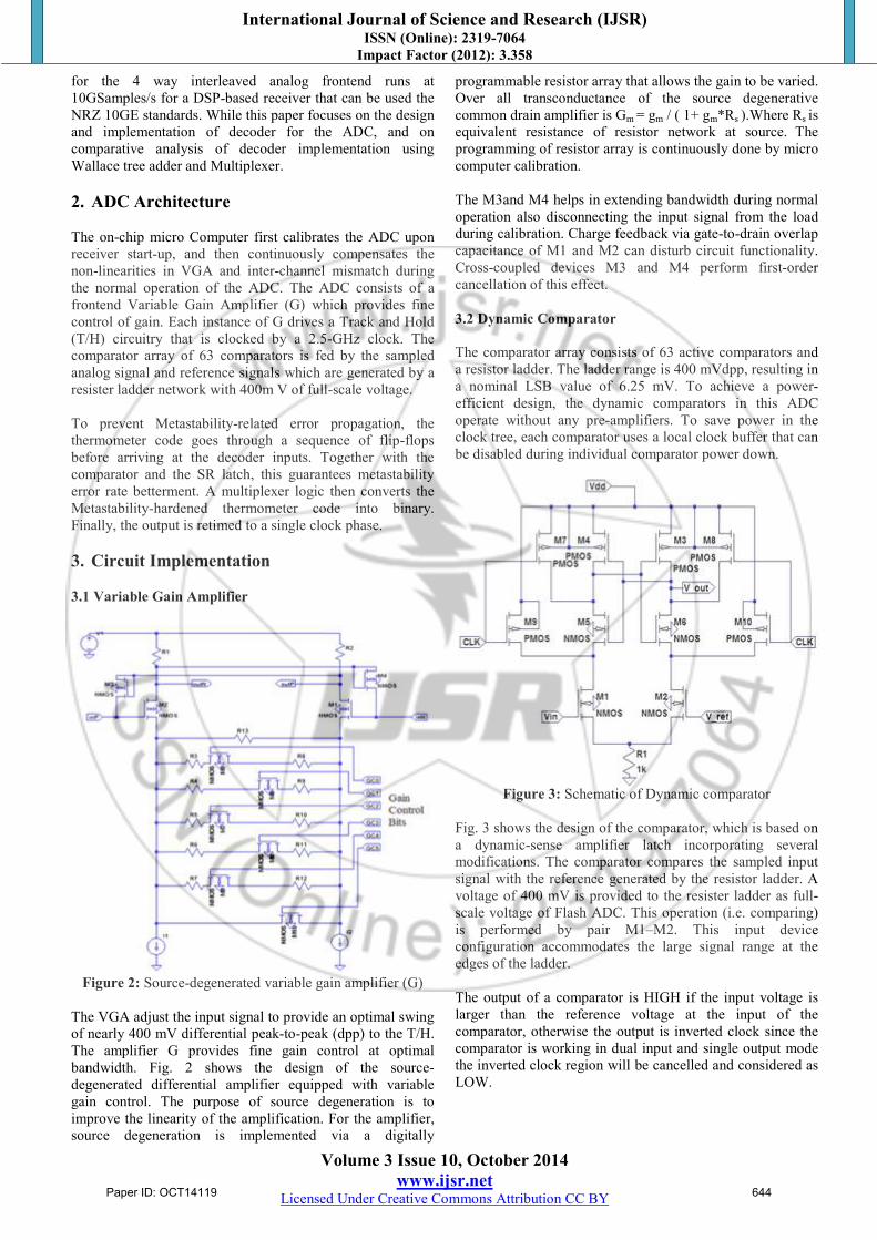
Figure 2: Source-degenerated variable gain amplifier (G)
The VGA adjust the input signal to provide an optimal swing of nearly 400 mV differential peak-to-peak (dpp) to the T/H. The amplifier G provides fine gain control at optimal bandwidth. Fig. 2 shows the design of the source-degenerated differential amplifier equipped with variable gain control. The purpose of source degeneration is to improve the linearity of the amplification. For the amplifier, source degeneration is implemented via a digitally
programmable resistor array that allows the gain to be varied. Over all transconductance of the source degenerative common drain amplifier is Gm = gm / ( 1+ gm*Rs ).Where Rs is equivalent resistance of resistor network at source. The programming of resistor array is continuously done by micro computer calibration. The M3and M4 helps in extending bandwidth during normal operation also disconnecting the input signal from the load during calibration. Charge feedback via gate-to-drain overlap capacitance of M1 and M2 can disturb circuit functionality. Cross-coupled devices M3 and M4 perform first-order cancellation of this effect. 3.2 Dynamic Comparator The comparator array consists of 63 active comparators and a resistor ladder. The ladder range is 400 mVdpp, resulting in a nominal LSB value of 6.25 mV. To achieve a power-efficient design, the dynamic comparators in this ADC operate without any pre-amplifiers. To save power in the clock tree, each comparator uses a local clock buffer that can be disabled during individual comparator power down.
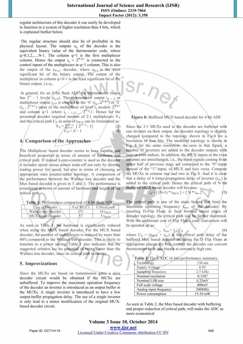
Figure 3: Schematic of Dynamic comparator
Fig. 3 shows the design of the comparator, which is based on a dynamic-sense amplifier latch incorporating several modifications. The comparator compares the sampled input signal with the reference generated by the resistor ladder. A voltage of 400 mV is provided to the resister ladder as full-scale voltage of Flash ADC. This operation (i.e. comparing) is performed by pair M1–M2. This input device configuration accommodates the large signal range at the edges of the ladder. The output of a comparator is HIGH if the input voltage is larger than the reference voltage at the input of the comparator, otherwise the output is inverted clock since the comparator is working in dual input and single output mode the inverted clock region will be cancelled and considered as LOW.
Paper ID: OCT14119 644

International Journal of Science and Research (IJSR)
Licensed Under Creative Commons Attribution CC BY
3.3 Decoders 3.3.1. The Wallace tree decoder The output of a thermometer-to-binarysummation of digital ones on the input, representedgray or binary code. This will be chosen counter as a decoder and gives the similarswapping technique.
Figure 4: Wallace tree decoder for a 4 However, the bit swapping techniquethermometer decoder, since the output rectified thermometer code. Using theoutput is the decoded binary code and it alsobubble error suppression. One more approach of using the ones-counter as decoderon the speed constraint on the ADC a suitabletopology may be selected by a speed for powerhigh-speed applications the Wallace treein Fig. 4.
Figure 5: Realization of Full Adder using A full adder can be constructed from threewith two multiplexers in the critical path fig. 5.The reason behind this realizationcomparative study of Wallace tree decoderdecoder. Hence, for N bit decoder, themultiplexers needed (YN) and the criticalWallace tree decoder are formulated as:
YN = 3*[ ∑ �� � 1����� .
CN = 2*[2N – 3] for N >CN = 2*[N] for N = 1 The units of CN is equal to the propagationXOR gate ( tXOR ) which is similar to the propagationof a 2:1 multiplexer (tMUX ).
International Journal of Science and Research (IJSR)ISSN (Online): 2319-7064
Impact Factor (2012): 3.358
Volume 3 Issue 10, October 2014 www.ijsr.net
Licensed Under Creative Commons Attribution CC BY
binary decoder is the represented in, e.g., when using a ones
similar result as the bit
4-bit flash ADC
technique also needed a is a bubble error
the ones-counter the also performs global advantage of the
decoder is that based suitable ones-counter power trade-off. For
tree topology is shown
using 2:1 Multiplexers
three 2:1 multiplexers as described in the
realization is to simplify the decoder with MUX based
the number of 2:1 critical path (CN) for the
� . 2(N- i)] (1) > 1 (2)
propagation delay of a 2-input propagation delay
3.3.2 The Multiplexer Based This subdivision will first illustratepresented multiplexer based how it could be generalized. most significant bit (MSB) ofmore than half of the outputslogic one. Hence is the same as1 level. To find the value of the(MSB-1) the original thermometerpartial thermometer scales, separatedlevel as depicted as the flow diagram
Figure 6: Implementation of 4
Figure 7: Flow of Multipl The partial thermometer scale 2:1 multiplexers, where the earlierfed as the control input of thedetermined from the chosen partialidentical fashion as was foundscale. The selected scale is therebyinformation about MSB-1, i.e.scale if the output at level is logicpartial thermometer scale is used. This conversion is continued multiplexer remains. Its output(LSB) of the binary output. Theby the 4-bit multiplexer based
International Journal of Science and Research (IJSR)
decoder illustrate the idea behind the decoder and second describe For an N-bit flash ADC the
of the binary output is high if outputs in the thermometer scale are
as the thermometer output at 2N-
the second most significant bit thermometer scale is bifurcated into
separated by the output at 2N-1 diagram in Fig. 6.
4 bit Multiplexer based decoder
Multiplexer based decoding
to decode is chosen by a set of earlier decoded binary output is the multiplexers.MSB-1 is then partial thermometer scale in the
found from the full thermometer thereby the scale that includes the i.e. the lower partial thermometer
logic zero otherwise the upper used.
recursively until only one 2:1 output is the least significant bit
The decoder scheme is illustrated based decoder in Fig. 5. Due to the
Paper ID: OCT14119 645
International Journal of Science and Research (IJSR)
Licensed Under Creative Commons Attribution CC BY
regular architecture of this decoder it can to function in a system of higher resolutionis explained further below. The regular structure should also be ofphysical layout. The outputs xq of theequivalent binary value of the thermometerq=0,1,2,.....N-1. The column q=1 is thecolumn. Hence the output iq = 2N-q-1 iscontrol inputs of the multiplexers in q+1 column.the output of the xN-q-1 decoder, wheresignificant bit of the binary output. Themultiplexer in column q=N-1 is the least significantbinary output, i.e.x0. In general, for an N-bit flash ADC the thermometerhas 2N - 1 levels (iq=0). The thermometermultiplexer output iq>0 is coupled to the ‘0’(iq < 2N-q-1) input of the multiplexer of leveland column q+1 ,where iq = 1,2,3,...... 2N-
presented decoder required number of 2:1and the critical path CN in units of tMUX can
YN = ∑ ���� ��� 2(N- i)
-CN = N – 1
4. Comparison of the Approaches The Multiplexer based decoder seems tobeneficial properties in terms of amountcritical path. If instead a ones-counter is usedit includes speed versus power trade-off nottrading power for speed, but also in termsappropriate ones counter/adder topology.the performance between the Wallace treeMux based decoder is given in T able 1. considered in terms of amount of hardwarecritical path.
Table 1: Performance comparison of 6Type of Decoder N.of MUX’s
Wallace tree Decoder 171 MUX based Decoder 57
As seen in Table 1, the hardware is significantlywhen using the MUX based decoder. Fordecoder, the number of multiplexers is reduced60% compared to the Wallace tree decoder.translate to a power saving. Table 1 alsosuggested solution has the potential of beingWallace tree decoder, since its critical path 5. Improvizations Since the MUXs are based on transmissiondecoder circuit would be obtained ifunbuffered. To improve the maximum operationof the decoder an inverter is introduced asthe MUXs. A single inverter is introducedoutput-buffer propagation delay. The use is only lead to a minor modification of based decoder circuit.
International Journal of Science and Research (IJSR)ISSN (Online): 2319-7064
Impact Factor (2012): 3.358
Volume 3 Issue 10, October 2014 www.ijsr.net
Licensed Under Creative Commons Attribution CC BY
easily be developed resolution than 4 bits, which
of profitable in the the decoder is the
thermometer code, where the first multiplexer is connected to the column. This is also
where xN-1 is the most The output of the significant bit of the
thermometer output thermometer output iq = 0 or
‘0’ (iq < 2N-q-1) or ‘1’ level iq modulo 2N-q-1
-q-1. Hence for the 2:1 multiplexers YN
can be formulated as: - 1] (3)
(4)
Approaches
to have capable and amount of hardware and
used as the decoder not only by directly
terms of choosing an topology. A comparison of
tree decoder and the The performance is
hardware and length of the
6 bit flash ADC MUX’s Critical path
18 tMUX 5 tMUX
significantly reduced For the MUX based
reduced by more than decoder. This is likely to
also indicates that the being faster than the
path is shorter.
transmission gates a slow if the MUXs are operation frequency
as an output buffer in introduced to have a low
of a single inverter the original MUX-
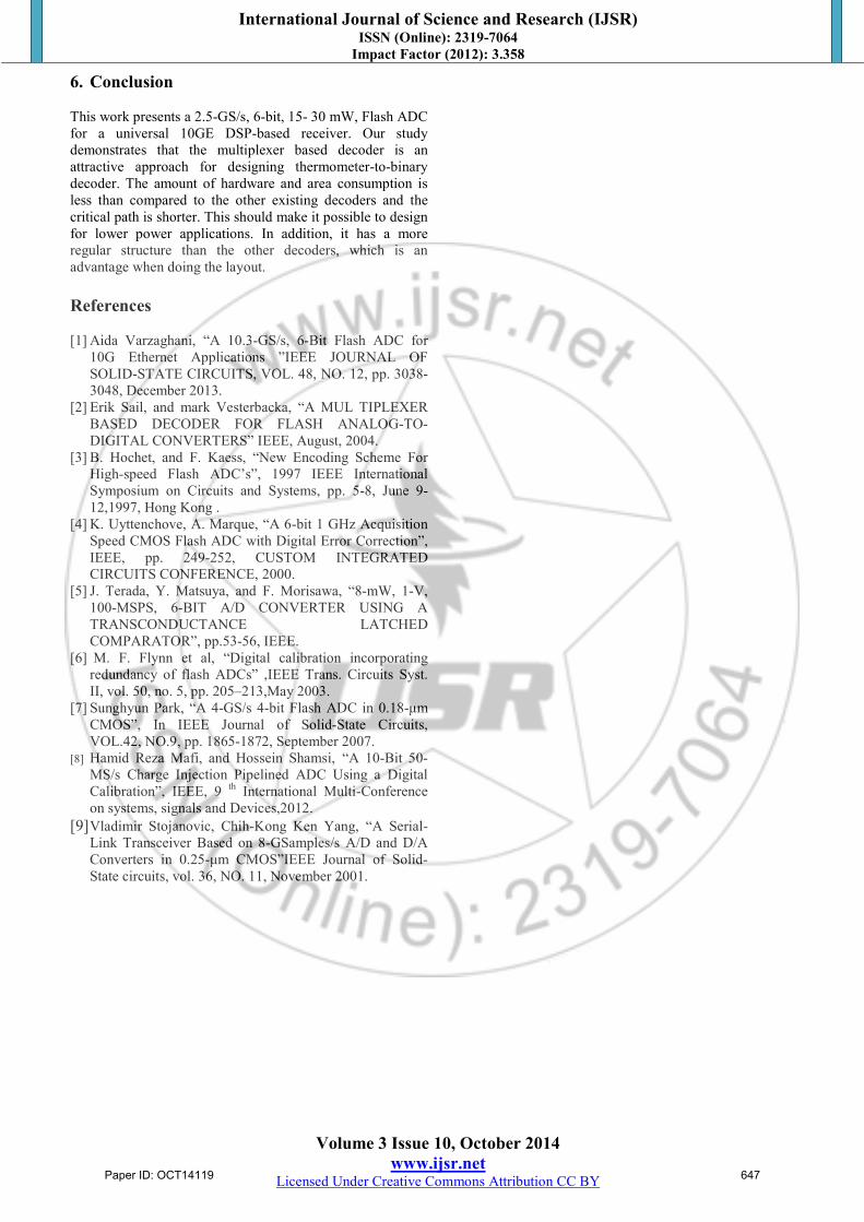
Figure 8: Buffered MUX based Since the 2:1 MUXs used in one inverter on their output, thechanged compared to the topologyresolution of four bits. The modifiedFig. 8 for the same resolution.number of inverters are addedzero or even indices. In addition,columns are interchanged, i.e.,upper half of previous stage areinstead of the “1”-input, of MUXthe MUXs in column one andthat a delay of 4 times propagationadded to the critical path. HenceBuffered MUX based decoder
CN = [ (N-1) * tMUX The critical path is one of themaximum operating frequencyinserting D-Flip Flops in feeddecoder topology, the critical With the additional cost of Flipbe speeded up as:
fmax = 1 where CN = (tMUX + tinv) is buffered Mux based decoder appropriate places. By this conceptthermometer code into binary at
Table 2: Flash ADC (6 bit)Technology Supply Voltage Sampling frequency Nominal resolution Nominal LSB size Full scale voltage Analog input frequency Power consumption
As seen in Table 2, the Mux basedand proper reduction of criticalmore economical
International Journal of Science and Research (IJSR)
based decoder for 4 bit ADC
the decoder are buffered with the decoder topology is slightly
topology shown in Fig.6 for a modified topology is shown in
resolution. As seen in that figure, a added to the decoder outputs with
addition, the MUX inputs in the even i.e., the input signals coming from
are connected to the “0”-input MUX and vice versa. Compare
and two in Fig 8. And it is clear propagation delay of inverter (tinv) is
Hence the critical path of N bit will become:
MUX ] + [ N * tinv ] (5)
the main factors that limit the frequency fmax of the decoder. By
feed forward cutest edges of path will be further shortened.
Flip Flops, code conversion will
/ CN (6) the critical path delay of the including the D Flip Flops at
concept the decoder can convert at extremely high rate.
bit) performance summary. 130 nm
0.9V 2.5 GHz 0.1587
6.25mV 400mV
200MHz 15-30 mW
based decoder with buffering critical path, will make the ADC as
Paper ID: OCT14119 646
International Journal of Science and Research (IJSR) ISSN (Online): 2319-7064
Impact Factor (2012): 3.358
Volume 3 Issue 10, October 2014 www.ijsr.net
Licensed Under Creative Commons Attribution CC BY
6. Conclusion This work presents a 2.5-GS/s, 6-bit, 15- 30 mW, Flash ADC for a universal 10GE DSP-based receiver. Our study demonstrates that the multiplexer based decoder is an attractive approach for designing thermometer-to-binary decoder. The amount of hardware and area consumption is less than compared to the other existing decoders and the critical path is shorter. This should make it possible to design for lower power applications. In addition, it has a more regular structure than the other decoders, which is an advantage when doing the layout. References
[1] Aida Varzaghani, “A 10.3-GS/s, 6-Bit Flash ADC for
10G Ethernet Applications ”IEEE JOURNAL OF SOLID-STATE CIRCUITS, VOL. 48, NO. 12, pp. 3038-3048, December 2013.
[2] Erik Sail, and mark Vesterbacka, “A MUL TIPLEXER BASED DECODER FOR FLASH ANALOG-TO-DIGITAL CONVERTERS” IEEE, August, 2004.
[3] B. Hochet, and F. Kaess, “New Encoding Scheme For High-speed Flash ADC’s”, 1997 IEEE International Symposium on Circuits and Systems, pp. 5-8, June 9-12,1997, Hong Kong .
[4] K. Uyttenchove, A. Marque, “A 6-bit 1 GHz Acquisition Speed CMOS Flash ADC with Digital Error Correction”, IEEE, pp. 249-252, CUSTOM INTEGRATED CIRCUITS CONFERENCE, 2000.
[5] J. Terada, Y. Matsuya, and F. Morisawa, “8-mW, 1-V, 100-MSPS, 6-BIT A/D CONVERTER USING A TRANSCONDUCTANCE LATCHED COMPARATOR”, pp.53-56, IEEE.
[6] M. F. Flynn et al, “Digital calibration incorporating redundancy of flash ADCs” ,IEEE Trans. Circuits Syst. II, vol. 50, no. 5, pp. 205–213,May 2003.
[7] Sunghyun Park, “A 4-GS/s 4-bit Flash ADC in 0.18-μm CMOS”, In IEEE Journal of Solid-State Circuits, VOL.42, NO.9, pp. 1865-1872, September 2007.
[8] Hamid Reza Mafi, and Hossein Shamsi, “A 10-Bit 50-MS/s Charge Injection Pipelined ADC Using a Digital Calibration”, IEEE, 9 th International Multi-Conference on systems, signals and Devices,2012.
[9] Vladimir Stojanovic, Chih-Kong Ken Yang, “A Serial-Link Transceiver Based on 8-GSamples/s A/D and D/A Converters in 0.25-μm CMOS”IEEE Journal of Solid-State circuits, vol. 36, NO. 11, November 2001.
Paper ID: OCT14119 647