contentsweb.stanford.edu/group/cioffi/doc/book/chap6.pdfchapter 6 fundamentals of synchronization...
TRANSCRIPT
Contents
6 Fundamentals of Synchronization 5266.1 Phase computation and regeneration . . . . . . . . . . . . . . . . . . . . . . . . . . . . . . 528
6.1.1 Phase Error Generation . . . . . . . . . . . . . . . . . . . . . . . . . . . . . . . . . 5286.1.2 Voltage Controlled Oscillators . . . . . . . . . . . . . . . . . . . . . . . . . . . . . . 5306.1.3 Maximum-Likelihood Phase Estimation . . . . . . . . . . . . . . . . . . . . . . . . 532
6.2 Analysis of Phase Locking . . . . . . . . . . . . . . . . . . . . . . . . . . . . . . . . . . . . 5336.2.1 Continuous Time . . . . . . . . . . . . . . . . . . . . . . . . . . . . . . . . . . . . . 5336.2.2 Discrete Time . . . . . . . . . . . . . . . . . . . . . . . . . . . . . . . . . . . . . . . 5356.2.3 Phase-locking at rational multiples of the provided frequency . . . . . . . . . . . . 539
6.3 Symbol Timing Synchronization . . . . . . . . . . . . . . . . . . . . . . . . . . . . . . . . . 5416.3.1 Open-Loop Timing Recovery . . . . . . . . . . . . . . . . . . . . . . . . . . . . . . 5416.3.2 Decision-Directed Timing Recovery . . . . . . . . . . . . . . . . . . . . . . . . . . . 5436.3.3 Pilot Timing Recovery . . . . . . . . . . . . . . . . . . . . . . . . . . . . . . . . . . 545
6.4 Carrier Recovery . . . . . . . . . . . . . . . . . . . . . . . . . . . . . . . . . . . . . . . . . 5466.4.1 Open-Loop Carrier Recovery . . . . . . . . . . . . . . . . . . . . . . . . . . . . . . 5466.4.2 Decision-Directed Carrier Recovery . . . . . . . . . . . . . . . . . . . . . . . . . . . 5476.4.3 Pilot Carrier Recovery . . . . . . . . . . . . . . . . . . . . . . . . . . . . . . . . . . 548
6.5 Frame Synchronization in Data Transmission . . . . . . . . . . . . . . . . . . . . . . . . . 5496.5.1 Autocorrelation Methods . . . . . . . . . . . . . . . . . . . . . . . . . . . . . . . . 5496.5.2 Searcing for the guard period or pilots . . . . . . . . . . . . . . . . . . . . . . . . . 551
6.6 Pointers and Add/Delete Methods . . . . . . . . . . . . . . . . . . . . . . . . . . . . . . . 552Exercises - Chapter 6 . . . . . . . . . . . . . . . . . . . . . . . . . . . . . . . . . . . . . . . . . 554
525

Chapter 6
Fundamentals of Synchronization
The analysis and developments of Chapters 1-4 presumed that the modulator and demodulator aresynchronized. That is, both modulator and demodulator know the exact symbol rate and the exactsymbol phase, and where appropriate, both also know the exact carrier frequency and phase. In practice,the common (receiver/transmitter) knowledge of the same timing and carrier clocks rarely occurs unlesssome means is provided for the receiver to synchronize with the transmitter. Such synchronization isoften called phase-locking.
In general, phase locking uses three component operations as generically depicted in Figure 6.1:1
1. Phase-error generation - this operation, sometimes also called “phase detection,” derives aphase difference between the received signal’s phase θ(t) and the receiver estimate of this phase,θ(t). The actual signals are s(t) = cos (ωlot + θ(t)) and s(t) = cos
(ωlot + θ(t)
), but only their
phase difference is of interest in synchronization. This difference is often called the phase error,φ(t) = θ(t) − θ(t). Various methods of phase-error generation are discussed in Section 6.1.
2. Phase-error processing - this operation, sometimes also called “loop filtering” extracts theessential phase difference trends from the phase error by averaging. Phase-error processing typicallyrejects random noise and other undesirable components of the phase error signal. Any gain in thephase detector is assumed to be absorbed into the loop filter. Both analog and digital phase-errorprocessing, and the general operation of what is known as a “phase-lock loop,” are discussed inSection 6.2.
3. Local phase reconstruction - this operation, which in some implementations is known as a“voltage-controlled oscillator” (VCO), regenerates the local phase from the processed phase errorin an attempt to match the incoming phase, θ(t). That is, the phase reconstruction tries to forceφ(t) = 0 by generation of a local phase θ(t) so that s(t) matches s(t). Various types of voltagecontrolled oscillators and other methods of regenerating local clock are also discussed in Section6.1
Any phase-locking mechanism will have some finite delay in practice so that the regenerated localphase will try to project the incoming phase and then measure how well that projection did in theform of a new phase error. The more quickly the phase-lock mechanism tracks deviations in phase, themore susceptible it will be to random noise and other imperfections. Thus, the communication engineermust trade these two competing effects appropriately when designing a synchronization system. Thedesign of the transmitted signals can facilitate or complicate this trade-off. These design trade-offswill be generally examined in Section 6.2. In practice, unless pilot or control signals are embedded inthe transmitted signal, it is necessary either to generate an estimate of transmitted signal’s clocks or togenerate an estimate of the phase error directly. Sections 6.3 and 6.4 specifically examine phase detectorsfor situations where such clock extraction is necessary for timing recovery (recovery of the symbol clock)and carrier recovery (recovery of the phase of the carrier in passband transmission), respectively. In
1These operations may implemented in a wide variety of ways.
526

Figure 6.1: General phase-lock loop structure.
addition to symbol timing, data is often packetized or framed. Methods for recovering frame boundaryare discussed in Section 6.5. Pointers and add/delete (bit robbing/stuffing) are specific mechanisms oflocal phase reconstruction that allow the use of asynchronous clocks in the transmitter and receiver.These methods find increasing use in modern VLSI implementations of receivers and are discussed inSection 6.6.
527

Figure 6.2: Comparison of ideal and mod-2π phase detectors.
6.1 Phase computation and regeneration
This section describes the basic operation of the phase detector and of the voltage-controlled oscillator(VCO) in Figure 6.1 in more detail.
6.1.1 Phase Error Generation
Phase-error generation can be implemented continuously or at specific sampling instants. The discussionin this subsection will therefore not use a time argument or sampling index on phase signals. That isθ(t) → θ.
Ideally, the two phase angles, θ, the phase of the input sinusoid s, and θ, the estimated phase producedat the VCO output, would be available. Then, their difference φ could be computed directly.
Definition 6.1.1 (ideal phase detector) A device that can compute exactly the differenceφ = θ − θ is called an ideal phase detector.
Ideally, the receiver would have access to the sinusoids s = cos(θlo + θ) and s = cos(θlo + θ) where θlo
is the common phase reference that depends on the local oscillator frequency; θlo disappears from theensuing arguments, but in practice the general frequency range of dθ
dt = ωlo will affect implementations.A seemingly straightforward method to compute the phase error would then be to compute θ, the phaseof the input sinusoid s, and θ, the estimated phase, according to
θ = ± arccos [s] − θlo ; θ = ± arccos [s] − θlo . (6.1)
Then, φ = θ−θ, to which the value θlo is inconsequential in theory. However, a reasonable implementationof the arccos function can only produce angles between 0 and π, so that φ would then always lie between−π and π. Any difference of magnitude greater than π would be thus effectively be computed modulo(−π, π). The arccos function could then be implemented with a look-up table.
Definition 6.1.2 (mod-2π phase detector) The arccos look-up table implementation ofthe phase detector is called a modulo-2π phase detector2.
The characteristics of the mod-2π phase detector and the ideal phase detector are compared in Figure6.2. If the phase difference does exceed π in magnitude, the large difference will not be exhibited in thephase error φ - this phenomenon is known as a “cycle slip,” meaning that the phase lock loop missed (oradded) an entire period (or periods) of the input sinusoid. This is an undesirable phenomena in most
2Sometimes also called a “sawtooth” phase detector after the phase characteristic in Figure 6.2.
528

Figure 6.3: Demodulating phase detector.
Figure 6.4: Sampling phase detector.
applications, so after a phase-lock loop with mod-2π phase detector has converged, one tries to ensurethat |φ| cannot exceed π. In practice, a good phase lock loop should keep this phase error as close tozero as possible, so the condition of small phase error necessary for use of the mod-2π phase detectoris met. The means for avoiding cycle slips is to ensure that the local-oscillator frequency is less thandouble the desired frequency and greater than 1/2 that same local-oscillator frequency.
Definition 6.1.3 (demodulating phase detector) Another commonly encountered phasedetector, both in analog and digital form, is the demodulating phase detector shown inFigure 6.3, where
φ = f ∗[− sin(θlo + θ) · cos(θlo + θ)
], (6.2)
and f is a lowpass filter that is cascaded with the phase-error processing in the phase-lockingmechanism.
The basic concept arises from the relation
− cos (ωlot + θ) · sin(ωlot + θ
)=
12
{− sin
(2ωlot + θ + θ
)+ sin
(θ − θ
)}, (6.3)
where the sum-phase term (first term on the right) can be eliminated by lowpass filtering; this lowpassfiltering can be absorbed into the loop filter that follows the phase detector (see Section 6.2). The phasedetector output is thus proportional to sin (φ). The usual assumption with this type of phase detectoris that φ is small (φ << π
6 ), and thussin (φ) ≈ φ . (6.4)
When φ is small, generation of the phase error thus does not require the arcsin function.Another way of generating the phase error signal is to use the local sinusoid to sample the incoming
529
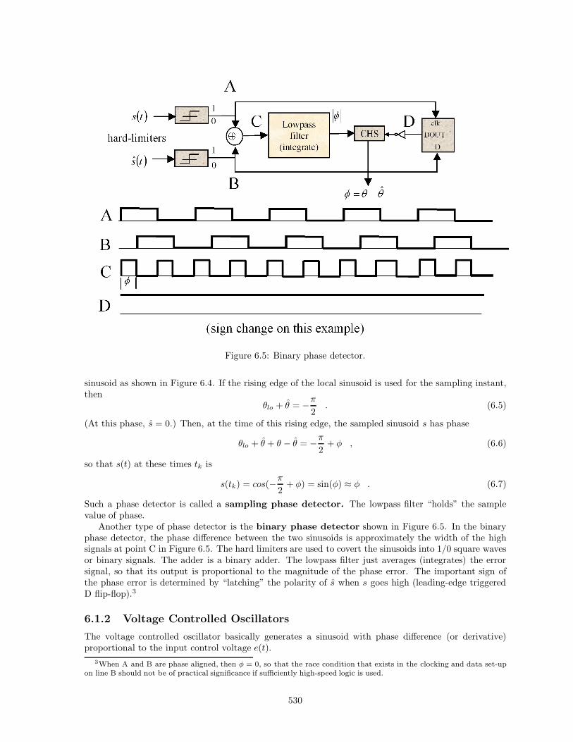
Figure 6.5: Binary phase detector.
sinusoid as shown in Figure 6.4. If the rising edge of the local sinusoid is used for the sampling instant,then
θlo + θ = −π
2. (6.5)
(At this phase, s = 0.) Then, at the time of this rising edge, the sampled sinusoid s has phase
θlo + θ + θ − θ = −π
2+ φ , (6.6)
so that s(t) at these times tk is
s(tk) = cos(−π
2+ φ) = sin(φ) ≈ φ . (6.7)
Such a phase detector is called a sampling phase detector. The lowpass filter “holds” the samplevalue of phase.
Another type of phase detector is the binary phase detector shown in Figure 6.5. In the binaryphase detector, the phase difference between the two sinusoids is approximately the width of the highsignals at point C in Figure 6.5. The hard limiters are used to covert the sinusoids into 1/0 square wavesor binary signals. The adder is a binary adder. The lowpass filter just averages (integrates) the errorsignal, so that its output is proportional to the magnitude of the phase error. The important sign ofthe phase error is determined by “latching” the polarity of s when s goes high (leading-edge triggeredD flip-flop).3
6.1.2 Voltage Controlled Oscillators
The voltage controlled oscillator basically generates a sinusoid with phase difference (or derivative)proportional to the input control voltage e(t).
3When A and B are phase aligned, then φ = 0, so that the race condition that exists in the clocking and data set-upon line B should not be of practical significance if sufficiently high-speed logic is used.
530

Figure 6.6: Discrete-time VCO with all-digital realization.
Definition 6.1.4 (Voltage Controlled Oscillator) An ideal voltage controlled oscil-lator (VCO) has an output sinusoid with phase θ(t) that is determined by an input erroror control signal according to
dθ
dt= kvco · e(t) , (6.8)
in continuous time, or approximated by
θk+1 = θk + kvco · ek . (6.9)
in discrete time.
Analog VCO physics are beyond the scope of this text, so it will suffice to just state that devices satisfying(6.8) are readily available in a variety of frequency ranges. When the input signal ek in discrete timeis digital, the VCO can also be implemented with a look-up table and adder according to (6.9) whoseoutput is used to generate a continuous time sinusoidal equivalent with a DAC. This implementation isoften called a numerically controlled oscillator or NCO.
Yet another implementation that can be implemented in digital logic on an integrated circuit isshown in Figure 6.6. The high-rate clock is divided by the value of the control signal (derived from ek)by connecting the true output of the comparator to the clear input of a counter. The higher the clockrate with respect to the rates of interest, the finer the resolution on specifying θk. If the clock rate is1/T ′, then the divider value is p or p+1, depending upon whether the desired clock phase is late or early,respectively. A maximum phase change with respect to a desired phase (without external smoothing)can thus be T ′/2. For 1% clock accuracy, then the master clock would need to be 50 times the generatedclock frequency. With an external analog smoothing of the clock signal (via bandpass filter centeredaround the nominal clock frequency), a lower frequency master clock can be used. Any inaccuracy inthe high-rate clock is multiplied by p so that the local oscillator frequency must now lay in the intervalflo ·
((1 − 1
2p ), flo · (1 + p))
to avoid cycle slipping. (When p = 1, this reduces to the interval mentionedearlier.) See also Section 6.2.3 on phase-locking at rational multiples of a clock frequency.
The Voltage-Controlled Crystal Oscillator (VCXO)
In many situations, the approximate clock frequency to be derived is known accurately. Conventionalcrystal oscillators usually have accuracies of 50 parts per million (ppm) or better. Thus, the VCO needonly track over a small frequency/phase range. Additionally in practice, the derived clock may be usedto sample a signal with an analog-to-digital converter (ADC). Such an ADC clock should not jitterabout its nominal value (or significant signal distortion can be incurred). In this case, a VCXO normally
531

replaces the VCO. The VCXO employs a crystal (X) of nominal frequency to stabilize the VCO closeto the nominal value. Abrupt changes in phase are not possible because of the presence of the crystal.However, the high stability and slow variation of the clock can be of crucial importance in digital receiverdesigns. Thus, VCXO’s are used instead of VCO’s in designs where high stability sample clocking isnecessary.
Basic Jitter effect
The effect of oscillator jitter is approximated for a waveform x(t) according to
δx ≈ dx
dtδt , (6.10)
so that
(δx)2 ≈(
dx
dt
)2
(δt)2 . (6.11)
A signal-to-jitter-noise ratio can be defined by
SNR =x2
(δx)2=
x2
(dx/dt)2(δt)2. (6.12)
For the highest frequency component of x(t) with frequency fmax, the SNR becomes
SNR =1
4π2(fmax · δt)2, (6.13)
which illustrates a basic time/frequency uncertainty principle: If (δt)2 represents jitter in squared sec-onds, then jitter must become smaller as the spectrum of the signal increases. An SNR of 20 dB (factorof 100 in jitter) with a signal with maximum frequency of 1 MHz would suggest that jitter be below 16ns.
6.1.3 Maximum-Likelihood Phase Estimation
A number of detailed developments on phase lock loops attempt to estimate phase from a likelihoodfunction:
maxx,θ
py/x,θ . (6.14)
Maximization of such a function can be complicated mathematically, often leading to a series of approx-imations for various trigonometric functions that ultimately lead to a quantity proportional to the phaseerror that is then used in a phase-lock loop. Such approaches are acknowledged here, but those interestedin the ultimate limits of synchronization performance are referred elsewhere. Practical approximationsunder the category of “decision-directed” synchronization methods in Sections 6.3.2 and 6.4.2.
532

Figure 6.7: Continuous-time PLL with loop filter.
6.2 Analysis of Phase Locking
Both continuous-time and discrete-time PLL’s are analyzed in this section. In both cases, the loop-filter characteristic is specified for both first-order and second-order PLL’s. First-order loops are foundto track only constant phase offsets, while second-order loops can track both phase and/or frequencyoffsets.
6.2.1 Continuous Time
The continuous-time PLL has a phase estimate that follows the differential equation
˙θ(t) = kvco · f(t) ∗
(θ(t) − θ(t)
). (6.15)
The transfer function between PLL output phase and input phase is
θ(s)θ(s)
=kvco · F (s)
s + kvco · F (s)(6.16)
with s the Laplace transform variable. The corresponding transfer function between phase error andinput phase is
φ(s)θ(s)
= 1 − θ(s)θ(s)
=s
s + kvco · F (s). (6.17)
The cases of both first- and second-order PLL’s are shown in Figure 6.7 with β = 0, reducing thediagram to a first-order loop.
First-Order PLL
The first order PLL haskvco · F (s) = α (6.18)
533

(a constant) so that phase errors are simply integrated by the VCO in an attempt to set the phase θ suchthat φ = 0. When φ =0, there is zero input to the VCO and the VCO output is a sinusoid at frequencyωlo. Convergence to zero phase error will only happen when s(t) and s(t) have the same frequency (ωlo)with initially a constant phase difference that can be driven to zero under the operation of the first-orderPLL, as is subsequently shown.
The response of the first-order PLL to an initial phase offset (θ0) with
θ(s) =θ0
s(6.19)
isθ(s) =
α · θ0
s(s + α)(6.20)
orθ(t) =
(θ0 − θ0 · e−αt
)· u(t) (6.21)
where u(t) is the unit step function (=1, for t > 0, = 0 for t < 0). For stability, α > 0. Clearly
θ(∞) = θ0 . (6.22)
An easier analysis of the PLL final value is through the final value theorem:
φ(∞) = lims→0
s · φ(s) (6.23)
= lims→0
s · θ0
s + α(6.24)
= 0 , (6.25)
so that the final phase error is zero for a unit-step phase input. For a linearly varying phase (that is aconstant frequency offset), θ(t) = (θ0 + ∆t)u(t), or
θ(s) =θ0
s+
∆s2
, (6.26)
where ∆ is the frequency offset
∆ =dθ
dt− ωlo . (6.27)
In this case, the final value theorem illustrates the first-order PLL’s eventual phase error is
φ(∞) =∆α
. (6.28)
A larger “loop gain” α causes a smaller the offset, but a first-order PLL cannot drive the phase errorto zero. The steady-state phase instead lags the correct phase by ∆/α. However, larger α forces largerthe bandwidth of the PLL. Any small noise in the phase error then will pass through the loop withless attenuation by the PLL, leading to a more noisy phase estimate. As long as |∆/α| < π, then themodulo-2π phase detector functions with constant non-zero phase error. The range of ∆ for which thephase error does not exceed π is known as the pull range of the PLL
pull range = |∆| < |α| · π . (6.29)
That is, any frequency deviation less than the pull range will result in a constant phase “lag” error.Such a non-zero phase error may or may not present a problem for the associated transmission system.A better method by which to track frequency offset is the second-order PLL.
534

Figure 6.8: Discrete-time PLL.
Second-Order PLL
The second order PLL uses the loop filter to integrate the incoming phase errors as well as pass theerrors to the VCO. The integration of errors eventually supplies a constant signal to the VCO, which inturn forces the VCO output phase to vary linearly with time. That is, the frequency of the VCO canthen be shifted away from ωlo permanently, unlike the operation with first-order PLL.
In the second-order PLL,
kvco ·F (s) = α +β
s. (6.30)
Thenθ(s)θ(s)
=αs + β
s2 + αs + β, (6.31)
andφ(s)θ(s)
=s2
s2 + αs + β. (6.32)
One easily verifies with the final value theorem that for either constant phase or frequency offset (orboth) that
φ(∞) = 0 (6.33)
for the second-order PLL. For stability,
α > 0 (6.34)β > 0 . (6.35)
6.2.2 Discrete Time
This subsection examines discrete-time first-order and second-order phase-lock loops. Figure 6.8 is thediscrete-time equivalent of Figure 6.1. Again, the first-order PLL only recovers phase and not frequency.The second-order PLL recovers both phase and frequency. The discrete-time VCO follows
θk+1 = θk + kvco · fk ∗ φk , (6.36)
535

and generates cos(ωlo · kT + θk
)as the local phase at sampling time k. This expression assumes discrete
“jumps” in the phase of the VCO. In practice, such transitions will be smoothed by any VCO thatproduces a sinusoidal output and the analysis here is only approximate for kT ≤ t ≤ (k + 1)T , where Tis the sampling period of the discrete-time PLL. Taking the D-Transforms of both sides of (6.36) equatesto
D−1 · Θ(D) = [1 − kvco · F (D)] · Θ(D) + kvco ·F (D) · Θ(D) . (6.37)
The transfer function from input phase to output phase is
Θ(D)Θ(D)
=D · kvco · F (D)
1 − (1 − kvco · F (D)) D. (6.38)
The transfer function between the error signal Φ(D) and the input phase is thus
Φ(D)Θ(D)
=Θ(D)Θ(D)
− Θ(D)Θ(D)
= 1 − D · kvco ·F (D)1 − (1 − kvco · F (D)) D
=D − 1
D(1 − kvco · F (D)) − 1. (6.39)
F (D) determines whether the PLL is first- or second-order.
First-Order Phase Lock Loop
In the first-order PLL, the loop filter is a (frequency-independent) gain α, so that
kvco · F (D) = α . (6.40)
ThenΘ(D)Θ(D)
=αD
1 − (1 − α)D. (6.41)
For stability, |1 − α| < 1, or0 ≤ α < 2 (6.42)
for stability. The closer α to 2, the wider the bandwidth of the overall filter from Θ(D) to Θ(D), and themore (any) noise in the input sinusoid can distort the estimated phase. The first-order loop can trackand drive to zero any phase difference between a constant θk and θk. To see this effect, the input phaseis
θk = θ0 ∀ k ≥ 0 , (6.43)
which has D-TransformΘ(D) =
θ0
1 − D. (6.44)
The phase-error sequence then has transform
Φ(D) =D − 1
D (1 − kvcoF (D)) − 1Θ(D) (6.45)
=(D − 1)θ0
(1 − D)(D(1 − α) − 1)(6.46)
=θ0
1 − (1 − α)D(6.47)
Thus
φk ={
θ0(1 − α)k k ≥ 00 k < 0 , (6.48)
and φ∞ → 0 if (6.42) is satisfied. This result can also be obtained by the final value theorem for one-sidedD-Transforms
limk→∞ φk = lim
D→1 (1 − D) · Φ(D) = 0 . (6.49)
536

The first-order loop will exhibit a constant phase offset, at best, for any frequency deviation betweenθk and θk. To see this constant-lag effect, the input phase can be set to
θk = ∆ · k ∀ k ≥ 0 , (6.50)
where ∆ = ωoffsetT , which has D-Transform4
Θ(D) =∆D
(1 − D)2. (6.51)
The phase-error sequence then has transform
Φ(D) =D − 1
D (1 − kvco ·F (D)) − 1Θ(D) (6.52)
=D − 1
D (1 − kvco ·F (D)) − 1· ∆D
(1 − D)2(6.53)
=∆D
(1 − D)(1 − D(1 − α))(6.54)
This steady-state phase error can also be computed by the final value theorem
limk→∞ φk = lim
D→1 (1 − D)Φ(D) =∆α
. (6.55)
This constant-lag phase error is analogous to the same effect in the continuous-time PLL. Equation(6.55) can be interpreted in several ways. The main result is that the first order loop cannot track anonzero frequency offset ∆ = ωoffsetT , in that the phase error cannot be driven to zero. For very smallfrequency offsets, say a few parts per million of the sampling frequency or less, the first-order loop willincur only a very small penalty in terms of residual phase error (for reasonable α satisfying (6.42)). Inthis case, the first-order loop may be sufficient in terms of magnitude of phase error, in nearly estimatingthe frequency offset. In order to stay within the linear range of the modulo-2π phase detector (therebyavoiding cycle slips) after the loop has converged, the magnitude of the frequency offset |ωoffset| mustbe less than απ
T . The reader is cautioned not to misinterpret this result by inserting the maximum α(=2) into this result and concluding than any frequency offset can be tracked with a first-order loop aslong as the sampling rate is sufficiently high. Increasing the sampling rate 1/T at fixed α, or equivalentlyincreasing α at fixed sampling rate, increase the bandwidth of the phase-lock loop filter. Any noise onthe incoming phase will be thus less filtered or “less rejected” by the loop, resulting in a lower qualityestimate of the phase. A better solution is to often increase the order of the loop filter, resulting in thefollowing second-order phase lock loop.
As an example, let us consider a PLL attempting to track a 1 MHz clock with a local oscillatorclock that may deviate by as much as 100 ppm, or equivalently 100 Hz in frequency. The designer maydetermine that a phase error of π/20 is sufficient for good performance of the receiver. Then,
ωoffset · Tα
≤ π
20(6.56)
orα ≥ 40 · foffset · T . (6.57)
Then, since foffset = 100 Hz, and if the loop samples at the clock speed of 1/T = 106 MHz, then
α > 4 × 10⁻³ . (6.58)
Such a small value of α is within the stability bound of 0 < α < 2. If the phase error or phase estimateare relatively free of any “noise,” then this value is probably acceptable. However, if either the accuracyof the clock is less or the sampling rate is less, then an unacceptably large value of α can occur.
4Using the relation that (D) dFdD
↔ kxk , with xk = ∆ ∀ k ≥ 0.
537

Noise Analysis of the First-Order PLL If the phase input to the PLL (that is θk) has some zero-mean “noise” component with variance σ2
θ , then the component of the phase error caused by the noiseis
Φn(D) =1 − D
1 − [1− α] · D·Nθ(D) (6.59)
or equivalentlyφk = (1 − α) · φk−1 + nθ,k − nθ,k−1 . (6.60)
By squaring the above equation and finding the steady-state constant value σ2φ,k = σ2
φ,k−1 = σ2φ and
setting E [nθ,k · nθ,k−l] = σ2θ · δl via algebra,
σ2φ =
σ2θ
1 − α/2. (6.61)
Larger values of α create larger response to the input phase noise. If α → 2, the phase error variancebecomes infinite. Small values of α are thus attractive, limiting the ability to keep the constant phaseerror small. The solution is to use the second-order PLL of the next subsection.
Second-Order Phase Lock Loop
In the second-order PLL, the loop filter is an accumulator of phase errors, so that
kvco · F (D) = α +β
1 − D. (6.62)
This equation is perhaps better understood by rewriting it in terms of the second order differenceequations for the phase estimate
∆k = ∆k−1 + βφk (6.63)
θk+1 = θk + αφk + ∆k (6.64)
In other words, the PLL accumulates phase errors into a frequency offset (times T ) estimate ∆k, whichis then added to the first-order phase update at each iteration. Then
Θ(D)Θ(D)
=(α + β)D − αD2
1− (2 − α − β)D + (1 − α)D2, (6.65)
which has poles 1
(1−α+β2 )±
√( α+β
2 )2−β. For stability, α and β must satisfy,
0 ≤ α < 2 (6.66)
0 ≤ β < 1 − α
2−
√α2
2− 1.5α + 1 . (6.67)
Typically, β <(
α+β2
)2
for real roots, which makes β << α since α + β < 1 in most designs.
The second-order loop will track for any frequency deviation between θk and θk. To see this effect,the input phase is again set to
θk = ∆k ∀ k ≥ 0 , (6.68)
which has D-TransformΘ(D) =
∆D
(1 − D)2. (6.69)
The phase-error sequence then has transform
Φ(D) =D − 1
D (1 − kvco · F (D)) − 1Θ(D) (6.70)
=(1 − D)2
1 − (2 − α − β)D + (1 − α)D2· ∆D
(1 − D)2(6.71)
=∆D
1 − (2 − α − β)D + (1 − α)D2(6.72)
538

This steady-state phase error can also be by the final value theorem
limk→∞ φk = lim
D→1 (1 − D)Φ(D) = 0 . (6.73)
Thus, as long as the designer chooses α and β within the stability limits, a second-order loop should beable to track any constant phase or frequency offset. One, however, must be careful in choosing α andβ to reject noise, equivalently making the second-order loop too sharp or narrow in bandwidth, can alsomake its initial convergence to steady-state very slow. The trade-offs are left to the designer for anyparticular application.
Noise Analysis of the Second-Order PLL The power transfer function from any phase noisecomponent at the input to the second-order PLL to the output phase error is found to be:
| 1 − e−jmathω |4
| 1 − (2 − α − β)e−jmathω + (1 − α)e2ω |2. (6.74)
This transfer-function can be calculated and multiplied by any input phase-noise power spectral densityto get the phase noise at the output of the PLL. Various stable values for α and β (i.e., that satisfyEquations (6.66) and (6.67) ) may be evaluated in terms of noise at the output and tracking speed ofany phase or frequency offset changes. Such analysis becomes highly situation dependent.
Phase-Jitter Noise Specifically following the noise analysis, a phase noise may have a strong compo-nent at a specific frequency (which is often called “phase jitter.” Phase jitter often occurs at either thepower-line frequency (50-60 Hz) or twice the power line frequency (100-120 Hz) in many systems.5 Inother situations, other radio-frequency or ringing components can be generated by a variety of devicesoperating within the vicinity of the receiver. In such a situation, the choices of α and β may be suchas to try to cause a notch at the specific frequency. A higher-order loop filter might also be used tointroduce a specific notch, but overall loop stability should be checked as well as the transfer function.
6.2.3 Phase-locking at rational multiples of the provided frequency
Clock frequencies or phase errors may not always be computed at the frequency of interest. Figure 6.9illustrates the translation from a phase error measured at frequency 1
Tto a frequency p
q· 1
T= 1
T ′ wherep and q are any positive co-prime integers. The output frequency to be used from the PLL is 1/T ′. Ahigh frequency clock with period
T ′′ =T
p=
T ′
q(6.75)
is used so that
pT ′′ = T (6.76)qT ′′ = T ′ . (6.77)
The divides in Figure 6.9 use the counter circuits in Figure 6.6. To avoid cycle slips, the local oscillatorshould be between flo ·
((1 − p
2), (1 + p)
).
5This is because power supplies in the receiver may have a transformer from AC to DC internal voltages in chips orcomponents and it is difficult to completely eliminate leakage of the energy going through the transformer via parasiticpaths into other components.
539
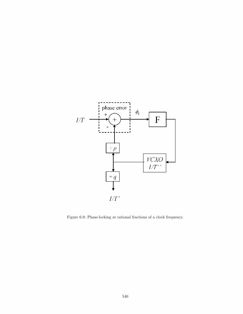
Figure 6.9: Phase-locking at rational fractions of a clock frequency.
540

Figure 6.10: Square-law timing recovery.
6.3 Symbol Timing Synchronization
Generally in data transmission, a sinusoid synchronized to the symbol rate is not supplied to the receiver.The receiver derives this sinusoid from the received data. Thus, the unabetted PLL’s studied so far wouldnot be sufficient for recovering the symbol rate. The recovery of this symbol-rate sinusoid from thereceived channel signal, in combination with the PLL, is called timing recovery. There are two typesof timing recovery. The first type is called open loop timing recovery and does not use the receiver’sdecisions. The second type is called decision-directed or decision-aided and uses the receiver’sdecisions. Such metods are an approximation to the ML synchronization in (6.14). Since the recoveredsymbol rate is used to sample the incoming waveform in most systems, care must be exerted in thehigher-performance decision-directed methods that not too much delay appears between the samplingdevice and the decision device. Such delay can seriously degrade the performance of the receiver or evenrender the phase-lock loop unstable.
Subsection 6.3.1 begins with the simpler open-loop methods and Subsection 6.3.2 then progresses todecision-directed methods.
6.3.1 Open-Loop Timing Recovery
Probably the simplest and most widely used timing-recovery method is the square-law timing-recoverymethod of Figure 6.10. The present analysis ignores the optional prefilter momentarily, in which casethe nonlinear squaring device produces at its output
y2(t) =
[∑
m
xmp(t − mT ) + n(t)
]2
. (6.78)
The expected value of the square output (assuming, as usual, that the successively transmitted datasymbols xm are independent of one another) is
E{y2(t)
}=
∑
m
∑
n
Ex · δmn · p(t − mT ) · p(t − nT ) + σ2n (6.79)
= Ex ·∑
m
p2(t − mT ) + σ2n , (6.80)
which is periodic, with period T . The bandpass filter attempts to replace the statistical average in (6.80)by time-averaging. Equivalently, one can think of the output of the square device as the sum of its meanvalue and a zero-mean noise fluctuation about that mean,
y2(t) = E{y2(t)
}+
(y2(t) − E
{y2(t)
}). (6.81)
The second term can be thought of as noise as far as the recovery of the timing information from the firstterm. The bandpass filter tries to reduce this noise. The instantaneous values for this noise depend uponthe transmitted data pattern and can exhibit significant variation, leading to what is sometimes called“data-dependent” timing jitter. The bandpass filter and PLL try to minimize this jitter. Sometimes“line codes” (or basis functions) are designed to insure that the underlying transmitted data patternresults in significantly less data-dependent jitter effects. Line codes are seqential encoders (see Chapter
541

Figure 6.11: Envelope timing recovery.
Figure 6.12: Bandedge timing recovery.
8) that use the system state to amplify clock-components in any particular stream of data symbols.Well-designed systems typically do not need such codes, and they are thus not addressed in this text.
While the signal in (6.80) is periodic, its amplitude may be small or even zero, depending on p(t).This amplitude is essentially the value of the frequency-domain convolution P (f) ∗ P (f) evaluated atf = 1/T – when P (f) has small energy at f = 1/(2T ), then the output of this convolution typically hassmall energy at f = 1/T . In this case, other “even” nonlinear functions can replace the squaring circuit.Examples of even functions include a fourth-power circuit, and absolute value. Use of these functionsmay be harder to analyze, but basically their use attempts to provide the desired sinusoidal output. Theeffectiveness of any particular choice depends upon the channel pulse response. The prefilter can be usedto eliminate signal components that are not near 1/2T so as to reduce noise further. The PLL at the endof sqare-law timing recovery works best when the sinusoidal component of 1/2T at the prefilter outputhas maximum amplitude relative to noise amplitude. This maximum amplitude occurs for a specificsymbol-clock phase. The frequency 1/2T is the “bandedge”. Symbol-timing recovery systems often tryto select a timing phase (in addition to recovering the correct clock frequency) so that the bandedgecomponent is maximized. Square-law timing recovery by itself does not guarantee a maximum bandedgecomponent.
For QAM data transmission, the equivalent of the square-law timing recovery is known as envelopetiming recovery, and is illustrated in Figure 6.11. The analysis is basically the same as the realbaseband case, and the nonlinear element could be replaced by some other nonlinearity with real output,for instance the equivalent of absolute value would be the magnitude (square root of the sum of squaresof the two real and imaginary inputs). A problem with envelope timing is the a prior need for the carrier.
One widely used method for avoiding the carrier-frequency dependency is the so-called “bandedge”timing recovery in Figure 6.12. The two narrowband bandpass filters are identical. Recall from the earlier
542

discussion about the fractionally spaced equalizer in Chapter 3 that timing-phase errors could lead toaliased nulls within the Nyquist band. The correct choice of timing phase should lead (approximately)to a maximum of the energy within the two bandedges. This timing phase would also have maximizedthe energy into a square-law timing PLL. At this band-edge maximizing timing phase, the output of themultiplier following the two bandpass filters in Figure 6.12 should be maximum, meaning that quantityshould be real. The PLL forces this timing phase by using the samples of the imaginary part of themultiplier output as the error signal for the phase-lock loop. While the carrier frequency is presumedto be known in the design of the bandpass filters, knowledge of the exact frequency and phase is notnecessary in filter design and is otherwise absent in “bandedge” timing recovery.
6.3.2 Decision-Directed Timing Recovery
Decisions can also be used in timing recovery. A common decision-directed timing recovery methodminimizes the mean-square error, over the sampling time phase, between the equalizer (if any) outputand the decision, as in Figure 6.13. That is, the receiver chooses τ to minimize
J(τ ) = E{|xk − z(kT + τ )|2
}, (6.82)
where z(kT + τ ) is the equalizer output (LE or DFE ) at sampling time k corresponding to samplingphase τ . The update uses a stochastic-gradient estimate of τ in the opposite direction of the unaveragedderivative of J(τ ) with respect to τ . This derivative is (letting εk
∆= xk − z(kT + τ ))
dJ
dτ= <
[E
{2ε∗k · (−
dz
dτ)}]
. (6.83)
The (second-order) update is then
τk+1 = τk + α · <{ε∗k · z} + Tk (6.84)Tk = Tk−1 + β · <{ε∗k · z} . (6.85)
This type of decision-directed phase-lock loop is illustrated in Figure 6.13. There is one problem inthe implementation of the decision-directed loop that may not be obvious upon initial inspection ofFigure 6.13: the implementation of the differentiator. The problem of implementing the differentiatoris facilitated if the sampling rate of the system is significantly higher than the symbol rate. Then thedifferentiation can be approximated by simple differences between adjacent decision inputs. However, ahigher sampling rate can significantly increase system costs.
Another symbol-rate sampling approach is to assume that zk corresponds to a bandlimited waveformwithin the Nyquist band:
z(t + τ ) =∑
m
zm · sinc(t + τ − mT
T) . (6.86)
Then the derivative is
d
dtz(t + τ ) ∆= z(t + τ )
=∑
m
zm · d
dtsinc(
t + τ − mT
T) (6.87)
=∑
m
zm · 1T
·
cos(
π(t+τ−mT )T
)
t+τ−mTT
−sin
(π(t+τ−mT )
T
)
π(
t+τ−mTT
)2
(6.88)
which if evaluated at sampling times t = kT − τ simplifies to
z(kT ) =∑
m
zm ·(
(−1)k−m
(k − m)T
)(6.89)
543

Figure 6.13: Decision-directed timing recovery.
orzk = zk ∗ gk , (6.90)
where
gk∆=
{0 k = 0(−1)k
kTk 6= 0
. (6.91)
The problem with such a realization is the length of the filter gk. The delay in realizing such a filtercould seriously degrade the overall PLL performance. Sometimes, the derivative can be approximatedusing the two terms g−1 and g1 by
zk =zk+1 − zk−1
2T. (6.92)
The Timing Function and Baud-Rate Timing Recovery The timing function is defined as theexpected value of the error signal supplied to the loop filter in the PLL. For instance, in the case of thedecision-directed loop using zk in (6.92) the timing function is
E {u(τ )} = <[E
{ε∗k · zk+1 − zk−1
T
}]= < 1
T[E {x∗
k · zk+1 − x∗k · zk−1} + E {z∗k · zk−1 − z∗k · zk+1}]
(6.93)the real parts of the last two terms of (6.93) cancel, assuming that the variation in sampling phase, τ ,is small from sample to sample. Then, (6.93) simplifies to
E{u(τ )} = Ex · [p(τ − T ) − p(τ + T )] , (6.94)
essentially meaning the phase error is zero at a symmetry point of the pulse. The expectation in (6.94)is also the mean value of
u(τ ) = x∗k · zk−1 − x∗
k−1 · zk , (6.95)
544

which can be computed without delay.In general, the timing function can be expressed as
u(τ ) = G(xk) • zk (6.96)
so that E[u(τ )] is as in (6.94). The choice of the vector function G for various applications can depend onthe type of channel and equalizer (if any) used, and zk is a vector of current and past channel outputs.
6.3.3 Pilot Timing Recovery
In pilot timing recovery, the transmitter inserts a sinusoid of frequency equal to q/p times the the desiredsymbol rate. The PLL of Figure 6.9 can be used to recover the symbol rate at the receiver. Typically,pilots are inserted at unused frequencies in transmission. For instance, with OFDM and DMT systemsin Chapter 4, a single tone may be used for a pilot. For instance, in 802.11(a) WiFi systems, 5 pilot tonesare inserted (in case up to 4 of them do not pass through the unknown channel). The effect of jitter andnoise are largely eliminated because the PLL sees no data-dependent jitter at the pilot frequency if thereceiver filter preceding the PLL is sufficiently narrow.
In some transmission systems, the pilot is added at the Nyquist frequency exactly 90 degrees out ofphase with the nominal +,-,+,- sequence that would be obtained by sampling in phase at the sampling(symbol in QAM) clock. Insertion 90 degrees out of phase means that the band-edge component ismaximized when then the samples see zero energy at this frequency.
545
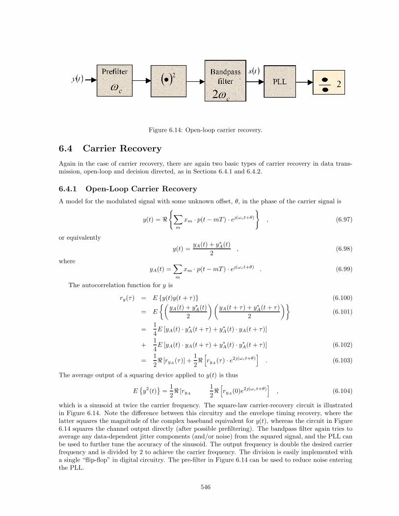
Figure 6.14: Open-loop carrier recovery.
6.4 Carrier Recovery
Again in the case of carrier recovery, there are again two basic types of carrier recovery in data trans-mission, open-loop and decision directed, as in Sections 6.4.1 and 6.4.2.
6.4.1 Open-Loop Carrier Recovery
A model for the modulated signal with some unknown offset, θ, in the phase of the carrier signal is
y(t) = <
{∑
m
xm · p(t − mT ) · e(ωct+θ)
}, (6.97)
or equivalently
y(t) =yA(t) + y∗A(t)
2, (6.98)
whereyA(t) =
∑
m
xm · p(t − mT ) · e(ωct+θ) . (6.99)
The autocorrelation function for y is
ry(τ ) = E {y(t)y(t + τ )} (6.100)
= E
{(yA(t) + y∗A(t)
2
)(yA(t + τ ) + y∗A(t + τ )
2
)}(6.101)
=14E [yA(t) · y∗A(t + τ ) + y∗A(t) · yA(t + τ )]
+14E [yA(t) · yA(t + τ ) + y∗A(t) · y∗A(t + τ )] (6.102)
=12< [ryA(τ )] +
12<
[ryA(τ ) · e2(ωct+θ)
]. (6.103)
The average output of a squaring device applied to y(t) is thus
E{y2(t)
}=
12< [ryA(0)] +
12<
[ryA(0)e2(ωct+θ)
], (6.104)
which is a sinusoid at twice the carrier frequency. The square-law carrier-recovery circuit is illustratedin Figure 6.14. Note the difference between this circuitry and the envelope timing recovery, where thelatter squares the magnitude of the complex baseband equivalent for y(t), whereas the circuit in Figure6.14 squares the channel output directly (after possible prefiltering). The bandpass filter again tries toaverage any data-dependent jitter components (and/or noise) from the squared signal, and the PLL canbe used to further tune the accuracy of the sinusoid. The output frequency is double the desired carrierfrequency and is divided by 2 to achieve the carrier frequency. The division is easily implemented witha single “flip-flop” in digital circuitry. The pre-filter in Figure 6.14 can be used to reduce noise enteringthe PLL.
546

Figure 6.15: Decision-directed phase error.
6.4.2 Decision-Directed Carrier Recovery
Decision-directed carrier recovery is more commonly encountered in practice than open loop carrierrecovery. The basic concept used to derive the error signal for phase locking is illustrated in Figure 6.15.The decision-device input xk is not exactly equal to the decision-device output xk. Since
xk = ak + bk ; xk = ak + bk , (6.105)
then
xk
xk=
|xk||xk|
· eφk (6.106)
=ak + bk
ak + bk
(6.107)
=
(akak + bkbk
)+
(akbk − akbk
)
a2k + b2
k
, (6.108)
which leads to the result
φk = arctanakbk − akbk
akak + bkbk
(6.109)
≈ arctan1Ex
(akbk − akbk
)(6.110)
≈ 1Ex
(akbk − akbk
)(6.111)
∝(akbk − ak bk
), (6.112)
547
with the approximation being increasingly accurate for small phase offsets. Alternatively, a look-uptable for arcsin or for arctan could be used to get a more accurate phase-error signal φk. For largeconstellations, the phase error must be smaller than that which would cause erroneous decisions mostof the time. Often, a training data pattern is used initially in place of the decisions to converge thecarrier recovery before switching to unknown data and decisions. Using known training patterns, thephase error should not exceed π in magnitude since a modulo-2π detector is implied.
6.4.3 Pilot Carrier Recovery
In pilot carrier recovery, the transmitter inserts a sinusoid of frequency equal to q/p times the the desiredcariier frequency. The PLL of Figure 6.9 can be used to recover the carrier rate at the receiver. Typically,pilots are inserted at unused frequencies in transmission. For instance, with OFDM and DMT systemsin Chapter 4, a single tone may be used for a pilot. In this case, if the timing reference and the carrierare locked in some known rational relationship, recover of one pilot supplies both signals using dividersas in Figure 6.9. In some situations, the carrier frequencies may apply outside of the modem box itself(for instance a baseband feed of a QAM signal for digital TV) to a broadcaster who elsewhere decidesthe carrier frequency (or channel) and there provides the carrier translation of frequency band). The 5pilors 802.11(a) WiFi systems also provide for the situation where the symbol clock and carrier frequencymay not appear the same even if locked because of movement in a wireless environment (leading to whatis called “Doppler Shift” of the carrier caused by relative motion). Then at least two pilots would beof value (and actually 5 are used to provide against loss of a few). The effect of jitter and noise arelargely eliminated because the PLL sees no data-dependent jitter at the pilot frequency if the receiverfilter preceding the PLL is sufficiently narrow.
548

6.5 Frame Synchronization in Data Transmission
While carrier and symbol clock may have been well established in a data transmission system, theboundary of long symbols (say in the use of the DMT systems of Chapter 4 or the GDFE systems ofChapter 5) or packets may not be known to a receiver. Such synchronization requires searching forsome known pattern or known characteristic of the transmitted waveform to derive a phase error (whichis typically measured in the number of sample periods or dimensions in error). Such synchronization,once established, is only lost if some kind of catastrophic failure of other mechanisms has occured (ordramatic sudden change in the channel) because it essentially involves counting the number of samplesfrom the recovered timing clock.
6.5.1 Autocorrelation Methods
Autocorrelation methods form the discrete channel output autocorrelation
Ryy(l) = E[yky∗k−l
]= hl ∗ h∗
−l ∗ Rxx(l) + Rnn(l) (6.113)
from channel output samples by time averaging over some interval of M samples
Ryy(l) =1M
M∑
m=1
M∑
m=1
ymy∗m−l . (6.114)
In forming such a sum, the receiver implies a knowledge of sampling times 1, ..., M . If those times are notcoincident with the corresponding (including channel delay) positions of the packet in the transmitter,then the autocorrelation function will look shifted. for instance, if a peak was expected at position l andoccurs instead at position l′, then the difference is an indication of a packet timing error. The phase errorused to drive a PLL is that difference. Typically, the VCO in this case supplies only discrete integer-number-of-sample steps. If noise is relatively small and hl is known, then one error may be sufficient tofind the packet boundary. If not, many repeated estimates of Ryy at different phase adjustments maybe tried.
There are 3 fundamental issues that affect the performance of such a scheme:
1. the knowledge of or choice of the input sequence xk,
2. the channel response’s (hk’s) effect upon the autocorrelation of the input,
3. the noise autocorrelation.
Synchronization Patterns
a synchronization patter or “synch sequence” is some known transmitted signal, typically with propertiesthat create a large peak in the autocorrelation function at the channel output at a known lag l. Typicallywith small (or eliminated) ISI, such a sequence corresponds to a white input. Simple random dataselection may often not be sufficient to guarantee a high autocorrelation peak for a short averagingperiod M . Thus, special sequences are often selected that have a such a short-term peaked time-averagedautocorrelation. A variety of sequences exist.
The most common types are between 1 and 2 cycles of a known period pattern. Pseudorandombinary sequences of degree p have period of 2p − 1 samples are those specified by their basic propertythat cyclic shifts of the sequence have each length-p binary patter (except all 0’s) once and only once.These sequences are sometimes used in the spreading patterns from CDMA methods in the appendix ofChapter 5 also. A simple linear-feedback register implementation appears there. Here in Chapter 6, theimportant property is that the autocorrelation (with binary antipodal modulation) of such sequences is
Rxx(l) ={
1 l = 0− 1
2p−1 l = 1, ..., 2p − 1 . (6.115)
549
For reasonably long p, the peak is easily recognizable if the channel output has little or no distortion. Infact, the entire recognition of the lag can be positioned as a basic Chapter 1 detection problem, whereeach of the possible input shifts of the same known training sequence is to be detected. Because all thesepatterns have the same energy and they’re almost orthogonal, a simple largest matched filter ouptut(the matched filter outputs are the computation of the autocorrelation at different time lags) with theprobability of error well understood in Chapter 1.
Another synchronization pattern that can have appeal is the so-called “chirp” sequence
xk = e2πk2/M (6.116)
which also has period M . It also has a single peak at time zero of size 1 and zero autocorrelation. It isharder to generate and requires a complex QAM baseband system, but in some sense is a perfect synchpattern.
A third alternative are the so-called “Barker codes” that are very short and not repeated and designedto still have peakiness in the face of unknown preceding and succeeding data surrounding the pattern.Such patterns may be periodically inserted in a transmission stream so that if the receiver for any reasonlost packet synchronization (or a new received came on after a first had already acquired the signal ifmore than receiver scan the same or related channels), then the calculation of autocorrelation wouldimmediatley recommence until the peak was found. An example of a good short synchronization patternis the 7-symbol Barker code, which is forinstance used with 2B1Q transmission in some symmetric DSLsystems that employ PAM modulation. This code transmits at maximum amplitude the binary pattern
+ + + − − + − (6.117)
(or its time reverse on loop 2 of HDSL systems) so M = 7 and only binary PAM is used when thissequence is inserted (which means the dmin is increase by 7 dB for a detection problem, simply because2 levels replace 4 already). This pattern has a maximum M · ˆRxx value of 7 units when aligned. The13 place autocorrelation function is
1010107010101 . (6.118)
Because there are adjacent transmissions, the minimum distance of 7 units ( may be reduced to 6 or 5,as long as the searching receiver has some idea when to look) multiplies a distance that is already 74 dBbetter than 4 level transmission. Thus, this pattern can be recoved quickly, even in a lot of noise.
Creative engineers can create patterns that will be easy to find in any given application.
The channel response
Severe ISI can cause a loss of the desired autocorrelation properties at the channel output. The usualsituation is that ISI is not so severe because other systems are already in use to reduce it by the timethat synchronization occurs. An exception would be when a receiver is looking for a training sequenceto adapt its equalizers (see Chapter 7) initially and thus, time-zero for that training is necessary. Insuch a case, the cross-correlation of the channel output with the various delayed versions of the knowntraining pattern can produce an estimate of hl,
1M
M∑
m=1
ykx∗k−l ≈ hl (6.119)
so that the channel can be identified. Then the resultant channel can be used in a maximum likelihoodsearch over the delayed patterns in the synchronization symbol to estimate best initial packet boundary.
The noise
Large or strongly correlated noise can cause the estimated autocorreleation to be poor. The entirechannel output yk should be whitened (as in Chapter 5) with a linear predictor. An adaptive whitening(linear predictor) filter may be necessary as in Chapter 7. In this case, again the cross-correlationestimate of Equation (6.119) can be used to estimate the euqivalent channel after oveall whitening andthe procedure of the previous section for ISI followed.
550

6.5.2 Searcing for the guard period or pilots
Large noise essentially requires the cross-correlation of channel output and input as in the previoussection. Repeated versions of the synch patter may be required to get acceptable acquisition of packetboundary.
551

Figure 6.16: Rob-Stuff Timing.
6.6 Pointers and Add/Delete Methods
This final section of Chapter 6 addresses the question, “well fine, but how did the source message clockget synchronized to the symbol clock?” The very question itself recognizes and presumes that a bitstream (or message stream) from some source probably does not also have a clock associated with it(some do, some don’t). The receiver of the message would also in some cases like to have that sourceclock and not the receiver’s estimates of the transmitter’s symbol and carrier clocks. Typically, thesource cannot be relied upon to supply a clock, and even if it does, the stability of that clock may notmatch the requiremens for the heavily modulated and coded transmission system of Chapters 1-5.
Generally, the source clock can be monitored and essentially passed through the monitoring of in-terface buffers that collect (or distribute) messages. Figure 6.16 illustrates the situation where certaintolerances on the input clock of the source may be known but the symbol clock is not synchronizedand only knows the approximate bit rate it must transmit. For such situations, the transmit symbolclock must always be the higher clock, sufficiently so that even if at its lowest end of the range of speed,it still exceeds the transmit clock. To match the two clocks, regularly inserted “dummy” messages orbits are sometimes not sent to reduce the queue depth awaiting transfer. These methods are known as“rob/stuff” or “add/delete” timing and sychronization methods.
The principle is simple. The buffer depth is monitored by subtracting the addresses of the next-to-transmit and last-in bits. If this depth is reducing or steady while above a safety threshold, then dummybits are used and transmitted. If the depth starts to increase, then dummy bits are not transmitteduntil the queue depth exceeds a threshold.
The same process occurs at the receiver interface to the “sink” of the messages. The sink must beable to receive at least the data rate of the link and typically robs or stuffs are used to accelerate or slowthe synch clock. A buffer is used in the same way. The sink’s lowest clock frequency must be within therange of the highest output clock of the receiver in the transmission system.
The size of the queue in messages (or bits) needs to be at least as large as the maximum expecteddifference in source and transmit bit-rate (or message-rate) speeds times the the time period betweenpotential dummy deletions, which are known as “robs.” (‘Stuffs are the usual dummies transmitted).The maximum speed of the transmission system with all robs must exceed the maximum source supplyof messages or bits.
Add/drop or Add/delete methods are essentially the same and typically used in what are known asasynchronous networks (like ATM for Asynchronous Transfer Mode, which is really not asynchronous
552

at all at the physically layer but does have gaps between packets that carry dummy data that is ignoredand not passed through the entire system. ATM networks typically do pass an 8 kHz network clockreference throughout the entire system. This is done with a “pointer.” The pointer typically is a positionin a high-speed stream of ATM packets that says “the difference in time between this pointer and thelast one you received is exactly 125 µs of the desired network clock. Various points along the entire pathcan then use the eventual received clock time at which that pointer was received to synchronize to thenetwork clock. If the pointer arrives sooner than expected, the locally generated network reference istoo slow and the phase error of the PLL is negative; if arrival is late, the phase error is positive.
553

Exercises - Chapter 5
6.1 Phase locked loop error induction.
a. (1 pt)
Use the D-transform equationΘ(D)Θ(D)
=αD
1 − (1 − α)D
to conclude thatθk+1 = θk + αφk
where φk = θk − θk.
b. (3 pts)
Use your result above to show by induction that when θk = θ0 and θ0 = 0, we have:
φk = (1 − αk)kθ0.
Note that this was shown another way on page 18 of Chapter 5.
c. (3 pts)
Use the result of part (a) to show (again by induction) that when θk = θ0 + k∆ and θ0 = 0, wehave:
φk = (1 − αk)kθ0 + ∆k−1∑
n=0
(1 − α)n.
This confirms the result of equation 5.49 that φk converges to ∆/α.
6.2 Second order PLL update equations.Starting from the transfer function for the phase prediction, we will derive the second order phase
locked loop update equations.
a. (2 pts) Using only the transfer function
Θ(D)Θ(D)
=(α + β)D − αD2
1 − (2 − α − β)D + (1 − α)D2
show thatΦ(D)Θ(D)
=(1 − D)2
(α + β)D − αD2.
Recall that φk = θk − θk.
b. (2 pts) Use the above result to show that
Θ(D) = DΘ(D) + αDΦ(D) +DβΦ(D)1 − D
.
c. (3 pts)
Now, defining (as in the notes)
∆(D) =βΦ(D)1 − D
show that
θk = θk−1 + αφk−1 + ∆k−1 (6.120)∆k = ∆k−1 + βφk. (6.121)
554

6.3 PLL Frequency Offset - Final 1996A discrete-time PLL updates at 10 MHz and has a local oscillator frequency of 1 MHz. This PLL
must try to phase lock to an almost 1 MHz sinusoid that may differ by 100 ppm (parts per million - soequivlaently a .01% difference in frequency). A first-order filter is used with α as given in this chapter.The phase error in steady-state operation of this PLL should be no more than .5% (.01π).
a. Find the value of α that ensures |φ| < .01(π). (2 pts)
b. Is this PLL stable if the 1 MHz is changed to 10 GHz? (1 pt)
c. Suppose this PLL were unstable - how could you fix part b without using to a 2nd-order filter? (2pts)
6.4 First-order PLL - Final 1995A receiver samples channel output y(t) at rate 2/T , where T is the transmitter symbol period. This
receiver only needs the clock frequency (not phase) exactly equal to 2/T , so a first-order PLL withconstant phase error would suffice for timing recovery. (update rate of the PLL is 400 kHz)
The transmit symbol rate is 400 kHz ±50 ppm. The receiver VCXO is 800 kHz ±50 ppm.
a. Find the greatest frequency difference of the transmit 2/T and the receiver 2/T .
b. Find the smallest value of the FOPLL α that prevents cycle slipping.
c. Repeat part b if the transmit clock accuracy and VCO accuracy are 1%, instead of 50 ppm. Suggesta potential problem with the PLL in this case.
6.5 Phase HitsA phase hit is a sudden change in the phase of a modulated signal, which can be modeled as a step-
phase input into a phase-lock loop, without change in the frequency before or after the step in phase.Let a first-order discrete-time PLL operate with a sampling rate of 1 kHz (i.e., correct phase errors arecorrectly supplied somehow 1000 times per second) on a sinusoid at frequency approximately 640 Hz,which may have phase hits. Quick reaction to a phase hit unfortunately also forces the PLL to magnifyrandom noise, so there is a trade-off between speed of reaction and noise immunity.
a. What is the maximum phase-hit magnitude (in radians) with which the designer must be con-cerned? (1 pt)
b. What value of the PLL parameter α will allow convergence to a 1% phase error (this means thephase offset on the 640 Hz signal is less than .02π) in just less than 1 s? Assume the value youdetermine is just enough to keep over-reaction to noise under control with this PLL. (2 pts)
c. For the α in part b, find the steady-state maximum phase error if the both the local oscillator andthe transmitted clock each individually have 50 ppm accuracy (hint: the analysis for this part isindependent of the phase hit)? What percent of the 640 Hz sinusoid’s period is this steady-statephase error? (2 pts)
d. How might you improve the overall design of the phase lock loop in this problem so that the 1%phase error (or better) is maintained for both hits (after 1s) and for steady-state phase error,without increasing noise over-reaction? (1 pt)
6.6 PLL - Final 2003 - 8 ptsA square-law timing recovery system with symbol rate 1/T = 1 produces a sinousoid with a jitery
or noisy phase of θ = ∆0 · k + θ0 + nk where nk is zero-mean Gaussian with variance σ2θ .
a. If a FO PLL with parameter α is used, what is a formula for E[θinfty
]? (1 pt)
b. What is a formula for the mean-square steady-state value of this FO PLL phase error? (1 pt)
555

c. If the symbol-time sampling error ε is small compared to a symbol interval so that e2πfε ≈ 1+2πfεfor all frequencies of interest, what largest value of ε would insure less than .1 dB degradation inan equalizer/receiver output error of 13.5 dB? (2 pts)
d. With ∆ = .1 and σ2θ = (.005 · 2π)2, is there a value of the FO PLL for which the SNR is satisfied
in part b? If so, what is it? (1 pt)
e. Propose a better design. Try to estimate the new phase-error variance of your design. (3 pts)
The next 4 problems are courtesy of 2006 EE379A student Jason Allen.
6.7 Frequency offset study- 10 ptsA data signal is multiplied by a sinusoidal carrier with a frequency fc to be transmitted over a
wireless communications channel. At the receiver this multiplication must be reversed to recover thebaseband data signal. Ideally such recovery can be accomplished by multiplying the received data signalby a locally generated sinusoid whose frequency is also fc Hz, and whose phase is identical to that ofthe carrier signal used at the transmitter. After passing the resultant signal through a lowpass filter,the original signal is recovered. In reality, the locally generated sinusoid will contain both a frequencyand a phase offset. Let
fLO,Rx = fLO,Tx + ∆f
represent the Local Oscillator (LO) at the receiver where ∆f represents the frequency offset betweenfLO,Rx and fLO,Tx. Ignoring the phase offset and using your basic knowledge of frequency mixing, find:
a. fsum, the frequency of the sum-frequency term (sometimes called the “sum image”). (1 pt)
b. fdiff , the frequency of the difference image. (1 pt)
c. What are the results after lowpass filtering? (2 pts)
d. Is the downconverted data signal still at baseband? (1 pt)
e. Denoting the transmitted signal as x(t) with an equivalent Fourier transform of X(f), the “near-baseband” signal can be denoted as X(f − ∆f). What is the time domain representation of the“near-baseband” signal? (2 pts)
f. What effect will this have on the data signal’s constellation? (1 pt)
g. Will this effect on the data signal constellation also effect the best symbol-by-symbol decisiondevice (slicer)? (2 pts)
6.8 Quadrature Detector- 5 pts
a. Let x(t) be a quadrature input sinusoid given by
x(t) = cos(θx(t)) + jsin(θx(t))
and y(t) be the locally generated sinusoid given by
y(t) = cos(θy (t)) − jsin(θy(t))
A quadrature phase detector generates its error by multiplying the two signals together and takingthe imaginary part of the output. Find the error signal for the given signals.
6.9 3rd Order Loops - 12 ptsUsing the transfer function given in Equation 6.17 for the phase error and input phase, explore the
outcomes of the following situations:
556

Figure 6.17: Block Diagram for Problem 6.9
a. Given a phase lock loop that has converged, how will this PLL respond to a phase step? Fromhow large of a phase step can a PLL recover? (2 pts)
b. What is the effect on a locked PLL system when there is a jump in the input signal’s frequency?(2 pts)
c. For the result of part b, show how a 1st- and 2nd-order PLL would effect the response of the systemby substituting the values for kvco · F (s) given in Figure 6.7. (2 pts)
d. In situations where the transmitter or receiver (or both) are moving with respect to each other,a Doppler Effect is seen by the PLL as a changing frequency per time, or as a frequency ramp.What is the effect of this change to the input signal on a converged PLL? (2 pts)
e. Design a Loop Filter for a 3rd-Order PLL and show what effect it has in mitigating the error foundin part d. (4 pts)
6.10 Blue Tooth PLL - 8 pts“Bluetooth” is a wireless communication standard that was developed to support short-range voice
and data transfer between portable devices. Figure ?? shows a simplified system diagram of a Bluetoothradio. In the United States, Bluetooth utilizes the Industrial Scientific Medicine (ISM) band between2.4 - 2.4835 GHz split into channels 0 - 79.
a. If channel 0 is at 2.402 GHz and channel 79 is at 2.481 GHz, what is the channel spacing in theBluetooth standard? (1 pt)
b. Assuming the VCO has an operating voltage of 0 - 3.3 volts, what tuning slope is required to coverthe stated ISM band range? (2 pts)
557

c. Referring to the divider in Figure ??, explain what effect a change in the value N would have onthis system. (2 pts)
d. Since the ISM band is a generally unlicensed band, the FCC limits the permissible power outputto 0 dBm. In order to extend the range of Bluetooth transmissions (i.e., increase the outputpower) as well as to compensate for interference from other signals in the band, Bluetooth utilizesa frequency hopping spread spectrum signal (FHSS) technique with a hop speed of 1,600 hops persecond. Since the power is now spread over the entire spectrum, the power output can be as highas 20 dBm thus extending the range of communications up to 100m as well as providing a sourceof security against interference.
From part b, assume that a microcontroller is used to store the hop sequence and implements thefrequency hopping by changing the value N of the divider. Why is the settling time of the PLLimportant? Assuming that one VCO does in fact cover the entire needed band, when would theworst-case settling time occur? (2 pts)
e. Extra Credit: Where does the name Bluetooth come from? (1 pt)
558