6 pin dip phototransistor cny17-x series photocoupler ... · document no:dpc-0000038 rev.5...
TRANSCRIPT

6 PIN DIP PHOTOTRANSISTOR PHOTOCOUPLER
Everlight Electronics Co., Ltd. 1 http:\\www.everlight.com Document No:DPC-0000038 Rev.5 December 28, 2009
CNY17-X SeriesCNY17F-X Series
Features
• Current transfer ratios in selected narrow range groups CNY17-1, CNY17F-1: 40-80% CNY17-2, CNY17F-2: 63-125% CNY17-3, CNY17F-3: 100-200% CNY17-4, CNY17F-4:160-320% • High isolation voltage between input and output (Viso = 5000 Vrms) • Creepage distance > 7.6 mm • Operating temperature up to +110°C • The CNY17F-X series offers no external base connection for minimum noise susceptibility • Compact dual-in-line package • Pb free and RoHS compliant. • UL approved (No. E214129) • VDE approved (No. 132249) • SEMKO approved • NEMKO approved • DEMKO approved • FIMKO approved • CSA approved Schematic
Description The CNY17-X and CNY17F-X series of devices each consist of an infrared emitting diode optically coupled to a phototransistor. CNY17-X
Ipackaged in a 6-pin DIP package and available in wide-lead spacing and SMD option. 1. Anode
2. Cathode 3. No Connection 4. Emitter 5. Collector 6. Base
Applications
• Power supply regulators • Digital logic inputs • Microprocessor inputs
CNY17F-X
1. Anode 2. Cathode 3. No Connection 4. Emitter 5. Collector 6. No Connection
6 PIN DIP PHOTOTRANSISTOR PHOTOCOUPLER
Everlight Electronics Co., Ltd. 2 http:\\www.everlight.com Document No:DPC-0000038 Rev.5 December 28, 2009
CNY17-X SeriesCNY17F-X Series
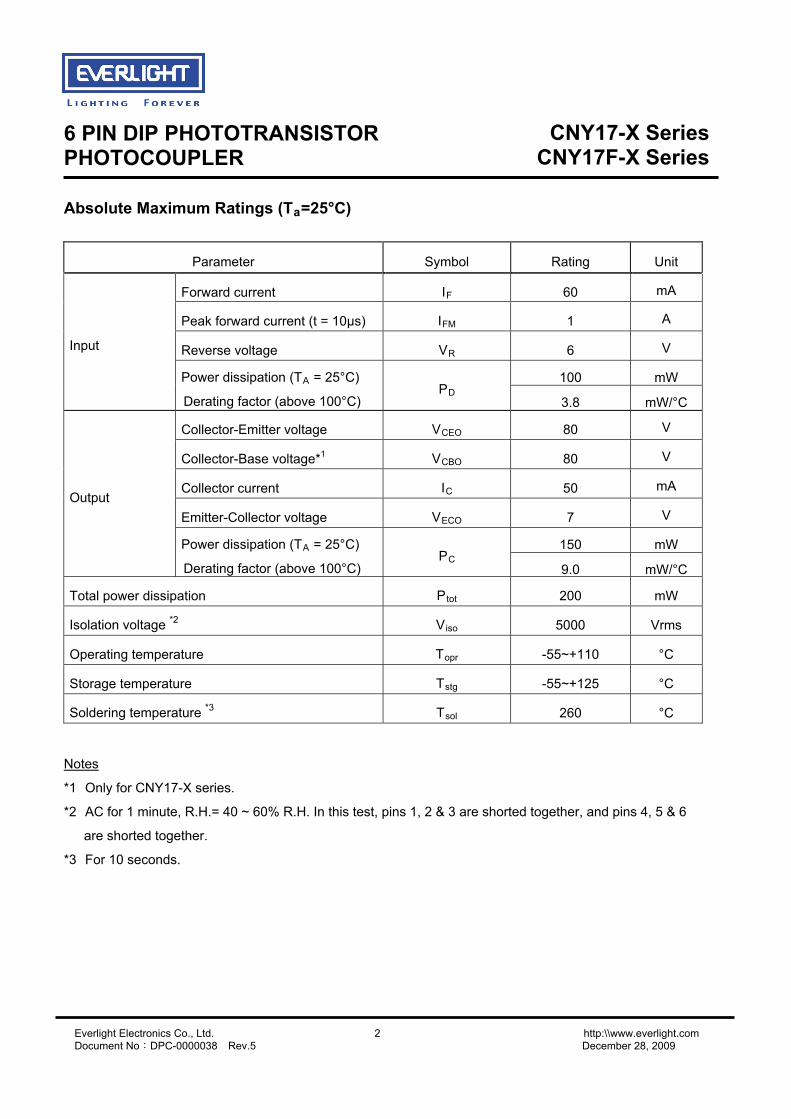
Absolute Maximum Ratings (Ta=25°C)
Parameter Symbol Rating Unit
Forward current IF 60 mA
Peak forward current (t = 10µs) IFM 1 A
Reverse voltage VR 6 V
100 mW
Input
Power dissipation (TA = 25°C)
Derating factor (above 100°C) PD
3.8 mW/°C
Collector-Emitter voltage VCEO 80 V
Collector-Base voltage*1 VCBO 80 V
Collector current IC 50 mA
Emitter-Collector voltage VECO 7 V
150 mW
Output
Power dissipation (TA = 25°C)
Derating factor (above 100°C) PC
9.0 mW/°C
Total power dissipation Ptot 200 mW
Isolation voltage *2 Viso 5000 Vrms
Operating temperature Topr -55~+110 °C
Storage temperature Tstg -55~+125 °C
Soldering temperature *3 Tsol 260 °C
Notes
*1 Only for CNY17-X series.
*2 AC for 1 minute, R.H.= 40 ~ 60% R.H. In this test, pins 1, 2 & 3 are shorted together, and pins 4, 5 & 6
are shorted together.
*3 For 10 seconds.

6 PIN DIP PHOTOTRANSISTOR PHOTOCOUPLER
Everlight Electronics Co., Ltd. 3 http:\\www.everlight.com Document No:DPC-0000038 Rev.5 December 28, 2009
CNY17-X SeriesCNY17F-X Series
Electrical Characteristics (Ta=25°C unless specified otherwise)
Input
Parameter Symbol Min. Typ.* Max. Unit Condition
Forward voltage VF - - 1.65 V IF = 60mA
Reverse current IR - - 10 µA VR = 6V
Input capacitance Cin - 18 - pF V = 0, f = 1MHz
Output
Parameter Symbol Min. Typ.* Max. Unit Condition
Collector-Base dark current
CNY17-X only ICBO - - 20 nA VCB = 10V, IF = 0mA
Collector-Emitter dark current ICEO - - 50 nA VCE = 10V, IF = 0mA
Collector-Emitter breakdown voltage BVCEO 80 - - V IC = 1mA, IF = 0mA
Collector-Base breakdown voltage
CNY17-X only BVCBO 80 - - V IC = 0.1mA, IF = 0mA
Emitter-Collector breakdown voltage BVECO 7 - - V IE = 0.1mA, IF = 0mA
Collector-Emitter capacitance CCE - 8 - pF VCE = 0V, f = 1MHz * Typical values at Ta = 25°C

6 PIN DIP PHOTOTRANSISTOR PHOTOCOUPLER
Everlight Electronics Co., Ltd. 4 http:\\www.everlight.com Document No:DPC-0000038 Rev.5 December 28, 2009
CNY17-X SeriesCNY17F-X Series
Transfer Characteristics (Ta=25°C unless specified otherwise)
Parameter Symbol Min. Typ.* Max. Unit Condition
CNY17-1 CNY17F-1 40 - 80
CNY17-2 CNY17F-2 63 - 125
CNY17-3 CNY17F-3 100 - 200
Current Transfer Ratio
CNY17-4 CNY17F-4
CTR
160 - 320
% IF = 10mA ,VCE = 5V
CNY17-1 CNY17F-1 13 - -
CNY17-2 CNY17F-2 22 - -
CNY17-3 CNY17F-3 34 - -
Current Transfer Ratio
CNY17-4 CNY17F-4
CTR
56 - -
% IF = 1mA ,VCE = 5V
Collector-Emitter saturation voltage VCE(sat) - - 0.3 V IF = 10mA , IC = 2.5mA
Isolation resistance RIO 1011 - - Ω VIO = 500Vdc
Input-output capacitance CIO - 0.5 - pF VIO = 0, f = 1MHz
Turn-on time Ton - 10 12
Turn-off time Toff - 9 12
Rise time Tr - 6 10
Fall time Tf - 8 10
VCC = 10V, IC = 2mA, RL = 100Ω See Fig. 11
Rise time Tr - 2 10
Fall time Tf - 3 10
µs
VCC = 5V, IF = 10mA,
RL = 75Ω, See Fig. 11 * Typical values at Ta = 25°C

6 PIN DIP PHOTOTRANSISTOR PHOTOCOUPLER
Everlight Electronics Co., Ltd. 5 http:\\www.everlight.com Document No:DPC-0000038 Rev.5 December 28, 2009
CNY17-X SeriesCNY17F-X Series
Typical Performance Curves

6 PIN DIP PHOTOTRANSISTOR PHOTOCOUPLER
Everlight Electronics Co., Ltd. 6 http:\\www.everlight.com Document No:DPC-0000038 Rev.5 December 28, 2009
CNY17-X SeriesCNY17F-X Series
Figure 11. Switching Time Test Circuit & Waveforms
IF IC RL
RIN
RB
VCC
Output
Input
Input Pulse
10%OutputPulse 90%
t tr fton toff

6 PIN DIP PHOTOTRANSISTOR PHOTOCOUPLER
Everlight Electronics Co., Ltd. 7 http:\\www.everlight.com Document No:DPC-0000038 Rev.5 December 28, 2009
CNY17-X SeriesCNY17F-X Series
Order Information Part Number
CNY17-XY(Z)-V or
CNY17F-XY(Z)-V Note X = Part no. (1, 2, 3 or 4) Y = Lead form option (S, S1, M or none) Z = Tape and reel option (TA, TB or none). V = VDE (optional)
Option Description Packing quantity
None Standard DIP-6 65 units per tube
M Wide lead bend (0.4 inch spacing) 65 units per tube
S (TA) Surface mount lead form + TA tape & reel option 1000 units per reel
S (TB) Surface mount lead form + TB tape & reel option 1000 units per reel
S1 (TA) Surface mount lead form (low profile) + TA tape & reel option 1000 units per reel
S1 (TB) Surface mount lead form (low profile) + TB tape & reel option 1000 units per reel

6 PIN DIP PHOTOTRANSISTOR PHOTOCOUPLER
Everlight Electronics Co., Ltd. 8 http:\\www.everlight.com Document No:DPC-0000038 Rev.5 December 28, 2009
CNY17-X SeriesCNY17F-X Series
Package Drawings (Dimensions in mm)
Standard DIP Type
Option M Type
6 PIN DIP PHOTOTRANSISTOR PHOTOCOUPLER
Everlight Electronics Co., Ltd. 9 http:\\www.everlight.com Document No:DPC-0000038 Rev.5 December 28, 2009
CNY17-X SeriesCNY17F-X Series
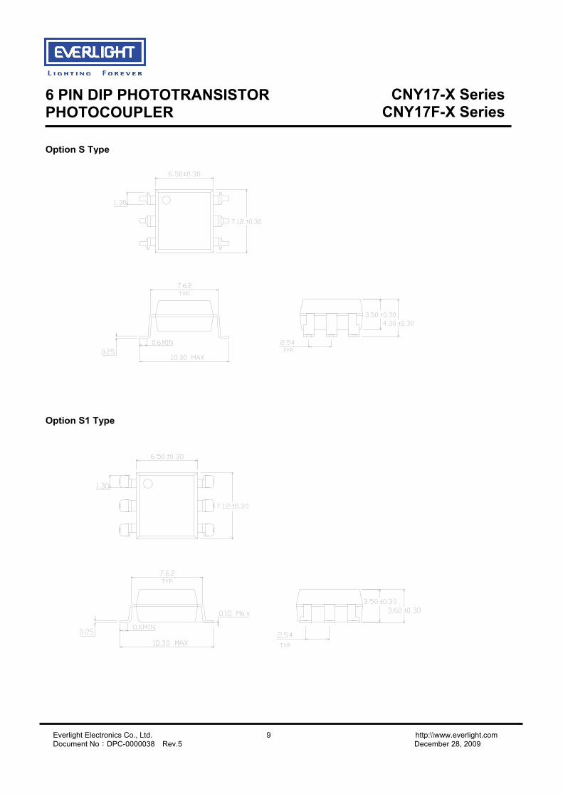
Option S Type
Option S1 Type

6 PIN DIP PHOTOTRANSISTOR PHOTOCOUPLER
Everlight Electronics Co., Ltd. 10 http:\\www.everlight.com Document No:DPC-0000038 Rev.5 December 28, 2009
CNY17-X SeriesCNY17F-X Series
Recommended pad layout for surface mount leadform
Device Marking
YW W V
ELCNY17-X
Notes EL denotes Everlight CNY17-X denotes Device Number (X: 1, 2, 3 or 4) Y denotes 1 digit Year code WW denotes 2 digit Week code V denotes VDE (optional)

6 PIN DIP PHOTOTRANSISTOR PHOTOCOUPLER
Everlight Electronics Co., Ltd. 11 http:\\www.everlight.com Document No:DPC-0000038 Rev.5 December 28, 2009
CNY17-X SeriesCNY17F-X Series
Tape & Reel Packing Specifications
Tape dimensions
Option TA Option TB
Direction of feed from reel Direction of feed from reel
Dimension No. A B Do D1 E F
Dimension (mm) 10.4±0.1 7.52±0.1 1.5±0.1 1.5+0.1/-0 1.75±0.1 7.5±0.1
Dimension No. Po P1 P2 t W K
Dimension (mm) 4.0±0.15 16.0±0.1 2.0±0.1 0.35±0.03 16.0±0.2 4.5±0.1

6 PIN DIP PHOTOTRANSISTOR PHOTOCOUPLER
Everlight Electronics Co., Ltd. 12 http:\\www.everlight.com Document No:DPC-0000038 Rev.5 December 28, 2009
CNY17-X SeriesCNY17F-X Series
Solder Reflow Temperature Profile
260 °C ( ) peak,10 Sec Max
150°C
1-3 °C/Sec Max
70 – 170 Sec
200°C
217°C
>255 °C ( 30s Max )
1-3 °C/Sec Max60 – 140 Sec
TIME (S)

6 PIN DIP PHOTOTRANSISTOR PHOTOCOUPLER
Everlight Electronics Co., Ltd. 13 http:\\www.everlight.com Document No:DPC-0000038 Rev.5 December 28, 2009
CNY17-X SeriesCNY17F-X Series
DISCLAIMER 1. Above specification may be changed without notice. EVERLIGHT will reserve authority on material change
for above specification. 2. When using this product, please observe the absolute maximum ratings and the instructions for use
outlined in these specification sheets. EVERLIGHT assumes no responsibility for any damage resulting
from use of the product which does not comply with the absolute maximum ratings and the instructions
included in these specification sheets.
3. These specification sheets include materials protected under copyright of EVERLIGHT. Reproduction in
any form is prohibited without the specific consent of EVERLIGHT.