60mhz, rail-to-rail output, 1.9nv/ offset voltage match (channel-to-channel) (note 6) 80 600 µv ib...
TRANSCRIPT
1623345fc
LT6233/LT6233-10LT6234/LT6235
Typical applicaTion
FeaTures DescripTion
60MHz, Rail-to-Rail Output,1.9nV/√Hz, 1.2mA Op Amp Family
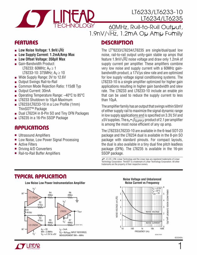
Low Noise Low Power Instrumentation Amplifier
applicaTions
n Low Noise Voltage: 1.9nV/√Hzn Low Supply Current: 1.2mA/Amp Maxn Low Offset Voltage: 350µV Maxn Gain-Bandwidth Product: LT6233: 60MHz; AV ≥ 1 LT6233-10: 375MHz; AV ≥ 10n Wide Supply Range: 3V to 12.6Vn Output Swings Rail-to-Railn Common Mode Rejection Ratio: 115dB Typn Output Current: 30mAn Operating Temperature Range: –40°C to 85°Cn LT6233 Shutdown to 10µA Maximumn LT6233/LT6233-10 in a Low Profile (1mm)
ThinSOT™ Packagen Dual LT6234 in 8-Pin SO and Tiny DFN Packagesn LT6235 in a 16-Pin SSOP Package
n Ultrasound Amplifiersn Low Noise, Low Power Signal Processingn Active Filtersn Driving A/D Convertersn Rail-to-Rail Buffer Amplifiers
L, LT, LTC, LTM, Linear Technology and the Linear logo are registered trademarks of Linear Technology Corporation. ThinSOT is a trademark of Linear Technology Corporation. All other trademarks are the property of their respective owners.
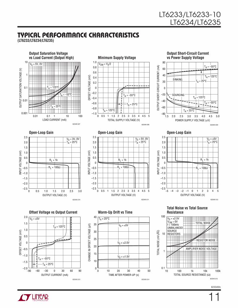
Noise Voltage and UnbalancedNoise Current vs Frequency
The LT®6233/LT6234/LT6235 are single/dual/quad low noise, rail-to-rail output unity-gain stable op amps that feature 1.9nV/√Hz noise voltage and draw only 1.2mA of supply current per amplifier. These amplifiers combine very low noise and supply current with a 60MHz gain-bandwidth product, a 17V/µs slew rate and are optimized for low supply voltage signal conditioning systems. The LT6233-10 is a single amplifier optimized for higher gain applications resulting in higher gain bandwidth and slew rate. The LT6233 and LT6233-10 include an enable pin that can be used to reduce the supply current to less than 10µA.
The amplifier family has an output that swings within 50mV of either supply rail to maximize the signal dynamic range in low supply applications and is specified on 3.3V, 5V and ±5V supplies. The en • √ISUPPLY product of 2.1 per amplifier is among the most noise efficient of any op amp.
The LT6233/LT6233-10 are available in the 6-lead SOT-23 package and the LT6234 dual is available in the 8-pin SO package with standard pinouts. For compact layouts, the dual is also available in a tiny dual fine pitch leadless package (DFN). The LT6235 is available in the 16-pin SSOP package.
R6499Ω
VS+
AV = 20BW = 2.8MHzVS = ±1.5V to ±5V
VOUT
VS–
IN+
IN–
VS–
VS+
R7499Ω
R4499Ω
R2475Ω
R149.9Ω
R3475Ω R5
499Ω
EN
IS = 3mAEN = 8µVRMS INPUT REFERRED,MEASUREMENT BW = 4MHz
623345 TA01a
–
+LT6233
1/2 LT6234
1/2 LT6234
FREQUENCY (Hz)
NOIS
E VO
LTAG
E (n
V/√H
z)
6
5
4
3
2
1
010 1k 10k 100k
623345 TA01b
100
VS = ±2.5VTA = 25°CVCM = 0V
NOISE VOLTAGE
NOISE CURRENT
UNBALANCED NOISE CURRENT (pA/√Hz)
6
5
4
3
2
1
0
LT6233/LT6233-10LT6234/LT6235
2623345fc
absoluTe MaxiMuM raTingsTotal Supply Voltage (V+ to V–) .............................. 12.6VInput Current (Note 2) ......................................... ±40mAOutput Short-Circuit Duration (Note 3) ............ IndefiniteOperating Temperature Range (Note 4)....–40°C to 85°CSpecified Temperature Range (Note 5) ....–40°C to 85°CJunction Temperature ........................................... 150°C
(Note 1)
6 V+
5 ENABLE
4 –IN
OUT 1
TOP VIEW
S6 PACKAGE6-LEAD PLASTIC TSOT-23
V– 2
+IN 3
TJMAX = 150°C, θJA = 250°C/W
TOP VIEW
DD PACKAGE8-LEAD (3mm × 3mm) PLASTIC DFN
5
6
7
8
4
3
2
1OUT A
–IN A
+IN A
V–
V+
OUT B
–IN B
+IN B
+–
+–
TJMAX = 125°C, θJA = 160°C/W
UNDERSIDE METAL CONNECTED TO V– (PCB CONNECTION OPTIONAL)
TOP VIEW
V+
OUT B
–IN B
+IN B
OUT A
–IN A
+IN A
V–
S8 PACKAGE8-LEAD PLASTIC SO
1
2
3
4
8
7
6
5
+–
+–
TJMAX = 150°C, θJA = 190°C/W
TOP VIEW
GN PACKAGE16-LEAD NARROW PLASTIC SSOP
1
2
3
4
5
6
7
8
16
15
14
13
12
11
10
9
OUT A
–IN A
+IN A
V+
+IN B
–IN B
OUT B
NC
OUT D
–IN D
+IN D
V–
+IN C
–IN C
OUT C
NC
+
–
+
–
+
–+
–
A D
B C
TJMAX = 150°C, θJA = 135°C/W
pin conFiguraTion
Junction Temperature (DD Package) .................... 125°CStorage Temperature Range .................. –65°C to 150°CStorage Temperature Range (DD Package) ........................................ –65°C to 125°CLead Temperature (Soldering, 10 sec) ................... 300°C

3623345fc
LT6233/LT6233-10LT6234/LT6235
elecTrical characTerisTics TA = 25°C, VS = 5V, 0V; VS = 3.3V, 0V; VCM = VOUT = half supply, ENABLE = 0V, unless otherwise noted.
orDer inForMaTionLEAD FREE FINISH TAPE AND REEL PART MARKING* PACKAGE DESCRIPTION SPECIFIED TEMPERATURE RANGE
LT6233CS6#PBF LT6233CS6#TRPBF LTAFL 6-Lead Plastic TS0T-23 0°C to 70°C
LT6233IS6#PBF LT6233IS6#TRPBF LTAFL 6-Lead Plastic TS0T-23 –40°C to 85°C
LT6233CS6-10#PBF LT6233CS6-10#TRPBF LTAFM 6-Lead Plastic TS0T-23 0°C to 70°C
LT6233IS6-10#PBF LT6233IS6-10#TRPBF LTAFM 6-Lead Plastic TS0T-23 –40°C to 85°C
LT6234CS8#PBF LT6234CS8#TRPBF 6234 8-Lead Plastic SO 0°C to 70°C
LT6234IS8#PBF LT6234IS8#TRPBF 6234I 8-Lead Plastic SO –40°C to 85°C
LT6234CDD#PBF LT6234CDD#TRPBF LAET 8-Lead (3mm × 3mm) Plastic DFN 0°C to 70°C
LT6234IDD#PBF LT6234IDD#TRPBF LAET 8-Lead (3mm × 3mm) Plastic DFN –40°C to 85°C
LT6235CGN#PBF LT6235CGN#TRPBF 6235 16-Lead Narrow Plastic SSOP 0°C to 70°C
LT6235IGN#PBF LT6235IGN#TRPBF 6235I 16-Lead Narrow Plastic SSOP –40°C to 85°C
Consult LTC Marketing for parts specified with wider operating temperature ranges. *The temperature grade is identified by a label on the shipping container.Consult LTC Marketing for information on non-standard lead based finish parts.For more information on lead free part marking, go to: http://www.linear.com/leadfree/ For more information on tape and reel specifications, go to: http://www.linear.com/tapeandreel/
SYMBOL PARAMETER CONDITIONS MIN TYP MAX UNITS
VOS Input Offset Voltage LT6233S6, LT6233S6-10 LT6234S8, LT6235GN LT6234DD
100 50 75
500 350 450
µV µV µV
Input Offset Voltage Match (Channel-to-Channel) (Note 6)
80 600 µV
IB Input Bias Current 1.5 3 µA
IB Match (Channel-to-Channel) (Note 6) 0.04 0.3 µA
IOS Input Offset Current 0.04 0.3 µA
Input Noise Voltage 0.1Hz to 10Hz 220 nVP-P
en Input Noise Voltage Density f = 10kHz, VS = 5V 1.9 3 nV/√Hz
in Input Noise Current Density, Balanced Source Input Noise Current Density, Unbalanced Source
f = 10kHz, VS = 5V, RS = 10k f = 10kHz, VS = 5V, RS = 10k
0.43 0.78
pA/√Hz pA/√Hz
Input Resistance Common Mode Differential Mode
22 25
MΩ kΩ
CIN Input Capacitance Common Mode Differential Mode
2.5 4.2
pF pF
AVOL Large-Signal Gain VS = 5V, VO = 0.5V to 4.5V, RL = 10k to VS/2 VS = 5V, VO = 0.5V to 4.5V, RL = 1k to VS/2
73 18
140 35
V/mV V/mV
VS = 3.3V, VO = 0.65V to 2.65V, RL = 10k to VS/2 VS = 3.3V, VO = 0.65V to 2.65V, RL = 1k to VS/2
53 11
100 20
V/mV V/mV
VCM Input Voltage Range Guaranteed by CMRR, VS = 5V, 0V Guaranteed by CMRR, VS = 3.3V, 0V
1.5 1.15
4 2.65
V V
CMRR Common Mode Rejection Ratio VS = 5V, VCM = 1.5V to 4V VS = 3.3V, VCM = 1.15V to 2.65V
90 85
115 110
dB dB
CMRR Match (Channel-to-Channel) (Note 6) VS = 5V, VCM = 1.5V to 4V 84 115 dB

LT6233/LT6233-10LT6234/LT6235
4623345fc
elecTrical characTerisTics TA = 25°C, VS = 5V, 0V; VS = 3.3V, 0V; VCM = VOUT = half supply, ENABLE = 0V, unless otherwise noted.
SYMBOL PARAMETER CONDITIONS MIN TYP MAX UNITS
PSRR Power Supply Rejection Ratio VS = 3V to 10V 90 115 dB
PSRR Match (Channel-to-Channel) (Note 6) VS = 3V to 10V 84 115 dB
Minimum Supply Voltage (Note 7) 3 V
VOL Output Voltage Swing Low (Note 8) No Load ISINK = 5mA VS = 5V, ISINK = 15mA VS = 3.3V, ISINK = 10mA
4 75
165 125
40 180 320 240
mV mV mV mV
VOH Output Voltage Swing High (Note 8) No Load ISOURCE = 5mA VS = 5V, ISOURCE = 15mA VS = 3.3V, ISOURCE = 10mA
5 85
220 165
50 195 410 310
mV mV mV mV
ISC Short-Circuit Current VS = 5V VS = 3.3V
±40 ±35
±55 ±50
mA mA
IS Supply Current per Amplifier Disabled Supply Current per Amplifier
ENABLE = V+ – 0.35V
1.05 0.2
1.2 10
mA µA
IENABLE ENABLE Pin Current ENABLE = 0.3V –25 –75 µA
VL ENABLE Pin Input Voltage Low 0.3 V
VH ENABLE Pin Input Voltage High V+ – 0.35 V
Output Leakage Current ENABLE = V+ – 0.35V, VO = 1.5V to 3.5V 0.2 10 µA
tON Turn-On Time ENABLE = 5V to 0V, RL = 1k, VS = 5V 500 ns
tOFF Turn-Off Time ENABLE = 0V to 5V, RL = 1k, VS = 5V 76 µs
GBW Gain-Bandwidth Product Frequency = 1MHz, VS = 5V LT6233-10
55 320
MHz MHz
SR Slew Rate VS = 5V, A V = –1, RL = 1k, VO = 1.5V to 3.5V 10 15 V/µs
LT6233-10, VS = 5V, AV = –10, RL = 1k, VO = 1.5V to 3.5V
80 V/µs
FPBW Full-Power Bandwidth VS = 5V, VOUT = 3VP-P (Note 9) 1.06 1.6 MHz
LT6233-10, HD2 = HD3 ≤ 1% 2.2 MHz
tS Settling Time (LT6233, LT6234, LT6235) 0.1%, VS = 5V, VSTEP = 2V, AV = –1, RL = 1k 175 ns

5623345fc
LT6233/LT6233-10LT6234/LT6235
SYMBOL PARAMETER CONDITIONS MIN TYP MAX UNIT
VOS Input Offset Voltage LT6233CS6, LT6233CS6-10 LT6234CS8, LT6235CGN LT6234CDD
l
l
l
600 450 550
µV µV µV
Input Offset Voltage Match (Channel-to-Channel) (Note 6)
l 800 µV
VOS TC Input Offset Voltage Drift (Note 10) VCM = Half Supply l 0.5 3.0 µV/°C
IB Input Bias Current l 3.5 µA
IB Match (Channel-to-Channel) (Note 6) l 0.4 µA
IOS Input Offset Current l 0.4 µA
AVOL Large-Signal Gain VS = 5V, VO = 0.5V to 4.5V, RL = 10k to VS/2 VS = 5V, VO = 0.5V to 4.5V, RL = 1k to VS/2
l
l
47 12
V/mV V/mV
VS = 3.3V, VO = 0.65V to 2.65V, RL = 10k to VS/2 VS = 3.3V, VO = 0.65V to 2.65V, RL = 1k to VS/2
l
l
40 7.5
V/mV V/mV
VCM Input Voltage Range Guaranteed by CMRR VS = 5V, 0V Vs = 3.3V, 0V
l
l
1.5
1.15
4
2.65
V V
CMRR Common Mode Rejection Ratio VS = 5V, VCM = 1.5V to 4V VS = 3.3V, VCM = 1.15V to 2.65V
l
l
90 85
dB dB
CMRR Match (Channel-to-Channel) (Note 6) VS = 5V, VCM = 1.5V to 4V l 84 dB
PSRR Power Supply Rejection Ratio VS = 3V to 10V l 90 dB
PSRR Match (Channel-to-Channel) (Note 6) VS = 3V to 10V l 84 dB
Minimum Supply Voltage (Note 7) l 3 V
VOL Output Voltage Swing Low (Note 8) No Load ISINK = 5mA VS = 5V, ISINK = 15mA VS = 3.3V, ISINK = 10mA
l
l
l
l
50 195 360 265
mV mV mV mV
VOH Output Voltage Swing High (Note 8) No Load ISOURCE = 5mA VS = 5V, ISOURCE = 15mA VS = 3.3V, ISOURCE = 10mA
l
l
l
l
60 205 435 330
mV mV mV mV
ISC Short-Circuit Current VS = 5V VS = 3.3V
l
l
±35 ±30
mA mA
IS Supply Current per Amplifier Disabled Supply Current per Amplifier
ENABLE = V+ – 0.25V
l
l
1
1.45 mA µA
IENABLE ENABLE Pin Current ENABLE = 0.3V l –85 µA
VL ENABLE Pin Input Voltage Low l 0.3 V
VH ENABLE Pin Input Voltage High l V+ – 0.25 V
Output Leakage Current ENABLE = V+ – 0.25V, VO = 1.5V to 3.5V l 1 µA
tON Turn-On Time ENABLE = 5V to 0V, RL = 1k, VS = 5V l 500 ns
tOFF Turn-Off Time ENABLE = 0V to 5V, RL = 1k, VS = 5V l 120 µs
SR Slew Rate VS = 5V, AV = –1, RL = 1k, VO = 1.5V to 3.5V l 9 V/µs
LT6233-10, AV = –10, RL = 1k, VO = 1.5V to 3.5V l 75 V/µs
FPBW Full-Power Bandwidth (Note 9) VS = 5V, VOUT = 3VP-P; LT6233C, LT6234C, LT6235C
l 955 kHz
elecTrical characTerisTics The l denotes the specifications which apply over the 0°C < TA < 70°C temperature range. VS = 5V, 0V; VS = 3.3V, 0V; VCM = VOUT = half supply, ENABLE = 0V, unless otherwise noted.

LT6233/LT6233-10LT6234/LT6235
6623345fc
elecTrical characTerisTics The l denotes the specifications which apply over the –40°C < TA < 85°C temperature range. VS = 5V, 0V; VS = 3.3V, 0V; VCM = VOUT = half supply, ENABLE = 0V, unless otherwise noted. (Note 5)
SYMBOL PARAMETER CONDITIONS MIN TYP MAX UNITS
VOS Input Offset Voltage LT6233IS6, LT6233IS6-10 LT6234IS8, LT6235IGN LT6234IDD
l
l
l
700 550 650
µV µV µV
Input Offset Voltage Match (Channel-to-Channel) (Note 6)
l 1000 µV
VOS TC Input Offset Voltage Drift (Note 10) VCM = Half Supply l 0.5 3 µV/°C
IB Input Bias Current l 4 µA
IB Match (Channel-to-Channel) (Note 6) l 0.4 µA
IOS Input Offset Current l 0.5 µA
AVOL Large-Signal Gain VS = 5V, VO = 0.5V to 4.5V, RL = 10k to VS/2 VS = 5V, VO = 0.5V to 4.5V, RL = 1k to VS/2
l
l
45 11
V/mV V/mV
VS = 3.3V, VO = 0.65V to 2.65V, RL = 10k to VS/2 VS = 3.3V, VO = 0.65V to 2.65V, RL = 1k to VS/2
l
l
38 7
V/mV V/mV
VCM Input Voltage Range Guaranteed by CMRR VS = 5V, 0V VS = 3.3V, 0V
l
l
1.5
1.15
4
2.65
V V
CMRR Common Mode Rejection Ratio VS = 5V, VCM = 1.5V to 4V VS = 3.3V, VCM = 1.15V to 2.65V
l
l
90 85
dB dB
CMRR Match (Channel-to-Channel) (Note 6) VS = 5V, VCM = 1.5V to 4V l 84 dB
PSRR Power Supply Rejection Ratio VS = 3V to 10V l 90 dB
PSRR Match (Channel-to-Channel) (Note 6) VS = 3V to 10V l 84 dB
Minimum Supply Voltage (Note 7) l 3 V
VOL Output Voltage Swing Low (Note 8) No Load ISINK = 5mA VS = 5V, ISINK = 15mA VS = 3.3V, ISINK = 10mA
l
l
l
l
50 195 370 275
mV mV mV mV
VOH Output Voltage Swing High (Note 6) No Load ISOURCE = 5mA VS = 5V, ISOURCE = 15mA VS = 3.3V, ISOURCE = 10mA
l
l
l
l
60 210 445 335
mV mV mV mV
ISC Short-Circuit Current VS = 5V VS = 3.3V
l
l
±30 ±20
mA mA
IS Supply Current per Amplifier Disabled Supply Current per Amplifier
ENABLE = V+ – 0.2V
l
l
1
1.5 mA µA
IENABLE ENABLE Pin Current ENABLE = 0.3V l –100 µA
VL ENABLE Pin Input Voltage Low l 0.3 V
VH ENABLE Pin Input Voltage High l V+ – 0.2 V
Output Leakage Current ENABLE = V+ – 0.2V, VO = 1.5V to 3.5V l 1 µA
tON Turn-On Time ENABLE = 5V to 0V, RL = 1k, VS = 5V l 500 ns
tOFF Turn-Off Time ENABLE = 0V to 5V, RL = 1k, VS = 5V l 135 µs
SR Slew Rate VS = 5V, AV = –1, RL = 1k, VO = 1.5V to 3.5V l 8 V/µs
LT6233-10, AV = –10, RL = 1k, VO = 1.5V to 3.5V l 70 V/µs
FPBW Full-Power Bandwidth (Note 9) VS = 5V, VOUT = 3VP-P; LT6233I, LT6234I, LT6235I
l 848 kHz
7623345fc
LT6233/LT6233-10LT6234/LT6235
elecTrical characTerisTics TA = 25°C, VS = ±5V, VCM = VOUT = 0V, ENABLE = 0V, unless otherwise noted.
SYMBOL PARAMETER CONDITIONS MIN TYP MAX UNITS
VOS Input Offset Voltage LT6233S6, LT6233S6-10 LT6234S8, LT6235GN LT6234DD
100 50 75
500 350 450
µV µV µV
Input Offset Voltage Match (Channel-to-Channel) (Note 6)
100 600 µV
IB Input Bias Current 1.5 3 µA
IB Match (Channel-to-Channel) (Note 6) 0.04 0.3 µA
IOS Input Offset Current 0.04 0.3 µA
Input Noise Voltage 0.1Hz to 10Hz 220 nVP-P
en Input Noise Voltage Density f = 10kHz 1.9 3.0 nV/√Hz
in Input Noise Current Density, Balanced Source Input Noise Current Density, Unbalanced Source
f = 10kHz, RS = 10k f = 10kHz, RS = 10k
0.43 0.78
pA/√Hz pA/√Hz
Input Resistance Common Mode Differential Mode
22 25
MΩ kΩ
CIN Input Capacitance Common Mode Differential Mode
2.1 3.7
pF pF
AVOL Large-Signal Gain VO = ±4.5V, RL = 10k VO = ±4.5V, RL = 1k
97 28
180 55
V/mV V/mV
VCM Input Voltage Range Guaranteed by CMRR –3 4 V
CMRR Common Mode Rejection Ratio VCM = –3V to 4V 90 110 dB
CMRR Match (Channel-to-Channel) (Note 6) VCM = –3V to 4V 84 120 dB
PSRR Power Supply Rejection Ratio VS = ±1.5V to ±5V 90 115 dB
PSRR Match (Channel-to-Channel) (Note 6) VS = ±1.5V to ±5V 84 115 dB
VOL Output Voltage Swing Low (Note 8) No Load ISINK = 5mA ISINK = 15mA
4 75
165
40 180 320
mV mV mV
VOH Output Voltage Swing High (Note 8) No Load ISOURCE = 5mA ISOURCE = 15mA
5 85
220
50 195 410
mV mV mV
ISC Short-Circuit Current ±40 ±55 mA
IS Supply Current per Amplifier Disabled Supply Current per Amplifier
ENABLE = 4.65V
1.15 0.2
1.4 10
mA µA
IENABLE ENABLE Pin Current ENABLE = 0.3V –35 –85 µA
VL ENABLE Pin Input Voltage Low 0.3 V
VH ENABLE Pin Input Voltage High 4.65 V
Output Leakage Current ENABLE = 4.65V, VO = ±1V 0.2 10 µA
tON Turn-On Time ENABLE = 5V to 0V, RL = 1k 900 ns
tOFF Turn-Off Time ENABLE = 0V to 5V, RL = 1k 100 µs
GBW Gain-Bandwidth Product Frequency = 1MHz LT6233-10
42 260
60 375
MHz MHz
SR Slew Rate AV = –1, RL = 1k, VO = –2V to 2V 12 17 V/µs
LT6233-10, AV = –10, RL = 1k, VO = –2V to 2V 115 V/µs
FPBW Full-Power Bandwidth VOUT = 3VP-P (Note 9) 1.27 1.8 MHz
LT6233-10, HD2 = HD3 ≤ 1% 2.2 MHz
tS Settling Time (LT6233, LT6234, LT6235) 0.1%, VSTEP = 2V, AV = –1, RL = 1k 170 ns

LT6233/LT6233-10LT6234/LT6235
8623345fc
elecTrical characTerisTics The l denotes the specifications which apply over the 0°C < TA < 70°C temperature range. VS = ±5V, VCM = VOUT = 0V, ENABLE = 0V, unless otherwise noted.
SYMBOL PARAMETER CONDITIONS MIN TYP MAX UNITS
VOS Input Offset Voltage LT6233CS6, LT6233CS6-10 LT6234CS8, LT6235CGN LT6234CDD
l
l
l
600 450 550
µV µV µV
Input Offset Voltage Match (Channel-to-Channel) (Note 6)
l 800 µV
VOS TC Input Offset Voltage Drift (Note 10) l 0.5 3 µV/°C
IB Input Bias Current l 3.5 µA
IB Match (Channel-to-Channel) (Note 6) l 0.4 µA
IOS Input Offset Current l 0.4 µA
AVOL Large-Signal Gain VO = ±4.5V, RL = 10k VO = ±4.5V, RL = 1k
l
l
75 22
V/mV V/mV
VCM Input Voltage Range Guaranteed by CMRR l –3 4 V
CMRR Common Mode Rejection Ratio VCM = –3V to 4V l 90 dB
CMRR Match (Channel-to-Channel) (Note 6) VCM = –3V to 4V l 84 dB
PSRR Power Supply Rejection Ratio VS = ±1.5V to ±5V l 90 dB
PSRR Match (Channel-to-Channel) (Note 6) VS = ±1.5V to ±5V l 84 dB
VOL Output Voltage Swing Low (Note 8) No Load ISINK = 5mA ISINK = 15mA
l
l
l
50 195 360
mV mV mV
VOH Output Voltage Swing High (Note 8) No Load ISOURCE = 5mA ISOURCE = 15mA
l
l
l
60 205 435
mV mV mV
ISC Short-Circuit Current l ±35 mA
IS Supply Current per Amplifier Disabled Supply Current per Amplifier
ENABLE = 4.75V
l
l
1
1.7 mA µA
IENABLE ENABLE Pin Current ENABLE = 0.3V l –95 µA
VL ENABLE Pin Input Voltage Low l 0.3 V
VH ENABLE Pin Input Voltage High l 4.75 V
Output Leakage Current ENABLE = 4.75V, VO = ±1V l 1 µA
tON Turn-On Time ENABLE = 5V to 0V, RL = 1k l 900 ns
tOFF Turn-Off Time ENABLE = 0V to 5V, RL = 1k l 150 µs
SR Slew Rate AV = –1, RL = 1k, VO = –2V to 2V l 11 V/µs
LT6233-10, AV = –10, RL = 1k, VO = –2V to 2V l 105 V/µs
FPBW Full-Power Bandwidth (Note 9) VOUT = 3VP-P ; LT6233C, LT6234C, LT6235C l 1.16 MHz

9623345fc
LT6233/LT6233-10LT6234/LT6235
elecTrical characTerisTics The l denotes the specifications which apply over the –40°C < TA < 85°C temperature range. VS = ±5V, VCM = VOUT = 0V, ENABLE = 0V, unless otherwise noted. (Note 5)
SYMBOL PARAMETER CONDITIONS MIN TYP MAX UNITS
VOS Input Offset Voltage LT6233IS6, LT6233IS6-10 LT6234IS8, LT6235IGN LT6234IDD
l
l
l
700 550 650
µV µV µV
Input Offset Voltage Match (Channel-to-Channel) (Note 6)
l 1000 µV
VOS TC Input Offset Voltage Drift (Note 10) l 0.5 3 µV/°C
IB Input Bias Current l 4 µA
IB Match (Channel-to-Channel) (Note 6) l 0.4 µA
IOS Input Offset Current l 0.5 µA
AVOL Large-Signal Gain VO = ±4.5V, RL = 10k VO = ±4.5V, RL = 1k
l
l
68 20
V/mV V/mV
VCM Input Voltage Range Guaranteed by CMRR l –3 4 V
CMRR Common Mode Rejection Ratio VCM = –3V to 4V l 90 dB
CMRR Match (Channel-to-Channel) (Note 6) VCM = –3V to 4V l 84 dB
PSRR Power Supply Rejection Ratio VS = ±1.5V to ±5V l 90 dB
PSRR Match (Channel-to-Channel) (Note 6) VS = ±1.5V to ±5V l 84 dB
VOL Output Voltage Swing Low (Note 8) No Load ISINK = 5mA ISINK = 15mA
l
l
l
50 195 370
mV mV mV
VOH Output Voltage Swing High (Note 8) No Load ISOURCE = 5mA ISOURCE = 15mA
l
l
l
70 210 445
mV mV mV
ISC Short-Circuit Current l ±30 mA
IS Supply Current per Amplifier Disabled Supply Current per Amplifier
ENABLE = 4.8V
l
l
1
1.75 mA µA
IENABLE ENABLE Pin Current ENABLE = 0.3V l –110 µA
VL ENABLE Pin Input Voltage Low l 0.3 V
VH ENABLE Pin Input Voltage High l 4.8 V
Output Leakage Current ENABLE = 4.8V, VO = ±1V l 1 µA
tON Turn-On Time ENABLE = 5V to 0V, RL = 1k l 900 ns
tOFF Turn-Off Time ENABLE = 0V to 5V, RL = 1k l 160 µs
SR Slew Rate AV = –1, RL = 1k, VO = –2V to 2V l 10 V/µs
LT6233-10, AV = –10, RL = 1k, VO = –2V to 2V l 95 V/µs
FPBW Full-Power Bandwidth (Note 9) VOUT = 3VP-P; LT6233I, LT6234I, LT6235I l 1.06 MHz
Note 1: Stresses beyond those listed under Absolute Maximum Ratings may cause permanent damage to the device. Exposure to any Absolute Maximum Rating condition for extended periods may affect device reliability and lifetime.Note 2: Inputs are protected by back-to-back diodes. If the differential input voltage exceeds 0.7V, the input current must be limited to less than 40mA.Note 3: A heat sink may be required to keep the junction temperature below the absolute maximum rating when the output is shorted indefinitely. Note 4: The LT6233C/LT6233I the LT6234C/LT6234I, and LT6235C/LT6235I are guaranteed functional over the temperature range of –40°C to 85°C.
Note 5: The LT6233C/LT6234C/LT6235C are guaranteed to meet specified performance from 0°C to 70°C. The LT6233C/LT6234C/LT6235C are designed, characterized and expected to meet specified performance from –40°C to 85°C, but are not tested or QA sampled at these temperatures. The LT6233I/LT6234I/LT6235I are guaranteed to meet specified performance from –40°C to 85°C.Note 6: Matching parameters are the difference between the two amplifiers A and D and between B and C of the LT6235; between the two amplifiers of the LT6234. CMRR and PSRR match are defined as follows: CMRR and PSRR are measured in µV/V on the matched amplifiers. The difference is calculated between the matching sides in µV/V. The result is converted to dB.

LT6233/LT6233-10LT6234/LT6235
10623345fc
Note 7: Minimum supply voltage is guaranteed by power supply rejection ratio test.Note 8: Output voltage swings are measured between the output and power supply rails.
elecTrical characTerisTicsNote 9: Full-power bandwidth is calculated from the slew rate: FPBW = SR/2πVP
Note 10: This parameter is not 100% tested.
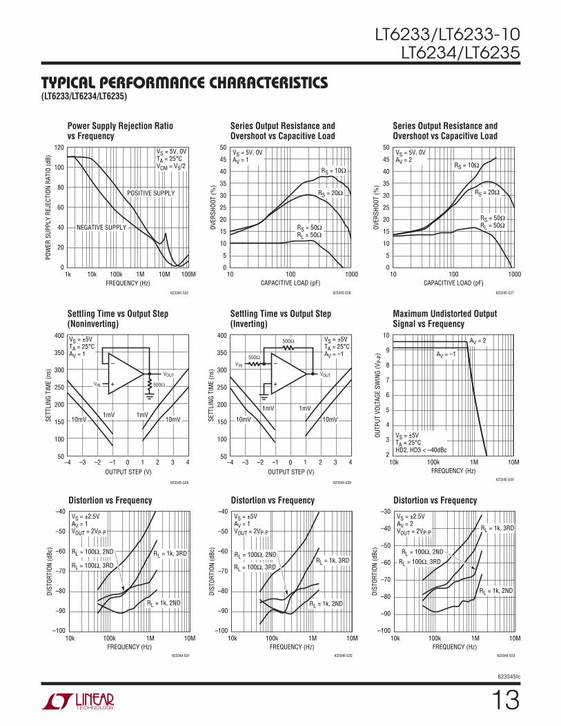
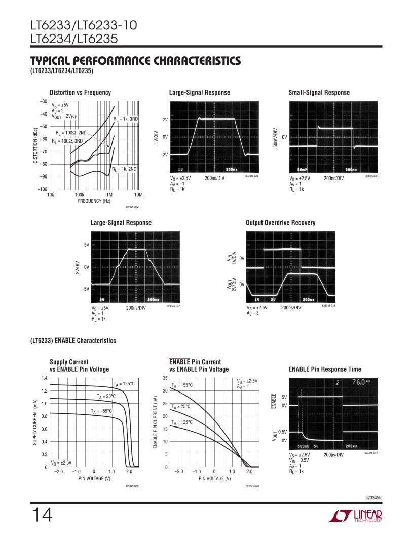
Typical perForMance characTerisTics
Input Bias Current vs Common Mode Voltage Input Bias Current vs Temperature
Output Saturation Voltage vs Load Current (Output Low)
VOS DistributionSupply Current vs Supply Voltage (Per Amplifier)
Offset Voltage vs Input Common Mode Voltage
(LT6233/LT6234/LT6235)
INPUT OFFSET VOLTAGE (µV)–2000
NUM
BER
OF U
NITS
10
20
30
40
–100 0 100 200
623345 GO1
50
60
–150 –50 50 150
VS = 5V, 0VVCM = V+/2S8
TOTAL SUPPLY VOLTAGE (V)0
SUPP
LY C
URRE
NT (m
A)
6
623345 GO2
2 4 8
2.0
1.5
1.0
0.5
010 12 14
TA = 125°C
TA = 25°C
TA = –55°C
INPUT COMMON MODE VOLTAGE (V)0OF
FSET
VOL
TAGE
(µV)
1.5
623345 GO3
0.5 1 2
500
400
300
200
100
0
–100
–200
–300
–400
–5003 4 52.5 3.5 4.5
TA = –55°C
TA = 25°C
TA = 125°C
VS = 5V, 0V
COMMON MODE VOLTAGE (V)–1
INPU
T BI
AS C
URRE
NT (µ
A)
2
623345 GO4
0 1 3
6
5
4
3
2
1
0
–2
–1
4 5 6
TA = 125°C
TA = –55°C
TA = 25°C
VS = 5V, 0V
TEMPERATURE (°C)–50
INPU
T BI
AS C
URRE
NT (µ
A)
25
623345 GO5
–25 0 50
6
5
4
3
2
1
0
–175 100 125
VCM = 4V
VCM = 1.5V
VS = 5V, 0V
LOAD CURRENT (mA) 0.01 0.10.0001
OUTP
UT S
ATUR
ATIO
N VO
LTAG
E (V
)
0.01
10
1 10010
623345 GO6
0.001
0.1
1
VS = 5V, 0V
TA = –55°C
TA = 125°C
TA = 25°C
11623345fc
LT6233/LT6233-10LT6234/LT6235
Typical perForMance characTerisTics
Open-Loop Gain Open-Loop Gain Open-Loop Gain
Offset Voltage vs Output Current Warm-Up Drift vs TimeTotal Noise vs Total Source Resistance
Output Saturation Voltage vs Load Current (Output High) Minimum Supply Voltage
Output Short-Circuit Current vs Power Supply Voltage
(LT6233/LT6234/LT6235)
LOAD CURRENT (mA)
OUTP
UT S
ATUR
ATIO
N VO
LTAG
E (V
)
623345 G07
0.01 0.1
0.01
10
1 100100.001
0.1
1
VS = 5V, 0V
TA = –55°C
TA = 125°C
TA = 25°C
TOTAL SUPPLY VOLTAGE (V)0
OFFS
ET V
OLTA
GE (m
V)
1.5
623345 G08
0.5 1 2
1.0
0.8
0.6
0.4
0.2
0
–0.2
–0.4
–0.6
–0.8
–1.03 4 52.5 3.5 4.5
TA = –55°C
TA = 125°C
TA = 25°C
VCM = VS/2
POWER SUPPLY VOLTAGE (±V)1.5
OUTP
UT S
HORT
-CIR
CUIT
CUR
RENT
(mA)
3.0
623345 GO9
2.0 2.5 3.5
80
60
40
20
0
–20
–40
–80
–60
4.0 4.5 5.0
TA = 125°C
TA = –55°C
TA = –55°C
TA = 25°C
SINKING
SOURCING
TA = 25°C
TA = 125°C
OUTPUT VOLTAGE (V)0
INPU
T VO
LTAG
E (m
V)
1.5
623345 G10
0.5 1.0 2.0
2.5
2.0
1.5
1.0
0.5
0
–0.5
–1.0
–1.5
–2.0
–2.53.02.5
RL = 100Ω
RL = 1k
VS = 3V, 0VTA = 25°C
OUTPUT VOLTAGE (V)0
INPU
T VO
LTAG
E (m
V)
1.5
623345 G11
0.5 1 2
0
3 4 52.5 3.5 4.5
RL = 100Ω
RL = 1k
VS = 5V, 0VTA = 25°C
2.5
2.0
1.5
1.0
0.5
–0.5
–1.0
–1.5
–2.0
–2.5
OUTPUT VOLTAGE (V)–5
INPU
T VO
LTAG
E (m
V)
–2
623345 G12
–4 –3 –1
0
1 3 50 2 4
RL = 100Ω
RL = 1k
VS = ±5VTA = 25°C
2.5
2.0
1.5
1.0
0.5
–0.5
–1.0
–1.5
–2.0
–2.5
OUTPUT CURRENT (mA)–90
OFFS
ET V
OLTA
GE (m
V)
623345 G13
–60 –30
2.0
1.5
1.0
0.5
0
–0.5
–1.0
–1.5
–2.00 30 9060
TA = –55°C
TA = 125°C
VS = ±5V
TA = 25°C
TIME AFTER POWER-UP (s)0
CHAN
GE IN
OFF
SET
VOLT
AGE
(µV)
20
623345 G14
10 30
40
35
30
25
20
15
10
040 50
TA = 25°C
VS = ±5V
VS = ±2.5V
VS = ±1.5V
TOTAL SOURCE RESISTANCE (Ω)
1
TOTA
L NO
ISE
(nV/
√Hz)
10
10 1k 10k 100k
623345 G15
0.1100
100VS = ±2.5VVCM = 0Vf = 100kHzUNBALANCEDSOURCERESISTORS
TOTAL NOISE
RESISTOR NOISE
AMPLIFIER NOISE VOLTAGE

LT6233/LT6233-10LT6234/LT6235
12623345fc
Typical perForMance characTerisTics
Open-Loop Gain vs FrequencyGain Bandwidth and Phase Margin vs Supply Voltage Slew Rate vs Temperature
Output Impedance vs FrequencyCommon Mode Rejection Ratio vs Frequency Channel Separation vs Frequency
Noise Voltage and Unbalanced Noise Current vs Frequency
0.1Hz to 10Hz Output Voltage Noise
Gain Bandwidth and Phase Margin vs Temperature
(LT6233/LT6234/LT6235)
FREQUENCY (Hz)
NOIS
E VO
LTAG
E (n
V/√H
z)
6
5
4
3
2
1
010 1k 10k 100k
623345 G16
100
VS = ±2.5VTA = 25°CVCM = 0V
NOISE VOLTAGE
NOISE CURRENT
UNBALANCED NOISE CURRENT (pA/√Hz)
6
5
4
3
2
1
05s/DIV
623345 G17
100nV
100n
V/DI
V
–100nV
VS = ±2.5V
TEMPERATURE (°C)–55
GAIN
BAN
DWID
TH (M
Hz)
5
623345 G18
–25 35
90
80
70
60
40
50
PHASE MARGIN (DEG)
70
60
50
40
65 95 125
VS = ±5V
VS = 3V, 0V
VS = ±5V
VS = 3V, 0V
PHASE MARGIN
GAIN BANDWIDTH
CL = 5pFRL = 1kVCM = VS/2
FREQUENCY (Hz)
GAIN
(dB)
80
70
50
30
0
–10
60
40
10
20
–20
PHASE (DEG)
120
100
60
20
–60
80
40
–20
–40
0
–80100k 10M 100M 1G
623345 G19
1M
CL = 5pFRL = 1kVCM = VS/2
PHASE
GAIN
VS = ±5VVS = 3V, 0V
VS = ±5VVS = 3V, 0V
TOTAL SUPPLY VOLTAGE (V)0
GAIN
BAN
DWID
TH (M
Hz)
6
623345 G20
2 4 8
70
60
50
30
40
PHASE MARGIN (DEG)
80
70
60
50
40
10 12 14
PHASE MARGIN
GAIN BANDWIDTH
TA = 25°CCL = 5pFRL = 1k
TEMPERATURE (°C)–55
SLEW
RAT
E (V
/µs)
5
623345 G21
–35 –15 45
20
22
24
26
18
16
14
10
12
8525 65 105 125
VS = ±5V FALLING
VS = ±2.5V RISING
AV = –1RF = RG = 1k
VS = ±2.5V FALLING
VS = ±5V RISING
FREQUENCY (Hz)
1OUTP
UT IM
PEDA
NCE
(Ω)
10
100k 10M 100M
623345 G22
0.11M
1k
100
VS = 5V, 0V
AV = 10
AV = 1
AV = 2
FREQUENCY (Hz)
20
COM
MON
MOD
E RE
JECT
ION
RATI
O (d
B)
40
60
80
120
100
10k 100M100k 1G10M
623345 G23
01M
VS = 5V, 0VVCM = VS/2
FREQUENCY (Hz)100k
CHAN
NEL
SEPA
RATI
ON (d
B)
–40
–50
–60
–70
–80
–90
–100
–110
–120
–130
–1401M 10M 100M
623345 G24
AV = 1TA = 25°CVS = ±5V
13623345fc
LT6233/LT6233-10LT6234/LT6235
Typical perForMance characTerisTics
Settling Time vs Output Step (Noninverting)
Settling Time vs Output Step (Inverting)
Maximum Undistorted Output Signal vs Frequency
Distortion vs Frequency Distortion vs Frequency Distortion vs Frequency
Power Supply Rejection Ratio vs Frequency
Series Output Resistance and Overshoot vs Capacitive Load
Series Output Resistance and Overshoot vs Capacitive Load
(LT6233/LT6234/LT6235)
FREQUENCY (Hz)
20
POW
ER S
UPPL
Y RE
JECT
ION
RATI
O (d
B)
40
60
80
120
100
1k 10k 100M100k 10M
623345 G25
01M
VS = 5V, 0VTA = 25°CVCM = VS/2
NEGATIVE SUPPLY
POSITIVE SUPPLY
CAPACITIVE LOAD (pF)10
OVER
SHOO
T (%
)
50
45
40
35
30
25
20
15
10
5
0100 1000
623345 G26
VS = 5V, 0VAV = 1
RS = 10Ω
RS = 20Ω
RS = 50ΩRL = 50Ω
CAPACITIVE LOAD (pF)10
OVER
SHOO
T (%
)
50
45
40
35
30
25
20
15
10
5
0100 1000
623345 G27
VS = 5V, 0VAV = 2
RS = 10Ω
RS = 20Ω
RS = 50ΩRL = 50Ω
OUTPUT STEP (V)–4
SETT
LING
TIM
E (n
s)
0
623345 G28
–3 –2 –1 1
300
400
350
250
200
150
50
100
2 3 4
1mV10mV
1mV10mV
VS = ±5VTA = 25°CAV = 1
+
–
500Ω
VOUT
VIN
OUTPUT STEP (V)–4
SETT
LING
TIM
E (n
s)
0
623345 G29
–3 –2 –1 1
300
400
350
250
200
150
50
100
2 3 4
1mV
10mV
1mV
10mV
VS = ±5VTA = 25°CAV = –1
+
–
500Ω
500Ω
VOUT
VIN
FREQUENCY (Hz)10k
OUTP
UT V
OLTA
GE S
WIN
G (V
P-P)
10
9
8
7
6
5
4
3
2100k 1M 10M
623345 G30
VS = ±5VTA = 25°CHD2, HD3 < –40dBc
AV = –1
AV = 2
FREQUENCY (Hz)10k
DIST
ORTI
ON (d
Bc)
–40
–50
–60
–70
–80
–90
–100100k 1M 10M
623345 G31
VS = ±2.5VAV = 1VOUT = 2VP-P
RL = 100Ω, 3RD
RL = 1k, 3RD
RL = 1k, 2ND
RL = 100Ω, 2ND
FREQUENCY (Hz)10k
DIST
ORTI
ON (d
Bc)
–40
–50
–60
–70
–80
–90
–100100k 1M 10M
623345 G32
VS = ±5VAV = 1VOUT = 2VP-P
RL = 100Ω, 3RDRL = 1k, 3RD
RL = 1k, 2ND
RL = 100Ω, 2ND
FREQUENCY (Hz)10k
DIST
ORTI
ON (d
Bc)
–30
–40
–50
–60
–70
–80
–90
–100100k 1M 10M
623345 G33
VS = ±2.5VAV = 2VOUT = 2VP-P
RL = 100Ω, 3RD
RL = 1k, 3RD
RL = 1k, 2ND
RL = 100Ω, 2ND
LT6233/LT6233-10LT6234/LT6235
14623345fc
Typical perForMance characTerisTics
Distortion vs Frequency Large-Signal Response Small-Signal Response
(LT6233/LT6234/LT6235)
Large-Signal Response Output Overdrive Recovery
(LT6233) ENABLE Characteristics
Supply Current vs ENABLE Pin Voltage
ENABLE Pin Current vs ENABLE Pin Voltage ENABLE Pin Response Time
FREQUENCY (Hz)10k
DIST
ORTI
ON (d
Bc)
–30
–40
–50
–60
–70
–80
–90
–100100k 1M 10M
623345 G34
VS = ±5VAV = 2VOUT = 2VP-P
RL = 100Ω, 3RD
RL = 1k, 3RD
RL = 1k, 2ND
RL = 100Ω, 2ND
2V
0V
–2V
200ns/DIV 623345 G35VS = ±2.5VAV = –1RL = 1k
1V/D
IV
0V
200ns/DIV 623345 G36VS = ±2.5VAV = 1RL = 1k
50m
V/DI
V
0V
5V
–5V
200ns/DIV 623345 G37VS = ±5VAV = 1RL = 1k
2V/D
IV
0V
0V
200ns/DIV 623345 G38VS = ±2.5VAV = 3
V IN
1V/D
IVV O
UT2V
/DIV
PIN VOLTAGE (V)
SUPP
LY C
URRE
NT (m
A)
–1.0
623345 G39
–2.0 0
1.4
1.2
1.0
0.8
0.6
0.4
0.2
01.0 2.0
TA = 125°C
VS = ±2.5V
TA = 25°C
TA = –55°C
PIN VOLTAGE (V)
ENAB
LE P
IN C
URRE
NT (µ
A)
623345 G40
35
30
25
20
15
10
5
0
TA = 125°C
VS = ±2.5VAV = 1
TA = 25°C
TA = –55°C
–1.0–2.0 0 1.0 2.0
0V
5V
0.5V
0V
200µs/DIV 623345 G41VS = ±2.5VVIN = 0.5VAV = 1RL = 1k
V OUT
ENAB
LE
15623345fc
LT6233/LT6233-10LT6234/LT6235
Typical perForMance characTerisTics
Open-Loop Gain and Phase vs Frequency
Gain Bandwidth and Phase Margin vs Supply Voltage Gain Bandwidth vs Resistor Load
Common Mode Rejection Ratio vs Frequency
Maximum Undistorted Output vs Frequency
2nd and 3rd Harmonic Distortion vs Frequency
Gain Bandwidth and Phase Margin vs Temperature Slew Rate vs Temperature
Series Output Resistor and Overshoot vs Capacitive Load
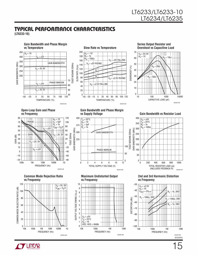
(LT6233-10)
TEMPERATURE (°C)–50
GAIN
BAN
DWID
TH (M
Hz)
25
623345 G42
–25 0 50
450
400
350
300
200
250
PHASE MARGIN (DEG)
70
60
50
4075 100 125
VS = ±5V
VS = 3V, 0V
VS = ±5V
VS = 3V, 0V
PHASE MARGIN
GAIN BANDWIDTH
AV = 10
TEMPERATURE (°C)–55
SLEW
RAT
E (V
/µs)
5
623345 G43
–35 –15 45
140
160
180
200
120
100
60
0
20
80
40
8525 65 105 125
VS = ±5V FALLING
VS = ±2.5V RISING
AV = –10RF = 1kRG = 100Ω
VS = ±2.5V FALLING
VS = ±5V RISING
CAPACITIVE LOAD (pF)10
OVER
SHOO
T (%
)
70
60
50
40
30
20
10
0100 1000 10000
623345 G44
VS = 5V, 0VAV = 10 RS = 10Ω
RS = 20Ω
RS = 50Ω
FREQUENCY (Hz)
GAIN
(dB)
80
70
60
50
40
30
20
10
0
–10
–20
PHASE (DEG)
120
100
80
60
40
20
0
–20
–40
–60
–80100k 10M 100M 1G
623345 G45
1M
AV = 10CL = 5pFRL = 1kVCM = VS/2
VS = 3V, 0V
VS = ±5V
PHASE
GAIN
VS = ±5V
VS = 3V, 0V
TOTAL SUPPLY VOLTAGE (V)0
GAIN
BAN
DWID
TH (M
Hz)
6
623345 G46
2 4 8
450
375
300
225
PHASE MARGIN (DEG)
100
50
010 12
PHASE MARGIN
GAIN BANDWIDTH
TA = 25°CAV = 10CL = 5pFRL = 1k
TOTAL RESISTOR LOAD (Ω)(INCLUDES FEEDBACK R)
0
GAIN
BAN
DWID
TH (M
Hz)
600
623345 G47
200 400 800
400
350
300
200
150
100
50
0
250
1000
AV = 10VS = ±5VTA = 25°CRF = 1kRG = 100Ω
FREQUENCY (Hz)
20
COM
MON
MOD
E RE
JECT
ION
RATI
O (d
B)
40
60
80
120
100
10k 1G100M100k 10M
623345 G48
01M
VS = 5V, 0VVCM = VS/2
FREQUENCY (Hz)10k
OUTP
UT V
OLTA
GE S
WIN
G (V
P-P)
10
9
8
7
6
5
4
3
2
1
0100k 1M 10M
623345 G49
VS = ±5VTA = 25°CAV = 10HD2, HD3 ≤ 40dBc
FREQUENCY (Hz)10k
DIST
ORTI
ON (d
Bc)
–30
–40
–50
–60
–70
–80
–90
–100100k 1M 10M
623345 G50
VS = ±2.5VAV = 10VOUT = 2VP-P
RL = 100Ω, 3RDRL = 100Ω, 2ND
RL = 1k, 3RD
RL = 1k, 2ND
LT6233/LT6233-10LT6234/LT6235
16623345fc
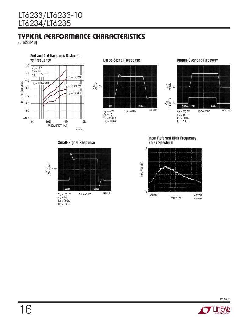
Typical perForMance characTerisTics
2nd and 3rd Harmonic Distortion vs Frequency Large-Signal Response Output-Overload Recovery
(LT6233-10)
Small-Signal ResponseInput Referred High Frequency Noise Spectrum
FREQUENCY (Hz)10k
DIST
ORTI
ON (d
Bc)
–30
–40
–50
–60
–70
–80
–90
–100100k 1M 10M
623345 G51
VS = ±5VAV = 10VOUT = 2VP-P
RL = 100Ω, 3RDRL = 100Ω, 2ND
RL = 1k, 3RD
RL = 1k, 2ND
0V
100ns/DIV 623345 G52VS = ±5VAV = 10RF = 900ΩRG = 100Ω
V OUT
2V/D
IV
0V
100ns/DIV 623345 G53VS = 5V, 0VAV = 10RF = 900ΩRG = 100Ω
V OUT
2V/D
IV
0VV IN
0.5V
/DIV
2.5V
100ns/DIV 623345 G54VS = 5V, 0VAV = 10RF = 900ΩRG = 100Ω
V OUT
100m
V/DI
V
10
0
2MHz/DIV 623345 G55
100kHz 20MHz
1nV/
√Hz/
DIV

17623345fc
LT6233/LT6233-10LT6234/LT6235
applicaTions inForMaTion
Figure 1. Simplified Schematic
Figure 2. VS = ±2.5V, AV = 1 with Large Overdrive
ENABLE
DESD6
DESD5
–V
+V
+VIN
–VIN+V
623345 F01
BIAS
DIFFERENTIALDRIVE GENERATOR
VOUT
+V
CM
I1
–V
DESD3
–V
–V
DESD4
+V
DESD1
–V
DESD2
+V
D1
C1
D2
Q5
Q6
Q4
Q2
Q3
Q1
2.5V
–2.5V
0V
500µs/DIV 623345 F02
1V/D
IV
Amplifier Characteristics
Figure 1 is a simplified schematic of the LT6233/LT6234/LT6235, which has a pair of low noise input transistors Q1 and Q2. A simple current mirror Q3/Q4 converts the differential signal to a single-ended output, and these transistors are degenerated to reduce their contribution to the overall noise.
Capacitor C1 reduces the unity-cross frequency and im-proves the frequency stability without degrading the gain bandwidth of the amplifier. Capacitor CM sets the overall amplifier gain bandwidth. The differential drive generator supplies current to transistors Q5 and Q6 that swing the output from rail-to-rail.
Input Protection
There are back-to-back diodes, D1 and D2 across the + and – inputs of these amplifiers to limit the differential input voltage to ±0.7V. The inputs of the LT6233/LT6234/LT6235 do not have internal resistors in series with the input tran-sistors. This technique is often used to protect the input devices from overvoltage that causes excessive current to flow. The addition of these resistors would significantly degrade the low noise voltage of these amplifiers. For instance, a 100Ω resistor in series with each input would generate 1.8nV/√Hz of noise, and the total amplifier noise voltage would rise from 1.9nV/√Hz to 2.6nV/√Hz. Once the input differential voltage exceeds ±0.7V, steady-state current conducted through the protection diodes should
be limited to ±40mA. This implies 25Ω of protection re-sistance is necessary per volt of overdrive beyond ±0.7V. These input diodes are rugged enough to handle transient currents due to amplifier slew rate overdrive and clipping without protection resistors.
The photo of Figure 2 shows the output response to an input overdrive with the amplifier connected as a voltage follower. With the input signal low, current source I1 satu-rates and the differential drive generator drives Q6 into saturation so the output voltage swings all the way to V–. The input can swing positive until transistor Q2 saturates into current mirror Q3/Q4. When saturation occurs, the output tries to phase invert, but diode D2 conducts current from the signal source to the output through the feedback connection. The output is clamped a diode drop below the input. In this photo, the input signal generator is limiting at about 20mA.
LT6233/LT6233-10LT6234/LT6235
18623345fc
applicaTions inForMaTionWith the amplifier connected in a gain of AV ≥ 2, the output can invert with very heavy overdrive. To avoid this inver-sion, limit the input overdrive to 0.5V beyond the power supply rails.
ESD
The LT6233/LT6234/LT6235 have reverse-biased ESD protection diodes on all inputs and outputs as shown in Figure 1. If these pins are forced beyond either supply, unlimited current will flow through these diodes. If the current is transient and limited to one hundred milliamps or less, no damage to the device will occur.
Noise
The noise voltage of the LT6233/LT6234/LT6235 is equivalent to that of a 225Ω resistor, and for the lowest possible noise it is desirable to keep the source and feed-back resistance at or below this value, i.e., RS + RG||RFB ≤ 225Ω. With RS + RG||RFB = 225Ω the total noise of the amplifier is:
eN = √(1.9nV)2 + (1.9nV)2 = 2.69nV/√Hz
Below this resistance value, the amplifier dominates the noise, but in the region between 225Ω and about 30k, the noise is dominated by the resistor thermal noise. As the total resistance is further increased beyond 30k, the amplifier noise current multiplied by the total resistance eventually dominates the noise.
The product of eN • √ISUPPLY is an interesting way to gauge low noise amplifiers. Most low noise amplifiers with low eN have high ISUPPLY current. In applications that require low noise voltage with the lowest possible supply current, this product can prove to be enlightening. The LT6233/LT6234/LT6235 have an eN • √ISUPPLY product of only 2.1 per amplifier, yet it is common to see amplifiers with similar noise specifications to have eN • √ISUPPLY as high as 13.5.
For a complete discussion of amplifier noise, see the LT1028 data sheet.
Enable Pin
The LT6233 and LT6233-10 include an ENABLE pin that shuts down the amplifier to 10µA maximum supply cur-rent. The ENABLE pin must be driven low to operate the amplifier with normal supply current. The ENABLE pin must be driven high to within 0.35V of V+ to shut down the supply current. This can be accomplished with simple gate logic; however care must be taken if the logic and the LT6233 operate from different supplies. If this is the case, then open-drain logic can be used with a pull-up resis-tor to ensure that the amplifier remains off. See Typical Performance Characteristics.
The output leakage current when disabled is very low; however, current can flow into the input protection diodes D1 and D2 if the output voltage exceeds the input voltage by a diode drop.
19623345fc
LT6233/LT6233-10LT6234/LT6235
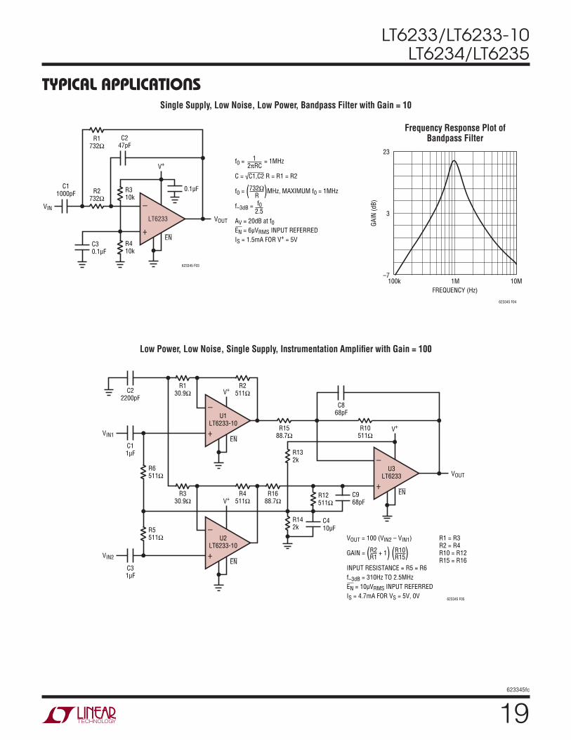
Typical applicaTionsSingle Supply, Low Noise, Low Power, Bandpass Filter with Gain = 10
Frequency Response Plot of Bandpass Filter
Low Power, Low Noise, Single Supply, Instrumentation Amplifier with Gain = 100
R2732Ω
R410k
C30.1µF
EN
f0 = 1 = 1MHz
C = √C1,C2 R = R1 = R2
f0 = (732Ω)MHz, MAXIMUM f0 = 1MHz
f–3dB = f0
AV = 20dB at f0EN = 6µVRMS INPUT REFERREDIS = 1.5mA FOR V+ = 5V
623345 F03
0.1µF
C247pF
C11000pF R3
10k
R1732Ω
VOUT
V+
VIN
2πRC
R
2.5
+
–LT6233
FREQUENCY (Hz)100k
GAIN
(dB)
23
3
–71M 10M
623345 F04
+
–
R142k
EN
U3LT6233
VOUT = 100 (VIN2 – VIN1)
GAIN = (R2 + 1) (R10)INPUT RESISTANCE = R5 = R6f–3dB = 310Hz TO 2.5MHzEN = 10µVRMS INPUT REFERREDIS = 4.7mA FOR VS = 5V, 0V 623345 F05
C868pF
C31µF
R132k
R10511Ω
R1588.7Ω
R1688.7Ω
R4511Ω
R330.9Ω
R130.9Ω
R2511Ω
VOUT
VIN1
VIN2
V+
R1 R15
C968pF
R12511Ω
+
–
EN
U2LT6233-10
V+
C11µF
C22200pF
+
–
EN
U1LT6233-10
V+
R5511Ω
R6511Ω
C410µF
R1 = R3R2 = R4R10 = R12R15 = R16
LT6233/LT6233-10LT6234/LT6235
20623345fc
package DescripTionS6 Package
6-Lead Plastic TSOT-23(Reference LTC DWG # 05-08-1636)
1.50 – 1.75(NOTE 4)
2.80 BSC
0.30 – 0.45 6 PLCS (NOTE 3)
DATUM ‘A’
0.09 – 0.20(NOTE 3) S6 TSOT-23 0302
2.90 BSC(NOTE 4)
0.95 BSC
1.90 BSC
0.80 – 0.90
1.00 MAX0.01 – 0.10
0.20 BSC
0.30 – 0.50 REF
PIN ONE ID
NOTE:1. DIMENSIONS ARE IN MILLIMETERS2. DRAWING NOT TO SCALE3. DIMENSIONS ARE INCLUSIVE OF PLATING4. DIMENSIONS ARE EXCLUSIVE OF MOLD FLASH AND METAL BURR5. MOLD FLASH SHALL NOT EXCEED 0.254mm6. JEDEC PACKAGE REFERENCE IS MO-193
3.85 MAX
0.62MAX
0.95REF
RECOMMENDED SOLDER PAD LAYOUTPER IPC CALCULATOR
1.4 MIN2.62 REF
1.22 REF

21623345fc
LT6233/LT6233-10LT6234/LT6235
package DescripTionDD Package
8-Lead Plastic DFN (3mm × 3mm)(Reference LTC DWG # 05-08-1698 Rev C)
3.00 ±0.10(4 SIDES)
NOTE:1. DRAWING TO BE MADE A JEDEC PACKAGE OUTLINE M0-229 VARIATION OF (WEED-1)2. DRAWING NOT TO SCALE3. ALL DIMENSIONS ARE IN MILLIMETERS4. DIMENSIONS OF EXPOSED PAD ON BOTTOM OF PACKAGE DO NOT INCLUDE MOLD FLASH. MOLD FLASH, IF PRESENT, SHALL NOT EXCEED 0.15mm ON ANY SIDE5. EXPOSED PAD SHALL BE SOLDER PLATED6. SHADED AREA IS ONLY A REFERENCE FOR PIN 1 LOCATION ON TOP AND BOTTOM OF PACKAGE
0.40 ± 0.10
BOTTOM VIEW—EXPOSED PAD
1.65 ± 0.10(2 SIDES)
0.75 ±0.05
R = 0.125TYP
2.38 ±0.10
14
85
PIN 1TOP MARK
(NOTE 6)
0.200 REF
0.00 – 0.05
(DD8) DFN 0509 REV C
0.25 ± 0.05
2.38 ±0.05
RECOMMENDED SOLDER PAD PITCH AND DIMENSIONSAPPLY SOLDER MASK TO AREAS THAT ARE NOT SOLDERED
1.65 ±0.05(2 SIDES)2.10 ±0.05
0.50BSC
0.70 ±0.05
3.5 ±0.05
PACKAGEOUTLINE
0.25 ± 0.050.50 BSC
LT6233/LT6233-10LT6234/LT6235
22623345fc
package DescripTionS8 Package
8-Lead Plastic Small Outline (Narrow .150 Inch)(Reference LTC DWG # 05-08-1610)
.016 – .050(0.406 – 1.270)
.010 – .020(0.254 – 0.508)
× 45°
0°– 8° TYP.008 – .010
(0.203 – 0.254)
SO8 0303
.053 – .069(1.346 – 1.752)
.014 – .019(0.355 – 0.483)
TYP
.004 – .010(0.101 – 0.254)
.050(1.270)
BSC
1 2 3 4
.150 – .157(3.810 – 3.988)
NOTE 3
8 7 6 5
.189 – .197(4.801 – 5.004)
NOTE 3
.228 – .244(5.791 – 6.197)
.245MIN .160 ±.005
RECOMMENDED SOLDER PAD LAYOUT
.045 ±.005 .050 BSC
.030 ±.005 TYP
INCHES(MILLIMETERS)
NOTE:1. DIMENSIONS IN
2. DRAWING NOT TO SCALE3. THESE DIMENSIONS DO NOT INCLUDE MOLD FLASH OR PROTRUSIONS. MOLD FLASH OR PROTRUSIONS SHALL NOT EXCEED .006" (0.15mm)
GN Package16-Lead Plastic SSOP (Narrow .150 Inch)
(Reference LTC DWG # 05-08-1641)
GN16 (SSOP) 0204
1 2 3 4 5 6 7 8
.229 – .244(5.817 – 6.198)
.150 – .157**(3.810 – 3.988)
16 15 14 13
.189 – .196*(4.801 – 4.978)
12 11 10 9
.016 – .050(0.406 – 1.270)
.015 ± .004(0.38 ± 0.10)
× 45°
0° – 8° TYP.007 – .0098(0.178 – 0.249)
.0532 – .0688(1.35 – 1.75)
.008 – .012(0.203 – 0.305)
TYP
.004 – .0098(0.102 – 0.249)
.0250(0.635)
BSC
.009(0.229)
REF
.254 MIN
RECOMMENDED SOLDER PAD LAYOUT
.150 – .165
.0250 BSC.0165 ±.0015
.045 ±.005
* DIMENSION DOES NOT INCLUDE MOLD FLASH. MOLD FLASH SHALL NOT EXCEED 0.006" (0.152mm) PER SIDE** DIMENSION DOES NOT INCLUDE INTERLEAD FLASH. INTERLEAD FLASH SHALL NOT EXCEED 0.010" (0.254mm) PER SIDE
INCHES(MILLIMETERS)
NOTE:1. CONTROLLING DIMENSION: INCHES
2. DIMENSIONS ARE IN
3. DRAWING NOT TO SCALE

23623345fc
LT6233/LT6233-10LT6234/LT6235
Information furnished by Linear Technology Corporation is believed to be accurate and reliable. However, no responsibility is assumed for its use. Linear Technology Corporation makes no representa-tion that the interconnection of its circuits as described herein will not infringe on existing patent rights.
revision hisToryREV DATE DESCRIPTION PAGE NUMBER
C 1/11 Revised y-axis lable on curve G40 in Typical Performance CharacteristicsUpdated ENABLE Pin section in Applications Information
1418
(Revision history begins at Rev C)
LT6233/LT6233-10LT6234/LT6235
24623345fc
Linear Technology Corporation1630 McCarthy Blvd., Milpitas, CA 95035-7417 (408) 432-1900 ● FAX: (408) 434-0507 ● www.linear.com LINEAR TECHNOLOGY CORPORATION 2003
LT 0111 REV C • PRINTED IN USA
relaTeD parTs
Typical applicaTions
Low Power Avalanche Photodiode Transimpedance Amplifier IS = 1.2mA
Photodiode Amplifier Time Domain Response
PART NUMBER DESCRIPTION COMMENTS
LT1028 Single, Ultralow Noise 50MHz Op Amp 0.85nV/√Hz
LT1677 Single, Low Noise Rail-to-Rail Amplifier 3V Operation, 2.5mA, 4.5nV/√Hz, 60µV Max VOS
LT1806/LT1807 Single/Dual, Low Noise 325MHz Rail-to-Rail Amplifier 2.5V Operation, 550µV Max VOS, 3.5nV/√Hz
LT6200/LT6201 Single/Dual, Low Noise 165MHz 0.95nV√Hz, Rail-to-Rail Input and Output
LT6202/LT6203/LT6204 Single/Dual/Quad, Low Noise, Rail-to-Rail Amplifier 1.9nV/√Hz, 3mA Max, 100MHz Gain Bandwidth
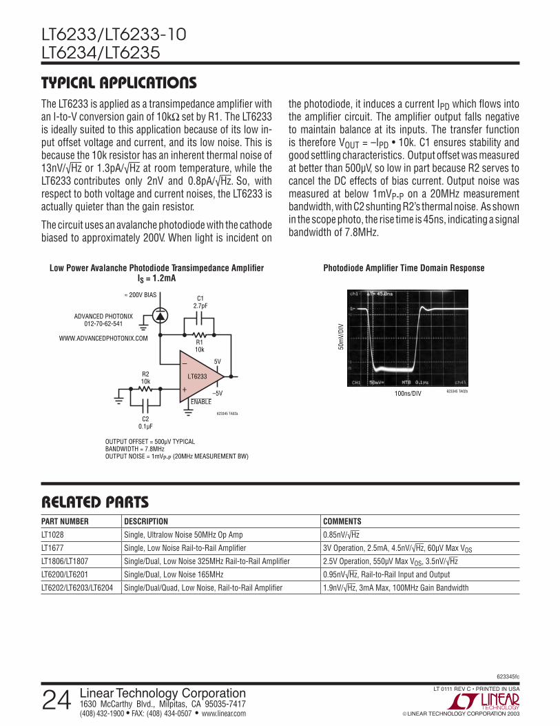
The LT6233 is applied as a transimpedance amplifier with an I-to-V conversion gain of 10kΩ set by R1. The LT6233 is ideally suited to this application because of its low in-put offset voltage and current, and its low noise. This is because the 10k resistor has an inherent thermal noise of 13nV/√Hz or 1.3pA/√Hz at room temperature, while the LT6233 contributes only 2nV and 0.8pA/√Hz. So, with respect to both voltage and current noises, the LT6233 is actually quieter than the gain resistor.
The circuit uses an avalanche photodiode with the cathode biased to approximately 200V. When light is incident on
the photodiode, it induces a current IPD which flows into the amplifier circuit. The amplifier output falls negative to maintain balance at its inputs. The transfer function is therefore VOUT = –IPD • 10k. C1 ensures stability and good settling characteristics. Output offset was measured at better than 500µV, so low in part because R2 serves to cancel the DC effects of bias current. Output noise was measured at below 1mVP-P on a 20MHz measurement bandwidth, with C2 shunting R2’s thermal noise. As shown in the scope photo, the rise time is 45ns, indicating a signal bandwidth of 7.8MHz.
+
–
R110k
R210k
C20.1µF
5V
–5VENABLE
LT6233
≈ 200V BIAS
ADVANCED PHOTONIX012-70-62-541
WWW.ADVANCEDPHOTONIX.COM
OUTPUT OFFSET = 500µV TYPICALBANDWIDTH = 7.8MHzOUTPUT NOISE = 1mVP-P (20MHz MEASUREMENT BW)
623345 TA02a
C12.7pF
100ns/DIV 623345 TA02b
50m
V/DI
V