6204.design considerations for ecg systems
DESCRIPTION
DESIGN CONSIDERATIONS FOR ECG SYSTEMSTRANSCRIPT
1

2

3

4
Biopotentials are developed from electrochemical gradients established across cell
membranes. These are voltage differences that exist between separated points in
living cells, tissues, and organelles. The potential difference measured with
electrodes between a living cell’s interior cytoplasm and the exterior aqueous
medium is generally called the membrane potential or resting potential (ERP). This
potential is relatively constant in striated muscle cells with a potential of about -50
to -100mV. Nerve cells show a similar range2.
Related to these biopotentials are the ionic charge transfers, or currents that give
rise to much of the electrical changes occurring in nerve, muscles and other
electrically active cells3. This current is the direct result of the electrochemistry
associated with ions internal and external to the cell.
The biopotential plot has a rising section depicting depolarization and a falling
section indicating repolarization. Depolarization can simply be though of as the
electrical stimulation of the heart muscle cells. During depolarization the muscle
fibers shorten causing contraction. While during repolarization the muscle cells
relax, lengthen, and return to the resting state4.
2,3 Biopotentials and Ionic currents, “Answers.com”
4 Welch Allyn Protocol Clinical Support

5

6

7

8
The ECG pulse is initiated by the body’s natural pace maker referred to as the
sinoatrial node (SA node). This initiates a wave of depolarization that starts with
the atrial muscle to the AV node, to the common bundle, to the bundle branches,
to the purkinje fibers, and finally to the ventricles. Because each portion of the
heart has a unique contribution to the composite ECG waveform, arrythmias can
be targeted to a very specific malfunction in the heart by dissecting the ECG
waveform itself.

9

10
11

12

13

14
A “lead” is not the same as an electrode contact, it is actually the difference
between 2 limb potentials. As an example LEAD I configuration is the difference
between the LA and RA with respect to the common mode reference.
The ECG Einthoven triangle dates back to the earliest days of electrocardiography
and provides the basis for electrode placement. The equilateral triangle is formed
by raising the arms and positioning the points on the limbs equidistant. Either leg
may be used for a lead connection and the other leg then becomes the reference
to which the other limbs are referenced, although the RL has conventionally
become the standard common mode reference.
The lead vectors associated with Einthoven’s lead system are conventionally
found based on the assumption that the heart is located at the center of a infinite,
homogenous volume conductor (at the center of a homogeneous sphere
representing the torso). With these assumptions, the voltages measured by the
three limb leads are proportional to the projections of the electric heart vector on
the sides of the lead vector triangle7. Einthoven’s Law provides the voltage
relationships between the leads.
With time this was perfected into the more commonly used connections today,
which may include as many as 12 electrodes. This allows the heart biopotential
activity to be monitored through many different planes.
7 buttler.cc.tut.fi

15
The Eintoven Triangle does not yields Lead I, II, and III but it also gives the ability
to calculate or derive a reference potential for the chest leads. This can be done
in software by taking the average voltage of the RA, LA, and LL, or it can be done
in hardware by summing the potentials at each limb through 3 equal-valued
resistors. This summed voltage is referred to as the “Wilson Central.”

16
This slide uses Mr. Bill to show how a simplified look at how the Wilson Central
becomes the negative input to a differential sensing amplifier with respect to the
different chest lead positions.
17
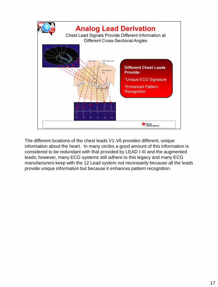
The different locations of the chest leads V1-V6 provides different, unique
information about the heart. In many circles a good amount of this information is
considered to be redundant with that provided by LEAD I-III and the augmented
leads; however, many ECG systems still adhere to this legacy and many ECG
manufacturers keep with the 12 Lead system not necessarily because all the leads
provide unique information but because it enhances pattern recognition.

18
Pattern recognition is further enhanced by the Golderberger terminal or the
Augmented Leads (AVL, AVR, AVF). Golderberger observed that he could obtain a
50% larger signal than using the Wilson Central as the reference.

19
The overall reason for all of these different leads is that it gives the physician
different angles from which to observe the ECG waveform. From a diagnostic
standpoint this gives the physician more versatility and a better picture of
arrythmias when they occur.

20
This is a summary of the standard leads and configurations

21

22
ECG circuitry has to work in tandem with a defibrillation machine. Defibrillation is
the act of apply a large stimulus voltage to the heart when ventricular fibrillation
occurs in a patient. Ventricular fibrillation is the point which the left ventrical is
fluttering out of control and doing nothing to pump blood throughout the body.
This is often characterized by the “flatline.”
(1) Ne2H lamps—Become low impedance when a high voltage pulse is applied;
clamps the voltage @ 25-80V.
(2) A minimum of 100k ohms of series input resistance is required in ECG system
to protect the patient and the electrical circuitry from over current conditions.
Oftentimes this is broken up into 2 separate resistors so additional low pass
filtering can be used to get rid of external EMI/RFI. The differential capacitor is
always chosen across the inputs to be 10x the CCM capacitor because it will
break a decade before the common mode capacitor and keep common mode
RC mismatch from becoming differential noise to the input amplifier.
(3) The protection diodes can be signal or Zener diodes and clamp the voltage to a
range that is with in the SOA of the linear device (INA, OPA, PGA).
(4) The Zener Diodes provide a low impedance path for current to flow in the event
that the supplies are not established and there is a current that is injected into
the front of the INA from an external input stimulus. This along with the ESD
diodes of the device steers current away from the internal circuitry and into
ground.

23
This is a TINA spice simulation circuit for the response of the protection circuitry to
a defibrillation pulse. The input voltage source, Vpulse represents the
Defibrillation voltage pads and the ECGp and ECGn sources represent to
differential components of the ECG signal that go to each input of the INA.

24
Note that each component of the Defibrillation protection circuitry performs its task
well.
(1) Defibrillation voltage is clamped to +/-40V at Vclamp1 and Vclamp2
(2) Input current is limited to < 500uA into the INA. This meets the electrical
requirements of < 10mA to prevent damage to the device
(3) Assuming Vout is on a 5V process such as TI’s HPA07, the voltage at the
inputs is clamped by the signal diodes to < 7V which meets the SOA
requirements of the process
25
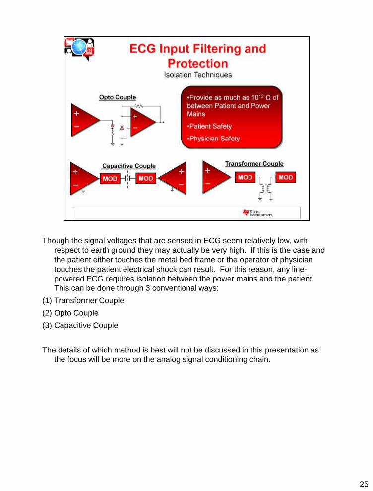
Though the signal voltages that are sensed in ECG seem relatively low, with
respect to earth ground they may actually be very high. If this is the case and
the patient either touches the metal bed frame or the operator of physician
touches the patient electrical shock can result. For this reason, any line-
powered ECG requires isolation between the power mains and the patient.
This can be done through 3 conventional ways:
(1) Transformer Couple
(2) Opto Couple
(3) Capacitive Couple
The details of which method is best will not be discussed in this presentation as
the focus will be more on the analog signal conditioning chain.

26
27
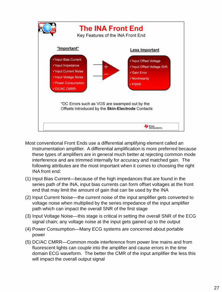
Most conventional Front Ends use a differential amplifying element called an
Instrumentation amplifier. A differential amplification is more preferred because
these types of amplifiers are in general much better at rejecting common mode
interference and are trimmed internally for accuracy and matched gain. The
following attributes are the most important when it comes to choosing the right
INA front end:
(1) Input Bias Current—because of the high impedances that are found in the
series path of the INA, input bias currents can form offset voltages at the front
end that may limit the amount of gain that can be used by the INA
(2) Input Current Noise—the current noise of the input amplifier gets converted to
voltage noise when multiplied by the series impedance of the input amplifier
path which can impact the overall SNR of the first stage
(3) Input Voltage Noise—this stage is critical in setting the overall SNR of the ECG
signal chain; any voltage noise at the input gets gained up to the output
(4) Power Consumption—Many ECG systems are concerned about portable
power
(5) DC/AC CMRR—Common mode interference from power line mains and from
fluorescent lights can couple into the amplifier and cause errors in the time
domain ECG waveform. The better the CMR of the input amplifier the less this
will impact the overall output signal

28
This simulation circuit is a simple demonstration of the ECG output waveforms
when connected to an electrode-patient impedance model and the front low pass
filtering on the INA. The INA in this case uses an Ideal source in TINA.

29
This is a simulation circuit that will show the impact of current noise and voltage
noise vs. gain at the output of the ECG waveform. The 1/f and broadband noise of
the noise source can be adjusted by double-clicking on the TINA symbol and
adjusting inside the text macromodel. This sources are very useful for building an
accurate noise model of amplifiers, especially if the performance of a TI amplifier
is needed to be compared against a competitor.

30
This plot shows how noise appears at the output linearly with respect to gain. The
ECG signal will vary linearly with the gain, so it is important in this stage to reduce
noise as much as possible, i.e. choose an amplifier that has the lowest noise for a
given power budget.
31
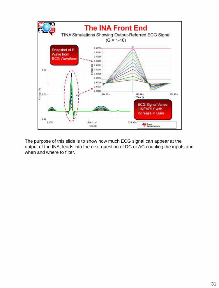
The purpose of this slide is to show how much ECG signal can appear at the
output of the INA; leads into the next question of DC or AC coupling the inputs and
when and where to filter.

32
The Feedback Integrator is a high pass filter that removes all of the offsets
incurred from the electrodes, offsets, offset drift, etc; however, it works by
adjusting the output of the integrator (3) in response to the instantaneous level of
the output of the INA. If the gained up output to the INA produces a difference
greater than Vref (assuming Vref is centered mid supply) the output of the
integrator will saturate into either the positive rail or ground and its ability to
remove DC will be eliminated. Consequently, the output of the INA will pull away
from Vref proportional to the difference between Vref.
Therefore, even though most ECG signals are in the mV range, since the
electrode offsets can be as much as +/-300mV, it is really not possible to use more
than a gain of 5-6 on the front end INA without risking possible saturation with the
degradation of electrode contacts.

33
This is a simulation circuit which demonstrates this principle using an ideal INA
TINA source and an OPA333. In the following slide you will see a plot of the
output, Vout, and how it maintains its DC value at Vref until the correction voltage
for the integrator exceeds Vref in magnitude.

34
This plot shows how after a gain = 6 the INA output can no longer track Vref
because the OPA333 integrator is saturated.

35
We’ve determined that the first stage of the ECG amplifier, like any sensor stage is
critical. So why not AC couple? AC coupling would remove the DC electrode
offsets and any other offsets incurred from IB*R and would allow a gain of 100 to
be used! We would not need any post gain stages nor complex filtering.

36
In this simulation circuit the ideal INA gain block is swept while the common mode
voltage is held at a constant Vref = 2.5V.
37
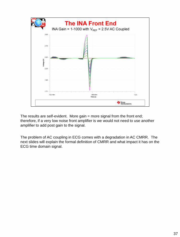
The results are self-evident. More gain = more signal from the front end;
therefore, if a very low noise front amplifier is we would not need to use another
amplifier to add post gain to the signal.
The problem of AC coupling in ECG comes with a degradation in AC CMRR. The
next slides will explain the formal definition of CMRR and what impact it has on the
ECG time domain signal.

38
The Inputs to a Differential Amplifying Element is composed of both a differential
and what is referred to as a “common mode” component. The differential signal is
the primary acquisition signal of interest and the common mode signal is the
component that is undesired. It is a necessary component because it is where the
differential signal rides and it is often there to keep the amplifier in linear operation.
Because amplifiers are not ideal when the common mode component VCM
changes there will also be a corresponding change in internal offset voltage. The
amount that this offset changes is directly proportional to the CMRR, or common
mode rejection ratio. This is the amplifier’s ability to reject a common mode signal
from becoming differential and amplifying itself to the output.
The equation shown on this slide shows how the magnitude of the amplifier’s
CMRR can impact its change in VOS.

39
When you AC couple the inputs it is always necessary to pull the inputs up to a DC
voltage such as Vref to ensure that there is an input bias current return path and
that the INA is in a linear region of operation. If there is mismatch in the RC of
each leg this mismatch will create a differential error that will be amplified to the
output. How much signal gets amplified to the output is dependent on the
frequency and the amount of mismatch between R and C in each leg.

40
This simulation circuit takes one of the input coupling capacitors and uses it as a
controlled object under the “analysis” tab and the frequency is swept with VCM
connected as shown.
41
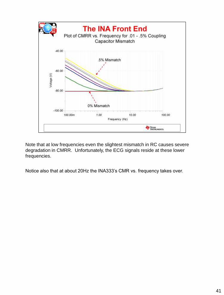
Note that at low frequencies even the slightest mismatch in RC causes severe
degradation in CMRR. Unfortunately, the ECG signals reside at these lower
frequencies.
Notice also that at about 20Hz the INA333’s CMR vs. frequency takes over.

42
As can be seen by this time domain plot, any slow-moving common mode artifacts
will couple directly in to the ECG signal if there is a slight mismatch in the coupling
capacitors in an AC-coupled system. It is for this reason that many prefer to DC
couple the front end and then post gain and filter.
Ultimately the question of whether or not to AC couple boils down to whether the
application will be susceptible to low frequency changes in common mode voltage.
If this is the case, AC coupling is probably not the best way to go; however, if the
ECG designer is confident that the only low frequency signals that will exist will be
the ECG signals themselves and are not worried about the impact of change of
DC common mode changes, perhaps AC coupling is an acceptable route to take.

43
Even in the DC coupled case the common mode rejection of the INA is often not
good enough to get rid of common mode noise from the power lines. The next
couple of slides will cover some ways to reduce the impact of common mode noise
on ECG systems.
This plot shows the how 50/60Hz will couple into the INA regardless of whether the
system is AC or DC coupled. At this frequency the RC mismatch on the front end
becomes a non-issue and the CMRR of the INA takes over.

44

45
It is possible to amplify an ECG signal and create a DC common mode bias
electrically off the inputs of the INA; however, in doing this there is extreme
susceptibility to common mode interference which is where the need for the RL
drive comes in. The RL drive is biased at a potential (usually Vs/2) and it inverts
and amplifies the average common mode signal back into the patient’s right leg.
This action cancels 50/60Hz noise and creates a more clean ECG output signal.
The more gain that can be used in the feedback loop the better in terms of
improving CMR. Canceling noise in this way relaxes the attenuation needed from
the CMR of the INA.
The gain that can be used in the feedback of the RL drive is limited by the
electrode offset and the offset of the amplifier as well as the supply rail. A
saturated RL drive amplifier is worthless, so putting too much gain in the loop is
not a good idea.
The other consideration that must be made is the stability of the RL drive amplifier
because the body contact impedance, and the INA serve as a large feedback loop
that can become unstable if not compensated correctly.
46
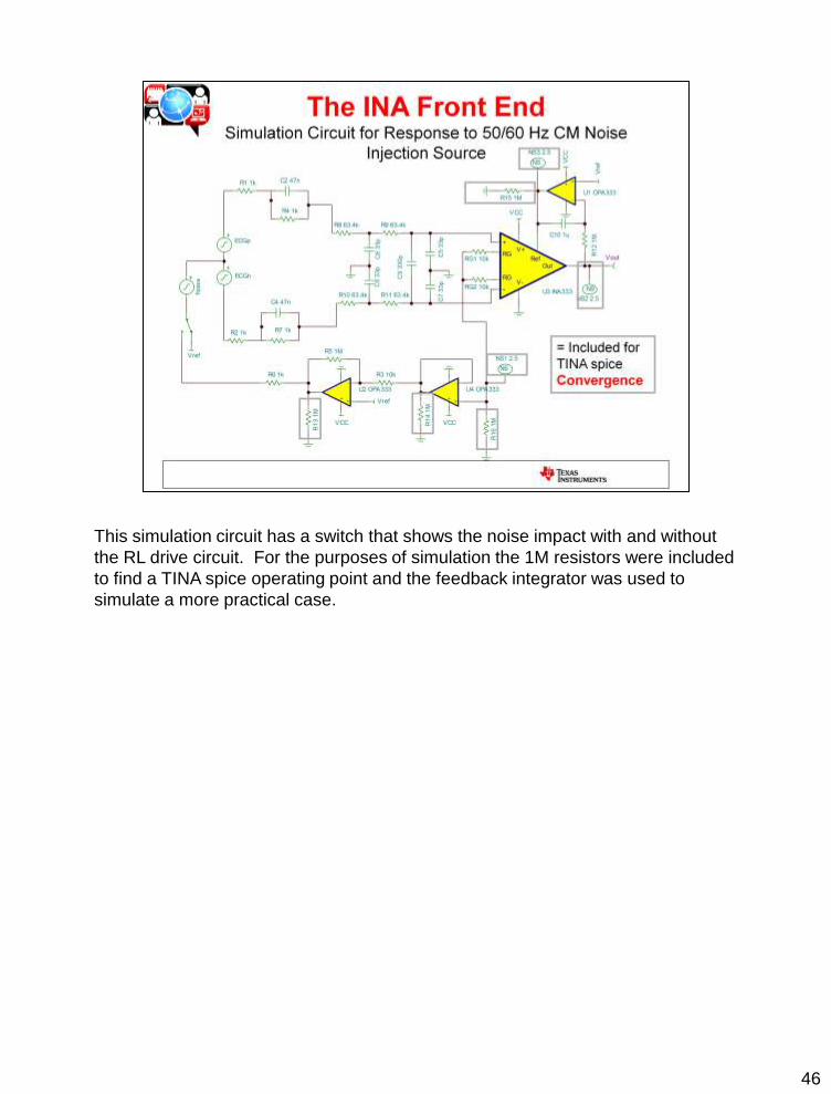
This simulation circuit has a switch that shows the noise impact with and without
the RL drive circuit. For the purposes of simulation the 1M resistors were included
to find a TINA spice operating point and the feedback integrator was used to
simulate a more practical case.

47
This plot shows the before effect with the switch connected to Vref and no RL
drive.

48
Though the noise is reduced by adding the RL drive amplifier, it is not completely
eliminated by the RL drive. This represents a very realistic case as there are often
other actions needed to reduce noise other than just a RL drive circuit.
49
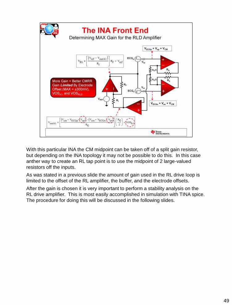
With this particular INA the CM midpoint can be taken off of a split gain resistor,
but depending on the INA topology it may not be possible to do this. In this case
anther way to create an RL tap point is to use the midpoint of 2 large-valued
resistors off the inputs.
As was stated in a previous slide the amount of gain used in the RL drive loop is
limited to the offset of the RL amplifier, the buffer, and the electrode offsets.
After the gain is chosen it is very important to perform a stability analysis on the
RL drive amplifier. This is most easily accomplished in simulation with TINA spice.
The procedure for doing this will be discussed in the following slides.
50
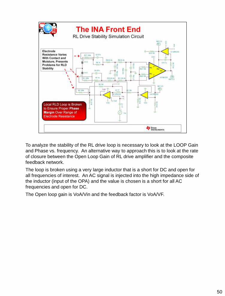
To analyze the stability of the RL drive loop is necessary to look at the LOOP Gain
and Phase vs. frequency. An alternative way to approach this is to look at the rate
of closure between the Open Loop Gain of RL drive amplifier and the composite
feedback network.
The loop is broken using a very large inductor that is a short for DC and open for
all frequencies of interest. An AC signal is injected into the high impedance side of
the inductor (input of the OPA) and the value is chosen is a short for all AC
frequencies and open for DC.
The Open loop gain is VoA/Vin and the feedback factor is VoA/VF.

51
The contact resistance of the RL drive can vary between 1k to 100k ohms so it is
necessary to analyze the feedback network for both cases. Notice that in either
case the feedback factor is increasing at 20dB/dec and AOL is decreasing at
20dB/dec. Recall that for stability it is necessary to have a rate of closure (ROC)
of <=20dB/dec; therefore, this circuit is inherently unstable and the feedback
network needs to be fixed.
In order to do this it will be necessary to look at the different pieces of the
feedback network to determine which is causing the overall feedback factor to
increase. Once this happens compensation can be added to flatten out the
feedback factor so that it intersects the AOL curve at 0dB/dec and thereby give an
ROC of 20dB/dec.
52
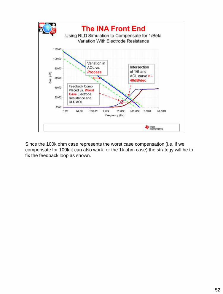
Since the 100k ohm case represents the worst case compensation (i.e. if we
compensate for 100k it can also work for the 1k ohm case) the strategy will be to
fix the feedback loop as shown.
53
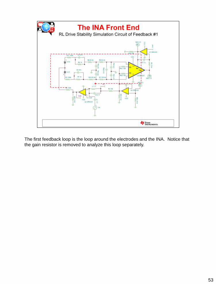
The first feedback loop is the loop around the electrodes and the INA. Notice that
the gain resistor is removed to analyze this loop separately.

54
In this case feedback #1 (i.e. that through the INA) is broken by removing the
buffer amplifier and leaving the gain resistor around the RL drive amplifier in place.
The following slide will show the impact of each feedback on the overall stability of
the oop.

55
The lowest magnitude feedback always dominates; therefore, feedback #2 has no
impact on the overall 1/beta (feedback factor) and we can concentrate our efforts
on feedback path #1.
56
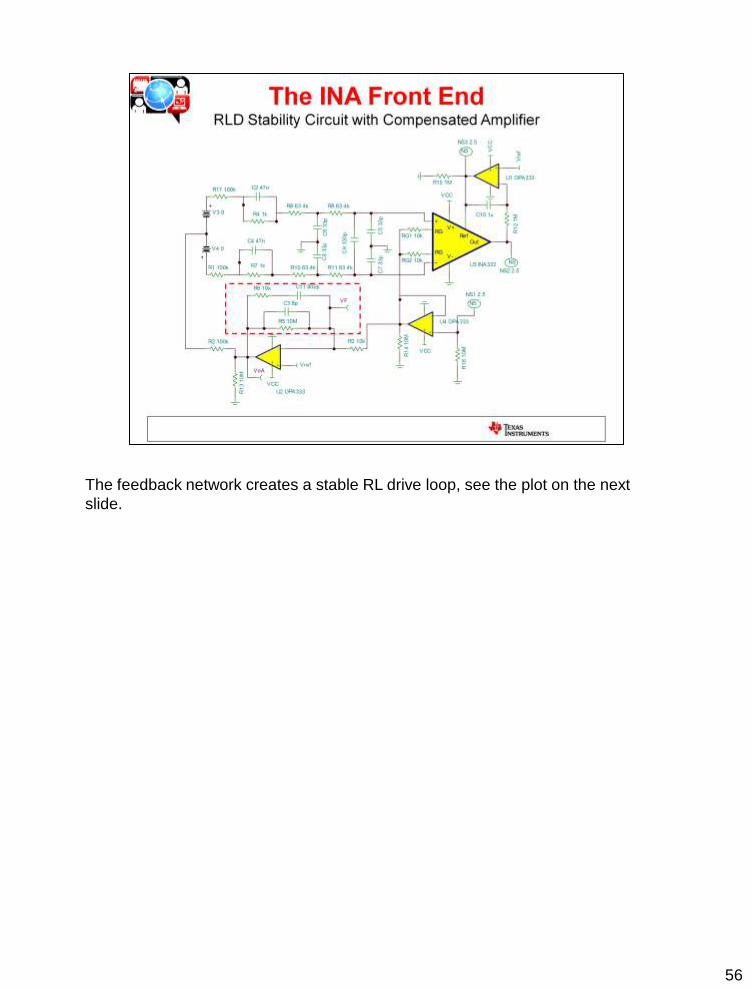
The feedback network creates a stable RL drive loop, see the plot on the next
slide.

57
This plot shows that the intersection between 1/Beta and AOL is < 20dB/dec;
therefore, we should expect to see a good time domain response in the following
slide.

58
The Loop Gain Phase confirms what the 1/Beta and AOL plots told us and shows
about 70 degrees of phase margin. This is good place to be considering the
steep roll off in phase margin with frequency. Which means that any process
variations that could make the phase margin worse will still have > 45 degrees of
margin.

59
Sometimes the frequency domain and time domain do not necessarily correlate to
a stable, well-behaved circuit due to the fact that there are some complex poles
and zeros that cause ringing in the time domain. This is the reason why it is
necessary to check a circuit both in the time domain and the frequency domain.
In this case a good clean step response is achieved with minimal settling time
which is what we need out of the RL drive amplifier.

60

61
The purpose of a shield on cables is to protect the inputs from noise pickup. In
fact, just having a shield usually comes with a significant improvement in noise
rejection; however, parasitic capacitances can cause parasitic leakage paths from
the shield to the inputs of the amplifier. Of course if these are coupled in
asymmetrically this noise will become differential and amplify to the output of the
INA.
Leakage current through these parasitic paths is dependent on a voltage
difference between the shield and the input paths; therefore, if the shield is driven
to the same common potential as the inputs, this will virtually eliminate the leakage
current induced by these parasitic capacitances.
One way to do this is to use the buffer that derives the common drive for the RL to
perform dual duty and also drive the shield.
Caution must be taken in doing this because the capacitance of the cable can
exceed 1nF, which means that most low power buffer amplifiers chosen as the
shield drive will not be inherently stable driving the cable directly. Oftentimes it is
necessary to isolate and compensate the buffer amplifier to ensure stability for this
capacitive load.
Also, an RC at the output of the shield drive amplifier can be used for low pass
filtering to reduce noise pickup.

62
This TINA circuit is used to analyze the stability of the shield drive loop with an
OPA333 assuming a 1nF load capacitance. Again, the loop is broken with a large
inductor and the intersection between AOL and 1/Beta is analyzed.

63
In this case the AOL curve breaks at -40dB/decade and intersects the 1/Beta
curve at 0dB/dec which means this buffer configuration will be inherently
unstable. The unity gain feedback of the buffer will have to be altered to
ensure that this amplifier will remain stable.
There are 2 ways to go about this:
(1) Throw away bandwidth and step the 1/Beta curve up to 40dB, flatten it out and
intersect the AOL curve at 10kHz where the AOL curve is -20dB/dec
(2) Add a pole to the 1/Beta curve around 100kHz such that it intersects the AOL
curve at -20dB/decade. This would mean that the ROC would be -40dB/dec –
(-20dB/decade) = 20dB/dec

64
T
Frequency (Hz)
1.00 10.00 100.00 1.00k 10.00k 100.00k 1.00M
Gain
(dB
)
-20.00
0.00
20.00
40.00
60.00
80.00
100.00
120.00
In this case we chose
option #2, i.e. roll off the
1/Beta curve at -20dB/dec

65
With this method of compensation not only is the phase margin > 45 degrees, but
it is relatively flat which means that with process variation we should not expect a
severe degradation in phase margin.
66

67
68

69

70

71

72

73
74

75
Now we return to the original question about which approach might be better for
ECG measurement: Gain + Filtering + SAR or 24 bit Delta Sigma?
It is clear that the SAR approach requires a good # of components and filtering
which can incur a large BOM cost, but what about the Delta-Sigma?

76
This Simulation Circuit injects differential noise into the ECG circuit to demonstrate
how couples to the output of the gain stage.
77
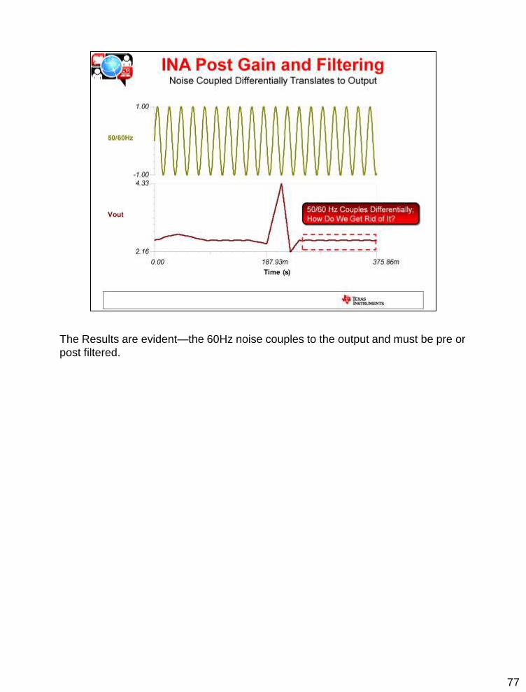
The Results are evident—the 60Hz noise couples to the output and must be pre or
post filtered.

78
Filter Pro is a free program that can be downloaded from ti.com. This program
allows you to build a custom filter based on # poles, zeros, attenuation, and filter
type. You can also maximize based on Bessel, Butterworth, and Chebyzchev
Response and also has the option of making the filter type MFB or Sallen Key.
In this example I designed a Twin-T notch at 60Hz for the ECG circuit. This
example shows a 1 pole, 1 zero response.

79
In this case I selected an OPA378 as the post gain amplifier as this device is the
lowest noise OPA that exists on a single supply.

80
60 Hz noise does not get completely removed, but it is severely reduced by the
notch filter. It might be then necessary to remove more of the noise with additional
line cycle sampling and in the ADC conversion stage.

81
This slide highlights the concept of line cycle sampling. If the circuit is designed
for both 50/60Hz sampling the common frequency between the 2 is 27.27Hz;
therefore, if the waveform is sampled at common multiples of 27.27Hz and
averaged over that number of samples this will help dramatically reduce the effect
of power line cycle noise on the output ECG waveform.

82

83
The Delta Sigma Approach requires very little additional filtering as there is
enough resolution in the converter to digitize and acquire the signal. This means
that the cost of this system can be dramatically reduced. However, in a multiple
lead ECG system, if you need to MUX between channels, does this approach save
power? The answer: maybe compared to the SAR approach, but if the
architecture allowed for low power and simultaneous sampling this would not only
open the door for less channel skew but less MUX switching would equate to a
lower power consumption.

84