65569 ids
DESCRIPTION
MIL-STD-1553 PCI CARDTRANSCRIPT

®
Data Device Corporation 105 Wilbur Place Bohemia, New York 11716 631-567-5600 Fax: 631-567-7358 www.ddc-web.com
FOR MORE INFORMATION CONTACT:
Technical Support: 1-800-DDC-5757 ext. 7771
FEATURES
• OnetoFourDualRedundantMIL-STD-1553Channels
• EnhancedMini-ACEBC/RT/MTArchitecture
• TransformerorDirectCoupled1553Channels
• 64K-WordRAMperChannel
• HighlyAutonomousBusControllerArchitecture
• MessageScheduling
• BulkDataTransfers
• DataBlockDoubleBuffering
• AsynchronousMessages
• RetriesandBusSwitching
• RTBufferingOptions
• SingleBuffering
• DoubleBuffering
• SubaddressCircularBuffering
• GlobalCircularBuffering
• SelectiveMessageMonitor
• SupportsPCIInterrupts
• IndustrialandCommercialTemperatureRangesAvailable
DESCRIPTION
The BU-65569iX PCI card includes one to four dual redundant MIL-STD-1553 channels. The design of the BU-65569iX leverages the DDC’s Enhanced Mini-ACE®. Each channel may be independently programmed for BC/RT/Monitor, or RT/Monitor mode.
Advanced architectural features of the Enhanced Mini-ACE include a highly autonomous bus controller, an RT providing a wide variety of buffering options, and a selective message monitor. Each Enhanced Mini-ACE channel incorporates 64K words of RAM, and utilizes 3.3-volt logic to reduce power consumption.
SOFTWARE
The BU-65569iX is supported by free software, including a C library and a Windows® 9x/2000/XP, Windows NT®, and Linux driver. The library and driver comprise a suite of C function calls that serves to offload a great deal of low-level tasks from the application program-mer. This software supports all of the Enhanced Mini-ACE's advanced architectural features.
© 2002 Data Device CorporationAll trademarks are the property of their respective owners.
BU-65569i
MIL-STD-1553PCICARD
Make sure the next Card you purchase has...

2Data Device Corporation www.ddc-web.com
BU-65569iH-4/10-0
FIG
UR
E 1
. BU
-655
69iX
BL
OC
K D
IAG
RA
M
BU
-618
64
BU
-618
64
BU
-618
64
BU
-618
64
PC
IB
ridge
32-b
it,33
MH
zP
CIb
us
1 to
4M
IL-S
TD
-155
3D
ual R
edun
dant
Bus
es

3Data Device Corporation www.ddc-web.com
BU-65569iH- 4/10-0
TABLE 1. BU-65569IX SPECIFICATION TABLE
PARAMETER MIN. TYP. MAX.
ABSOLUTE MAXIMUM RATINGSSupply Voltage+5 V 7.0-0.3
UNITS
V
RECEIVERInput Impedance, Transformer Coupled (Notes 1 - 3)Threshold Voltage, Transformer CoupledCommon Mode Voltage (Note 4)
0.86010
1.0000.200
kOhmVP-P
VPEAK
TRANSMITTERDifferential Output VoltageTransformer Coupled Across 70 Ohms
Output Offset Voltage, Transformer Coupled Across 70 OhmsRise/Fall Time
20150150
27250300
18-250100
VP-PmVPEAK
ns
POWER SUPPLY REQUIREMENTSVoltages/Tolerances+3.3 V (Logic Power, Internally Generated)
+5 V (RAM and Transceiver Power)Current DrainBU-65569i1
+5 V• Idle• 25% Duty Transmitter Cycle• 50% Duty Transmitter Cycle• 100% Duty Transmitter Cycle
+3.3 V (Logic)BU-65569i2
+5 V• Idle• 25% Duty Transmitter Cycle• 50% Duty Transmitter Cycle• 100% Duty Transmitter Cycle
+3.3 V (Logic)BU-65569i3
+5 V• Idle• 25% Duty Transmitter Cycle• 50% Duty Transmitter Cycle• 100% Duty Transmitter Cycle
+3.3 V (Logic)BU-65569i4
+5 V• Idle• 25% Duty Transmitter Cycle• 50% Duty Transmitter Cycle• 100% Duty Transmitter Cycle
+3.3 V (Logic)
3.35.0
3.65.5
10021032054080
2004206401.08120
3006309601.62160
4008401.282.16200
3.04.75
VV
mAmAmAmAmA
mAmAmAA
mA
mAmAmAA
mA
mAmAAA
mA
POWER DISSIPATIONBU-65569i1
• Idle• 25% Duty Transmitter Cycle• 50% Duty Transmitter Cycle• 100% Duty Transmitter Cycle
BU-65569i2• Idle• 25% Duty Transmitter Cycle• 50% Duty Transmitter Cycle• 100% Duty Transmitter Cycle
BU-65569i3• Idle• 25% Duty Transmitter Cycle• 50% Duty Transmitter Cycle• 100% Duty Transmitter Cycle
0.841.121.411.98
1.532.102.673.81
2.233.083.935.64
WWWW
WWWW
WWWW

4Data Device Corporation www.ddc-web.com
BU-65569iH-4/10-0
TABLE 1. BU-65569IX SPECIFICATION TABLE (CONT.)
PARAMETER MIN. TYP. MAX.
POWER DISSIPATION (CONT.)BU-65569i4
• Idle• 25% Duty Transmitter Cycle• 50% Duty Transmitter Cycle• 100% Duty Transmitter Cycle
2.924.065.207.47
UNITS
WWWW
1553 MESSAGE TIMINGCompletion of CPU Write (BC Start)-to-Start ofNext Message (Non-Enhanced BC Mode)
BC Intermessage Gap - (Note 5)Non-Enhanced (Mini-ACE Compatible) BC ModeEnhanced BC Mode (Note 6)
BC/RT/MT Response Timeout (Note 7)18.5 Nominal22.5 Nominal50.5 Nominal128.0 NominalRT Response Time (Mid-Parity to Mid-Sync) (Note 8)Transmitter Watchdog Timeout
2.5
9.510.0 to 10.5
18.522.550.5
129.5
660.5
19.523.551.5131
7
17.521.549.5127
4
µs
µsµs
µsµsµsµsµsµs
THERMALAmbient Operating Temperature Range (BU-65569iX-200)Ambient Operating Temperature Range (BU-65569iX-300)Storage Temperature Range
+85+55+85
-400
-40
°C°C°C
PHYSICAL CHARACTERISTICSSize
Weight (4 channel card)
6.875(L) X 4.200(H)(172.72 X 106.68)
5.50(156)
in(mm)
oz(g)
Notes: (Notes 1 through 3 are applicable to the Input Impedance specification.)
(1) The specifications are applicable for both unpowered and powered conditions. (2) The specifications assume a 2-volt rms balanced, differential, sinusoidal input. The applicable frequency range is 75 kHz to 1 MHz. (3) Minimum impedance is guaranteed over the operating range, but is not tested. (4) Assumes a common-mode voltage within the frequency range of dc to 2 MHz, applied to pins of the isolation transformer on the stub side
(transformer coupled), and referenced to signal. (5) Typical value for minimum intermessage gap time. Under software control, this may be lengthened to 65,535 µs - message time, in incre-
ments of 1 µs. If ENHANCED CPU ACCESS, bit 14 of Configuration Register #6, is set to logic "1", then host accesses during BC Start-of-Message (SOM) and End-of-Message (EOM) transfer sequences could have the effect of lengthening the intermessage gap time. For each host access during an SOM or EOM sequence, the intermessage gap time will be lengthened by 6 clock cycles. Since there are 7 internal transfers during SOM, and 5 during EOM, this could theoretically lengthen the intermessage gap by up to 72 clock cycles; i.e., up to 7.2 µs with a 10 MHz clock, 6.0 µs with a 12 MHz clock, 4.5 µs with a 16 MHz clock, or 3.6 µs at 20 MHz clock.
(6) For enhanced BC mode, the typical value for intermessage gap time is approximately 10 clock cycles longer than for the non-enhanced BC mode. That is, an addition of 1.0 µs at 10 MHz, 833 ns at 12 MHz, 625 ns at 16 MHz, or 500 ns at 20 MHz.
(7) Software programmable (4 options). Includes RT-to-RT Timeout (measured mid parity of transmit Command Word to mid-sync of Transmitting RT Status Word).
(8) Measured from mid-parity crossing of Command Word to mid-sync crossing of RT's Status Word. (9) Power dissipation specifications assume a transformer coupled configuration with external dissipation (while transmitting) of: 0.14 watts for the active isolation transformer 0.08 watts for the active bus coupling transformer 0.45 watts for each of the two bus isolation resistors and 0.15 watts for each of the two bus termination resistors

5Data Device Corporation www.ddc-web.com
BU-65569iH- 4/10-0
INTRODUCTION
The BU-65569iX is a single-channel or multi-channel MIL-STD-1553 PCI card. The BU-65569iX is available with one to four dual redundant 1553 channels. The design of the BU-65569iX leverages the BU-61864 Enhanced Mini-ACE. Each channel may be independently programmed for BC/RT/Monitor, or RT/Monitor mode.
Advanced architectural features of the Enhanced Mini-ACE include a highly autonomous bus controller, an RT providing a wide variety of buffering options, and a selective message moni-tor. Each Enhanced Mini-ACE channel incorporates 3.3-volt logic to reduce power consumption and 64K words of RAM.
The BU-65569iX is supported by free software, including a C library and a Windows® 9x/2000/XP and Windows NT® driver. The library and driver comprise a suite of C function calls that serves to offload a great deal of low-level tasks from the applica-tion programmer. This software supports all of the Enhanced Mini-ACE's advanced architectural features. Library and driver support is also available for Linux.
ENHANCED MINI-ACE
The BU-65569iX PCI card incorporates a PCI bridge, along with between one and four of DDC's BU-61864 Enhanced Mini-ACE hybrids. Each Enhanced Mini-ACE comprises a complete, inde-pendent interface between the PCI Bridge and a MIL-STD-1553 bus. The Enhanced Mini-ACE hybrids provide software compati-bility with DDC's older generation ACE and Mini-ACE (Plus) ter-minals.
The BU-61864 Enhanced Mini-ACE provides complete multipro-tocol support of MIL-STD-1553A/B/McAir and STANAG 3838. These hybrids include dual transceivers along with protocol, host interface, memory management logic; and 64K X 16 of RAM. There is built-in parity checking for this RAM.
The Enhanced Mini-ACE’s include a 5V, voltage source trans-ceiver for improved line driving capability, with options for MIL-STD-1760 compliance (20 VP-P minimum transmitter voltage) or McAir compatibility (consult factory). As a means of reducing power consumption, the Mini-ACE’s logic is powered by 3.3V.
One of the new salient features of the Enhanced Mini-ACE is its new bus controller architecture. The Enhanced BC's highly autonomous message sequence control engine provides a means for offloading the host processor for implementing multi-frame message scheduling, message retry and bus switching schemes, data double buffering, and asynchronous message insertion. In addition, the Enhanced BC mode includes 8 general purpose flag bits, a general purpose queue, and user-defined
interrupts, for the purpose of performing messaging to the host processor.
Another important feature for the Enhanced Mini-ACE is the incorporation of a fully autonomous built-in self-test. This test provides comprehensive testing of the internal protocol logic. A separate test verifies the operation of the Enhanced Mini-ACE's internal RAM. Since the self-tests are fully autonomous, they eliminate the need for the host to write and read stimulus and response vectors.
The Enhanced Mini-ACE RT offers the choice of single, double, and circular buffering for individual subaddresses or a global circular buffering option for multiple (or all) receive subaddress-es, a 50% rollover interrupt for circular buffers, an interrupt status queue for logging up to 32 interrupt events, and an option to automatically initialize to RT mode with the Busy bit set.
PCI INTERFACEAs a means of minimizing power consumption and dissipation, the design of the standard BU-65569iX board utilizes +3.3 volt power for the PCI interface and 1553 (Enhanced Mini-ACE) logic, and +5 volt power for the 1553 transceivers and RAM.
The BU-65569iX's PCI interface is a fully compliant target (slave) agent, as defined by the PCI Local Bus Specification Revision 2.2, using a 32-bit interface that operates at clock speeds of up to 33 MHz, in a 3.3 volt or 5 volt signaling environment. The interface supports PCI interrupts and contains a 32 X 32 FIFO to accelerate burst write transfers from the PCI host. That is, it's possible to perform a burst write of 32 16-bit words (i.e., all of the data words of a 1553 message) by means of sixteen 32-bit PCI transfers in approximately 500 ns.
The BU-65569iX contains only a single set of configuration reg-isters such that all of the Enhanced Mini-ACE(s) memory and register space may be addressed through a single PCI function.
Internal registers implement the Subsystem Vendor and Device ID. There are two Base Address Registers, utilized to implement the Enhanced Mini-ACE memory space (BAR0) and register space (BAR1). The Base Address Register mapping is contained in PCI configuration register space.
The ACE register mapping is located in PCI memory space, allowing for full PCI access to all 1553 terminals. The BU-65569iX configuration registers and the Enhanced Mini-ACE RAM (64K X 16 each) are accessed in 32-bit words, while all ACE registers are accessed as 16-bit words. If a 32-bit read is performed from the PCI bus in ACE register space only the first 16 bits of data are valid. ACE memory may also be accessed in 16-bit words, but memory is accessed sequentially, allowing for 32-bits of data to be written to or read from the PCI bus.

6Data Device Corporation www.ddc-web.com
BU-65569iH-4/10-0
That is, if a 32-bit PCI memory read is performed, the first 16 bits of data would be read from the requested address, the next 16 bits of data would be read from the initial address + 2. The BU-65569iX supports 32-bit and 16-bit read and write operations only. 8-bit accesses are illegal.
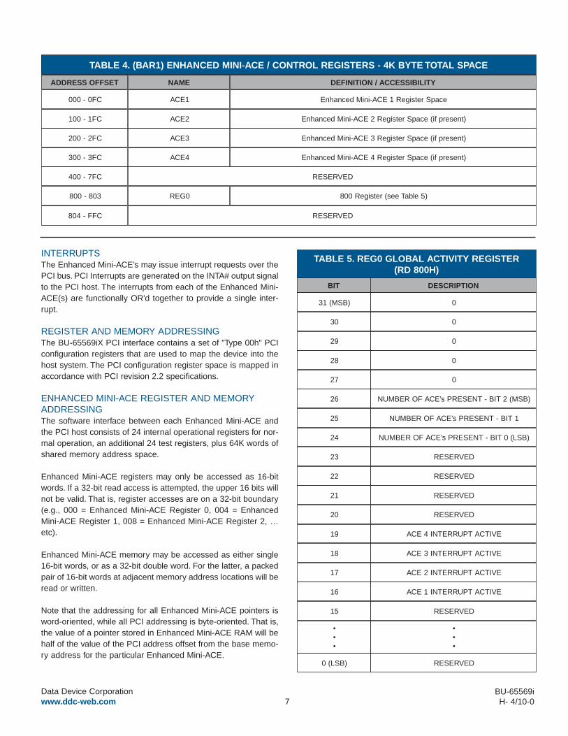
ENHANCED MINI-ACE REGISTER SPACE (ENHANCED MINI-ACE 1 - 4)
This address space (see Table 4) allows access to Enhanced Mini-ACE registers. Each 256-byte segment of allocated address space allows access to a total of 64 Enhanced Mini-ACE regis-ters per segment. Register access is on a 32-bit boundary (e.g. 000 = Enhanced Mini-ACE Register 0, 004 = Enhanced Mini-ACE Register 1, 008 = Enhanced Mini-ACE Register 2, etc).
NUMBER OF ENHANCED MINI-ACE’S PRESENTBits 26 (MSB) to 24 (LSB) provide a binary representation of the number of ACE terminals presently installed and operating (see Tables 4 and 5).
ENHANCED MINI-ACE INTERRUPT ACTIVEBits 19 through 16 represent the respective state of the Enhanced Mini-ACE4 through Enhanced Mini-ACE1 interrupt output sig-nals. All Enhanced Mini-ACE interrupts must be programmed for level operation. When an Enhanced Mini-ACE interrupt signal occurs, the corresponding ENHANCED MINI-ACE INTERRUPT ACTIVE bit gets set to a 1. Bits 19 to 16 are cleared when the respective Enhanced Mini-ACE interrupt request output is cleared (see Tables 4 and 5).
TABLE 3. (BAR0) ACE MEMORY
ADDRESS OFFSET DEFINITION
00000 - 1FFFC ACE 1 Memory Space
40000 - 5FFFC ACE 3 Memory Space (if present)
60000 - 7FFFC ACE 4 Memory Space (if present)
ACE 2 Memory Space (if present)20000 - 3FFFC
TABLE 2. PCI CONFIGURATION REGISTER SPACE
ADDRESS 31 24 23 16 15 8
00h
Vendor IDDevice ID
7 0
04h Command RegisterStatus Register
08h Class Code = 078000 h Rev ID = 01
0ChHeader Type
00hLatency Timer
BIST(Not Implemented)
Cache Line Size
0zh(z = 1 to 4 and represents
the channel count)0Bh
DDC Manufacturer Device ID value(4DDCH)
10hBase Address Register 0 (for Enhanced Mini-ACE RAM)
R/W and 0’ssee text
R/W 00h 04h
14hBase Address Register 1 (for Enhanced Mini-ACE Registers)
R/WR/WR/W and 0’s
see text04h
18h - 24hBase Address Registers 2 through 5 (not used)
00000000h
28h Card Bus CIS pointer (Not Used) 00000000h
2Ch Subsystem Device and Subsystem Vendor ID
30h Expansion ROM Base Address (Not Used, bit 0 = 0)
34h - 38h Reserved
3ChMax Lat.
00hMin Gnt
00hInterrupt Pin
01hInterrupt Line
R/W
7Data Device Corporation www.ddc-web.com
BU-65569iH- 4/10-0
INTERRUPTSThe Enhanced Mini-ACE’s may issue interrupt requests over the PCI bus. PCI Interrupts are generated on the INTA# output signal to the PCI host. The interrupts from each of the Enhanced Mini-ACE(s) are functionally OR'd together to provide a single inter-rupt.
REGISTER AND MEMORY ADDRESSINGThe BU-65569iX PCI interface contains a set of "Type 00h" PCI configuration registers that are used to map the device into the host system. The PCI configuration register space is mapped in accordance with PCI revision 2.2 specifications.
ENHANCED MINI-ACE REGISTER AND MEMORY ADDRESSINGThe software interface between each Enhanced Mini-ACE and the PCI host consists of 24 internal operational registers for nor-mal operation, an additional 24 test registers, plus 64K words of shared memory address space.
Enhanced Mini-ACE registers may only be accessed as 16-bit words. If a 32-bit read access is attempted, the upper 16 bits will not be valid. That is, register accesses are on a 32-bit boundary (e.g., 000 = Enhanced Mini-ACE Register 0, 004 = Enhanced Mini-ACE Register 1, 008 = Enhanced Mini-ACE Register 2, … etc).
Enhanced Mini-ACE memory may be accessed as either single 16-bit words, or as a 32-bit double word. For the latter, a packed pair of 16-bit words at adjacent memory address locations will be read or written.
Note that the addressing for all Enhanced Mini-ACE pointers is word-oriented, while all PCI addressing is byte-oriented. That is, the value of a pointer stored in Enhanced Mini-ACE RAM will be half of the value of the PCI address offset from the base memo-ry address for the particular Enhanced Mini-ACE.
TABLE 4. (BAR1) ENHANCED MINI-ACE / CONTROL REGISTERS - 4K BYTE TOTAL SPACE
ADDRESS OFFSET NAME DEFINITION / ACCESSIBILITY
000 - 0FC
Enhanced Mini-ACE 2 Register Space (if present)
ACE1
200 - 2FC Enhanced Mini-ACE 3 Register Space (if present)ACE3
300 - 3FC ACE4 Enhanced Mini-ACE 4 Register Space (if present)
400 - 7FC RESERVED
Enhanced Mini-ACE 1 Register Space
ACE2
800 - 803 REG0
RESERVED
100 - 1FC
800 Register (see Table 5)
804 - FFC
TABLE 5. REG0 GLOBAL ACTIVITY REGISTER (RD 800H)
BIT DESCRIPTION
31 (MSB) 0
29 0
28 0
030
27 0
25 NUMBER OF ACE’s PRESENT - BIT 1
24 NUMBER OF ACE’s PRESENT - BIT 0 (LSB)
NUMBER OF ACE’s PRESENT - BIT 2 (MSB)26
23 RESERVED
21 RESERVED
20 RESERVED
RESERVED22
19 ACE 4 INTERRUPT ACTIVE
18 ACE 3 INTERRUPT ACTIVE
16 ACE 1 INTERRUPT ACTIVE
15 RESERVED
ACE 2 INTERRUPT ACTIVE17
•••
•••
0 (LSB) RESERVED

8Data Device Corporation www.ddc-web.com
BU-65569iH-4/10-0
For normal operation, the host processor only needs to access the lower 32 register address locations (00-1F). The next 32 locations (20-3F) should be reserved, since many of these are used for factory test.
BUS CONTROLLER (BC) ARCHITECTUREThe BC functionality for the Enhanced Mini-ACE includes two separate architectures: (1) the older, non-Enhanced mode, which provides complete compatibility with the previous ACE and Mini-ACE (Plus) generation products; and (2) the newer, Enhanced BC mode. The Enhanced BC mode offers several new powerful architectural features. These include the incorporation of a highly autonomous BC message sequence control engine, which greatly serves to offload the operation of the host CPU.
The Enhanced BC's message sequence control engine provides a high degree of flexibility for implementing major and minor frame scheduling; capabilities for inserting asynchronous mes-sages in the middle of a frame; to separate 1553 message data from control/status data for the purpose of implementing double buffering and performing bulk data transfers; for implementing message retry schemes, including the capability for automatic bus channel switchover for failed messages; and for reporting various conditions to the host processor by means of 4 user-defined interrupts and a general purpose queue.
In both the non-Enhanced and Enhanced BC modes, the Enhanced Mini-ACE BC implements all MIL-STD-1553B mes-sage formats. Message format is programmable on a message-by-message basis by means of the BC Control Word and the T/R bit of the Command Word for the respective message. The BC Control Word allows 1553 message format, 1553A/B type RT, bus channel, self-test, and Status Word masking to be specified on an individual message basis. In addition, automatic retries and/or interrupt requests may be enabled or disabled for indi-vidual messages. The BC performs all error checking required by MIL-STD-1553B. This includes validation of response time, sync type and sync encoding, Manchester II encoding, parity, bit count, word count, Status Word RT Address field, and various RT-to-RT transfer errors. The Enhanced Mini-ACE BC response timeout value is programmable with choices of 18, 22, 50, and 130 µs. The longer response timeout values allow for operation over long buses and/or use of the repeaters.
In its non-Enhanced mode, the Enhanced Mini-ACE may be pro-grammed to process BC frames of up to 512 messages with no processor intervention. In the Enhanced BC mode, there is no explicit limit to the number of messages that may be processed in a frame. In both modes, it is possible to program for either single frame or frame auto-repeat operation. In the auto-repeat mode, the frame repetition rate may be controlled either internally, using a programmable BC frame timer, or from an external trigger input.
ENHANCED BC MODE: MESSAGE SEQUENCE CONTROLOne of the major new architectural features of the Enhanced Mini-ACE series is its advanced capability for BC message sequence control. The Enhanced Mini-ACE supports highly autonomous BC operation, which greatly offloads the operation of the host processor.
The operation of the Enhanced Mini-ACE's message sequence control engine is illustrated in Figure 2. The BC message sequence control involves an instruction list pointer register; an instruction list which contains multiple 2-word entries; a message control/status stack, which contains multiple 8-word or 10-word descriptors; and data blocks for individual mes-sages.
The initial value of the instruction list pointer register is initialized by the host processor (via Register 0D), and is incremented by the BC message sequence processor (host readable via Register 03). During operation, the message sequence control processor fetches the operation referenced by the instruction list pointer register from the instruction list.
Note that the pointer parameter referencing the first word of a message's control/status block (the BC Control Word) must con-tain an address value that is modulo 8. Also, note that if the mes-sage is an RT-to-RT transfer, the pointer parameter must contain an address value that is modulo 16.
OP CODESThe instruction list pointer register references a pair of words in the BC instruction list: an op code word, followed by a parameter word. The format of the op code word, which is illustrated in Figure 3, includes a 5-bit op code field and a 5-bit condition code field. The op code identifies the instruction to be executed by the BC message sequence controller.
OP CODE
DATA BLOCK
MESSAGECONTROL/STATUS
PARAMETER(POINTER)
BLOCK
BC INSTRUCTIONLIST
BC INSTRUCTIONLIST POINTER REGISTER
BC CONTROLWORD
COMMAND WORD(Rx Command forRT-to-RT transfer)
DATA BLOCK POINTER
TIME-TO-NEXT MESSAGE
TIME TAG WORD
BLOCK STATUS WORD
LOOPBACK WORD
RT STATUS WORD
2nd (Tx) COMMAND WORD(for RT-to-RT transfer)
2nd RT STATUS WORD(for RT-to-RT transfer)
INITIALIZE BY REGISTER0D (RD/WR); READ CURRENT
VALUE VIA REGISTER 03(RD ONLY)
FIGURE 2. BC MESSAGE SEQUENCE CONTROL

9Data Device Corporation www.ddc-web.com
BU-65569iH- 4/10-0
Most of the operations are conditional, with execution dependent on the contents of the condition code field. Bits 3 - 0 of the condi-tion code field identify the particular condition. Bit 4 of the condi-tion code field identifies the logic sense ("1" or "0") of the selected condition code on which the conditional execution is dependent. Table 33 lists all the op codes, along with their respective mnemonic, code value, parameter, and description. Table 34 defines all the condition codes.
Eight of the condition codes (8 through F) are set or cleared as the result of the most recent message. The other eight are defined as "General Purpose" condition codes GP0 through GP7. There are three mechanisms for programming the values of the General Purpose Condition Code bits: (1) They may be set, cleared, or toggled by the host processor, by means of the BC GENERAL PURPOSE FLAG REGISTER; (2) they may be set, cleared, or toggled by the BC message sequence control processor, by means of the GP Flag Bits (FLG) instruction; and (3) GP0 and GP1 only (but none of the others) may be set or cleared by means of the BC message sequence control proces-sor's Compare Frame Timer (CFT) or Compare Message Timer (CMT) instructions.
The host processor also has read-only access to the BC condi-tion codes by means of the BC CONDITION CODE REGISTER.
Note that four (4) instructions are unconditional. These are Compare to Frame Timer (CFT), Compare to Message Timer (CMT), GP Flag Bits (FLG), and Execute and Flip (XQF). For these instructions, the Condition Code Field is "don't care". That is, these instructions are always executed, regardless of the result of the condition code test.
All other instructions are conditional. That is, they will only be executed if the condition code specified by the condition code field in the op code word tests true. If the condition code field tests false, the instruction list pointer will skip down to the next instruc-tion.
As shown in Table 33, many of the operations include a single-word parameter. For an XEQ (execute message) operation, the parameter is a pointer to the start of the message's control/status block. For other operations, the parameter may be an address, a time value, an interrupt pattern, a mechanism to set or clear general purpose flag bits, or an immediate value. For several op codes, the parameter is "don't care" (not used).
As described above, some of the op codes will cause the mes-sage sequence control processor to execute messages. In this case, the parameter references the first word of a message con-trol/status block. With the exception of RT-to-RT transfer mes-sages, all message status/control blocks are eight words long: a block control word, time-to-next-message parameter, data block pointer, command word, status word, loopback word, block sta-tus word, and time tag word.
In the case of an RT-to-RT transfer message, the size of the mes-sage control/status block increases to 16 words. However, in this case, the last six words are not used; the ninth and tenth words are for the second command word and second status word.
The third word in the message control/status block is a pointer that references the first word of the message's data word block. Note that the data word block stores only data words, which are to be either transmitted or received by the BC. By segregating data words from command words, status words, and other con-trol and "housekeeping" functions, this architecture enables the use of convenient, usable data structures, such as circular buf-fers and double buffers.
Other operations support program flow control; i.e., jump and call capability. The call capability includes maintenance of a call stack, which supports a maximum of four (4) entries; there is also a return instruction. In the case of a call stack overrun or under-run, the BC will issue a CALL STACK POINTER REGISTER ERROR interrupt, if enabled.
Other op codes may be used to delay for a specified time; start a new BC frame; wait for an external trigger to start a new frame; do comparisons based on frame time and time-to-next message; load the time tag or frame time registers; halt; and issue host interrupts. In the case of host interrupts, the message control processor passes a 4-bit user-defined interrupt vector to the host, by means of the Enhanced Mini-ACE's Interrupt Status Register.
The purpose of the FLG instruction is to enable the message sequence controller to set, clear, or toggle the value(s) of any or all of the eight general purpose condition flags.
The op code parity bit encompasses all sixteen bits of the op code word. This bit must be programmed for odd parity. If the message sequence control processor fetches an undefined op code word, an op code word with even parity, or bits 9-5 of an op code word do not have a binary pattern of 01010, the message sequence control processor will immediately halt the BC's opera-tion. In addition, if enabled, a BC TRAP OP CODE interrupt will
15 14 13 12 11 10 9 8 7 6 5 4 3 2 1 0
Odd Parity
OpCode Field 0 1 0 1 0 Condition Code Field
FIGURE 3. BC OP CODE FORMAT

10Data Device Corporation www.ddc-web.com
BU-65569iH-4/10-0
be issued. Also, if enabled, a parity error will result in an OP CODE PARITY ERROR interrupt.
The Enhanced Mini-ACE BC message sequence control capabil-ity enables a high degree of offloading of the host processor. This includes using the various timing functions to enable autono-mous structuring of major and minor frames. In addition, by implementing conditional jumps and subroutine calls, the mes-sage sequence control processor greatly simplifies the insertion of asynchronous, or "out-of-band" messages.
EXECUTE AND FLIP OPERATIONThe Enhanced Mini-ACE BC's XQF, or "Execute and Flip" opera-tion, provides some unique capabilities. Following execution of this unconditional instruction, if the condition code tests TRUE, the BC will modify the value of the current XQF instruction's pointer parameter by toggling bit 4 in the pointer. That is, if the selected condition flag tests true, the value of the parameter will be updated to the value = old address XOR 0010h. As a result, the next time that this line in the instruction list is executed, the Message Control/Status Block at the updated address (old address XOR 0010h), rather than the one at the old address, will be processed. The operation of the XQF instruction is illustrated in Figure 4.
There are multiple ways of utilizing the "execute and flip" func-tionality. One is to facilitate the implementation of a double buffer-ing data scheme for individual messages. This allows the mes-sage sequence control processor to "ping-pong" between a pair of data buffers for a particular message. By so doing, the host
processor can access one of the two Data Word blocks, while the BC reads or writes the alternate Data Word block.
A second application of the "execute and flip" capability is in asso-ciation with message retries. This allows the BC to not only switch buses when retrying a failed message, but to automatically switch buses permanently for all future times that the same message is to be processed. This not only provides a high degree of autonomy from the host CPU, but also saves BC bandwidth, by eliminating future attempts to process messages on an RT's failed channel.
GENERAL PURPOSE QUEUEThe Enhanced Mini-ACE BC allows for the creation of a general purpose queue. This data structure provides a means for the message sequence processor to convey information to the BC host. The BC op code repertoire provides mechanisms to push various items on this queue. These include the contents of the Time Tag Register, the Block Status Word for the most recent message, an immediate data value, or the contents of a specified memory address.
Figure 5 illustrates the operation of the BC General Purpose Queue. Note that the BC General Purpose Queue Pointer Register will always point to the next address location (modulo 64); that is, the location following the last location written by the BC message sequence control engine.
If enabled, a BC GENERAL PURPOSE QUEUE ROLLOVER interrupt will be issued when the value of the queue pointer address rolls over at a 64-word boundary.
XQF
POINTER XX00h
BC INSTRUCTION LIST MESSAGECONTROL/STATUS
BLOCK 0
DATA BLOCK 0
XX10h
MESSAGECONTROL/STATUS
BLOCK 1
DATA BLOCK 1
POINTER
POINTER
FIGURE 4. EXECUTE AND FLIP (XQP) OPERATION
LAST LOCATION
BC GENERALPURPOSE QUEUE
(64 Locations)
BC GENERALPURPOSE QUEUEPOINTERREGISTER
NEXT LOCATION
FIGURE 5. BC GENERAL PURPOSE QUEUE

11Data Device Corporation www.ddc-web.com
BU-65569iH- 4/10-0
REGISTER
A6 DESCRIPTION / ACCESSIBILITY
0 Interrupt Mask Register #1 (RD/WR)
0 Configuration Register #1 (RD/WR)
0 Configuration Register #2 (RD/WR)
0 Start/Reset Register (W/R)
0 Non-Enhanced BC or RT Command Stack Pointer/Enhanced BC Instruction List Pointer Register (RD)
0 BC Control Word/RT Subaddress Control Word Register (RD/WR)
0 Time Tag Register (RD/WR)
0 Interrupt Status Register #1 (RD)
0 Configuration Register #3 (RD/WR)
0 Configuration Register #4 (RD/WR)
0 Configuration Register #5 (RD/WR)
0 RT/Monitor Data Stack Address Register (RD/WR)
0 BC Frame Time Remaining Register (RD)
0 BC Time Remaining to Next Message Register (RD)
0 BC Frame Time/Enhanced BC Initial Instruction Pointer/RT Last Command/MT Trigger Word Register (RD/WR)
0 RT Status Word Register (RD)
0 RT BIT Word Register (RD)
1 Test Mode Register 0
1 Test Mode Register 1
1 Test Mode Register 2
1 Test Mode Register 3
1 Test Mode Register 4
1 Test Mode Register 5
1 Test Mode Register 6
1 Test Mode Register 7
1 Configuration Register #6 (RD/WR)
1 Configuration Register #7 (RD/WR)
1 Reserved
1 BC Condition Code Register (RD)
1 BC General Purpose Flag Register (WR)
1 BIT Test Status Register (RD)
TABLE 6. ENHANCED MINI-ACE REGISTERS
ADDRESS
A5
0
0
0
0
0
0
0
0
0
1
1
1
1
1
1
1
1
0
0
0
0
0
0
0
0
1
1
1
1
1
1
A4
0
0
0
0
0
1
1
1
1
0
0
0
0
1
1
1
1
0
0
0
0
1
1
1
1
0
0
0
0
0
1
A3
0
0
1
1
1
0
0
1
1
0
0
1
1
0
0
1
1
0
0
1
1
0
0
1
1
0
0
1
1
1
0
A2
0
1
0
1
1
0
1
0
1
0
1
0
1
0
1
0
1
0
1
0
1
0
1
0
1
0
1
0
1
1
0
A1
0
0
0
0
0
0
0
0
0
0
0
0
0
0
0
0
0
0
0
0
0
0
0
0
0
0
0
0
0
0
0
A0
0/1
0/1
0/1
0/1
0/1
0/1
0/1
0/1
0/1
0/1
0/1
0/1
0/1
0/1
0/1
0/1
0/1
0/1
0/1
0/1
0/1
0/1
0/1
0/1
0/1
0/1
0/1
0/1
0/1
0/1
0/1
1 Interrupt Mask Register #2 (RD/WR)
1 Interrupt Status Register #2 (RD)
1
A7
0
0
0
0
0
0
0
0
0
0
0
0
0
0
0
0
0
0
0
0
0
0
0
0
0
0
0
0
0
0
0
0
0
0 BC General Purpose Queue Pointer/RT-MT Interrupt Status Queue Pointer Register (RD/WR)
1
1
1
1
1
1
0
1
1
1
0
1
0
0
0
0/1
0/1
0/1
01 Additional Test Mode Registers0 0 0 0 0 0/1
•••
•••
11 Additional Test Mode Registers1 1 1 1 0 0/1
ENHANCED MINI-ACE REGISTERS
The address mapping for the Enhanced Mini-ACE registers is illustrated in TABLE 6:

12Data Device Corporation www.ddc-web.com
BU-65569iH-4/10-0
TABLE 7. INTERRUPT MASK REGISTER (READ/WRITE 00H)
BIT DESCRIPTION
15(MSB) RESERVED
14 RAM PARITY ERROR
13 BC/RT TRANSMITTER TIMEOUT
12 BC/RT COMMAND STACK ROLLOVER
11 MT COMMAND STACK ROLLOVER
10 MT DATA STACK ROLLOVER
9 HANDSHAKE FAILURE
8 BC RETRY
7 RT ADDRESS PARITY ERROR
6 TIME TAG ROLLOVER
5 RT CIRCULAR BUFFER ROLLOVER
4 BC MSG/RT SUBADDRESS CONTROL WORD EOM
3 BC END OF FRAME
2 FORMAT ERROR
1 BC STATUS SET/RT MODE CODE/MT PATTERN TRIGGER
0(LSB) END OF MESSAGE
TABLE 8. CONFIGURATION REGISTER #1 (READ/WRITE 04H)
BITBC FUNCTION (Bits
11-0 Enhanced Mode Only)RT WITHOUT ALTERNATE
STATUS
RT WITH ALTERNATE STATUS (Enhanced
Mode Only)
MONITOR FUNCTION(Enhanced Mode Only, bits 12-0)
15 (MSB) RT/BC-MT (logic 0) (logic 1) (logic 1) (logic 0)
14 MT/BC-RT (logic 0) (logic 0) (logic 0) (logic 1)
13 CURRENT AREA B/A CURRENT AREA B/A CURRENT AREA B/A CURRENT AREA B/A
12 MESSAGE STOP-ON-ERROR MESSAGE MONITOR ENABLED (MMT)
MESSAGE MONITOR ENABLED (MMT)
MESSAGE MONITOR ENABLED (MMT)
11 FRAME STOP-ON-ERROR S10 TRIGGER WORD ENABLED
10 STATUS SET STOP-ON-MESSAGE
BUSY S09 START-ON-TRIGGER
9 STATUS SET STOP-ON-FRAME
SERVICE REQUEST S08 STOP-ON-TRIGGER
8 FRAME AUTO-REPEAT SSFLAG S07 NOT USED
7 EXTERNAL TRIGGER ENABLED RTFLAG (Enhanced Mode Only) S06 EXTERNAL TRIGGER ENABLED
6 INTERNAL TRIGGER ENABLED NOT USED S05 NOT USED
5 INTERMESSAGE GAP TIMER ENABLED
NOT USED S04 NOT USED
4 RETRY ENABLED NOT USED S03 NOT USED
3 DOUBLED/SINGLE RETRY NOT USED S02 NOT USED
2 BC ENABLED (Read Only) NOT USED S01 MONITOR ENABLED(Read Only)
1 BC FRAME IN PROGRESS (Read Only)
NOT USED S00 MONITOR TRIGGERED (Read Only)
0 (LSB) BC MESSAGE IN PROGRESS (Read Only)
RT MESSAGE IN PROGRESS (Enhanced mode only,Read Only)
RT MESSAGE IN PROGRESS (Read Only)
MONITOR ACTIVE (Read Only)
DYNAMIC BUS CONTROL ACCEPTANCE

13Data Device Corporation www.ddc-web.com
BU-65569iH- 4/10-0
END OF MESSAGE0(LSB)
BC STATUS SET / RT MODE CODE / MT PATTERN TRIGGER
1
FORMAT ERROR2
MT COMMAND STACK ROLLOVER
BC END OF FRAME3
RT SUBADDRESS CONTROL WORD EOM4
RT CIRCULAR BUFFER ROLLOVER5
TIME TAG ROLLOVER6
RT ADDRESS PARITY ERROR7
BC RETRY8
HANDSHAKE FAIL9
MT DATA STACK ROLLOVER10
BC/RT COMMAND STACK ROLLOVER12
TRANSMITTER TIMEOUT13
RAM PARITY ERROR14
MASTER INTERRUPT15(MSB)
DESCRIPTIONBIT
11
TABLE 9. INTERRUPT STATUS REGISTER (READ/WRITE 18H)
ENHANCED MODE CODE HANDLING0(LSB)
1553A MODE CODES ENABLE1
RTFAIL / RTFLAG WRAP ENABLE2
MT COMMAND STACK SIZE 0
BUSY RX TRANSFER DISABLE3
ILLEGAL RX TRANSFER DISABLE4
ALTERNATE STATUS WORD ENABLE5
OVERRIDE MODE T/R ERROR6
ILLEGALIZATION DISABLED7
MT DATA STACK SIZE 08
MT DATA STACK SIZE 19
MT DATA STACK SIZE 210
MT COMMAND STACK SIZE 112
BC/RT COMMAND STACK SIZE 013
BC/RT COMMAND STACK SIZE 114
ENHANCED MODE ENABLE15(MSB)
DESCRIPTIONBIT
11
TABLE 10. CONFIGURATION REGISTER #3 (READ/WRITE 1CH)
TEST MODE 00(LSB)
TEST MODE 11
TEST MODE 22
BROADCAST MASK ENA/XOR
LATCH RT ADDRESS WITH CONFIG REGISTER #53
MT TAG GAP OPTION4
VALID BUSY/NO DATA5
VALID M.E./NO DATA6
2ND RETRY ALT/SAME BUS7
1ST RETRY ALT/SAME BUS8
RETRY IF STATUS SET9
RETRY IF -A AND M.E.10
EXPANDED BC CONTROL WORD ENABLE12
MODE COMMAND OVERRIDE BUSY13
INHIBIT BIT WORD IF BUSY14
EXTERNAL BIT WORD ENABLE15(MSB)
DESCRIPTIONBIT
11
TABLE 11. CONFIGURATION REGISTER #4 (READ/WRITE 20H)
RT ADDRESS PARITY0(LSB)
RT ADDRESS 01
RT ADDRESS 12
EXPANDED CROSSING ENABLED
RT ADDRESS 23
RT ADDRESS 34
RT ADDRESS 45
RT ADDRESS LATCH/TRANSPARENT 6
BROADCAST DISABLED7
GAP CHECK ENABLED8
RESPONSE TIMEOUT SELECT 09
RESPONSE TIMEOUT SELECT 110
EXTERNAL TX INHIBIT B12
EXTERNAL TX INHIBIT A13
SINGLE-ENDED SELECT14
12 MHZ CLOCK SELECT (10 MHZ CLOCK SELECT for BU-61689)
15(MSB)
DESCRIPTIONBIT
11
TABLE 12. CONFIGURATION REGISTER #5 (READ/WRITE 24H)

14Data Device Corporation www.ddc-web.com
BU-65569iH-4/10-0
RT / MONITOR DATA STACK ADDRESS 00(LSB)
••
••
••
RT / MONITOR DATA STACK ADDRESS 1515(MSB)
DESCRIPTIONBIT
TABLE 13. RT / MONITOR DATA STACK ADDRESS REGISTER
(READ/WRITE 28H)
BC FRAME TIME REMAINING 00(LSB)
••
••
••
BC FRAME TIME REMAINING 1515(MSB)
DESCRIPTIONBIT
TABLE 14. BC FRAME TIME REMAINING REGISTER (READ/WRITE 2CH)
BC MESSAGE TIME REMAINING 00(LSB)
••
••
••
BC MESSAGE TIME REMAINING 1515(MSB)
DESCRIPTIONBIT
TABLE 15. BC MESSAGE TIME REMAINING REGISTER
(READ 30H)
Note: resolution = 1 µs per LSB
BIT 00(LSB)
••
••
••
BIT 1515(MSB)
DESCRIPTIONBIT
TABLE 16. BC FRAME TIME / RT LAST COMMAND / MT / TRIGGER REGISTER (READ 34H)
TABLE 17. RT STATUS WORD REGISTER (READ 36H)
11
BIT DESCRIPTION
15(MSB) LOGIC “0”
12 LOGIC “0”
14 LOGIC “0”
13 LOGIC “0”
10 MESSAGE ERROR
9 INSTRUMENTATION
8 SERVICE REQUEST
7 RESERVED
6 RESERVED
5 RESERVED
4 BROADCAST COMMAND RECEIVED
3 BUSY
LOGIC “0”
2 SUBSYSTEM FLAG
1 DYNAMIC BUS CONTROL ACCEPT
0(LSB) TERMINAL FLAG
COMMAND WORD CONTENTS ERROR0(LSB)
RT-to-RT 2ND COMMAND WORD ERROR1
RT-to-RT NO RESPONSE ERROR2
TRANSMITTER SHUTDOWN B
RT-to-RT GAP / SYNC / ADDRESS ERROR3
PARITY / MANCHESTER ERROR RECEIVED4
INCORRECT SYNC RECEIVED5
LOW WORD COUNT6
HIGH WORD COUNT7
BIT TEST FAIL8
TERMINAL FLAG INHIBITED9
TRANSMITTER SHUTDOWN A10
HANDSHAKE FAILURE12
LOOP TEST FAILURE A13
LOOP TEST FAILURE B14
TRANSMITTER TIMEOUT15(MSB)
DESCRIPTIONBIT
11
TABLE 18. RT BIT WORD REGISTER (READ 3CH)
Note: resolution = 100 µs per LSB

15Data Device Corporation www.ddc-web.com
BU-65569iH- 4/10-0
CLOCK SELECT 00(LSB)
CLOCK SELECT 11
64-WORD REGISTER SPACE2
GLOBAL CIRCULAR BUFFER SIZE 2
RESERVED3
ENHANCED MESSAGE MONITOR4
RT ADDRESS SOURCE5
INTERRUPT STATUS QUEUE ENABLE6
DISABLE VALID MESSAGES TO INTERRUPT STATUS QUEUE
7
DISABLE INVALID MESSAGES TO INTERRUPT STATUS QUEUE
8
GLOBAL CIRCULAR BUFFER SIZE 09
GLOBAL CIRCULAR BUFFER SIZE 110
GLOBAL CIRCULAR BUFFER ENABLE12
COMMAND STACK POINTER INCREMENT ON EOM (RT, MT)
13
ENHANCED CPU ACCESS14
ENHANCED BUS CONTROLLER15(MSB)
DESCRIPTIONBIT
11
TABLE 19. CONFIGURATION REGISTER #6 (READ/WRITE 60H)
MODE CODE RESET / INCMD SELECT0(LSB)
ENHANCED BC WATCHDOG TIMER ENABLED1
ENHANCED TIMETAG SYNCHRONIZE2
MEMORY MANAGEMENT BASE ADDRESS 11
1553B RESPONSE TIME3
RT HALT ENABLE4
RESERVED5
RESERVED6
RESERVED7
RESERVED8
RESERVED9
MEMORY MANAGEMENT BASE ADDRESS 1010
MEMORY MANAGEMENT BASE ADDRESS 1212
MEMORY MANAGEMENT BASE ADDRESS 1313
MEMORY MANAGEMENT BASE ADDRESS 1414
MEMORY MANAGEMENT BASE ADDRESS 1515(MSB)
DESCRIPTIONBIT
11
TABLE 20. CONFIGURATION REGISTER #7 (READ/WRITE 64H)
EQUAL FLAG / GENERAL PURPOSE FLAG 00(LSB)
LESS THAN FLAG / GENERAL PURPOSE FLAG 11
GENERAL PURPOSE FLAG 22
MASKED STATUS SET
GENERAL PURPOSE FLAG 33
GENERAL PURPOSE FLAG 44
GENERAL PURPOSE FLAG 55
GENERAL PURPOSE FLAG 66
GENERAL PURPOSE FLAG 77
NO RESPONSE8
FORMAT ERROR9
GOOD BLOCK TRANSFER10
BAD MESSAGE12
RETRY 013
RETRY 114
ALWAYS15(MSB)
DESCRIPTIONBIT
11
TABLE 21. BC CONDITION CODE REGISTER (READ 6CH)
SET GENERAL PURPOSE FLAG 00(LSB)
SET GENERAL PURPOSE FLAG 11
SET GENERAL PURPOSE FLAG 22
CLEAR GENERAL PURPOSE FLAG 3
SET GENERAL PURPOSE FLAG 33
SET GENERAL PURPOSE FLAG 44
SET GENERAL PURPOSE FLAG 55
SET GENERAL PURPOSE FLAG 66
SET GENERAL PURPOSE FLAG 77
CLEAR GENERAL PURPOSE FLAG 08
CLEAR GENERAL PURPOSE FLAG 19
CLEAR GENERAL PURPOSE FLAG 210
CLEAR GENERAL PURPOSE FLAG 412
CLEAR GENERAL PURPOSE FLAG 513
CLEAR GENERAL PURPOSE FLAG 614
CLEAR GENERAL PURPOSE FLAG 715(MSB)
DESCRIPTIONBIT
11
TABLE 22. BC GENERAL PURPOSE FLAG REGISTER(WRITE 6CH)

16Data Device Corporation www.ddc-web.com
BU-65569iH-4/10-0
NOT USED0(LSB)
BIT TEST COMPLETE1
ENHANCED BC IRQ02
CALL STACK POINTER REGISTER ERROR
ENHANCED BC IRQ13
ENHANCED BC IRQ24
ENHANCED BC IRQ35
MONITOR DATA STACK 50% ROLLOVER6
MONITOR COMMAND STACK 50% ROLLOVER7
RT CIRCULAR BUFFER 50% ROLLOVER8
RT COMMAND STACK 50% ROLLOVER9
BC TRAP OP CODE10
GENERAL PURPOSE QUEUE / INTERRUPT STATUS QUEUE ROLLOVER
12
RT ILLEGAL COMMAND13
BC OP CODE PARITY ERROR14
NOT USED15(MSB)
DESCRIPTIONBIT
11
TABLE 24. INTERRUPT MASK REGISTER #2 (READ/WRITE 74H)
INTERRUPT CHAIN BIT0(LSB)
BIT TEST COMPLETE1
ENHANCED BC IRQ02
CALL STACK POINTER REGISTER ERROR
ENHANCED BC IRQ13
ENHANCED BC IRQ24
ENHANCED BC IRQ35
MONITOR DATA STACK 50% ROLLOVER6
MONITOR COMMAND STACK 50% ROLLOVER7
RT CIRCULAR BUFFER 50% ROLLOVER8
RT COMMAND STACK 50% ROLLOVER9
BC TRAP OP CODE10
GENERAL PURPOSE QUEUE / INTERRUPT STATUS QUEUE ROLLOVER
12
ILLEGAL COMMAND13
BC OP CODE PARITY ERROR14
MASTER INTERRUPT15(MSB)
DESCRIPTIONBIT
11
TABLE 25. INTERRUPT STATUS REGISTER #2(READ 78H)
QUEUE POINTER ADDRESS 00(LSB)
QUEUE POINTER ADDRESS 11
QUEUE POINTER ADDRESS 22
QUEUE POINTER BASE ADDRESS 11
QUEUE POINTER ADDRESS 33
QUEUE POINTER ADDRESS 44
QUEUE POINTER ADDRESS 55
QUEUE POINTER BASE ADDRESS 66
QUEUE POINTER BASE ADDRESS 77
QUEUE POINTER BASE ADDRESS 88
QUEUE POINTER BASE ADDRESS 99
QUEUE POINTER BASE ADDRESS 1010
QUEUE POINTER BASE ADDRESS 1212
QUEUE POINTER BASE ADDRESS 1313
QUEUE POINTER BASE ADDRESS 1414
QUEUE POINTER BASE ADDRESS 1515(MSB)
DESCRIPTIONBIT
11
TABLE 26. BC GENERAL PURPOSE QUEUE POINTER REGISTER /
RT, MT INTERRUPT STATUS QUEUE POINTER REGISTER
(READ/WRITE 7CH)
LOGIC “0”0(LSB)
LOGIC “0”1
LOGIC “0”2
LOGIC “1”
LOGIC “0”3
LOGIC “0”4
RAM BUILT-IN TEST PASSED5
RAM BUILT-IN TEST IN PROGRESS6
RAM BUILT-IN TEST COMPLETE7
LOGIC “0”8
LOGIC “0”9
LOGIC “0”10
PROTOCOL BUILT-IN TEST ABORT12
PROTOCOL BUILT-IN TEST PASSED13
PROTOCOL BUILT-IN TEST IN PROGRESS14
PROTOCOL BUILT-IN TEST COMPLETE15(MSB)
DESCRIPTIONBIT
11
TABLE 23. BIT TEST STATUS REGISTER(READ 70H)

17Data Device Corporation www.ddc-web.com
BU-65569iH- 4/10-0
Note: TABLES 27 to 32 are not registers, but they are WORDS stored in RAM.
INVALID WORD0(LSB)
INCORRECT SYNC TYPE1
WORD COUNT ERROR2
STATUS SET
WRONG STATUS ADDRESS / NO GAP3
GOOD DATA BLOCK TRANSFER4
RETRY COUNT 05
RETRY COUNT 16
MASKED STATUS SET7
LOOP TEST FAIL8
NO RESPONSE TIMEOUT9
FORMAT ERROR 10
ERROR FLAG12
CHANNEL B/A13
SOM14
EOM15(MSB)
DESCRIPTIONBIT
11
TABLE 27. BC MODE BLOCK STATUS WORD
COMMAND WORD CONTENTS ERROR0(LSB)
RT-to-RT 2ND COMMAND ERROR1
RT-to-RT GAP / SYNC / ADDRESS ERROR2
RT-to-RT FORMAT
INVALID WORD3
INCORRECT DATA SYNC4
WORD COUNT ERROR5
ILLEGAL COMMAND WORD6
DATA STACK ROLLOVER7
LOOP TEST FAIL8
NO RESPONSE TIMEOUT9
FORMAT ERROR 10
ERROR FLAG12
CHANNEL B/A13
SOM14
EOM15(MSB)
DESCRIPTIONBIT
11
TABLE 28. RT MODE BLOCK STATUS WORD
DATA WORD COUNT / MODE CODE BIT 00(LSB)
DATA WORD COUNT / MODE CODE BIT 11
DATA WORD COUNT / MODE CODE BIT 22
REMOTE TERMINAL ADDRESS BIT 0
DATA WORD COUNT / MODE CODE BIT 33
DATA WORD COUNT / MODE CODE BIT 44
SUBADDRESS / MODE BIT 05
SUBADDRESS / MODE BIT 16
SUBADDRESS / MODE BIT 27
SUBADDRESS / MODE BIT 38
SUBADDRESS / MODE BIT 49
TRANSMIT / RECEIVE10
REMOTE TERMINAL ADDRESS BIT 112
REMOTE TERMINAL ADDRESS BIT 213
REMOTE TERMINAL ADDRESS BIT 314
REMOTE TERMINAL ADDRESS BIT 415(MSB)
DESCRIPTIONBIT
11
TABLE 29. 1553 COMMAND WORD
GAP TIME (LSB)
MODE_CODE0(LSB)
CONTIGUOUS DATA / GAP1
CHANNEL B/A2
COMMAND / DATA3
ERROR4
BROADCAST5
THIS RT6
WORD FLAG7
••
••
••
GAP TIME (MSB)15(MSB)
DESCRIPTIONBIT
8
TABLE 30. WORD MONITOR IDENTIFICATION WORD

18Data Device Corporation www.ddc-web.com
BU-65569iH-4/10-0
COMMAND WORD CONTENTS ERROR0(LSB)
RT-to-RT 2ND COMMAND ERROR1
RT-to-RT GAP / SYNC / ADDRESS ERROR2
RT-to-RT TRANSFER
INVALID WORD3
INCORRECT SYNC4
WORD COUNT ERROR5
RESERVED6
DATA STACK ROLLOVER7
GOOD DATA BLOCK TRANSFER8
NO RESPONSE TIMEOUT9
FORMAT ERROR 10
ERROR FLAG12
CHANNEL B/A13
SOM14
EOM15(MSB)
DESCRIPTIONBIT
11
TABLE 31. MESSAGE MONITOR MODE BLOCK STATUS WORD
TERMINAL FLAG0(LSB)
DYNAMIC BUS CONTROL ACCEPTANCE1
SUBSYSTEM FLAG2
REMOTE TERMINAL ADDRESS BIT 0
BUSY3
BROADCAST COMMAND RECEIVED4
RESERVED5
RESERVED6
RESERVED7
SERVICE REQUEST8
INSTRUMENTATION9
MESSAGE ERROR10
REMOTE TERMINAL ADDRESS BIT 112
REMOTE TERMINAL ADDRESS BIT 213
REMOTE TERMINAL ADDRESS BIT 314
REMOTE TERMINAL ADDRESS BIT 415(MSB)
DESCRIPTIONBIT
11
TABLE 32. 1553B STATUS WORD

19Data Device Corporation www.ddc-web.com
BU-65569iH- 4/10-0
Execute Message
XEQ 0001 Message Control /
Status Block Address
Conditional (See NOTE)
Execute the message at the specified Message Control/Status Block Address if the condition flag tests TRUE, otherwise continue execution at the next Op Code in the instruction list.
Jump JMP 0002 Instruction List Address
Conditional Jump to the Op Code specified in the Instruction List if the condition flag tests TRUE, otherwise continue execution at the next Op Code in the instruction list.
Subroutine Call
CAL 0003 Instruction List Address
Conditional Jump to the Op Code specified by the Instruction List Address and push the Address of the Next Op Code on the Call Stack if the condition flag tests TRUE, otherwise continue execution at the next Op Code in the instruction list. Note that the maximum depth of the subroutine call stack is four.
Subroutine Return
RTN 0004 Not Used (don’t care)
Conditional Return to the Op Code popped off the Cal Stack if the condition flag tests TRUE, otherwise continue execution at the next Op Code in the instruction list.
Interrupt Request
IRQ 0006 Interrupt Bit Pattern in 4
LS bits
Conditional Generate an interrupt if the condition flag tests TRUE, otherwise contin-ue execution at the next Op Code in the instruction list. The passed parameter (IRQ Bit Pattern) specifies which of the ENHANCED BC IRQ bit(s) (bits 5-2) will be set in Interrupt Status Register #2. Only the four LSBs of the passed parameter are used. A parameter where the four LSBs are logic "0" will not generate an interrupt.
Halt HLT 0007 Not Used (don’t care)
Conditional Stop execution of the Message Sequence Control Program until a new BC Start is issued by the host if the condition flag tests TRUE, otherwise continue execution at the next Op Code in the instruction list.
Delay DLY 0008 Delay Time Value
(resolution = 1 µs/LSB)
Conditional Delay the time specified by the Time parameter before executing the next Op Code if the condition flag tests TRUE, otherwise continue exe-cution at the next Op Code without delay. The delay generated will use the Time to Next Message Timer.
Wait Until Frame
Timer = 0
WFT 0009 Not Used (don’t care)
Conditional Wait until Frame Time counter is equal to Zero before continuing execu-tion of Message Sequence Control Program if the condition flag tests TRUE, otherwise continue execution at the next Op Code without delay.
Compare to Frame Timer
CFT 000A Delay Time Value
(resolution = 100 µs/LSB)
Unconditional Compare Time Value to Frame Time Counter. The LT/GP0 and EQ/GP1 flag bits are set or cleared based on the results of the compare. If the value of the CFT's parameter is less than the value of the frame time counter, then the LT/GP0 and NE/GP1 flags will be set, while the GT-EQ/GP0 and EQ/GP1 flags will be cleared. If the value of the CFT's parameter is equal to the value of the frame time counter, then the GT-EQ/GP0 and EQ/GP1 flags will be set, while the LT/GP0 and NE/GP1 flags will be cleared. If the value of the CFT's parameter is greater than the current value of the frame time counter, then the GT-EQ/GP0 and NE/GP1 flags will be set, while the LT/GP0 and EQ/GP1 flags will be cleared.
Compare to Message
Timer
CMT 000B Delay Time Value
(resolution = 1 µs/LSB)
Unconditional Compare Time Value to Message Time Counter. The LT/GP0 and EQ/GP1 flag bits are set or cleared based on the results of the compare. If the value of the CMT's parameter is less than the value of the message time counter, then the LT/GP0 and NE/GP1 flags will be set, while the GT-EQ/GP0 and EQ/GP1 flags will be cleared. If the value of the CMT's parameter is equal to the value of the message time counter, then the GT-EQ/GP0 and EQ/GP1 flags will be set, while the LT/GP0 and NE/GP1 flags will be cleared. If the value of the CMT's parameter is greater than the current value of the mes-sage time counter, then the GT-EQ/GP0 and NE/GP1 flags will be set, while the LT/GP0 and EQ/GP1 flags will be cleared.
GP Flag Bits FLG 000C Used to set, clear, or
Toggle GP (General Purpose)
flag bits (see description)
Unconditional Used to set, toggle, or clear any or all of the eight general purpose flags. The table below illustrates the use of the GP Flag Bits instruction for the case of GP0 (General Purpose Flag 0). Bits 1 and 9 of the parameter byte affect flag GP1, bits 2 and 10 affect GP2, etc., according to the fol-lowing rules:
Bit 8 Bit 0 Effect on GPO 0 0 No Change 0 1 Set Flag 1 0 Clear Flag 1 1 Toggle Flag
INSTRUCTION MNEMONICOP CODE
(HEX)PARAMETER
CONDITIONAL OR UNCONDITIONAL
DESCRIPTION
TABLE 33. BC OPERATIONS FOR MESSAGE SEQUENCE CONTROL

20Data Device Corporation www.ddc-web.com
BU-65569iH-4/10-0
Push Time Tag Register
PTT 0010 Not Used (don’t care)
Conditional Push the value of the Time Tag Register on the General Purpose Queue if the condition flag tests TRUE, otherwise continue execution at the next Op Code in the instruction list.
Push Block Status Word
PBS 0011 Not Used (don’t care)
Conditional Push the Block Status Word for the most recent message on the General Purpose Queue if the condition flag tests TRUE, otherwise con-tinue execution at the next Op Code in the instruction list.
Push Immediate
Value
PSI 0012 Immediate Value
Conditional Push Immediate data on the General Purpose Queue if the condition flag tests TRUE, otherwise continue execution at the next Op Code in the instruction list.
Push Indirect PSM 0013 Memory Address
Conditional Push the data stored at the specified memory location on the General Purpose Queue if the condition flag tests TRUE, otherwise continue exe-cution at the next Op Code in the instruction list.
Wait for External Trigger
WTG 0014 Not Used (don’t care)
Conditional Wait until a logic "0"-to-logic "1" transition on the EXT_TRIG input signal before proceeding to the next Op Code in the instruction list if the condi-tion flag tests TRUE, otherwise continue execution at the next Op Code without delay.
Execute and Flip
XQF 0015 Message Control/Status
Block Address
Unconditional Execute (unconditionally) the message for the Message Control/Status Block Address. Following the processing of this message, if the condition flag tests TRUE, then flip bit 4 in the Message Control/Status Block Address, and store the new Message Block Address as the updated value of the parameter following the XQF instruction code. As a result, the next time that this line in the instruction list is executed, the Message Control/Status Block at the updated address (old address XOR 0010h), rather than the old address, will be processed.
INSTRUCTION MNEMONICOP CODE
(HEX)PARAMETER
CONDITIONAL OR UNCONDITIONAL
DESCRIPTION
TABLE 33. BC OPERATIONS FOR MESSAGE SEQUENCE CONTROL (CONT)
Load Time Tag Counter
LTT 000D Time Value. Resolution (µs/LSB) is defined by
bits 9, 8, and 7 of
Configuration Register #2
Conditional Load Time Tag Counter with Time Value if the condition flag tests TRUE, otherwise continue execution at the next Op Code in the instruction list.
Load Frame Timer
LFT 000E Time Value (resolution = 100 µs/LSB)
Conditional Load Frame Timer Register with the Time Value parameter if the condi-tion flag tests TRUE, otherwise continue execution at the next Op Code in the instruction list.
Start Frame Timer
SFT 000F Not Used (don’t care)
Conditional Start Frame Time Counter with Time Value in Time Frame register if the condition flag tests TRUE, otherwise continue execution at the next Op Code in the instruction list.
NOTE: While the XEQ (Execute Message) instruction is conditional, not all condition codes may be used to enable its use. The ALWAYS and NEVER condition codes may be used. The eight general purpose flag bits, GP0 through GP7, may also be used. However, if GP0 through GP7 are used, it is imperative that the host processor not modify the value of the specific general purpose flag bit that enabled a particular message while that message is being processed. Similarly, the LT, GT-EQ, EQ, and NE flags, which the BC only updates by means of the CFT and CMT instructions, may also be used. However, these two flags are dual use. Therefore, if these are used, it is imperative that the host processor not modify the value of the specific flag (GP0 or GP1) that enabled a particular message while that message is being processed. The NORESP, FMT ERR, GD BLK XFER, MASKED STATUS SET, BAD MESSAGE, RETRY0, and RETRY1 condition codes are not available for use with the XEQ instruction and should not be used to enable its execution.

21Data Device Corporation www.ddc-web.com
BU-65569iH- 4/10-0
0000 LT/GP0GT-EQ/
GP0
Less than or GP0 flag. This bit is set or cleared based on the results of the compare. If the value of the CMT's parameter is less than the value of the message time counter, then the LT/GP0 and NE/GP1 flags will be set, while the GT-EQ/GP0 and EQ/GP1 flags will be cleared. If the value of the CMT's parameter is equal to the value of the message time counter, then the GT-EQ/GP0 and EQ/GP1 flags will be set, while the LT/GP0 and NE/GP1 flags will be cleared. If the value of the CMT's parameter is greater than the current value of the mes-sage time counter, then the GT-EQ/GP0 and NE/GP1 flags will be set , while the LT/GP0 and EQ/GP1 flags will be cleared. Also, General Purpose Flag 1 may also be set or cleared by a FLG operation.
0001 EQ/GP1 NE/GP1
Equal Flag. This bit is set or cleared after CFT or CMT operation. If the value of the CMT's parameter is equal to the value of the message time counter, then the EQ/GP1 flag will be set and the NE/GP1 bit will be cleared. If the value of the CMT's parameter is not equal to the value of the message time counter, then the NE/GP1 flag will be set and the EQ/GP1 bit will be cleared. Also, General Purpose Flag 1 may also be set or cleared by a FLG operation.
0002 GP2 GP2
0003 GP3 GP3
0004 GP4 GP4
0005 GP5 GP5
0006 GP6 GP6
0007 GP7 GP7
0008 NORESP RESP
NORESP indicates that an RT has either not responded or has responded later than the BC No Response Timeout time. The Enhanced Mini-ACE's No Response Timeout Time is defined per MIL-STD-1553B as the time from the mid-bit crossing of the parity bit to the mid-sync crossing of the RT Status Word. The value of the No Response Timeout value is programmable from among the nominal values 18.5, 22.5, 50.5, and 130 µs (±1 µs) by means of bits 10 and 9 of Configuration Register #5.
0009 FMT ERR FMT ERRFMT ERR indicates that the received portion of the most recent message contained one or more violations of the 1553 message validation criteria (sync, encoding, parity, bit count, word count, etc.), or the RT's status word received from a responding RT contained an incorrect RT address field.
000AGD BLK XFER
BAD BLK XFER
For the most recent message, GD BLK XFER will be set to logic "1" following completion of a valid (error-free) RT-to-BC transfer, RT-to-RT transfer, or transmit mode code with data message. This bit is set to logic "0" fol-lowing an invalid message. GOOD DATA BLOCK TRANSFER is always logic "0" following a BC-to-RT trans-fer, a mode code with data, or a mode code without data. The Loop Test has no effect on GOOD DATA BLOCK TRANSFER. GOOD DATA BLOCK TRANSFER may be used to determine if the transmitting portion of an RT-to-RT transfer was error free.
000BMASKED STATUS
SET
MASKED STATUS
CLR
Indicates that one or both of the following conditions have occurred for the most recent message: (1) If one (or more) of the Status Mask bits (14 through 9) in the BC Control Word is logic "0" and the corresponding bit(s) is (are) set (logic "1") in the received RT Status Word. In the case of the RESERVED BITS MASK (bit 9) set to logic "0," any or all of the 3 Reserved Status bits being set will result in a MASKED STATUS SET condition; and/or (2) If BROADCAST MASK ENABLED/XOR (bit 11 of Configuration Register #4) is logic "1" and the MASK BROADCAST bit of the message's BC Control Word is logic "0" and the BROADCAST COMMAND RECEIVED bit in the received RT Status Word is logic "1."
000CBAD
MESSAGEGOOD
MESSAGEIndicates either a format error, loop test fail, or no response error for the most recent message. Note that a "Status Set" condition has no effect on the "BAD MESSAGE/GOOD MESSAGE" condition code.
000F ALWAYS NEVERThe ALWAYS flag should be set (bit 4 = 0) to designate an instruction as unconditional. The NEVER bit (bit 4 = 1) can be used to implement a NOP or “skip” instruction.
000D RETRY0 RETRY0These two bits reflect the retry status of the most recent message. The number of times that the message was retried is delineated by these two bits as shown below:
Retry Count 1 Retry Count 0 Number of Message Retries (bit 14) (bit 13) 0 0 0 0 1 1 1 0 N/A 1 1 2
000E RETRY1 RETRY1
General Purpose Flags set or cleared by FLG operation or by host processor. The host processor can set, clear, or toggle these flags in the same way as the FLG instruction by means of the BC GENERAL PURPOSE FLAG REGISTER.
BIT CODENAME
(BIT 4=0)INVERSE(BIT 4=1)
FUNCTIONAL DESCRIPTION
TABLE 34. BC CONDITION CODES

22Data Device Corporation www.ddc-web.com
BU-65569iH-4/10-0
DATABLOCKS
DATA BLOCK
DATA BLOCK
BLOCK STATUS WORD
TIME TAG WORD
DATA BLOCK POINTER
RECEIVED COMMANDWORD
DESCRIPTORSTACKS
LOOK-UPTABLE ADDR
LOOK-UP TABLE(DATA BLOCK ADDR)
15 13 0
CURRENTAREA B/A
CONFIGURATIONREGISTER
STACKPOINTERS
(See note)
Note: Lookup table is not used for mode commands when enhanced mode codes are enabled.
FIGURE 6. RT SINGLE BUFFERED MODE
REMOTE TERMINAL (RT) ARCHITECTUREThe Enhanced Mini-ACE RT architecture provides multiprotocol support, with full compliance to all of the commonly used data bus standards, including MIL-STD-1553A, MIL-STD-1553B, Notice 2, STANAG 3838, General Dynamics 16PP303, and McAirA3818, A5232, and A5690. For the Enhanced Mini-ACE RT mode, there is programmable flexibility enabling the RT to be configured to fulfill any set of system requirements. This includes the capability to meet the MIL-STD-1553A response time requirement of 2 to 5 µs, and multiple options for mode code subaddresses, mode codes, RT status word, and RT BIT word.
The Enhanced Mini-ACE RT protocol design implements all of the MIL-STD-1553B message formats and dual redundant mode codes. The design has passed validation testing for MIL-STD-1553B compliance. The Enhanced Mini-ACE RT performs com-prehensive error checking, word and format validation, and checks for various RT-to-RT transfer errors. One of the main features of the Enhanced Mini-ACE RT is its choice of memory management options. These include single buffering by subad-dress, double buffering for individual receive subaddresses, cir-cular buffering by individual subaddresses, and global circular buffering for multiple (or all) subaddresses.
Other features of the Enhanced Mini-ACE RT include a set of interrupt conditions, an interrupt status queue with filtering based on valid and/or invalid messages, internal command illegaliza-tion, programmable busy by subaddress, multiple options on time tagging, and an "auto-boot" feature which allows the RT to initialize as an online RT with the busy bit set following power turn-on.
RT MEMORY MANAGEMENTThe Enhanced Mini-ACE provides a variety of RT memory man-agement capabilities. As with the ACE and Mini-ACE, the choice of memory management scheme is fully programmable on a transmit/receive/broadcast subaddress basis.
In compliance with MIL-STD-1553B Notice 2, received data from broadcast messages may be optionally separated from non-broadcast received data. For each transmit, receive, or broad-cast subaddress, either a single-message data block, a double buffered configuration (two alternating Data Word blocks), or a variable-sized (128 to 8192 words) subaddress circular buffer may be allocated for data storage. The memory management scheme for individual subaddresses is designated by means of the subaddress control word.
For received data, there is also a global circular buffer mode. In this configuration, the data words received from multiple (or all) subaddresses are stored in a common circular buffer structure. Like the subaddress circular buffer, the size of the global circular buffer is programmable, with a range of 128 to 8192 data words.
The double buffering feature provides a means for the host pro-cessor to easily access the most recent, complete received block of valid Data Words for any given subaddress. In addition to help-ing ensure data sample consistency, the circular buffer options provide a means of greatly reducing host processor overhead for multi-message bulk data transfer applications.
End-of-message interrupts may be enabled either globally (fol-lowing all messages), following error messages, on a transmit/receive/broadcast subaddress or mode code basis, or when a circular buffer reaches its midpoint (50% boundary) or lower (100%) boundary. A pair of interrupt status registers allow the host processor to determine the cause of all interrupts by means of a single read operation.
SINGLE BUFFERED MODEThe operation of the single buffered RT mode is illustrated in Figure 6. In the single buffered mode, the respective lookup table entry must be written by the host processor. Received data words are written to, or transmitted data words are read from the data word block with starting address referenced by the lookup table pointer. In the single buffered mode, the current lookup

23Data Device Corporation www.ddc-web.com
BU-65569iH- 4/10-0
15 13 0
BLOCK STATUS WORD
TIME TAG WORD
DATA BLOCK POINTER
RECEIVED COMMANDWORD
CONFIGURATIONREGISTER
STACKPOINTERS
DESCRIPTORSTACK
CURRENTAREA B/A
DATA BLOCKS
DATABLOCK 1
DATA BLOCK 0
X..X 0 YYYYY
X..X 1 YYYYY
RECEIVE DOUBLEBUFFER ENABLE
SUBADDRESSCONTROL WORD
MSB
DATA BLOCK POINTER
LOOK-UPTABLES
FIGURE 7. RT DOUBLE BUFFERED MODE
CIRCULARBUFFER
ROLLOVER
15 13 0
RECEIVED(TRANSMITTED)
MESSAGEDATA
(NEXT LOCATION)
128,256
8192WORDS
POINTER TOCURRENT
DATA BLOCK
POINTER TO NEXT DATA
BLOCK
LOOK-UP TABLEENTRY
CIRCULARDATA
BUFFERLOOK-UP TABLES
LOOK-UPTABLE
ADDRESS
BLOCK STATUS WORD
TIME TAG WORD
DATA BLOCK POINTER
RECEIVED COMMANDWORD
CONFIGURATIONREGISTER
STACKPOINTERS
DESCRIPTORSTACK
CURRENTAREA B/A
1. TX/RS/BCST_SA look-up table entry is updated following valid receive (broadcast) message or following completion of transit message
Notes:
*
2. For the Global Circular Buffer Mode, the pointer is read from and re-written to Address 0101 (for Area A) or Address 0105 (for Area B).
FIGURE 8. RT CIRCULAR BUFFERED MODE
table pointer is not updated by the Enhanced Mini-ACE memory management logic. Therefore, if a subsequent message is received for the same subaddress, the same Data Word block will be overwritten or overread.
SUBADDRESS DOUBLE BUFFERING MODEThe Enhanced Mini-ACE provides a double buffering mechanism for received data, that may be selected on an individual subad-dress basis for any and all receive (and/or broadcast) subad-dresses. This is illustrated in Figure 7. It should be noted that the Subaddress Double Buffering mode is applicable for receive data only, not for transmit data. Double buffering of transmit messages may be easily implemented by software techniques.
The purpose of the subaddress double buffering mode is to pro-vide data sample consistency to the host processor. This is accomplished by allocating two 32-word data word blocks for each individual receive (and/or broadcast receive) subaddress. At any given time, one of the blocks will be designated as the "active "1553 block while the other will be considered as "inac-tive". The data words for the next receive command to that sub-
address will be stored in the active block. Following receipt of a valid message, the Enhanced Mini-ACE will automatically switch the active and inactive blocks for that subaddress. As a result, the latest, valid, complete data block is always accessible to the host processor.
CIRCULAR BUFFER MODEThe operation of the Enhanced Mini-ACE's circular buffer RT memory management mode is illustrated in Figure 8. As in the single buffered and double buffered modes, the individual lookup table entries are initially loaded by the host processor. At the start of each message, the lookup table entry is stored in the third position of the respective message block descriptor in the descriptor stack area of RAM. Receive or transmit data words are transferred to (from) the circular buffer, starting at the loca-tion referenced by the lookup table pointer.
In general, the location after the last data word written or read (modulo the circular buffer size) during the message is written to the respective lookup table location during the end-of-message sequence. By so doing, data for the next message for the respec-

24Data Device Corporation www.ddc-web.com
BU-65569iH-4/10-0
DATA POINTER
CIRCULARBUFFER*
(128,256,...8192 WORDS)LOOK-UP TABLE
RECEIVED(TRANSMITTED)MESSAGE DATA
BLOCK STATUS WORD
TIME TAG WORD
DATA BLOCK POINTER
RECEIVED COMMAND WORD
DESCRIPTOR STACK
50%ROLLOVERINTERRUPT
50%
The example shown is for an RT Subaddress Circular Buffer. The 50% and 100% Rollover Interrupts are also applicable to the RT Global Circular Buffer, RT Command Stack, Monitor Command Stack, and Monitor Data Stack.
Note100%
ROLLOVERINTERRUPT
100%
FIGURE 9. 50% AND 100% ROLLOVER INTERRUPTS
tive transmit, receive(/broadcast), or broadcast subaddress will be accessed from the next lower contiguous block of locations in the circular buffer.
For the case of a receive (or broadcast receive) message with a data word error, there is an option such that the lookup table pointer will only be updated following receipt of a valid message. That is, the pointer will not be updated following receipt of a mes-sage with an error in a data word. This allows failed messages in a bulk data transfer to be retried without disrupting the circular buffer data structure, and without intervention by the RT's host processor.
GLOBAL CIRCULAR BUFFERBeyond the programmable choice of single buffer mode, double buffer mode, or circular buffer mode, programmable on an indi-vidual subaddress basis, the Enhanced Mini-ACE RT architec-ture provides an additional option, a variable sized global circular buffer. The Enhanced Mini-ACE RT allows for a mix of single buffered, double buffered, and individually circular buffered sub-addresses, along with the use of the global double buffer for any arbitrary group of receive(/broadcast) or broadcast subaddress-es.
In the global circular buffer mode, the data for multiple receive subaddresses is stored in the same circular buffer data structure. The size of the global circular buffer may be programmed for 128, 256, 512, 1024, 2048, 4096, or 8192 words, by means of bits 11, 10, and 9 of Configuration Register #6. Individual subad-dresses may be mapped to the global circular buffer by means of their respective subaddress control words.
The pointer to the Global Circular Buffer will be stored in location 0101 (for Area A), or location 0105 (for Area B).
The global circular buffer option provides a highly efficient meth-od for storing received message data. It allows for frequently used subaddresses to be mapped to individual data blocks, while also providing a method for asynchronously received messages to infrequently used subaddresses to be logged to a common area. Alternatively, the global circular buffer provides an efficient means for storing the received data words for all subaddresses. Under this method, all received data words are stored chrono-logically, regardless of subaddress.
RT DESCRIPTOR STACKThe descriptor stack provides a chronology of all messages pro-cessed by the Enhanced Mini-ACE RT. Reference Figure 6, Figure 7, and Figure 8. Similar to BC mode, there is a four-word block descriptor in the Stack for each message processed. The four entries to each block descriptor are the Block Status Word, Time Tag Word, the pointer to the start of the message's data block, and the 16-bit received Command Word.
The RT Block Status Word includes indications of whether a particular message is ongoing or has been completed, what bus
channel it was received on, indications of illegal commands, and flags denoting various message error conditions. For the double buffering, subaddress circular buffering, and global circular buff-ering modes, the data block pointer may be used for locating the data blocks for specific messages. Note that for mode code com-mands, there is an option to store the transmitted or received data word as the third word of the descriptor, in place of the data block pointer.
The Time Tag Word provides a 16-bit indication of relative time for individual messages. The resolution of the Enhanced Mini-ACE's time tag is programmable from among 2, 4, 8, 16, 32, or 64 µs/LSB. There is also a provision for using an external clock input for the time tag (consult factory). If enabled, there is a time tag rollover interrupt, which is issued when the value of the time tag rolls over from FFFF(hex) to 0. Other time tag options include the capabilities to clear the time tag register following receipt of a Synchronize (without data) mode command and/or to set the time tag following receipt of a Synchronize (with data) mode command. For that latter, there is an added option to filter the "set" capability based on the LSB of the received data word being equal to logic "0".
RT INTERRUPTSThe Enhanced Mini-ACE offers a great deal of flexibility in terms of RT interrupt processing. By means of the Enhanced Mini-ACE's two Interrupt Mask Registers, the RT may be programmed to issue interrupt requests for the following events/conditions: End-of-(every)Message, Message Error, Selected (transmit or receive) Subaddress, 100% Circular Buffer Rollover, 50% Circular Buffer Rollover, 100% Descriptor Stack Rollover, 50% Descriptor Stack Rollover, Selected Mode Code, Transmitter Timeout, Illegal Command, and Interrupt Status Queue Rollover.

25Data Device Corporation www.ddc-web.com
BU-65569iH- 4/10-0
INTERRUPT VECTOR
DATA WORDBLOCK
DESCRIPTORSTACK
PARAMETER(POINTER)
INTERRUPT STATUS QUEUE (64 Locations)
INTERRUPT VECTORQUEUE POINTERREGISTER (IF)
BLOCK STATUS WORD
TIME TAG
DATA BLOCK POINTER
RECEIVED COMMAND
NEXT VECTOR
FIGURE 10. RT (AND MONITOR) INTERRUPT STATUS QUEUE (Shown for Message Interrupt Event) COMMAND WORD CONTENTS ERROR0(LSB)
RT-to-RT 2ND COMMAND WORD ERROR1
RT-to-RT NO RESPONSE ERROR2
TRANSMITTER SHUTDOWN B
RT-to-RT GAP / SYNC / ADDRESS ERROR3
PARITY / MANCHESTER ERROR RECEIVED4
INCORRECT SYNC RECEIVED5
LOW WORD COUNT6
HIGH WORD COUNT7
BIT TEST FAILURE8
TERMINAL FLAG INHIBITED9
TRANSMITTER SHUTDOWN A10
HANDSHAKE FAILURE12
LOOP TEST FAILURE A13
LOOP TEST FAILURE B14
TRANSMITTER TIMEOUT15(MSB)
DESCRIPTIONBIT
11
TABLE 35. RT BIT WORD
INTERRUPT FOR 50% ROLLOVERS OF STACKS, CIRCULAR BUFFERS
The Enhanced Mini-ACE RT and Monitor are capable of issuing host interrupts when a subaddress circular buffer pointer or stack pointer crosses its mid-point boundary. For RT circular buffers, this is applicable for both transmit and receive subaddresses. Reference Figure 9. There are four interrupt mask and interrupt status register bits associated with the 50% rollover function: (1) RT circular buffer; (2) RT command (descriptor) stack; (3) Monitor command (descriptor) stack; and (4) Monitor data stack.
The 50% rollover interrupt is beneficial for performing bulk data transfers. For example, when using circular buffering for a par-ticular receive subaddress, the 50% rollover interrupt will inform the host processor when the circular buffer is half full. At that time, the host may proceed to read the received data words in the upper half of the buffer, while the Enhanced Mini-ACE RT writes received data words to the lower half of the circular buffer. Later, when the RT issues a 100% circular buffer rollover inter-rupt, the host can proceed to read the received data from the lower half of the buffer, while the Enhanced Mini-ACE RT contin-ues to write received data words to the upper half of the buffer.
INTERRUPT STATUS QUEUEThe Enhanced Mini-ACE RT, Monitor, and combined RT/Monitor modes include the capability for generating an interrupt status queue. As illustrated in Figure 10, this provides a chronological history of interrupt generating events and conditions. In addition to the Interrupt Mask Register, the Interrupt Status Queue pro-vides additional filtering capability, such that only valid messages and/or only invalid messages may result in the creation of an entry to the Interrupt Status Queue.
The pointer to the Interrupt Status Queue is stored in the INTERRUPT VECTOR QUEUE POINTER REGISTER (register address 1F). This register must be initialized by the host, and is
subsequently incremented by the RT message processor. The interrupt status queue is 64 words deep, providing the capability to store entries for up to 32 messages.
The queue rolls over at addresses of modulo 64. The events that result in queue entries include both message-related and non-message related events. Note that the Interrupt Vector Queue Pointer Register will always point to the next location (modulo 64) following the last vector/pointer pair written by the Enhanced Mini-ACE RT, Monitor, or RT/Monitor.
Each event that causes an interrupt results in a two-word entry to be written to the queue. The first word of the entry is the inter-rupt vector. The vector indicates which interrupt event(s)/condition(s) caused the interrupt.
RT COMMAND ILLEGALIZATIONThe Enhanced Mini-ACE provides an internal mechanism for RT Command Word illegalizing. By means of a 256-word area in shared RAM, the host processor may designate that any mes-sage be illegalized, based on the command word T/R bit, subad-dress, and word count/mode code fields. The Enhanced Mini-ACE illegalization scheme provides the maximum in flexibility, allowing any subset of the 4096 possible combinations of broad-cast/own address, T/R bit, subaddress, and word count/mode code to be illegalized.
RT ADDRESSThe design of the BU-65569iX supports one option for specifying the RT addresses and parity of the individual Enhanced Mini-ACE's. RT addresses and parity are fully software programmable by the PCI host by means of an internal register. The RT address and parity remain readable by the host processor.

26Data Device Corporation www.ddc-web.com
BU-65569iH-4/10-0
15 13 0
BLOCK STATUS WORD
TIME TAG WORD
DATA BLOCK POINTER
RECEIVED COMMANDWORD
CONFIGURATIONREGISTER #1
MONITOR COMMANDSTACK POINTERS
MONITORCOMMAND STACKS
CURRENTAREA B/A
MONITOR DATASTACKS
MONITOR DATABLOCK #N + 1
MONITOR DATABLOCK #N
CURRENTCOMMAND WORD
MONITOR DATASTACK POINTERS
IF THIS BIT IS "0" (NOT SELECTED)NO WORDS ARE STORED IN EITHERTHE COMMAND STACK OR DATA STACK.IN ADDITION, THE COMMAND AND DATASTACK POINTERS WILL NOT BE UPDATED.
NOTE
SELECTIVE MONITORLOOKUP TABLES
SELECTIVE MONITORENABLE
(SEE NOTE)
OFFSET BASED ONRTA4-RTA0, T/R, SA4
FIGURE 11. SELECTIVE MESSAGE MONITOR MEMORY MANAGEMENT
RT BUILT-IN TEST (BIT) WORDThe bit map for the Enhanced Mini-ACE's internal RT Built-in-Test (BIT) Word is indicated in Table 35.
OTHER RT FEATURESThe Enhanced Mini-ACE includes options for the Terminal flag status word bit to be set either under software control and/or automatically following a failure of the loopback self-test. Other software programmable RT options include software program-mable RT status and RT BIT words, automatic clearing of the Service Request bit following receipt of a Transmit vector word mode command, options regarding Data Word transfers for the Busy and Message error (illegal) Status word bits, and options for the handling of 1553A and reserved mode codes.
MONITOR ARCHITECTUREThe Enhanced Mini-ACE includes three monitor modes:
(1) A Word Monitor mode.
(2) A selective message monitor mode.
(3) A combined RT/message monitor mode.
For new applications, it is recommended that the selective mes-sage monitor mode be used, rather than the word monitor mode. Besides providing monitor filtering based on RT address, T/R bit, and subaddress, the message monitor eliminates the need to determine the start and end of messages by software.
WORD MONITOR MODEIn the Word Monitor Terminal mode, the Enhanced Mini-ACE monitors both 1553 buses. After the software initialization and Monitor Start sequences, the Enhanced Mini-ACE stores all
Command, Status, and Data Words received from both buses. For each word received from either bus, a pair of words is stored to the Enhanced Mini-ACE's shared RAM. The first word is the word received from the 1553 bus. The second word is the Monitor Identification (ID), or "Tag" word. The ID word contains informa-tion relating to bus channel, word validity, and inter-word time gaps. The data and ID words are stored in a circular buffer in the shared RAM address space.
SELECTIVE MESSAGE MONITOR MODEThe Enhanced Mini-ACE Selective Message Monitor provides monitoring of 1553 messages with filtering based on RT address, T/R bit, and subaddress with no host processor intervention. By autonomously distinguishing between 1553 command and sta-tus words, the Message Monitor determines when messages begin and end, and stores the messages into RAM, based on a programmable filter (RT address, T/R bit, and subaddress).
The selective monitor may be configured as just a monitor, or as a combined RT/Monitor. In the combined RT/Monitor mode, the Enhanced Mini-ACE functions as an RT for one RT address (including broadcast messages), and as a selective message monitor for the other 30 RT addresses. The Enhanced Mini-ACE Message Monitor contains two stacks, a command stack and a data stack, that are independent from the BC/RT command stack. The pointers for these stacks are located at fixed locations in the RAM.
MONITOR SELECTION FUNCTIONFollowing receipt of a valid command word in Selective Monitor mode, the Enhanced Mini-ACE will reference the selective monitor lookup table to determine if this particular command is enabled. The address for this location is determined by means of an offset based on the RT Address, T/R bit, and Subaddress bit

27Data Device Corporation www.ddc-web.com
BU-65569iH- 4/10-0
4 of the current command word, and concatenating it to the monitor lookup table base address of 0500-0501 (hex). The bit location within this word is determined by subaddress bits 3-0 of the current command word.
If the specified bit in the lookup table is logic "0", the command is not enabled, and the Enhanced Mini-ACE will ignore this com-mand. If this bit is logic "1", the command is enabled and the Enhanced Mini-ACE will create an entry in the monitor command descriptor stack (based on the monitor command stack pointer), and store the data and status words associated with the com-mand into sequential locations in the monitor data stack. In addi-tion, for an RT-to-RT transfer in which the receive command is selected, the second command word (the transmit command) is stored in the monitor data stack.
SELECTIVE MESSAGE MONITOR MEMORY ORGANIZATION
Figure 11 illustrates the Selective Message Monitor operation. Upon receipt of a valid Command Word, the Enhanced Mini-ACE will reference the Selective Monitor Lookup Table to determine if the current command is enabled. If the current command is dis-abled, the Enhanced Mini-ACE monitor will ignore (and not store) the current message. If the command is enabled, the monitor will create an entry in the Monitor Command Stack at the address location referenced by the Monitor Command Stack Pointer, and an entry in the monitor data stack starting at the location refer-enced by the monitor data stack pointer.
The format of the information in the data stack depends on the format of the message that was processed. For example, for a BC-to-RT transfer (receive command), the monitor will store the command word in the monitor command descriptor stack, with the data words and the receiving RT's status word stored in the monitor data stack.
The size of the monitor command stack is programmable, with choices of 256, 1K, 4K, or 16K words. The monitor data stack size is programmable with choices of 512, 1K, 2K, 4K, 8K, 16K, 32K or 64K words.
MONITOR INTERRUPTSSelective monitor interrupts may be issued for End-of-message and for conditions relating to the monitor command stack pointer and monitor data stack pointer. The latter, which are shown in Figure 9, include Command Stack 50% Rollover, Command Stack 100% Rollover, Data Stack 50% Rollover, and Data Stack 100% Rollover.
The 50% rollover interrupts may be used to inform the host pro-cessor when the command stack or data stack is half full. At that time, the host may proceed to read the received messages in the upper half of the respective stack, while the Enhanced Mini-ACE monitor writes messages to the lower half of the stack. Later, when the monitor issues a 100% stack rollover interrupt, the host can proceed to read the received data from the lower half of the
stack, while the Enhanced Mini-ACE monitor continues to write received data words to the upper half of the stack.
TIME TAGThe Enhanced Mini-ACE includes an internal read/writable Time Tag Register. This register is a CPU read/writable 16-bit counter with a programmable resolution of either 2, 4, 8, 16, 32, or 64 µs/LSB. Another option allows software controlled incrementing of the Time Tag Register. This supports self-test for the Time Tag Register. For each message processed, the value of the Time Tag Register is loaded into the second location of the respective descriptor stack entry ("TIME TAG WORD") for both the BC and RT modes.
The functionality involving the Time Tag Register that's compati-ble with ACE/Mini-ACE (Plus) includes: the capability to issue an interrupt request and set a bit in the Interrupt Status Register when the Time Tag Register rolls over FFFF to 0000; for RT mode, the capability to automatically clear the Time Tag Register following reception of a Synchronize (without data) mode com-mand, or to load the Time Tag Register following a Synchronize (with data) mode command.
Additional time tag features supported by the Enhanced Mini-ACE include the capability for the BC to transmit the contents of the Time Tag Register as the data word for a Synchronize (with data) mode command; the capability for the RT to "filter" the data word for the Synchronize with data mode command, by only loading the Time Tag Register if the LSB of the received data word is "0"; an instruction enabling the BC Message Sequence Control engine to autonomously load the Time Tag Register; and an instruction enabling the BC Message Sequence Control engine to write the value of the Time Tag Register to the General Purpose Queue.
INTERRUPTSThe Enhanced Mini-ACE series components provide many pro-grammable options for interrupt generation and handling. Individual interrupts are enabled by the two Interrupt Mask Registers (#1 or #2). The host processor may easily determine the cause of the interrupt by using the Interrupt Status Register (#1 or #2). The two Interrupt Status Registers (#1 and #2) pro-vide the current state of the interrupt conditions. The Interrupt Status Registers may be updated in two ways. In the one inter-rupt handling mode, a particular bit in the Interrupt Status Register (#1 or #2) will be updated only if the event occurs and the corresponding bit in the Interrupt Mask Register (#1 or #2) is enabled. In the Enhanced interrupt handling mode, a particular bit in the Interrupt Status Register (#1 or #2) will be updated if the condition exists regardless of the contents of the correspond-ing Interrupt Mask Register bit. In any case, the respective Interrupt Mask Register (#1 or #2) bit enables an interrupt for a particular condition.
The Enhanced Mini-ACE supports all the interrupt events from ACE/Mini-ACE (Plus), including RAM Parity Error, Transmitter

28Data Device Corporation www.ddc-web.com
BU-65569iH-4/10-0
Timeout, BC/RT Command Stack Rollover, MT Command Stack and Data Stack Rollover, Handshake Error, BC Retry, RT Address Parity Error, Time Tag Rollover, RT Circular Buffer Rollover, BC Message, RT Subaddress, BC End-of-Frame, Format Error, BC Status Set, RT Mode Code, MT Trigger, and End-of-Message.
For the Enhanced Mini-ACE's Enhanced BC mode, there are four user-defined interrupt bits. The BC Message Sequence Control Engine includes an instruction enabling it to issue these interrupts at any time.
For RT and Monitor modes, the Enhanced Mini-ACE architecture includes an Interrupt Status Queue. This provides a mechanism for logging messages that result in interrupt requests. Entries to the Interrupt Status Queue may be filtered such that only valid and/or invalid messages will result in entries on the queue.
Enhanced Mini-ACE incorporates additional interrupt conditions beyond ACE/Mini-ACE (Plus), based on the addition of Interrupt Mask Register #2 and Interrupt Status Register #2. This is accomplished by chaining of the two Interrupt Status Registers (#1 and #2) using one of the bits in Interrupt Status Register #2 to indicate an interrupt has occurred in Interrupt Status Register #1. Additional interrupts include "Self Test Completed", masking bits for the Advanced BC Control Interrupts, 50% Rollover inter-rupts for RT Command Stack, RT Circular Buffers, MT Command Stack, and MT Data Stack; BC Op Code Parity Error, (RT) Illegal Command, (BC) General Purpose Queue or (RT/MT) Interrupt Status Queue Rollover, Call Stack Pointer Register Error, BC Trap Op Code, and four User-Defined interrupts for the Enhanced BC mode.
BUILT-IN SELF-TESTThe Enhanced Mini-ACE includes extensive, highly autonomous self-test capability. This includes both protocol and RAM self-tests. The Enhanced Mini-ACE protocol test is performed auto-matically following power turn-on. In addition, either or both of these self-tests may be initiated by command(s) from the BU-65569i's PCI host.
The protocol test consists of a toggle test of 95% of the terminal's logic gates. The test includes a comprehensive test of all regis-ters, Manchester encoder and decoders, transmitter failsafe timer, and protocol logic. This test is performed in approximately 2.0 ms.
There is a separate built-in test for the Enhanced Mini-ACE's 64K X 16 RAM. This test consists of writing and then reading/verifying the two walking patterns "data = address" and "data = address inverted". This test takes about 40 ms to complete.
The Enhanced Mini-ACE built-in test may be initiated by a com-mand from the PCI host, via the START/RESET REGISTER. For RT mode, this may include the host invoking self-test following receipt of an Initiate self-test mode command. The results of the
self-test are host accessible by means of the BIT status register. For the BU-65569i's RT mode, the result of the self-test may be communicated to the bus controller by means of the Terminal flag status word bit and bit 8 of the RT BIT word ("0" = pass, "1" = fail).
If there is a failure of the protocol self-test, it is possible to access information about the first failed vector. This may be done by means of the Enhanced Mini-ACE's upper registers (register addresses 32 through 63). Through these registers, it is possible to determine the self-test ROM address of the first failed vector, the expected response data pattern (from the ROM), the register or memory address, and the actual (incorrect) data value read from register or memory. The on-chip self-test ROM is 4K X 24.
Note that the RAM self-test is destructive. That is, following the RAM self-test, regardless of whether the test passes or fails, the shared RAM is not restored to its state prior to this test. Following a failed RAM self-test, the host may read the internal RAM to determine which location(s) failed the walking pattern test.
SOFTWAREThe BU-69090 series Enhanced Mini-ACE software is a suite of library functions and device drivers, which provide comprehen-sive support of the BU-65569i card. The base library consists of a suite of function calls that serves to offload a great deal of low-level tasks from the application programmer. This includes regis-ter initialization, along with memory management software, and the means to implement an offline development environment.
As a means of supporting operation on multiple platforms, the BU-69090 library is written in ANSI C, and leverages component object modeling (COM). The use of ANSI C and component object modeling provides portability to different operating sys-tems and card types. As a result, the library may be easily ported to run on platforms based on a variety of microprocessors, run-ning under different operating systems or -- in some cases -- no operating system.
The BU-69090 software includes drivers for specific operating systems, including Linux, and 32-bit Microsoft operating sys-tems.
The library allows the user to specify a unique device number, along with memory size, base register address, base memory address, and mode of operation for any Enhanced Mini-ACE on a given card. The library initialization function results in configur-ing the Enhanced Mini-ACE’s to a specific state, depending on the mode of operation. For each mode, advanced architectural features are enabled as part of the initialization. Depending on the mode of operation that is initialized, the user may access specific data structures. For example, for BC mode, there are separate functions for accessing op codes, messages, data blocks, and frames. There are separate functions, which may be invoked to release all resources for a particular device.

29Data Device Corporation www.ddc-web.com
BU-65569iH- 4/10-0
For all function calls, the library checks all parameters for validity, with invalid parameters resulting in error codes.
MEMORY MANAGEMENT SOFTWAREThe library operates under an open/access/close model. Under this model, areas of Enhanced Mini-ACE and host RAM are allocated and de-allocated by means of low-level routines. When an area of host RAM is closed, it is relinquished back to the operating system. While these low-level functions may be invoked directly by an application, in general their operation is transparent to the application programmer. The library's memory manager module performs autonomous allocation of shared memory for stacks, data blocks, and other structures. This pro-vides a high degree of flexibility for sizing various data struc-tures.
HOST BUFFERINGFor all modes of operation, the Enhanced Mini-ACE runtime library allows the programmer to log all messages processed. With the use of the Host Buffering feature, all messages will be automatically transferred from the Enhanced Mini-ACE memory into a user-definable host memory segment. When polling in a real time operating system such as VxWorks, simple logging techniques such as polling may be used to capture all messag-es.
Unfortunately, in non-deterministic systems in which the user has little or no control of how long it will take to read new mes-sages off the Enhanced Mini-ACE stack, messages may be lost.
In systems such as Microsoft Windows, which do not have the luxury of real time processing, the runtime library allows for a Host Buffer to be installed. The Host Buffer (HBUF) is a circular memory structure resident on the host, which contains the log of all messages. Messages are transferred to the HBUF by means of interrupts which occur at 50% and 100% rollover of RT circular buffers, or of the Monitor command and data stacks.
BC MODE SOFTWAREThe memory management for BC mode allocates RAM space for the BC instruction list, individual message control/status blocks, data blocks, and the general purpose queue.
The library provides comprehensive support of the Enhanced Mini-ACE's advanced bus controller capabilities. This includes function calls and macros invoking the BC instruction set.
The Enhanced Mini-ACE runtime library encapsulates all Op Codes, data blocks, messages, and frames. Frame types include major, minor, and asynchronous. This allows the user to create the desired 1553 BC activity, without the overhead of memory management.
For BC mode, there are a number of linked list (LL) type constructs defined by the library. These include Op Code LL Items, Frame LL
Items, Message LL Items, and Data Block LL Items. The library includes "create" and "delete" functions for these constructs.
The library also supports higher level bus controller functions. These implement higher level tasks such as minor and major frame timing control, conditional messaging, asynchronous mes-sage insertion, and interrupts after specific messages. There are also capabilities for interrupt-driven transfers of minor frame data and access to the general purpose queue.
RT MODE SOFTWAREThe library enables high-level operation for configuring and accessing the Enhanced Mini-ACE's RT. This includes routines for configuring the single, double, and circular subaddress buffer-ing modes, and/or the global circular buffer mode. For each buffering mode, the library performs the necessary memory allo-cation and data block creation.
The library provides a mechanism for automatically reading and accessing the most recently received message. The library sup-ports methods for synchronously and asynchronously accessing received message data using the single and double buffered methods respectively.
In addition, there is high-level support of subaddress illegaliza-tion and use of the busy bit (programmable by subaddress), enhanced mode code handling (interrupts and dedicated RAM locations for specific mode codes), along with functions allowing for accessing user-programmable status and BIT words.
The library includes constructs supporting bulk data transfers to or from an RT, using the Enhanced Mini-ACE circular buffer, and the 50% and 100% rollover interrupt features.
There is functionality for transferring one, multiple, or all RT mes-sages to a host buffer. These functions store messages into consolidated data structures comprised of command and data words, and message status.
MESSAGE MONITOR SOFTWAREThe Enhanced Mini-ACE library's message monitor architecture includes functions for specifying the monitor command and data stack sizes. This includes automatic allocation of RAM space for these stacks. The monitor library includes a function for program-ming of the monitor "select" or "filter" table. This allows the appli-cation to specify which 1553 commands, defined by specific combinations of RT addresses, T-R bit, and subaddress, will be stored by the monitor.
The monitor library includes high-level tools to decode monitored messages. Transfers from the monitor command and data stacks to a host buffer are interrupt-driven, using the 50% and 100% stack rollover interrupt features. Similar to the RT, the monitor software includes the capability to transfer message data words and status information to the host RAM in a consolidated data structure.

30Data Device Corporation www.ddc-web.com
BU-65569iH-4/10-0
FIGURE 12. OFFLINE DEVELOPMENT ENVIRONMENT
INTERRUPT HANDLINGEnhanced Mini-ACE interrupt handling involves the use of a blocking system. Interrupts are handled by a very high priority background thread, which is part of the library. The library sets up the thread. This routine normally stays in a "blocking" state, awaiting an interrupt request. At this "blocking" point, the thread waits in a dormant state for an interrupt to occur, or an "exit" condition. An "exit" condition is either a BuClose, or is invoked by the operating system.
When the processor -- and then the operating system -- is sig-naled that an interrupt request has occurred, the driver reads card-specific registers to determine if a particular Enhanced Mini-ACE channel has requested interrupt service. Assuming that one of the Enhanced Mini-ACE’s has issued an interrupt, the library checks to see which interrupt event(s) has occurred. If more than one interrupt event has occurred, these are processed sequentially, one at a time.
If the interrupt request was issued by a particular Enhanced Mini-ACE, then its "blocking" condition will be lifted. At this time, the library will then read the respective Enhanced Mini-ACE's Interrupt Status Registers. Note that there is a separate thread for each Enhanced Mini-ACE. For each Interrupt Status Register bit that is set, the library interrupt service routine checks to see if the corresponding Interrupt Mask Register bit has been set. At this point, the library references a lookup table, which will then invoke one of several specific user routines associated with spe-cific interrupt events. In responding to specific interrupt events, the user routines may then invoke other library functions.
After a particular interrupt event has been responded to, the thread will then perform a "manual" interrupt clear (if necessary).
At that time, the thread will then revert to its "blocking" condi-tion.
OFFLINE DEVELOPMENT ENVIRONMENTThe software suite for the BU-65569i includes support of an offline development environment (reference FIGURE 12). This allows code to be developed using a BU-65569i PCI card or BU-65553 PCMCIA card on an offline workstation such as a desktop PC, rather than on embedded system hardware.
The Enhanced Mini-ACE library includes a function that creates two files that download into the application program for the target embedded system. The first file is a binary file that contains an image of Enhanced Mini-ACE registers and memory, and the second file is a C header file that indicates all locations to struc-tures/frames within memory. The binary image file is stored in the embedded system non-volatile memory. During initialization, it is then loaded into the Enhanced Mini-ACE shared RAM and reg-isters.
The header file contains a readable ASCII representation of the entire mapping of the Enhanced Mini-ACE based on the opera-tions entered into the program. The header file includes the loca-tion and size of message blocks and other data structures. In addition, it includes the source code for low-level functions to read and write Enhanced Mini-ACE Registers and RAM, as well as additional routines for particular functions; e.g., starting the bus controller.
The benefits of the use of image and header files include: (1) reduction in the size of embedded code; (2) reduced computa-tional resources (CPU bandwidth cycles); and (3) the user has greater control over the development, validation, and documen-tation of flight critical and mission critical code.

31Data Device Corporation www.ddc-web.com
BU-65569iH- 4/10-0
J3 DESCRIPTION
DDC-71412-
1
2
34
5
678
9
CHANNEL B
CHANNEL A
CHANNEL B
CHANNEL A
See Note 2
See Note 1
NOTES:1. Channel 1 (A/B) for DDC-71412-1 and DDC-71412-2 Channel 3 (A/B) for DDC-71412-3 and DDC-71412-4
2. Channel 2 (A/B) for DDC-71412-1 Channel 4 (A/B) for DDC-71412-3
FIGURE 13. DDC-71412 CABLE (J1 AND J3)
GND (connected to shell)
CH2_TXB8
CH2_TXA7
CH2_TXA_L6
CH1_TXB_L4
CH1_TXB3
CH1_TXA2
CH1_TXA_L1
J1 DESCRIPTIONPIN
5
TABLE 36. J1 AND J3 1553 BUS ‘D’ CONNECTORS
CH2_TXB_L9
Notes: 1. J1 Connector is Channel 1 and Channel 2 2. J3 Connector is Channel 3 and Channel 4
GND (connected to shell)
CH4_TXB
CH4_TXA
CH4_TXA_L
CH3_TXB_L
CH3_TXB
CH3_TXA
CH3_TXA_L
CH4_TXB_L

32Data Device Corporation www.ddc-web.com
BU-65569iH-4/10-0
0.325(8.255)
1.605(40.767)
2.169(55.09)
0.593(15.06)
2.508(63.703)
6.875(172.72)
4.200(106.68)
COUPLINGJUMPERS
J1
J2
J3
TB1 (Channel 1/BUS A)
TB2 (Channel 1/BUS B)
TB6 (Channel 3/BUS B)
TB5(Channel 3/BUS A)
TB3 (Channel 2/BUS A)
TB4 (Channel 2/BUS B)
TB8(Channel 4/BUS B)
1357
12345678
123456789
12345678
TB7 (Channel 4/BUS A)
J2 J3
SSFLAG_L_BCTRIG1
SSFLAG_L_BCTRIG2
SSFLAG_L_BCTRIG3
SSFLAG_L_BCTRIG4
2x4 Header
9 Pin D Connector
CH3A_L
CH3A
CH4ACH4BCH4B_L
CH3BCH3B_L
CH4A_L
123456789
J1
9 Pin D Connector
CH1A_L
CH1A
CH2ACH2BCH2B_L
CH1BCH1B_L
CH2A_L
See Cable Assembly Drawingfor pinouts of D Connecter
2 (Direct)4 (Xfmr)6 (Xfmr)8 (Direct)
FIGURE 14. MECHANICAL OUTLINE
BUS A/B - Direct-Coupled NegativeTBx 7-8
BUS A/B - Transformer Coupled Negative (factory default)TBx 5-6
BUS A/B - Transformer Coupled Positive (factory default)TBx 3-4
BUS A/B - Direct-Coupled PositiveTBx 1-2
FUNCTIONPIN
CONNECTIONS
TABLE 37. TBx JUMPER SETTINGS
3
4TB8
4TB7
3TB6
2TB4
2TB3
1TB2
1TB1
CHANNELTBx
TB5
TABLE 38. TBx CHANNEL / BUS ASSIGNMENTS
A
B
A
B
B
A
B
A
BUS
Note: Both Bus “A” and Bus “B” must be set to the same coupling option (direct or transformer) for each channel. For example, TB1 3-4 and TB1 5-6, along with TB2 3-4 and TB2 5-6 need to be installed to select Transformer Coupled configuration for channel 1.)

33Data Device Corporation www.ddc-web.com
BU-65569iH- 4/10-0
ORDERING INFORMATIONBU-65569X X - X00 Test Criteria: 0 = Standard Testing
Process Requirements: 0 = Standard DDC Processing
Temperature Range: 2 = -40°C to +85°C (BU-65569iX-200) 3 = 0°C to +55°C (BU-65569iX-300)
Number of Channels: 1 = 1 Dual Redundant 1553 Channel 2 = 2 Dual Redundant 1553 Channels 3 = 3 Dual Redundant 1553 Channels 4 = 4 Dual Redundant 1553 Channels
Package Type: i = MIL-STD-1553 PCI Card
Base Model Number: BU-65569 = MIL-STD-1553 PCI Card Note: The above products contain tin-lead solder.
INCLUDED ACCESSORIES
1553 CABLE MATRIXBOARD
NUMBERCHANNEL
COUNTCABLE PART NUMBER
BU-65569i1 1 DDC-71412-2
BU-65569i2 2 DDC-71412-1
BU-65569i3 3DDC-71412-1DDC-71412-4
BU-65569i4 4DDC-71412-1DDC-71412-3
INCLUDED SOFTWAREBUS-6908XS0 ACE Runtime Library / ACE Menu: 2 = Windows 9x 32 Bit Runtime Library 3 = Windows NT/2000/XP 32 Bit Runtime Library 4 = Windows 9x ACE Menu GUI 5 = Windows NT/2000/XP ACE Menu GUI
BU-69090SX Enhanced Mini-ACE Runtime Library: 0 = Windows 9x/NT/2000/XP 32 Bit Runtime Library 1 = Linux Runtime Library for x86 and PowerPC architectures
OPTIONAL SOFTWARE BU-69404DM-64VM: 32-bit dataMARS, Data Monitoring, Analysis, and Replay; with Virtual Panels and Multiplex

34H-4/10-0 PRINTED IN THE U.S.A.
The information in this data sheet is believed to be accurate; however, no responsibility is assumed by Data Device Corporation for its use, and no license or rights are
granted by implication or otherwise in connection therewith. Specifications are subject to change without notice.
Please visit our Web site at www.ddc-web.com for the latest information.
105 Wilbur Place, Bohemia, New York, U.S.A. 11716-2426
For Technical Support - 1-800-DDC-5757 ext. 7771
Headquarters, N.Y., U.S.A. - Tel: (631) 567-5600, Fax: (631) 567-7358United Kingdom - Tel: +44-(0)1635-811140, Fax: +44-(0)1635-32264France - Tel: +33-(0)1-41-16-3424, Fax: +33-(0)1-41-16-3425Germany - Tel: +49-(0)89-15 00 12-11, Fax: +49-(0)89-15 00 12-22 Japan - Tel: +81-(0)3-3814-7688, Fax: +81-(0)3-3814-7689World Wide Web - http://www.ddc-web.com
DATA DEVICE CORPORATIONREGISTERED TO ISO 9001:2008REGISTERED TO AS9100:2004-01
FILE NO. A5976
REGISTERED FIRM
®U
—DDC ATPELECTRICAL TEST
Class 3IPC-A-610INSPECTION / WORKMANSHIP
CONDITION(S)METHOD(S)TEST
STANDARD DDC PROCESSINGFOR DISCRETE MODULES/PC BOARD ASSEMBLIES

RECORD OF CHANGE
For BU-65569i Data Sheet
Revision Date Pages Description H 4/2010 3 & 4 Removed references to +3.3V in table 1.