7. subject details 7.4 vlsi design - aurora · 7. subject details 7.4 vlsi design ... va 22904-4740...
TRANSCRIPT
7. SUBJECT DETAILS
7.4 VLSI DESIGN
7.4.1 Objective and Relevance
7.4.2 Scope
7.4.3 Prerequisites
7.4.4 Syllabus
i. JNTU
ii. GATE
iii. IES
7.4.5 Suggested Books
7.4.6 Websites
7.4.7 Experts’ Details
7.4.8 Journals
7.4.9 Findings and Development
7.4.10 Session Plan
7.4.11 Student Seminar Topics
7.4.12 Question Bank
i. JNTU
ii. GATE
iii. IES
7.4.13 Unit wise Assignment Questions
7.4.1 OBJECTIVES AND RELEVANCE
The objective of this subject is to get clear concepts on electrical behavior of NMOS, PMOS, CMOS,
BiCMOS circuits and their fabrication Procedures. In addition, concepts of VLSI design flow of digital
systems and various tools used for VLSI circuit design are discussed.
The area, power and cost aspects have made silicon, the popular semiconductor material used in
fabrication technology for electronics in a very wide range of applications.
7.4.2 SCOPE
Growing technological requirements and the wider spread acceptance of sophisticated electronic devices
have created an unprecedented demand for large scale complex integrated circuits. The goal of the course
is to introduce basic electrical principles needed by the integrated circuit designer and to discuss engineer
ing trade-offs and practical considerations that are necessary for the student to make the transition from the
class room to the industry as an VLSI circuit designer. The ultimate goal of the circuit designer is to get
efficiently designed physical piece of silicon that satisfies the original specifications.
7.4.3 PREREQUISITE
Familiarity with electrical behaviour of electronic devices and circuits. The modeling of digital systems and
their design concepts is required.
7.4.4.1 SYLLABUS - JNTU
UNIT - I
OBJECTIVE
student will have clear understanding of fabrication process of MOS, CMOS, Bi-CMOS Transistors, active
resistors and capacitors.
SYLLABUS
INTRODUCTION: Introduction to IC Technology - MOS, PMOS, NMOS, CMOS & BiCMOS
technologies- Oxidation, Lithography, Diffusion, Ion implantation, Metallization, Encapsulation, Probe
testing, Integrated Resistors and Capacitors
UNIT - II
OBJECTIVE
To understand the electrical properties of MOS circuits and to calculate the drain currents in saturation and
in pinchoff regions.
SYLLABUS
BASIC ELECTRICAL PROPERTIES: Basic Electrical Properties of MOS and BiCMOS Circuits: Ids-
Vds relationships, MOS transistor threshold Voltage, gm, gds, figure of merit wo; Pass transistor, NMOS
Inverter, Various pull ups, CMOS Inverter analysis and design, Bi-CMOS Inverters.
UNIT - III
OBJECTIVE
Upon on the completion of this unit the student will learn design rules, layout diagram and stick diagram
and will also acquaint with knowledge on electrical constraint while designing.

VLSI CIRCUIT DESIGN PROCESSES: VLSI Design Flow, MOS Layers, Stick Diagrams, Design
Rules and Layout, 2µm CMOS Design rules for wires, Contacts and Transistors Layout Diagrams for
NMOS and CMOS Inverters and Gates, Scaling of MOS circuits, Limitations of Scaling.
UNIT - IV
OBJECTIVE
At the end of this unit student will understand the concept of parasitic resistance, capacitance and thus
propagation delay of gate level circuits.
SYLLABUS
GATE LEVEL DESIGN: Logic Gates and Other complex gates, Switch logic, Alternate gate circuits,
Basic circuit concepts, Sheet Resistance RS and its concept to MOS, Area Capacitance Units, Calculations - Delays, Driving large Capacitive Loads, Wiring Capacitances, Fan-in and fan-out, Choice of layers
UNIT - V
OBJECTIVE
Subsystem design used in VLSI integrated circuits is discussed for adders, multipliers, shifters, ALUs,
parity generators, comparators and so on .
SYLLABUS
DATA PATH SUBSYSTEM DESIGN: Subsystem Design, Shifters, Adders, ALUs, Multipliers, Parity
generators, Comparators, Zero/One Detectors, Counters, High Density Memory Elements
UNIT - VI
OBJECTIVE
Students will learn about Array Subsystems used in sequential circuit designs i.e SRAM, DRAM, CAM &
ROM.
SYLLABUS
ARRAY SUBSYSTEMS: SRAM, DRAM, ROM, Serial Access Memories, Content addressable memory
UNIT - VII
OBJECTIVE
The architectural details of FPGAs and CPLDs is discussed and procedural steps to develop semiconductor
ICs like full custom, semicustom and programmable ICS.
SYLLABUS
SEMICONDUCTOR INTEGRATED CIRCUIT DESIGN: PLAs, FPGAs, CPLDs, Standard Cells,
Programmable Array Logic, Design Approach, Parameters influencing low power design
UNIT - VIII
OBJECTIVE
At the end of this unit student would have learnt about the principle of design validation and Testing of
VLSI Circuits.Testing procedures at different levels like chip and system level is handled in this unit.
SYLLABUS
CMOS TESTING: CMOS Testing, Need for testing, Test Principles, Design Strategies for test, Chip level
Test Techniques, System-level Test Techniques, Layout Design for improved Testability.
7.4.4.2 SYLLABUS -GATE
UNIT - I
Device technology, Integrated circuits fabrication process, oxidation, diffusion, ion
implantation, Photolithography, n-tub, p-tub and twin-tub CMOS process
UNIT – II III, IV, V, VI, VII and VIII
Not applicable
7.4.4.3 SYLLABUS-IES
Not applicable
7.4.5. SUGGESTED BOOKS
TEXTBOOKS :
T1. Essentials of VLSI circuits and systems - Kamran Eshraghian, Eshraghian Dougles and
A.Pucknell, PHI, 2005 Edition.
T2. VLSI Designing K. Lal Kishore, VSV Prabhakar IK International, 2009.
T3. CMOS VLSI Design, A circuits system perspective Neil H E Weste David Harris Ayan Banergye
pearson 2009.
REFERENCES :
R1. CMOS Logic Circuit Design, John P. Uyemura, Springer 2007.
R2. Modern VLSI Design - Wayne Wolf, Pearson Education, 3rd Edition, 1997.
R3. Principles of CMOS VLSI Design - Weste and Eshraghian, Pearson Education, 1999.
R4. Introduction to VLSI Mead & Convey, BS Publications, 2010.
R5. VLSI Design, M. Micheal Vai CRC Press 2009.
R6. Digital Design Principles and Practices, John F. Wakerly, 3rd ed., PHI/Pearson Education Asia,
2005.
7.4.6 WEBSITES
1. www.mos.stanford.edu
2. www.cs.virginia.edu
3. www.public.asu.edu
4. www.ee.princeton.edu/~wolf/modern-vlsi
5. www.mosis.edu
6. www.vcapp.csee.usf.edu
7. www. vlsi.com
8. www.vlsi-india.net
9. www.electronics-tutorials.com
10. www.semiconductors.phillips.com
7.4.7 EXPERT’S DETAILS
INTERNATIONAL
1. Dr. Gabriel Robins
School of Engg. and Applied Science
University of Virginia
151, Engineers Way, P.O.Box 400740
Charlottesville, VA 22904-4740
email: [email protected]
2. Dr. Murali Varanasi
Professor.
Dept. of CSE.
4202 E.Fowler Avenue, ENB 118
University of south florida
email:[email protected]
3. Dr.Kanshik roy
Head, Nano-electronics Research Laboratory
Purdue University
West Lafayette, IN 47907, USA
email: kaushik.roy.1 @purdue.edu.
NATIONAL 1. Dr. C.P . Ravi Kumar
APDC, Texas Instruments (India) Pvt. Ltd
Bagmane Tech Park, Opp. LRDE
C.V. Raman Nagar
Bangalore - 560 093
email:ravikumar @ vlsi-india.net
2. Dr. Srinivasan.S
Prof. and Head of the Dept.
ESB 120
Dept. of Electrical Engineering
IIT Madras, Chennai - 6000036
email: [email protected]
3. Dr. Bhat. K.N.
ESB 208 C
Dept of Electrical Engg.
IIT Madras, Chennai - 6000036
email:[email protected]
REGIONAL
1. Dr. N.S. Murthy
Head ECE, Dept.
NIT. Warangal
email:[email protected]
2. Dr. K.S.R. Krishna Prasad.
Prof. ECE. Dept.
NIT. Warangal
email:[email protected]

3. Mr.R.V.G. Anjaneyulu
Engr/SC-D
NRSA, Balanagar
Hyderabad
7.4.8 JOURNALS
INTERNATIONAL
1. IEEE Transactions on VLSI systems
2. Solid-state circuits Magazine IEEE
3. Electron Devices Magazine IEEE
4. Nano Technology IEEE
NATIONAL 1. IETE Journal of Research
2. Journal of VLSI Design
3. IETE Journal on Technical Review
7.4.9 FINDINGS AND DEVELOPMENTS
1. Fault Duration and Location Aware concurrent error detection(CED) Techniques with Runtime
Adaptability, Yu Liu and Kaijie Wu, IEEE Transactions of VLSI systems, Vol 22,No. 3,Page No. 507,
Mar 2014.
2. Low Power DSP Architecture for Wirless Sensor Nodes, C.Walravens and W.Dehaene, IEEE
Transactions of VLSI systems, Vol 22,No. 2,Page No. 313, Mar 2014.
3. A Novel 4:1 Mux Design using Domino Logic, M.Vignesh & R.Naveen, Journal of VLSI Design Tools &
Tech., Sep-Dec 2013,STM Journal.
4. Reconsidering High-speed Design criteria for Transmission - Gate Based Master - Slave Flip-Flops,
E.Consoli, G. Palumbo, and M. Pennisi, IEEE Transactions of VLSI systems, Vol.20, No.2, February, 2012.
5. Low-Power and Area - Efficient Carry Select Adder - B. Ramkumar and H.M. Kittur, IEEE Transactions of
VLSI systems, Vol.20, No.2, February 2012.
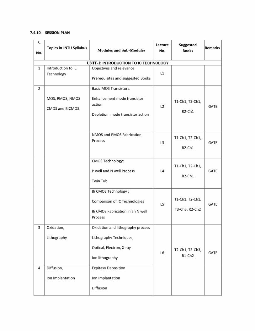
7.4.10 SESSION PLAN
S.
No. Topics in JNTU Syllabus
Modules and Sub-Modules
Lecture
No.
Suggested
Books Remarks
UNIT-I: INTRODUCTION TO IC TECHNOLOGY
1 Introduction to IC
Technology
Objectives and relevance
Prerequisites and suggested Books L1
2
MOS, PMOS, NMOS
CMOS and BICMOS
Basic MOS Transistors:
Enhancement mode transistor
action
Depletion mode transistor action
L2 T1-Ch1, T2-Ch1,
R2-Ch1 GATE
NMOS and PMOS Fabrication
Process
L3 T1-Ch1, T2-Ch1,
R2-Ch1 GATE
CMOS Technology:
P well and N well Process
Twin Tub
L4 T1-Ch1, T2-Ch1,
R2-Ch1 GATE
Bi CMOS Technology :
Comparison of IC Technologies
Bi CMOS Fabrication in an N well
Process
L5 T1-Ch1, T2-Ch1,
T3-Ch3, R2-Ch2 GATE
3 Oxidation,
Lithography
Oxidation and lithography process
Lithography Techniques;
Optical, Electron, X-ray
Ion lithography L6
T2-Ch1, T3-Ch3,
R1-Ch2
GATE
4 Diffusion,
Ion Implantation
Expitaxy Deposition
Ion Implantation
Diffusion
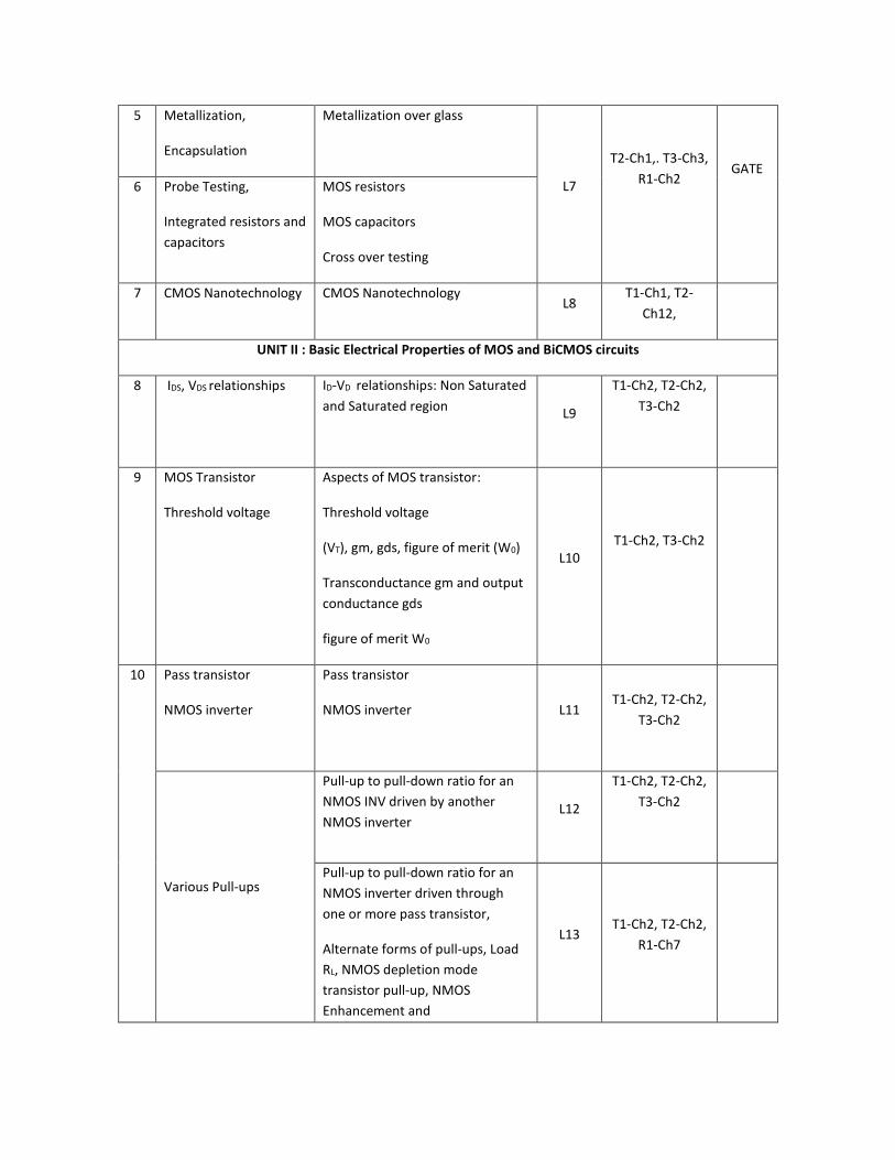
5 Metallization,
Encapsulation
Metallization over glass
L7
T2-Ch1,. T3-Ch3,
R1-Ch2
GATE
6 Probe Testing,
Integrated resistors and
capacitors
MOS resistors
MOS capacitors
Cross over testing
7 CMOS Nanotechnology CMOS Nanotechnology L8
T1-Ch1, T2-
Ch12,
UNIT II : Basic Electrical Properties of MOS and BiCMOS circuits
8 IDS, VDS relationships ID-VD relationships: Non Saturated
and Saturated region L9
T1-Ch2, T2-Ch2,
T3-Ch2
9 MOS Transistor
Threshold voltage
Aspects of MOS transistor:
Threshold voltage
(VT), gm, gds, figure of merit (W0)
Transconductance gm and output
conductance gds
figure of merit W0
L10 T1-Ch2, T3-Ch2
10
Pass transistor
NMOS inverter
Pass transistor
NMOS inverter
L11 T1-Ch2, T2-Ch2,
T3-Ch2
Various Pull-ups
Pull-up to pull-down ratio for an
NMOS INV driven by another
NMOS inverter L12
T1-Ch2, T2-Ch2,
T3-Ch2
Pull-up to pull-down ratio for an
NMOS inverter driven through
one or more pass transistor,
Alternate forms of pull-ups, Load
RL, NMOS depletion mode
transistor pull-up, NMOS
Enhancement and
L13 T1-Ch2, T2-Ch2,
R1-Ch7
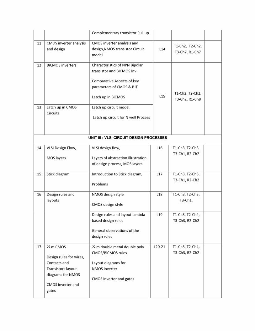
Complementary transistor Pull up
11 CMOS inverter analysis
and design
CMOS inverter analysis and
design,NMOS transistor Circuit
model
L14 T1-Ch2, T2-Ch2,
T3-Ch7, R1-Ch7
12 BiCMOS inverters Characteristics of NPN Bipolar
transistor and BICMOS Inv
Comparative Aspects of key
parameters of CMOS & BJT
Latch up in BiCMOS L15 T1-Ch2, T2-Ch2,
T3-Ch2, R1-Ch8
13 Latch up in CMOS
Circuits
Latch up circuit model,
Latch up circuit for N well Process
UNIT III : VLSI CIRCUIT DESIGN PROCESSES
14 VLSI Design Flow,
MOS layers
VLSI design flow,
Layers of abstraction Illustration
of design process, MOS layers
L16 T1-Ch3, T2-Ch3,
T3-Ch1, R2-Ch2
15 Stick diagram Introduction to Stick diagram,
Problems
L17 T1-Ch3, T2-Ch3,
T3-Ch1, R2-Ch2
16 Design rules and
layouts
NMOS design style
CMOS design style
L18 T1-Ch3, T2-Ch3,
T3-Ch1,
Design rules and layout lambda
based design rules
General observations of the
design rules
L19 T1-Ch3, T2-Ch4,
T3-Ch3, R2-Ch2
17 2m CMOS
Design rules for wires,
Contacts and
Transistors layout
diagrams for NMOS
CMOS inverter and
gates
2m double metal double poly
CMOS/BiCMOS rules
Layout diagrams for
NMOS inverter
CMOS inverter and gates
L20-21 T1-Ch3, T2-Ch4,
T3-Ch3, R2-Ch2

18 Scaling of MOS circuits Scaling models and scaling
factors
Scaling factors for device
parameters
L22 T1-Ch5, T2-Ch4,
T3-Ch4, R2-Ch2
UNIT IV: GATE LEVEL DESIGN
19 Logic gates and other
complex gates
CMOS implementation and
Layouts of:
NAND, NOR, AND, OR, NOT and
EX-OR gates
L24-25 T1-Ch6,
T2-Ch5, R2-Ch3
20 Switch logic,
Alternate gate circuits
Switch logic
Alternate gate circuits
Pseudo NMOS logic
L26 T1-Ch6,
T2-Ch5, R2-Ch3
DCVS logic
Domino logic
L27 T1-Ch6,
T2-Ch5, R2-Ch3
21 Time delays, Driving
Large Capacitive loads
Area capacitance of layer
standard unit of capacitance,
Calculations of Delay unit()
Methodology for drive large
capacitive loads
L28 T1-Ch4,
T2-Ch5, T3-Ch4,
R2-Ch4
22 Wiring Capacitance,
Fan-in, Fan-out,
Choice of Layers
Wiring Capacitance,
Fan-in, Fan-out,
Choice of Layers
L29 T1-Ch4, T2-Ch5,
T3-Ch4, R2-Ch4
UNIT V: DATA PATH SUBSYSTEM DESIGN
23 Shifters Combinational shifters L30 T1-Ch8, T2-Ch7,
T3-Ch8,
R1-Ch11,
R2-Ch6
24 Adders Full adder
parallel adder
serial adder
Carry-save addition
Transmission –gate adder
L31
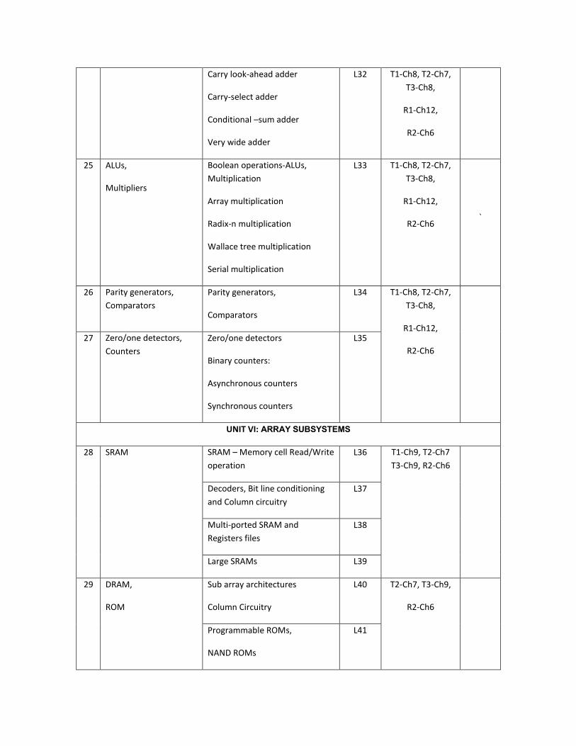
Carry look-ahead adder
Carry-select adder
Conditional –sum adder
Very wide adder
L32 T1-Ch8, T2-Ch7,
T3-Ch8,
R1-Ch12,
R2-Ch6
25 ALUs,
Multipliers
Boolean operations-ALUs,
Multiplication
Array multiplication
Radix-n multiplication
Wallace tree multiplication
Serial multiplication
L33 T1-Ch8, T2-Ch7,
T3-Ch8,
R1-Ch12,
R2-Ch6
`
26 Parity generators,
Comparators
Parity generators,
Comparators
L34 T1-Ch8, T2-Ch7,
T3-Ch8,
R1-Ch12,
R2-Ch6 27 Zero/one detectors,
Counters
Zero/one detectors
Binary counters:
Asynchronous counters
Synchronous counters
L35
UNIT VI: ARRAY SUBSYSTEMS
28 SRAM SRAM – Memory cell Read/Write
operation
L36 T1-Ch9, T2-Ch7
T3-Ch9, R2-Ch6
Decoders, Bit line conditioning
and Column circuitry
L37
Multi-ported SRAM and
Registers files
L38
Large SRAMs L39
29 DRAM,
ROM
Sub array architectures
Column Circuitry
L40 T2-Ch7, T3-Ch9,
R2-Ch6
Programmable ROMs,
NAND ROMs
L41
30 Serial Access Memories Shift Registers L42 T3-Ch9
31 Content Addressable
Memory
Queues (FIFO, LIFO) L43
Content Addressable memory L44
UNIT VII: SEMICONDUCTOR INTEGRATED CIRCUIT DESIGN
32 PLAs, FPGAs,
CPLDs
Introduction to Programmable
Logic arrays,
Field programmable gated arrays,
Complex programmable logic
devices
L45-46
T1-Apendix-C, T2-
Ch6,
R1-Ch13,
R2-Ch6
33 Standard cells Standard –cell based ASICs L47
34 Programmable Array
Logic
Logic functions Implementation
using PLAs
L 48-49 T1-Apendix-C, T2-
Ch6
R1-Ch13
35 Design approach Design approach for different
target devices
L50 T2-Ch6, T3-Ch10
36 Parameters influencing
Low Power Design
Approach for Low power design L51 T2-Ch6, T3-Ch6,
R2-Ch3
UNIT VIII: CMOS TESTING
37 CMOS Testing,
Need for testing
Functionality Test
Manufacturing Test
L52 T1-Ch10, T2-Ch9,
T3-Ch12, R2-Ch10
38 Test principles Fault models
Observability and controllability
Fault coverage ATPG
L53 T1-Ch10, T2-Ch9,
T3-Ch12, R2-Ch10
Delay fault testing
Statistical fault analysis etc.
L54 T1-Ch10, T2-Ch9,
T3-Ch12, R2-Ch10
39 Design strategies for
test
Design for testability
Adhoc Testing
Scan based test techniques
L55 T1-Ch10, T2-Ch9,
T3-Ch12, R2-Ch10

Self test techniques
IDDQ testing
L56 T1-Ch10, T2-Ch9,
T3-Ch12, R2-Ch10
40 Chip level test
techniques
Regular logic arrays
Memories, Random logic
L57 T1-Ch10, T2-Ch9,
T3-Ch12, R2-Ch10
41 System level test
techniques
Boundary scan,
The Test Access Port (TAP)
L58 T1-Ch10, T2-Ch9,
T3-Ch12, R2-Ch10
42 Layout design for
improved testability
Layout design for improved
testability
L59 T1-Ch10, T2-Ch9,
T3-Ch12, R2-Ch10
7.4.11 STUDENT SEMINAR TOPICS
1. “3 D Circuits”, C.Y Kuo, C.J.Shihond and K.Chakrabarty, IEEE Transcations on VLSI
System, Vol.22,No. 03,Page No. 665,Mar 2014.
2. “Sequential Circuits using Carbon Nano tubes”, Journal of VLSI Design Tools & Tech., Sep-
Dec 2013,STM Journal.
3. “Fault tolerant design of digital system”, Fault tolerant and fault testable hardware
design, P.K.Lal.
4. “Fabrication of CMOS using Silicon on insulator”, Principles of CMOS VLSI
Design,Neil Weste, and Eshraghian, Pearson Education, 1999
5. “Over view on Programmable Logic Devices” ,VLSI Designing K. Lal Kishore, VSV
Prabhakar IK International, 2009.
7.4.12 QUESTION BANK
UNIT – I
1. Explain the fabrication of a CMOS transistor. (Nov 13)
2. With neat sketches explain how npn transistor is fabricated in Bipolar process.
(Nov/Dec 13, May 09,Sep 08, 06)
3. With neat diagrams, explain the different steps in p-well fabrication of CMOS transistors.
(Nov 12)
4. i.Give the steps of nMOS fabrication along with neat diagrams.
ii.What are the thermal apsects of processing nMOS and CMOS devices?
iii.Draw a twin tub structure and explain. (Nov 12)
5. How Integrated Passive Components are fabricated in ICs? Explain.(Jan 11,May 09)
6. Explain about oxidation, Diffusion and Ion Implementation Processes of I C
Fabrication. (Jan 11)
7. i.With the help of neat sketches, explain about the fabrication sequence of I.C.
ii.Using necessary sketches, explain about photolithography process, in semi conductor
device manufacture. (Jan 11 May 09,08, 07, Sep 06)
8. i.Clearly explain the diffusion process in IC fabrication.
ii.Clearly explain various diffusion effects in silicon with emphasis on VLSI application.
(May 09,Sep 07)
9. Explain the MOS Transistor operation with the help of neat sketches in the following
modes
i. Enhancement mode
ii. Depletion mode (May 09)
10. i. With neat sketches explain the NMOS and PMOS fabrication procedure.
ii. Draw the cross sectional view of CMOS P - Well inverter. (May 09)
11. i.With neat sketches explain automatic diffusion mechanism
ii.Explain clearly about different types of packing methods used in IC fabrication
(Sep 08) 12. Explain about the following two oxidation methods
i. High pressure oxidation
ii. Plasma oxidation (Sep 08, May 07)
13. i. With neat sketches explain CMOS fabrication using n-well process.
ii. Explain how capacitors are fabricated in CMOS process. (Sep 08,07)
14. Mention different growth technologies of the thin oxides and explain about any one
technique. (Sep 08)
15. i. Mention the properties of the twin oxide.
ii. Clearly explain about ION implantation step in IC fabrication
16. With neat sketches explain the electron lithography process.
(May 08, Sep, May 06, May 05)
17. Compare between CMOS and bipolar technologies. (May 08, 05)
18. i. What are the steps involved in the n MOS fabrication - Explain with neat sketches
ii. In what way pMOS fabrication is different from nMOS fabrication?
(May 08, Nov 03)
19. i. What is Moore’s Law? Explain its relevance with respect to evolution of IC
technology.
ii. What is the size of Silicon wafer currently used for the manufacture of ICS?
iii. What is the current commercial device feature size? (May 08, 03)
20. With neat sketches explain how Diodes and Resistors are fabricated in Bipolar process.
(May 08, Sep 07)
21 i. With neat sketches explain how resistors and capacitors are fabricated in p-well process.
ii. With neat sketches explain how resistors and capacitors are fabricated in n-well process.
(May 08, Sep, May 07)
22. Explain the following
i. Thermal oxidation technique.
ii. Kinetics of thermal oxidation. (May 08)
23. Explain the following
i. Double metal MOS process rules.
ii. Desing rules for P-well CMOS process (May 08)
24. With neat sketches explain CMOS fabrication using Twin - Tub process. (May 08)
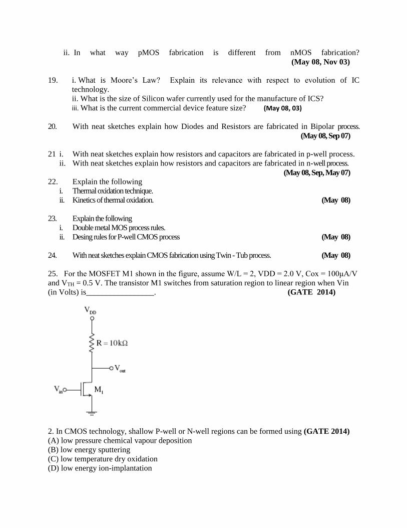
25. For the MOSFET M1 shown in the figure, assume W/L = 2, VDD = 2.0 V, Cox = 100μA/V
and VTH = 0.5 V. The transistor M1 switches from saturation region to linear region when Vin
(in Volts) is_________________. (GATE 2014)
2. In CMOS technology, shallow P-well or N-well regions can be formed using (GATE 2014)
(A) low pressure chemical vapour deposition
(B) low energy sputtering
(C) low temperature dry oxidation
(D) low energy ion-implantation

3. The output (Y) of the circuit shown in the figure is (GATE 2014)
(A) A + B+ C
(B) A + B . C + A .C
(C) A + B+ C
(D) A . B . C
4. In MOSFET fabrication, the channel length is defined during the process of
( GATE 2014)
(A) Isolation oxide growth
(B) Channel stop implantation
(C) Poly-silicon gate patterning
(D) Lithography step leading to the contact pads
5. In IC technology, dry oxidation (using dry oxygen) as compared to wet oxidation(using steam
or water vapor) produces (GATE2013)
(A) superior quality oxide with a higher growth rate
(B) inferior quality oxide with a higher growth rate
(C) inferior quality oxide with a lower growth rate
(D) superior quality oxide with a lower growth rate
6. In a MOSFET operating in the saturation region, the channel length modulation
effect causes (GATE2013)
(A) an increase in the gate-source capacitance
(B) a decrease in the Transconductance
(C) a decrease in the unity-gain cutoff frequency
(D) a decrease in the output resistance
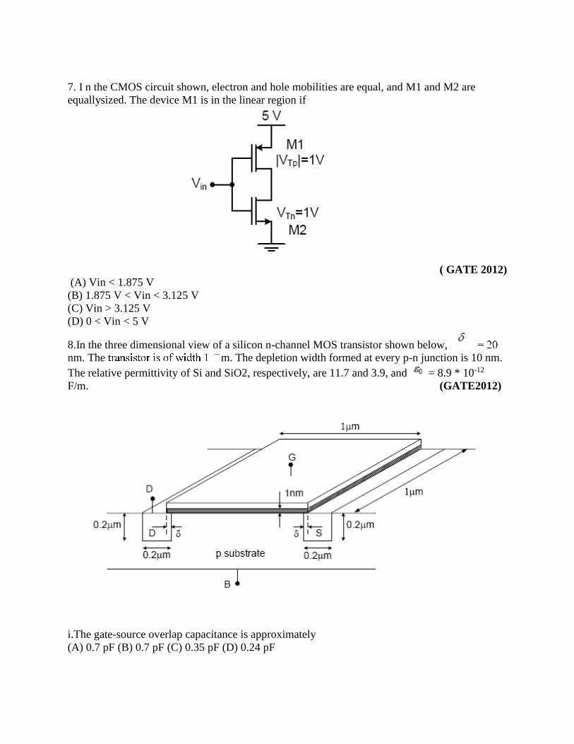
7. I n the CMOS circuit shown, electron and hole mobilities are equal, and M1 and M2 are
equallysized. The device M1 is in the linear region if
( GATE 2012)
(A) Vin < 1.875 V
(B) 1.875 V < Vin < 3.125 V
(C) Vin > 3.125 V
(D) 0 < Vin < 5 V
8.In the three dimensional view of a silicon n-channel MOS transistor shown below,
nm. The m. The depletion width formed at every p-n junction is 10 nm.
The relative permittivity of Si and SiO2, respectively, are 11.7 and 3.9, and = 8.9 * 10-12
F/m. (GATE2012)
i.The gate-source overlap capacitance is approximately
(A) 0.7 pF (B) 0.7 pF (C) 0.35 pF (D) 0.24 pF
ii. The source-body junction capacitance is approximately
(A) 2 pF (B) 7 pF (C) 2 pF (D) 7 pF
9. Thin gate oxide in a CMOS process in preferably grown using
(GATE 2010)
(A) wet oxidation (B) dry oxidation
(C) epitaxial deposition (D) ion implantation
UNIT – II
1. Derive the equation for the drain current of a NMOS transistor. (May 13)
2 i. Derive the expression for the threshold voltage of MOSFET.
ii. Explain the latch-up phenomenon in CMOS circuits and the methods by which that can
be eliminated.
(Nov/Dec 12) 3. i. What is meant by figure of Merit of a transistor? Derive the figure of merit of MOS
transistor.
ii. Give a comparison between CMOS and Bipolar transistor with respect to their(May 12)
4. Draw the circuit for NMOS inverter and explain its operation. (Jan 11)
5. Draw the circuits for n-MOS, p-MOS and C-MOS Inverter and explain about their
operation and compare them. (Jan 11)
6. Explain about the following terms, using necessary theoretical equations, pertaining to
MOSFETs.
i. Threshold voltage VTh and its effect on MOSFET current Equations
ii. Body effect parameter. (Jan 11, Sep, May 08, Sep, May 07))
7. i. Draw an n MOS transistor model indicating all parameters.
ii. Draw the circuit diagram of a Bi CMOS inverter with no static current.
iii. What is latch up incase of CMOS circuits? Explain with relevant diagrams. How latch
up problem can be overcome? (May 09, 08, 04)
8. i. Explain the operation of BiCMOS inverter? Clearly specify its characteritics.
ii. Explain how the BiCMOS inverter performance can be improved. (May 09,08)
9. i. With neat sketches explain the drain characteristics of an n-channel enhancement
MOSFET.
ii. An-MOS Transistor is operated in the Active region with the following parameters VGS
= 3.9V; Vtn = 1V; W/L = 100; µnCox = 90 µA/V2
Find its drain current and drain source resistance. (May 09,Sep 07)
10. i. What are the different forms of pull ups?
ii. Determine the pull up to pull down ratio of an n MOS inverter driven by another n MOS
transistor.
(May 09, 04)
11. i.Explain with neat sketches the Drain and Transfer characteristics of n-channel
enhancement MOSFET.
ii. With neat sketches explain the transfer characteristics of a CMOS inverter. (May 09)
12. i. Derive an equation for Tran conductance of an n channel enhancement MOSFET operating in active
region.
ii. A PMOS transistor is operated in triode region with the following parameters. VGS=- 4.5V, Vtp= -1V;
VDS=-2.2 V, (W/L) =95, µnCox =95 A/V 2. Find its drain current and drain source resistance.(May 09)
13. i. With neat sketches explain the formation of the inversion layer in P-channel
Enhancement MOSFET.
ii. An NMOS Transistors is operated in the triode region with the following parameters
VGS = 4V; Vtn = 1V; VDS = 2V ; W/L = 100; µnCox = 90 A/V 2 Find its drain current
and drain source resistance.
(May 09)
14. i. Explain nMOS inverter and latch up in CMOS circuits.
ii. Draw the nMOS transistor circuit model and explain various components of the model. (May 08)
15. i. Explain various regions of CMOS inverter transfer characteristics.
ii. For a CMOS inverter, calculate the shift in the transfer characteristic curve when ratio is varied
from 1/1 to 10/1 (May 08)
UNIT – III
1. i. Explain the VLSI Design flow.
ii. What is a stick diagram? Draw the stick diagram of a three input CMOS NAND
gate. (Nov 13)
2. i. What are lambda based design rules? Explain design rules for wires and MOS
transistors.
ii. Explain difference between stick diagram and Layout. Draw layout of two input
XOR logic by showing all the layers. (Nov/Dec 13)
3. i. Explain the color code used for drawing stick diagram for NMOS and PMOS designs.
n
p

ii. What are the different types of contact cuts made during the fabrication of an IC?
iii. Draw the stick diagram for CMOS inverter. (Nov/Dec 12)
4 i. Explain Lambda -based design rules with neat figures.
ii. Draw a stick diagram and mask layout of 8:1 nMOS inverter circuit. Both Input and
output points should be Poly silicon layer. (May 12)
5. i. Explain about rules for drawing Stick's Diagram.
ii. Draw the circuit for 2-input NAND gate and draw the layout diagram for the same,
giving explanation.
(Jan 11)
6. i. Explain about the Stick notation and rules for Stick Diagram.
ii. Draw the circuit for 2-input NOR gate and its Stick Diagram, giving explanations.
(Jan 11)
7. Explain about the notations used to draw the stick diagram. Draw the Stick's diagram for
NMOS Inverter give brief explanation. (Jan 11)
8 i. What is stick diagram? Draw the stick diagram and layout for a CMOS inverter.
ii. What are the effects of scaling on Vt?
iii. What are design rules? Why is metal-metal spacing larger than poly-poly spacing.
(May 09, 08)
9. Design a stick diagram for the PMOS logic shown below Y=(AB + CD)’ (May 09, 08)
10. Two nMOS inverters are cascaded to drive a capacitive load CL=14Cg .Calculate the
pair delay Vin to Vout in terms of for the given data. Inverter -A: LP.U= 12 , WP.U
= 4 , LP.d = 1, WP.d = 1 , Inverter -B: LP.U= 4 , WP.U = 4 , LP.d = 2 , WP.d = 8.
(May 09,06)
11. Design stick diagram and layout for two input CMOS NAND gate indicating all the
regions & layers.
(May 09) 12. i. Discuss design rule for wires (orbit 2µ CMOS).
ii. Discuss the transistor related design rule (orbit 2 µ CMOS). (May 09)
13. Design a stick diagram for CMOS -Ex-OR gate. (May 09)
14. Design a layout diagram for the CMOS logic shown below. Y=(A+B+C)’ (May 09)
15. Design a layout diagram for the NMOS logic shown below Y= [(A+B)C]’ (Sep,May 08)
16. What is a stick diagram and explain about different symbols used for components in stick diagram.
(Sep 08, May 07)
17. Design a layout diagram for pMOS inverter (Sep 08)
18. Design a layout diagram for two input CMOS NOR gate. (Sep, May 08, May 07)
19. Design a stick diagram for n-MOS Ex-OR gate. (Sep 08, Sep, May 07)
20. Design a stick diagram for two input p-MOS NAND and NOR gates. (Sep 08, 06, May 07)
21. Design a layout diagram for CMOS inverter. (May 08, Sep, May 07)
22. Design a stick diagram for two input n-MOS NAND and NOR gates. (May 08, 06)
23. Draw the stick diagram and a translated mask layout for nMOS inverter circuit.(May 08)
24. Draw the stick diagram and mask layout for a CMOS two input NOR gate and stick
diagram of two input NAND gate. (May 08)
UNIT IV
1. What is the problem encountered by VLSI circuits in driving large capacitive
Loads? Suggest and explain two solutions to overcome the problem. (Nov 13)
2. i. Implement the function F = ab +c (a+b) using CMOS logic.
ii. What is the effect of delay on driving large capacitive loads?
iii. Define Logical Effort. Obtain the logical effort of three input NOR gate (Nov/Dec 13)
3. i. What are the issues that happen when large capacitive loads are to be driven?
How they are overcome?
ii. Derive the expression for CMOS inverter rise time and fall time (Nov/Dec 12,May 09)
4. i. Draw the logic circuit for Inverter with a transmission gate to provide tri-state output, and
explain the same.
ii. Explain about Pass Transistor Logic, with examples. (Jan 11)
5. i. Derive the expressions for Rise-Time R and fall time f in the case of CMOS Inverter.
ii. Express the Area capacitance in terms of standard capacitance units. (Jan 11)
6. Explain about Gate level verification and timing Reports pertaining to VLSI Design.
(Jan 11)
7. Explain clearly about different parasitic capacitances of an n MOS transistor.(May09, 05)
8. Describe the following briefly
i. Cascaded inverters as drivers.
ii. Super buffers.
iii. BiCMOS drivers. (May 09)
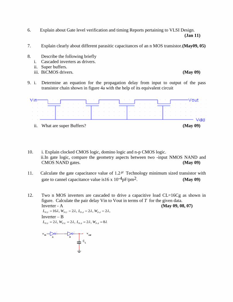
9. i. Determine an equation for the propagation delay from input to output of the pass
transistor chain shown in figure 4a with the help of its equivalent circuit
ii. What are super Buffers? (May 09)
10. i. Explain clocked CMOS logic, domino logic and n-p CMOS logic.
ii.In gate logic, compare the geometry aspects between two -input NMOS NAND and
CMOS NAND gates. (May 09)
11. Calculate the gate capacitance value of 1.2 Technology minimum sized transistor with
gate to cannel capacitance value is16 x 10-4pF/pm2. (May 09)
12. Two n MOS inverters are cascaded to drive a capacitive load CL=16Cg as shown in
figure. Calculate the pair delay Vin to Vout in terms of T for the given data.
Inverter - A (May 09, 08, 07)
Inverter – B
. . . .16 , 2 , 2 , 2 ,P U P U P d P dL W L W
. . . .2 , 2 , 2 , 8P U P U P d P dL W L W
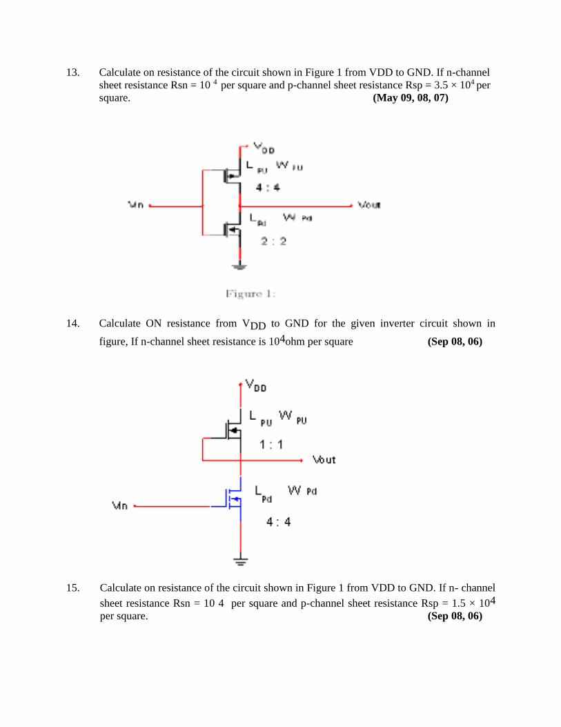
13. Calculate on resistance of the circuit shown in Figure 1 from VDD to GND. If n-channel
sheet resistance Rsn = 10 4 per square and p-channel sheet resistance Rsp = 3.5 × 10⁴ per
square. (May 09, 08, 07)
14. Calculate ON resistance from VDD to GND for the given inverter circuit shown in
figure, If n-channel sheet resistance is 104ohm per square (Sep 08, 06)
15. Calculate on resistance of the circuit shown in Figure 1 from VDD to GND. If n- channel
sheet resistance Rsn = 10 4 per square and p-channel sheet resistance Rsp = 1.5 × 10⁴
per square. (Sep 08, 06)
16. Explain the delay calculation procedure for CMOS inverter. (May 08, 05)
17. Describe three sources of wiring capacitances. Explain the effect of wiring capacitance
on the performance of a VLSI circuit. (May 08)
18. i. Define and explain the following
a. Sheet resistance concept applied to MOS transistors and inverters.
b. Standard unit of capacitance.
ii. Explain the requirement and functioning of a delay unit. (May 08)
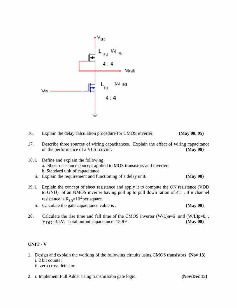
19. i. Explain the concept of sheet resistance and apply it to compute the ON resistance (VDD
to GND) of an NMOS inverter having pull up to pull down ration of 4:1 , If n channel
resistance is Rsn=104per square.
ii. Calculate the gate capacitance value is . (May 08)
20. Calculate the rise time and fall time of the CMOS inverter (W/L)n=6 and (W/L)p=8, ,
VDD=3.3V. Total output capacitance=150fF (May 08)
UNIT - V
1. Design and explain the working of the following circuits using CMOS transistors (Nov 13)
i. 2 bit counter
ii. zero cross detector
2. i. Implement Full Adder using transmission gate logic. (Nov/Dec 13)
ii. Draw and explain parity generator block diagram and stick diagram.
3. With neat circuit diagram, explain the operation of
i. Carry look ahead adder
ii. Barrel shifter. (Nov/Dec 12)
4. i. Design a parity generator by first designing one bit cell.
ii. What is two phase clocking? How does it help in designing sequential circuits?(May 12)
5. i. Set out the mask layout for a 4 way MUX using transmission gate switches.
ii. Use the above design as a block and draw a 4 bit shift Left/ Right shifter sub system.
(May 12)
6 Implement ALU functions with Adder. (May 12)
7. What are the circuit design considerations in the case of static adder circuits. (Jan 11)
8 i. Explain about bit sliced Data path organization. What is the significance of Data paths in
digital processors?
ii. Give the Truth Table for full adder and explain its Boolean expression. (Jan 11)
9. Draw the circuit for Transmission -gate-based full adder with sum and carry delays of
same value and explain its working. (Jan 11)
10. Explain briefly the CMOS system design based on the data path operators, memory
elements, control structures and I/O cells with suitable examples. (May 09)
11. Explain how a Booth recoded multiplier reduces the number of adders. (May 09)
12. i. Design a magnitude comparator based on the data path operators.
ii. Draw the Schematic and mask layout of array adder used in Booth Multiplier and explain
the principle of multiplication in Booth Multiplier. (May 09)
13. i. Explain the CMOS system design based on the data path operators with a suitable
example.
ii. Draw and explain the basic Memory- chip architecture. (May 09,08)
14. i. Draw the schematic for tiny XOR gate and explain its operation.
ii. Draw the circuit diagram for 4-by-4 barrel shifter using complementary transmission
gates and explain its shifting operation. (May 08)
UNIT –VI
1. i. Explain the working of a SRAM cell.
ii. Explain the working principle of content addressable memory. (Nov 13)
2. With relevant circuit diagram, explain the operation of
i. DRAM cell
ii. Content Addressable Memory (Nov/Dec 12)
3. i. Draw the circuit for 4 transistor SRAM and explain its working.
ii. Draw the one cell dynamic RAM circuit and explain its working. (Jan 11)
4. i. Explain the principle of Gate Arrays.
ii. With the help of sketches explain how NAND gate can be realized using CMOS gate
Arrays. (Jan 11)
5. How many ROM bits are required to build a 16-bit adder/subtractor with mode control,
carry input, carry output and two’s complement overflow output. Show the block
schematic with all inputs and outputs? (Jan 10, Mar 06, Nov 05)
6. Design an 8x4 diode ROM using 74x138 for the following data starting from the first
location? B,2,4,F,A,D,F,E (Jan 10, Nov 05)
7. Draw the internal structure of synchronous SRAM and explain the operation?
(Nov 09, Mar 06, May 05)
8. Explain how a 4×4 binary multiplier can be designed using 256x8 ROM. (Nov 09, 08)
9. i. How many number of address lines are required to access all the locations of a 256K x 8
memory? What is the data word size stored in this memory?
ii. What are synchronous SRAMs? Describe how synchronous operations are performed in
SSRAM with the help of its internal block diagram showing the inputs and outputs.
(Nov 09)
10. With the help of internal structure of a small SRAM and its timing diagram, describe
Read and write operations performed in the SRAM. (Nov 09)
11. i. Build a layout for a 32K x 8 ROM using suitable basic building blocks, like, decoders
and multiplexers.
ii. Discuss the concept along with the merits of two-dimensional decoding for a Read Only
Memory. (Nov 09)
12. i. With the help of internal structure and timing diagram of a typical ROM with active low
chip select and output enable signals, describe timing criteria of a ROM to be configured
either in normal or power down modes.
ii. List out the advantages and disadvantages of Read only memories based on
combinational circuit design. (Nov 09)
13. i. Draw and explain the internal structure of synchronous SRAM
ii. Explain the design procedure of 4x4 binary multiplexer using 256 x 8 ROM (Nov 09)
14. i. Discuss how PROM, EPROM and EEPROM technologies differ from each other?
ii. With the help of timing waveforms, explain read and write operations of SRAM.
(Nov 08)
15. Realize the logic function performed by 74×381 with ROM. (Nov 08)
16. i. How many ROM bits are required to build a 16-bit adder/subtractor with mode control,
carry input, carry output and twos complement overflow output? Show the block
schematic with all inputs and outputs?
ii. Design an 8×4 diode ROM using 74X138 for the following data starting from the first
location (Nov 08)
17. i. Design an 8x4 diode ROM using 74x138 for the following data starting from the first
location? 1,4,9,B,A,0,F,C (Feb 08, Nov 07Mar 06)
ii. Draw the internal structure of synchronous SRAM and explain its operation?
(Feb 08,07,Nov 07,04)
18. Design an 8x8 diode ROM using 74x 138 for the following data starting from the first
location.
11, 22, 33, FF, DD,CC, 01, 7E (Feb 08)
19. Realize the logic function performed by 74x381 with ROM?
(Feb 08, 07, Nov 06, Mar 06)
20. Explain the internal structure of 64K x 1 DRAM? With the help of timing waveforms
discuss DRAM access? (Feb 08,07, Nov 07,06, 05 Mar 06, Nov 05, May 05)
21. With the help of timing waveforms, explain read and write operations of static SRAM?
(Feb 08, Nov 07, 06, 04)
22. Explain the necessity of two dimensional decoding mechanism in memories? Draw
MOS transistor memory cell in ROM and explain the operation? (Feb 08, Nov07, 04)
UNIT –VII
1. i. Explain the parameters affecting the power dissipation of a circuit
ii. Write short notes on CPLDs. (Nov 13)
2. i. What is FPGA? Draw and explain basic structure of FPGA.
ii. Implement the following functions using PAL (Nov/Dec 13)
f (a,b,c,d) = ab + bc
f (a,b,c,d) = ab + cd
f (a,b,c,d) = ba + cd
3. i. Differentiate between PROM, PAL and PLA.
ii. Implement a 3 bit synchronous counter using PAL. (Nov/Dec 12)
4. Write a short note on
i. Hardware / Software co design.
ii. Timing analysis in chip design flow. (May 12)
5. Using block diagrams and schematics explain about Configurable Logic Blocks(CLBs).
(Jan 11)
6. Explain about the principle, operation, salient features and applications of FPGAs
(Jan 11)
7. With neat sketch clearly explain the architecture of a PAL.
(May 09,Sep, May 08, 06, 05)
8. i. What are the advantages and disadvantages of the reconfiguration.
ii. Mention different advantages of Anti fuse Technology. (May 09, Sep 08, 06)
9. i. What are the characteristics of 22V10 PAL CMOS device and draw its I/O structure.
ii. Explain any one chip architecture that used the anti fuse and give its advantages.
(May 09,08)
10. i. Draw and explain the FPGA chip architecture.
ii. Draw and explain the AND/NOR representation of PLA (May 09)
11. i. Draw the typical architecture of PAL and explain the operation of it.
ii. What is CPLD? Draw its basic structure and give its applications. (May 09)
12. Write briefly about:
i. Channelled gate arrays
ii. Channelless gate arrays with neat sketches. (May 09)
13. i. Explain the methods of programming of PAL CMOS device.
ii. Draw and explain the architecture of an FPGA . (May 09, 08)
14. Implement Full-adder circuit using PAL. (May 09, 08)
15. What are the different inputs that are provided to the place and route tool and explain the
significance of each input (Sep 08)
16. Clearly explain each step of high level design flow of an ASIC. (Sep 07,08, May 07)
17. Explain the following process in the ASIC design flow. (May 08, Sep 07)
i. Functional gate level verification.
ii. Static timing analysis

18. i. Draw the typical standard-cell structure showing low-power cell and explain it.
ii. Sketch a diagram for two input XOR using PLA and explain its operation with the help of
truth table.
(May 08) 19. i. Explain the function of 4:1 Mux in PAL CMOS device with the help of I/O structure.
ii. Explain how the pass transistors are used to connect wire segments for the purpose of
FPGA programming.
(May 08) 20. Clearly discus about the following FPGA Technology
i. Anti fuse Technology
ii. Static RAM Technology (May 08)
UNIT VIII
1. Discuss a technique of testing a VLSI circuit under these levels (Nov 13)
i. system level
ii. chip level
2.i. What are the different types of faults that occur in manufacturing of chips?
Explain with an example.
ii. What is BILBO? Draw the logic diagram of BILBO and explain its operation in
different modes. (Nov/Dec 13)
3. i. Explain the need for testing.
ii. Discuss any two system techniques used for system level testing. (Nov/Dec 12)
4 i. Explain about:
i.. Diagnostic Test
ii. Functional Test
iii. Parametric Test.
ii. Explain about Design strategies for Testing. (Jan 11)
5. Explain about static Timing and Post Layout Timing. (Jan 11)
6. i. What are the different categories of DFT techniques? Explain.
ii. What is meant by signature analysis in Testing? Explain with an example. (Jan 11)
7. Write notes on any TWO
i. DGT
ii. BIST
iii. Boundary scan Testing. (Jan 11)
8. i. Draw the basic structure of parallel scan and explain how it reduces the long scan chains.
ii. Draw the state diagram of TAP Controller and explain how it provides the control signals
for test data and instruction register. (May 09, 08)
9. i. What is ATPG? Explain a method of generation of test vector
ii. Explain the terms controllability, observability and fault coverage. (May 09)
10. i. Explain the gate level and function level of testing.
ii. A sequential circuit with in? inputs and ‘m’ storage devices. To test this circuit how many
test vectors are required.
iii. What is sequential fault grading? Explain how it is analyzed. (May 09)
11. i. Define the term DFT and explain about it.
ii. Explain any one test procedure to test sequential logic. (May 09)
12. i. Explain how an improved layout can be reduced faults in CMOS circuits.
ii. Explain how a pseudo random sequence generator may be used to test a 16-bit data path.
How the outputs would be collected and checked. (May 08)
13. i. Compare functionality test and manufacturing test.
ii. What type of testing techniques are suitable for the following:
a. Memories
b. Random logic
c. Data path.
iii. How IDDQ testing is used to test the bridge faults? (May 08)
7.4.12 ASSIGNMENT QUESTIONS
UNIT I
1. Explain the MOS Transistor operation with the help of neat sketches in the following modes
i. Enhancement mode
ii. Depletion mode
2. With neat sketches explain the NMOS and PMOS fabrication procedure
3. Explain the fabrication of a CMOS transistor using N well, P well and twin tub .
4. With neat sketches explain how npn transistor is fabricated in Bipolar process.
5. Explain about oxidation, Diffusion and Ion Implementation Processes of I C Fabrication.
UNIT II
1. Derive a relationship between Ids and Vdsof an NMOS transistor structure.

2. Explain the latch-up phenomenon in CMOS circuits and the methods by which that can
be eliminated.
3. Draw the circuits for n-MOS, p-MOS and C-MOS Inverter and explain about their
operation and compare them.
4. What are the different forms of pull ups?
5. Determine the pull up to pull down ratio of an n MOS inverter driven by another n MOS
transistor.
UNIT III
1. Explain the VLSI Design flow.
2. Explain Lambda -based design rules with neat figures.
3. Explain difference between stick diagram and Layout. Draw layout of two input
XOR logic by showing all the layers.
4. Draw a stick diagram and mask layout of 8:1 n MOS inverter circuit. Both Input and
output points should be Poly silicon layer.
5. Design a layout diagram for the CMOS logic shown below. Y=(A+B+C)’
UNIT IV
1. Derive the expression for CMOS inverter rise time and fall time.
2. What is the problem encountered by VLSI circuits in driving large capacitive
Loads? Suggest and explain two solutions to overcome the problem.
3. Describe the following briefly
i. Cascaded inverters as drivers.
ii. Super buffers.
iii. Bi CMOS drivers
4. Explain clocked CMOS logic, domino logic and n-p CMOS logic.
5. i. Draw the logic circuit for Inverter with a transmission gate to provide tri-state output, and
explain the same.
ii. Explain about Pass Transistor Logic, with examples
UNIT V
1. Implement Full Adder using transmission gate logic.
2. Design a parity generator by first designing one bit cell.
3. What is two phase clocking? How does it help in designing sequential circuits.
4. Design and explain the working of the following circuits using CMOS transistors
i. 2 bit counter
ii. zero cross detector
5. With neat circuit diagram, explain the operation of
i.Carry look ahead adder
ii.Barrel shifter.
UNIT VI
1. Draw the circuit for 4 transistor SRAM and explain its working.
2. Draw the one cell dynamic RAM circuit and explain its working.
3. With relevant circuit diagram, explain the operation of Content Addressable Memory.
4. i. Discuss the concept along with the merits of two-dimensional decoding for a Read
Only Memory
ii. List out the advantages and disadvantages of Read only memories based on
combinational circuit design
5. Design an 8×4 diode ROM using 74X138 for the following data starting from the first
location.
UNIT VII
1. What is FPGA? Draw and explain basic structure of FPGA.
2. Implement the following functions using PAL
f (a,b,c,d) = ab + bc
f (a,b,c,d) = ab + cd
f (a,b,c,d) = ba + cd
3. Write briefly about:
i. Channelled gate arrays
ii. Channelless gate arrays with neat sketches.
4. Clearly discus about the following FPGA Technology
i.Anti fuse Technology
ii.Static RAM Technology
5. i. What is CPLD? Draw its basic structure and give its applications
ii Differentiate between PROM, PAL and PLA
UNIT VIII
1. Discuss few techniques for chip level testing.
2. What are the different types of faults that occur in manufacturing of chips?
Explain with an example.
3. What is meant by signature analysis in Testing? Explain with an example.
4. Discuss any two system techniques used for system level testing.
5. i.Explain the need for testing
ii Explain about Design strategies for Testing.