700 v coolmostm p7 - infineon technologies
TRANSCRIPT

Application Note Please read the Important Notice and Warnings at the end of this document Revision 1.1
www.infineon.com 2017-10-13
AN_201701_PL52_006
700 V CoolMOSTM P7
First 700 V CoolMOS™ MOSFET developed on 300 mm for low power
applications
About this document
Scope and purpose
Infineon is introducing its first 700 V high voltage MOSFET (Metal Oxide Semiconductor Field Effect Transistor)
solution developed and produced on 300 mm for low power applications. 700 V CoolMOS™ P7 offers a price competitive solution for consumer applications such as chargers and adapters in the power range from 10 W to
75 W. These power converters are typically based on flyback topologies. 700 V CoolMOSTM P7 is no longer a
multi purpose MOSFET as it has become known, it is now a tailored technology for flyback and DCM
(discontinuous current mode) PFC applications and must not be used in any half bridge or full bridge configuration in which hard commutation on a conducting body diode can occur. The portfolio includes
popular packages which are a direct replacement for existing MOSFETs, allowing improved performance while
offering lower prices in comparison to other technologies targeting this low power market. 700 V CoolMOS™ P7 is able to fit into several low power packages such as SOT-223 with the lowest RDS(on) available on the market. Furthermore, it will be included in Infineon newest package concept; the IPAK with an isolated lead standoff.
This application note provides an explanation of the new CoolMOSTM technology. The goal of this application
note is to describe all technical and technological benefits 700 V CoolMOS™ P7 can offer in comparison to older
technologies and competitor products. Furthermore, it will present the evaluation of a customer charger to show the performance that can be achieved with 700 V CoolMOS™ P7 with respect to thermal performance, efficiency and electromagnetic interference behavior.
700 V CoolMOSTM P7 is the right solution for all the main challenges every designer of low power applications is facing, keeping BOM costs low while not sacrificing technical specifications and meeting safety requirements.
Intended audience
Switched mode power supply design engineers.

Application Note 2 Revision 1.1
2017-10-13
700 V CoolMOS™ P7 First 700 V CoolMOS™ MOSFET developed on 300 mm for low power applications
Target applications
Table of contents
About this document ............................................................................................................................................. 1
Table of contents ................................................................................................................................................... 2
1 Target applications ............................................................................................................................ 3 1.1 CCM flyback (fixed frequency) ................................................................................................................ 3 1.2 DCM flyback (fixed frequency) ................................................................................................................ 5 1.3 QR flyback (variable frequency) .............................................................................................................. 6
2 Technology parameters ..................................................................................................................... 8
2.1 Qg – gate charge ....................................................................................................................................... 8
2.2 RDS(on) – temperature dependency of on-state resistance ...................................................................... 8
2.3 Eoss – energy stored in output capacitance ............................................................................................. 9
2.4 Qoss – charge stored in output capacitance .......................................................................................... 10 2.5 Transfer characteristics ........................................................................................................................ 11 2.6 Avalanche .............................................................................................................................................. 12 2.7 Early channel shutdown ....................................................................................................................... 14
3 Benchmarking of 700 V CoolMOS™ P7 in low power designs ............................................................ 15 3.1 12 W customer charger.......................................................................................................................... 15
3.1.1 Efficiency / thermals ........................................................................................................................ 15 3.1.2 Radiated EMI..................................................................................................................................... 16
3.2 35 W Infineon adapter ........................................................................................................................... 16 3.2.1 Efficiency / thermals ........................................................................................................................ 17 3.2.2 Radiated EMI..................................................................................................................................... 18
3.3 Benchmarking summary (key facts) for all measurements ................................................................. 18
4 Portfolio ........................................................................................................................................... 19
5 Design considerations ...................................................................................................................... 20 5.1 Paralleling of MOSFETs ......................................................................................................................... 20
5.2 Source impedance (source bead) ......................................................................................................... 20 5.3 Target applications ............................................................................................................................... 20
Revision history ................................................................................................................................................... 21
Application Note 3 Revision 1.1
2017-10-13
700 V CoolMOS™ P7 First 700 V CoolMOS™ MOSFET developed on 300 mm for low power applications
Target applications
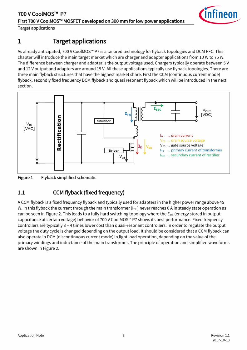
1 Target applications
As already anticipated, 700 V CoolMOS™ P7 is a tailored technology for flyback topologies and DCM PFC. This
chapter will introduce the main target market which are charger and adapter applications from 10 W to 75 W. The difference between charger and adapter is the output voltage used. Chargers typically operate between 5 V and 12 V output and adapters are around 19 V. All these applications typically use flyback topologies. There are three main flyback structures that have the highest market share. First the CCM (continuous current mode)
flyback, secondly fixed frequency DCM flyback and quasi resonant flyback which will be introduced in the next section.
Figure 1 Flyback simplified schematic
1.1 CCM flyback (fixed frequency)
A CCM flyback is a fixed frequency flyback and typically used for adapters in the higher power range above 45
W. In this flyback the current through the main transformer (ITR ) never reaches 0 A in steady state operation as can be seen in Figure 2. This leads to a fully hard switching topology where the Eoss (energy stored in output
capacitance at certain voltage) behavior of 700 V CoolMOS™ P7 shows its best performance. Fixed frequency
controllers are typically 3 – 4 times lower cost than quasi-resonant controllers. In order to regulate the output voltage the duty cycle is changed depending on the output load. It should be considered that a CCM flyback can
also operate in DCM (discontinuous current mode) in light load operation, depending on the value of the primary windings and inductance of the main transformer. The principle of operation and simplified waveforms are shown in Figure 2.

Application Note 4 Revision 1.1
2017-10-13
700 V CoolMOS™ P7 First 700 V CoolMOS™ MOSFET developed on 300 mm for low power applications
Target applications
Figure 2 CCM flyback principle of operation

Application Note 5 Revision 1.1
2017-10-13
700 V CoolMOS™ P7 First 700 V CoolMOS™ MOSFET developed on 300 mm for low power applications
Target applications
1.2 DCM flyback (fixed frequency)
As already mentioned, the DCM flyback is typically used at lower output loads. In a standard DCM flyback the
output is also regulated by the duty cycle. This setup is not used frequently due to new efficiency standards.
Also second sourcing is not always easy to achieve as the Eoss losses from a MOSFET contributes tremendously to the overall efficiency and is different for all MOSFETs available on the market. The principle of operation and simplified waveforms are shown in Figure 3 below.
Figure 3 DCM flyback principle of operation

Application Note 6 Revision 1.1
2017-10-13
700 V CoolMOS™ P7 First 700 V CoolMOS™ MOSFET developed on 300 mm for low power applications
Target applications
1.3 QR flyback (variable frequency)
Quasi-resonant (QR) flyback topologies are the most commonly used topologies for low power chargers. They
offer better performance due to lowering the switching losses. A QR flyback can only operate in DCM, because it
switches the MOSFET on during the oscillation phase of drain node capacitance and transformer main inductance when the current through the main transformer is 0 A. The difference between a standard DCM flyback and QR operation is, that the MOSFET is able to turn on at minimum VDS (drain-source voltage) which reduces the Eoss losses. This behavior is called valley switching and can be seen in the following figure.
Figure 4 QR flyback principle of operation
Typically, at very light loads, the MOSFET turns on at the later valley while at heavy loads the MOSFET turns on in the first valley. As described, the VDS oscillation is given by the capacitance value on the drain node and is influenced by the output capacitance of the MOSFET (Coss). In this case the switching frequency can be influenced by MOSFET selection.

Application Note 7 Revision 1.1
2017-10-13
700 V CoolMOS™ P7 First 700 V CoolMOS™ MOSFET developed on 300 mm for low power applications
Target applications
At the moment there are other flyback solutions, such as zero voltage switching flyback or active clamp flyback, available but these solutions are not considered in this application note. 700 V CoolMOS™ P7 is not intended to
be used in half bridge or full bridge configuration where a hard commutation of a conducting body diode can occur due to the ruggedness of the body diode.

Application Note 8 Revision 1.1
2017-10-13
700 V CoolMOS™ P7 First 700 V CoolMOS™ MOSFET developed on 300 mm for low power applications
Technology parameters
2 Technology parameters
This chapter will describe all technology related parameters that influence the behavior in the target
applications. Additionally it is worth mentioning 700 V CoolMOS™ P7 offers an ESD protection diode which gives at least class 1C in the human body model for all RDS(on) classes and offers class 2 for all products with RDS(on) of 600 mΩ or less.
2.1 Qg – gate charge
The gate charge influences the driving losses, which can tremendously influence the efficiency during light load operation or increased switching frequency.
Figure 5 Gate charge of 1400 mΩ devices at 0.6 A pulsed
As can be seen, 700 V CoolMOS™ P7 shows the lowest Qg in comparison to all former Infineon and main
competitor technologies. With this behavior P7 can be an enabler to move to higher switching frequencies
(>100 kHz) which can be beneficial to reduce the magnetic components of the design, leading to smaller form factors or higher power densities. It is clear that the driving losses are reduced by at least 40% in comparison to competitor devices.
2.2 RDS(on) – temperature dependency of on-state resistance
Also in the lower power ranges the conduction losses have an influence on the efficiency and the thermal
behavior of the overall system especially at lower input voltages such as 90 VAC or 110 VAC. In this case 700 V
CoolMOS™ P7 can offer a significant value proposition. As defined by the MOSFET structure, 700 V CoolMOS™ P7 offers the lowest RDS(on) change driven by increasing junction temperature. Figure 6 below shows this behavior.
0
1
2
3
4
5
6
7
8
9
10
0 2 4 6 8 10 12
VG
S [V
]
Qg [nC]
Gate charge of 1400 mOhm @ 0.6 A pulsed
IPS70R1K4P7S
IPS65R1K4C6
Competitor M
-40%

Application Note 9 Revision 1.1
2017-10-13
700 V CoolMOS™ P7 First 700 V CoolMOS™ MOSFET developed on 300 mm for low power applications
Technology parameters
Figure 6 RDS(on) behavior over junction temperature
At 150°C junction temperature the 700 V CoolMOS™ P7 shows around 21% lower maximum RDS(on) when
compared to Infineon's CoolMOSTM C6 family. This key parameter results in the reduction of MOSFET conduction losses in any design available.
2.3 Eoss – energy stored in output capacitance
Eoss is one of the main loss contributors during the turn on of the MOSFET. This is the energy that translates into
losses during turn on at a certain VDS voltage. In QR flyback converters, there are no Eon losses as there is no overlap between ID and VDS as the current through the main transformer is 0 A. Nevertheless, additional losses are generated at every turn on based on the amount of energy stored in the output capacitance.
0.0
0.5
1.0
1.5
2.0
2.5
3.0
3.5
4.0
-50 -25 0 25 50 75 100 125 150
RD
S(o
n),
max
[Ω
]
Tj - junction temperature [°C]
IPS70R1K4P7S
IPS65R1K4C6

Application Note 10 Revision 1.1
2017-10-13
700 V CoolMOS™ P7 First 700 V CoolMOS™ MOSFET developed on 300 mm for low power applications
Technology parameters
Figure 7 Eoss comparison of 900 mΩ devices
From the diagram it can be seen that 700 V CoolMOS™ P7 offers the lowest Eoss starting from 50 V VDS. Normally it is not possible to have a real ZVS turn-on of the MOSFET as there would be the need to increase the reflected
voltage from the secondary side to the primary side tremendously. This would also increase the bulk voltage and the drain source voltage peak during turn-off. Therefore turn-on VDS at low line is typically between 50 V
and 100 V and at high line 200 V to 300 V resulting in around 50% lower turn on losses than the main competitor M and around 25% lower than competitor S.
As these additional losses are present at every turn on, 700 V CoolMOS™ P7 also offers the possibility to achieve higher switching frequencies as already described in the gate charge section of this chapter.
2.4 Qoss – charge stored in output capacitance
It was already illustrated that valley switching is typically above 50 V drain-source voltage.
0.0
0.2
0.4
0.6
0.8
1.0
1.2
1.4
1.6
0 50 100 150 200 250 300 350 400
E oss
[u
J]
VDS [V]
IPS70R900P7S IPS60R950C6 Competitor S Competitor M

Application Note 11 Revision 1.1
2017-10-13
700 V CoolMOS™ P7 First 700 V CoolMOS™ MOSFET developed on 300 mm for low power applications
Technology parameters
Figure 8 Qoss comparison of 1400 mΩ devices
Recirculating current also leads to additional passive losses from 50 V onwards. In order to have the lowest possible recirculating current, the extremely small Qoss (1.7 nC) between 50 V and 400 present in 700 V
CoolMOS™ P7 needs the lowest circulating current to charge and discharge the Coss in comparison to competitor devices from 50 V VDS upwards.
2.5 Transfer characteristics
Around 95% of all flyback converters use peak current control. This means that the controller sends the turn off
signal to the gate driver at a certain current value present in the primary inductance of the main transformer and MOSFET. There is a well-known failure mode in charger and adapter applications when the gate source
voltage drops during burst mode operation and the MOSFET is unable to carry sufficient current to reach the peak current. In this case the MOSFET operates in the linear region and does not turn off resulting in
destruction of the MOSFET / application. In addition, 700 V CoolMOS™ P7 can offer a very narrow VGS(th) (gate source threshold voltage) window from 2.5 V to 3.5 V with a typical value of 3 V.
0
5
10
15
20
25
0 50 100 150 200 250 300 350 400
Qo
ss [
nC
]
VDS [V]
IPS70R1K4P7S
IPS65R1K4C6
Competitor M

Application Note 12 Revision 1.1
2017-10-13
700 V CoolMOS™ P7 First 700 V CoolMOS™ MOSFET developed on 300 mm for low power applications
Technology parameters
Figure 9 Transfer characteristics comparison of 1400 mΩ devices at 25°C
700 V CoolMOS™ P7 shows the best in class transconductance behavior due to unmatched current capability at
low gate-source voltage. Furthermore, this leads to the possibility to reduce the gate source voltage intentionally in order to minimize the overall driving losses and the possibility to comply with new no-load
operation requirements.
2.6 Avalanche
The general recommendation is to keep VDS below the VBR(DSS) (breakdown voltage) rating of the product shown
in datasheets. As market analysis has shown, 80% derating is used in all charger and adapter applications
during standard operation and is permitted to increase to 100% during transients. This results in an assumption that avalanche is not present in these applications. Nevertheless, there are also surge tests performed on customer applications during qualification that are only a pass/fail test where the MOSFET is not
permitted to be the root cause of a failure. In this case, it is difficult to verify if the MOSFET is driven into avalanche operation or not. It is always recommended to use a snubber network to limit the drain source
voltage overshoot. This should be dimensioned so that the snubber is active before the breakdown voltage is reached as shown in Figure 10.
0
1
2
3
4
5
6
7
8
9
10
0 2 4 6 8 10 12
I D [
A]
VGS [V]
IPS70R1K4P7S
IPS65R1K4C6
Competitor M

Application Note 13 Revision 1.1
2017-10-13
700 V CoolMOS™ P7 First 700 V CoolMOS™ MOSFET developed on 300 mm for low power applications
Technology parameters
Avalanche operation in a flyback can only be driven by the leakage inductance of the transformer, which is typically in the range of 1-2% of the main transformer primary inductance. Based on this there are much lower energies and inductance values as shown in previous MOSFET datasheets.
Figure 10 Flyback converter turn off avalanche operation
As already discussed in several publications destruction by avalanche energy with high energy and high inductance values is not typical for any SMPS application. Thus Infineon adapts the avalanche conditions in all
new datasheets for new technologies to meet the application design environment. 700 V CoolMOS™ P7 includes the current destruction mechanism rating in all datasheets. The current during the avalanche is limited by the peak current control and can therefore quite easily controlled.
In order to determine if 700 V CoolMOS™ P7 is ready for surge qualification Infineon have tested several end
customer designs and applied surge qualification directly to customer designs. The following table represents the results of this test up to design failure during surge qualification.
Table 1 Surge verification tests done in end-customer applications till design failure
Customer applications L-> N surge voltage Fail Note
10 W charger 1.5 kV fuse, bulk cap, bridge
diode
no MOSFET destruction
12 W quick charger 2 kV fuse, bulk cap, bridge
diode no MOSFET destruction
15 W charger 3 kV bridge diode no MOSFET destruction
18 W quick charger 2.5 kV fuse, bulk cap, bridge
diode no MOSFET destruction

Application Note 14 Revision 1.1
2017-10-13
700 V CoolMOS™ P7 First 700 V CoolMOS™ MOSFET developed on 300 mm for low power applications
Technology parameters
As can be seen in all surge tests, 700 V CoolMOS™ P7 survived the surge event. Generally, designers should
always use a snubber network in order to prevent avalanche operation of the MOSFET.
2.7 Early channel shutdown
In some RDS(on) classes, 700 V CoolMOS™ P7 will have an Rg,int (integrated gate resistor). In order to fit to
Infineon's “ease of use” requirement this value can be seen in all available datasheets. In end applications, external gate resistors are either used to slow down the devices for EMI reasons or for voltage peak limitation.
Nevertheless, 700 V CoolMOS™ P7 offers the so-called early channel shutdown. This means that every RDS(on)
class has a limit where the switching losses increase with respect to the gate resistance in the gate drive loop.
For 700 V CoolMOS™ P7 it is possible to increase the gate resistor without suffering switching loss increase. This is valid for all RDS(on) classes to at least 30 – 40 Ohm on the gate (the sum of internal and external gate resistors). Figure 11 below shows this as a simplified example. Furthermore, the Eoff value under same test condition of 700 V CoolMOS™ P7 is on average 35% smaller than Infineon's main competitor.
Figure 11 Early channel shutdown 700 V CoolMOS™ P7 (simplified)
Due to this behavior it is possible to properly define the end applications for safety, EMI and efficiency requirements at the same time.
Now that the key technology parameters of the 700 V CoolMOS™ P7 have been described, the next chapter will illustrate real application measurements with respect to thermal performance, efficiency and EMI.
18 W quick charger 2 2 kV fuse, bridge diode no MOSFET destruction
24 W quick charger 1.8 kV bridge diode no MOSFET destruction

Application Note 15 Revision 1.1
2017-10-13
700 V CoolMOS™ P7 First 700 V CoolMOS™ MOSFET developed on 300 mm for low power applications
Benchmarking of 700 V CoolMOS™ P7 in low power designs
3 Benchmarking of 700 V CoolMOS™ P7 in low power designs
As already anticipated, 700 V CoolMOS™ P7 is tailored for low power applications that use flyback topologies
and DCM PFCs. This chapter is intended to show the performance benefits customers can enjoy with 700 V CoolMOS™ P7 in comparison to competitors devices.
3.1 12 W customer charger
The first benchmark will show the efficiency and thermal benefits that can be achieved using 700 V CoolMOS™
P7 in a plug and play scenario while not sacrificing ease of use, especially for radiated electromagnetic interference. This 12 W customer charger is a high end single output quasi resonant flyback battery charger for mobile devices with a switching frequency of up to 140 kHz.
3.1.1 Efficiency / thermals
Typically, designers of charger or adapter applications are interested in the mold compound temperature after
30 min burn-in running at full load, the 75%, 50% and 25% load points and the average efficiency. The following diagram represents the relative efficiency comparison over the output current. The IPS70R1K4P7S is used as a reference.
Figure 12 Efficiency and thermal comparison – 12 W customer charger at 25°C ambient and 230 VAC input
voltage
@ full load

Application Note 16 Revision 1.1
2017-10-13
700 V CoolMOS™ P7 First 700 V CoolMOS™ MOSFET developed on 300 mm for low power applications
Benchmarking of 700 V CoolMOS™ P7 in low power designs
As can be seen in Figure 12, the new IPS70R1K4P7S outperforms all internal and external competitors that have an RDS(on),max of around 900 mΩ. Especially in light load operation, 700 V CoolMOS™ P7 offers 4% higher efficiency
against the competitors of this design. At full load operation and 30 minutes burn in, IPS70R1K4P7S shows the lowest mold compound temperature with ~13°C lower temperature in comparison to competitors and ~16°C lower temperature than 650 V C6.
This benchmarking shows that customers can benefit from higher efficiency and thermal performance with a 1400 mΩ device from 700 V CoolMOS™ P7 compared to 900mΩ devices from competitors. Customers may choose to use the next higher RDS(on) class to save cost. Furthermore, a better thermal performance allows designers to select cost competitive packages as SOT-223.
3.1.2 Radiated EMI
Beside efficiency and thermals, EMI is a very important factor for any charger or adapter application. Figure 13
below shows the maximum quasi-peak values of the radiated field according to EN55022B and also includes
the same competitors as included in the previous results. This measurement was performed in a European Union certified EMI chamber.
Figure 13 Radiated EMI comparison in 12 W customer charger according to EN55022B
700 V CoolMOS™ P7 exceeds the EMI specifications of EN55022B and shows more than 10 dBuV/m safety margin to the specification limits with RG,ext = 0 Ω during turn off. This customer charger, even when operating up to 140
kHz, is an excellent design with respect to EMI behavior due to the additional EMI filtering and cancellation windings. All devices have greater than 10dBuV/m margin over the specification limits showing that 700 V CoolMOS™ P7 performs at least as well as all competitors.
3.2 35 W Infineon adapter
This 35 W adapter is a single stage quasi-resonant flyback adapter that demonstrates that it is possible to run in
DCM mode for higher power applications while reducing the Eon losses to a minimum. Nevertheless, this adapter differs significantly from the 12 W customer charger as it operates between 65 kHz and 80 kHz. This measurement will show that 700 V CoolMOS™ P7 delivers best performance in higher frequency applications
but also shows the highest performance in lower frequency applications. It will prove the value of 700 V CoolMOS™ P7 in low to mid frequency ranges.
Application Note 17 Revision 1.1
2017-10-13
700 V CoolMOS™ P7 First 700 V CoolMOS™ MOSFET developed on 300 mm for low power applications
Benchmarking of 700 V CoolMOS™ P7 in low power designs
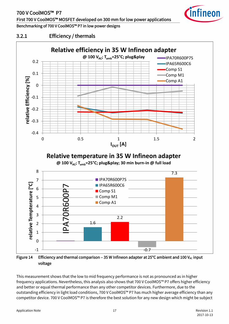
3.2.1 Efficiency / thermals
Figure 14 Efficiency and thermal comparison – 35 W Infineon adapter at 25°C ambient and 100 VAC input
voltage
This measurement shows that the low to mid frequency performance is not as pronounced as in higher
frequency applications. Nevertheless, this analysis also shows that 700 V CoolMOS™ P7 offers higher efficiency and better or equal thermal performance than any other competitor devices. Furthermore, due to the outstanding efficiency in light load conditions, 700 V CoolMOS™ P7 has much higher average efficiency than any
competitor device. 700 V CoolMOS™ P7 is therefore the best solution for any new design which might be subject
-0.4
-0.3
-0.2
-0.1
0
0.1
0.2
0 0.5 1 1.5 2
rela
tive
Eff
icie
ncy
[%
]
IOUT [A]
Relative efficiency in 35 W Infineon adapter @ 100 VAC; Tamb=25°C; plug&play IPA70R600P7S
IPA65R600C6Comp S1Comp M1Comp A1
1.6 2.2
-0.7
7.3
-1
0
1
2
3
4
5
6
7
8
rela
tive
Te
mp
tera
ture
[°C
]
Relative temperature in 35 W Infineon adapter @ 100 VAC; Tamb=25°C; plug&play; 30 min burn-in @ full load
IPA70R600P7SIPA65R600C6Comp S1Comp M1Comp A1
IPA
70
R6
00
P7

Application Note 18 Revision 1.1
2017-10-13
700 V CoolMOS™ P7 First 700 V CoolMOS™ MOSFET developed on 300 mm for low power applications
Benchmarking of 700 V CoolMOS™ P7 in low power designs
to more stringent efficiency regulations in the future. Only Competitor M1 shows a slightly lower mold compound temperature, although only within the measurement tolerance.
3.2.2 Radiated EMI
Figure 15 Radiated EMI comparison in 35 W Infineon adapter according to EN55022B
Figure 15 shows that IPA70R600P7S has a smaller maximum quasi-peak value over the whole EN55022B
frequency range than that of any other competitor. Only IPA65R600C6 shows a better radiated EMI performance but loses out with respect to efficiency due to higher gate charge and generally higher Eoff.
3.3 Benchmarking summary (key facts) for all measurements
Customers can benefit due to the ability to change to higher RDS(on) classes thus reducing overall costs.
As was illustrated earlier, 700 V CoolMOS™ P7 is an enabler for higher switching frequency applications in order to reduce the overall magnetic content of the application resulting in a smaller form factor and therefore higher power density.
700 V CoolMOS™ P7 shows its best performance at high line operation due to the Eoss behavior but shows also good performance during low line operation due to the temperature dependency of RDS(on).
700 V CoolMOS™ P7 offers an additional 50 V safety margin for 650 V applications due to the increased break down voltage.
EMI behavior depends on the application itself, but measurements have shown that it is possible to have lower radiated EMI than currently available competitor devices.
-1.48
2.53 2.64
1.55
-2.00
-1.50
-1.00
-0.50
0.00
0.50
1.00
1.50
2.00
2.50
3.00
rela
tive
EM
I rad
iate
d Q
PM
AX
[dB
µV
/m]
Relative EMI radiated QPMAX in 35 W Infineon adapter @ ~170 MHz
@ 230 VAC; Tamb=25°C; plug&play; 30 min burn-in
IPA70R600P7SIPA65R600C6Comp M1Comp S1Comp A1
IPA
70
R6
00
P7
S
Application Note 19 Revision 1.1
2017-10-13
700 V CoolMOS™ P7 First 700 V CoolMOS™ MOSFET developed on 300 mm for low power applications
Portfolio
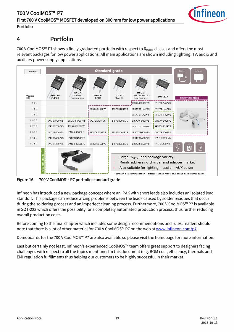
4 Portfolio
700 V CoolMOSTM P7 shows a finely graduated portfolio with respect to RDS(on) classes and offers the most
relevant packages for low power applications. All main applications are shown including lighting, TV, audio and auxiliary power supply applications.
Figure 16 700 V CoolMOSTM P7 portfolio standard grade
Infineon has introduced a new package concept where an IPAK with short leads also includes an isolated lead standoff. This package can reduce arcing problems between the leads caused by solder residues that occur
during the soldering process and an imperfect cleaning process. Furthermore, 700 V CoolMOS™ P7 is available in SOT-223 which offers the possibility for a completely automated production process, thus further reducing overall production costs.
Before coming to the final chapter which includes some design recommendations and rules, readers should note that there is a lot of other material for 700 V CoolMOS™ P7 on the web at www.infineon.com/p7.
Demoboards for the 700 V CoolMOS™ P7 are also available so please visit the homepage for more information.
Last but certainly not least, Infineon's experienced CoolMOSTM team offers great support to designers facing challenges with respect to all the topics mentioned in this document (e.g. BOM cost, efficiency, thermals and EMI regulation fulfillment) thus helping our customers to be highly successful in their market.

Application Note 20 Revision 1.1
2017-10-13
700 V CoolMOS™ P7 First 700 V CoolMOS™ MOSFET developed on 300 mm for low power applications
Design considerations
5 Design considerations
The last chapter will describe the most relevant design considerations.
5.1 Paralleling of MOSFETs
Typically, these applications do not use paralleled MOSFETs, nevertheless in order to parallel MOSFETs a gate ferrite bead is always recommended. Appropriate values depend on the parasitics of the PCB itself.
5.2 Source impedance (source bead)
Source impedances are used in order to slow down the di/dt on the drain path resulting in a lower drain source
overvoltage peak. Nevertheless, it also induces a voltage drop during turn on and turn off that can lead to
oscillations in the gate drive loop. This influences the general EMI behavior and could also lead to destruction of any MOSFET if this voltage oscillation drives the gate source voltage over +30 V or under -30 V.
Therefore a source bead is not recommended to limit a possible overvoltage peak from drain to source.
5.3 Target applications
700 V CoolMOSTM P7 is not permitted to be used in half or full bridge configurations or any other topology where a hard commutation on a conducting body diode can appear.

Application Note 21 Revision 1.1
2017-10-13
Revision history
700 V CoolMOS™ P7 First 700 V CoolMOS™ MOSFET developed on 300 mm for low power applications
Revision history
Major changes since the last revision
Page or Reference Description of change
P19 Updated product portfolio

Trademarks of Infineon Technologies AG AURIX™, C166™, CanPAK™, CIPOS™, CoolGaN™, CoolMOS™, CoolSET™, CoolSiC™, CORECONTROL™, CROSSAVE™, DAVE™, DI-POL™, DrBlade™, EasyPIM™, EconoBRIDGE™, EconoDUAL™, EconoPACK™, EconoPIM™, EiceDRIVER™, eupec™, FCOS™, HITFET™, HybridPACK™, Infineon™, ISOFACE™, IsoPACK™, i-Wafer™, MIPAQ™, ModSTACK™, my-d™, NovalithIC™, OmniTune™, OPTIGA™, OptiMOS™, ORIGA™, POWERCODE™, PRIMARION™, PrimePACK™, PrimeSTACK™, PROFET™, PRO-SIL™, RASIC™, REAL3™, ReverSave™, SatRIC™, SIEGET™, SIPMOS™, SmartLEWIS™, SOLID FLASH™, SPOC™, TEMPFET™, thinQ!™, TRENCHSTOP™, TriCore™. Trademarks updated August 2015
Other Trademarks All referenced product or service names and trademarks are the property of their respective owners. AN_201701_PL52_006owners.
Edition 2017-10-13
AN_201701_PL52_006
Published by
Infineon Technologies AG
81726 Munich, Germany
© 2017 Infineon Technologies AG.
All Rights Reserved.
Do you have a question about this document?
Email: [email protected]
Document reference
IMPORTANT NOTICE The information contained in this application note is given as a hint for the implementation of the product only and shall in no event be regarded as a description or warranty of a certain functionality, condition or quality of the product. Before implementation of the product, the recipient of this application note must verify any function and other technical information given herein in the real application. Infineon Technologies hereby disclaims any and all warranties and liabilities of any kind (including without limitation warranties of non-infringement of intellectual property rights of any third party) with respect to any and all information given in this application note. The data contained in this document is exclusively intended for technically trained staff. It is the responsibility of customer’s technical departments to evaluate the suitability of the product for the intended application and the completeness of the product information given in this document with respect to such application.
For further information on the product, technology, delivery terms and conditions and prices please contact your nearest Infineon Technologies office (www.infineon.com).
WARNINGS Due to technical requirements products may contain dangerous substances. For information on the types in question please contact your nearest Infineon Technologies office. Except as otherwise explicitly approved by Infineon Technologies in a written document signed by authorized representatives of Infineon Technologies, Infineon Technologies’ products may not be used in any applications where a failure of the product or any consequences of the use thereof can reasonably be expected to result in personal injury.