75ds2 3u cpci synchro/resolver or lvdt/rvdt...
TRANSCRIPT

75DS2 Operations Manual North Atlantic Industries, Inc. 11/11/2011 Rev: 2011-11-11-1000 www.naii.com Page 1 of 43
75DS2 3U cPCI SYNCHRO/RESOLVER or
LVDT/RVDT CONVERTER
OPERATIONS MANUAL

75DS2 Operations Manual North Atlantic Industries, Inc. 11/11/2011 Rev: 2011-11-11-1000 www.naii.com Page 2 of 43
MODEL 75DS2
3U cPCI SYNCHRO/RESOLVER or LVDT/RVDT CONVERTER
Convection Cooled
Features
1, 2, 3, or 4 Synchro/Resolver (D/S) or LVDT/RVDT (DLV) simulation channels
1 arc-minute (0.0167°) accuracy
16 bit resolution
1.5, 2.2 or 3 VA drive capability per synchro channel
Automatic background BIT testing continually checks and reports the health of each channel
Optional onboard 3 VA programmable reference supply
Connections via front panel, rear connector or both
Convection and conduction-cooled
Wrap-around converters for reading actual commanded outputs
No adjustments or trimming required
Wide operating temperature range Software support kit and drivers are
available
Conduction Cooled
Description
The 75DS2 is a 3U cPCI board which incorporates up to 4 Digital-to-Synchro/Resolver converters with 1.5, 2.2 or 3 VA drive capability; or 2 or 4 isolated DLV converters. The board features continuous background BIT testing, reference and signal loss detection. Each channel is independent, isolated and enables the user to ground one of the outputs without affecting performance. This model drives passive or active loads. In addition, the card provides an optional onboard reference supply.
Automatic background BIT testing, an important feature, is always enabled and continually checks the health of each channel. There is no need to guess or make assumptions about system performance. A fault is immediately reported and the specific channel is identified. This diagnostic capability is of tremendous benefit because it immediately identifies and reports a failure, without the need to shut down the equipment for troubleshooting. Testing is totally transparent to the user, requires no external programming, and has no effect on the standard operation of the card.

75DS2 Operations Manual North Atlantic Industries, Inc. 11/11/2011 Rev: 2011-11-11-1000 www.naii.com Page 3 of 43
Table of Contents MODEL 75DS2 ...........................................................................................................................................................2
3U CPCI SYNCHRO/RESOLVER OR LVDT/RVDT CONVERTER ..........................................................................2
FEATURES ................................................................................................................................................................2
DESCRIPTION ...........................................................................................................................................................2
SPECIFICATIONS ......................................................................................................................................................6
General – for the Mother Board ............................................................................................................................................... 6 D/S (Module 3*, 4*) – One Isolated Digital-to-SYN/RSL Ch, 3.0 VA Output ............................................................................ 6 D/S (Module 1*,2*) – Two Isolated Digital-to-SYN/RSL Ch, 1.5/2.2 VA Outputs ..................................................................... 6 DLV (Module 5*) – Two/Four Isolated DLV Simulation Ch, LVDT/RVDT Outputs ................................................................... 7 Reference (Module W6, W7)– Optional, Isolated, On-Board Reference Supply ..................................................................... 8 Product Configuration and Memory Map ................................................................................................................................. 9 MEMORY MAP........................................................................................................................................................................ 9
D/S ONE/TWO CHANNEL (MODULES 1*, 2*, 3*, 4*) ............................................................................................ 10
Principle of Operation ............................................................................................................................................................ 10 Built-In Test (BIT) / Diagnostic Capability .............................................................................................................................. 10 Wrap S/D Angle (Read) ......................................................................................................................................................... 11 Measured Reference Voltage ................................................................................................................................................ 11 Measured Signal Voltage ...................................................................................................................................................... 11 Signal Loss Threshold ........................................................................................................................................................... 11 Reference Loss Threshold .................................................................................................................................................... 11 D/S Channel Frequency ........................................................................................................................................................ 11 D/S Status, Signal Loss ......................................................................................................................................................... 12 D/S Wrap Select, Internal/External (Pending) ....................................................................................................................... 12 D/S Status, External Amplifier (Pending) ............................................................................................................................... 12 D/S Write Angle – Single Speed ............................................................................................................................................ 12 D/S Write Angle – Two Speed ............................................................................................................................................... 12 D/S Rotation .......................................................................................................................................................................... 13 D/S Stop Angle ...................................................................................................................................................................... 13 D/S Set Rotation Rate ........................................................................................................................................................... 13 D/S Rotation Mode, Continuous or Start/Stop ....................................................................................................................... 13 D/S Rotation Status ............................................................................................................................................................... 13 Start Rotation ........................................................................................................................................................................ 13 Stop Rotation ......................................................................................................................................................................... 13 D/S Set Reference Voltage ................................................................................................................................................... 14 D/S Set Signal Voltage .......................................................................................................................................................... 14 D/S BIT Test Enable .............................................................................................................................................................. 14 D/S Status, BIT Test .............................................................................................................................................................. 15 Test (D2) Verify ..................................................................................................................................................................... 15 D/S Ratio 1/2 ......................................................................................................................................................................... 15 D/S Output Mode ................................................................................................................................................................... 15 D/S Synchro / Resolver Select .............................................................................................................................................. 16 D/S Torque Receiver Select .................................................................................................................................................. 16 D/S Trigger Source Select ..................................................................................................................................................... 16 D/S Trigger Slope Select ....................................................................................................................................................... 16 D/S Module Power Enable .................................................................................................................................................... 16 D/S Output Enable ................................................................................................................................................................. 16 D/S Active Channel Select .................................................................................................................................................... 17 D/S Status, Reference Loss .................................................................................................................................................. 17 D/S Status, Phase Lock Loss ................................................................................................................................................ 17 D/S Set Phase Offset ............................................................................................................................................................ 17 Reference Loss Interrupt Enable ........................................................................................................................................... 17 Signal Loss Interrupt Enable ................................................................................................................................................. 18 BIT Test Fail Interrupt Enable ................................................................................................................................................ 18 Phase Lock Loss Interrupt Enable ......................................................................................................................................... 18 OSC (Optional Onboard Reference Supply) Set Frequency ................................................................................................. 18 OSC (Optional Onboard Reference Supply) Set Voltage ...................................................................................................... 19 Interrupt Vector ...................................................................................................................................................................... 19
D/S (1*, 2*, 3*, 4*) (PCI) MODULE MEMORY MAP ............................................................................................... 20
DLV TWO/FOUR CHANNEL (MODULE 5*) ........................................................................................................... 21
Principle of Operation ............................................................................................................................................................ 21

75DS2 Operations Manual North Atlantic Industries, Inc. 11/11/2011 Rev: 2011-11-11-1000 www.naii.com Page 4 of 43
Built-in Test/Diagnostic Capability ......................................................................................................................................... 21 Wrap LVDT Position (Read) .................................................................................................................................................. 21 Wrap (LVDT) Velocity ............................................................................................................................................................ 22 DLV Channel Signal Voltage ................................................................................................................................................. 22 DLV Channel Excitation Voltage............................................................................................................................................ 22 Signal Loss Threshold ........................................................................................................................................................... 22 Excitation Loss Threshold ..................................................................................................................................................... 22 DLV Write Position ................................................................................................................................................................ 22 DLV Response / Filter Time .................................................................................................................................................. 22 Status, Signal Loss ................................................................................................................................................................ 23 DLV Channel Frequency ....................................................................................................................................................... 23 DLV Set Channel Excitation Voltage ..................................................................................................................................... 23 DLV Set Channel Signal Voltage ........................................................................................................................................... 23 DLV BIT Test Enable ............................................................................................................................................................. 24 Test (D2) Verify ..................................................................................................................................................................... 24 DLV Output Mode .................................................................................................................................................................. 24 DLV 2-Wire or 3/4-Wire Select .............................................................................................................................................. 24 DLV Module Power Enable ................................................................................................................................................... 25 DLV Current .......................................................................................................................................................................... 25 DLV Active Channel Select ................................................................................................................................................... 25 DLV Status, Excitation Loss .................................................................................................................................................. 25 DLV Status, Phase Lock Loss ............................................................................................................................................... 25 DLV Set Phase Offset ........................................................................................................................................................... 25 DLV Current Threshold .......................................................................................................................................................... 25 OSC (Onboard) Excitation Set Frequency ............................................................................................................................. 26 OSC (Onboard) Excitation Set Voltage ................................................................................................................................. 26 DLV Status, BIT Test ............................................................................................................................................................. 27 Excitation Loss Interrupt Enable ............................................................................................................................................ 27 Signal Loss Interrupt Enable ................................................................................................................................................. 27 BIT Test Fail Interrupt Enable ................................................................................................................................................ 27 Phase Lock Loss Interrupt Enable ......................................................................................................................................... 27 Interrupt Vector ...................................................................................................................................................................... 28
2/4 CH DLV (5*) (PCI) MODULE MEMORY MAP .................................................................................................. 29
OPTIONAL ONBOARD REFERENCE CONTROL ................................................................................................ 30
OSC (Optional Onboard Reference Supply) Set Frequency ................................................................................................. 30 OSC (Optional Onboard Reference Supply) Set Voltage ...................................................................................................... 30 PCI Memory Map ................................................................................................................................................................... 30
GENERAL USE REGISTER MEMORY MAP ......................................................................................................... 31
MEMORY MAP...................................................................................................................................................................... 31 Part Number .......................................................................................................................................................................... 31 Serial Number........................................................................................................................................................................ 31 Date Code ............................................................................................................................................................................. 31 Revisions ............................................................................................................................................................................... 31 Board Ready ......................................................................................................................................................................... 31 Watchdog Timer .................................................................................................................................................................... 31 Soft Reset .............................................................................................................................................................................. 31 Design Version ...................................................................................................................................................................... 31 Platform ................................................................................................................................................................................. 32 Model ..................................................................................................................................................................................... 32 Generation ............................................................................................................................................................................. 32 Special Spec ......................................................................................................................................................................... 32 Interrupt Flow for PCI/cPCI .................................................................................................................................................... 33
75DS2 CONNECTOR/PIN-OUT INFORMATION ................................................................................................... 34
Front Panel Connectors J3, J4: ............................................................................................................................................. 34 Rear Panel Connectors J1, J2: .............................................................................................................................................. 34 Optional Onboard Reference Output ..................................................................................................................................... 34 NAI Synchro / Resolver Naming Convention ......................................................................................................................... 35 SLOT 1 D/S OR DLV ............................................................................................................................................................. 35 SLOT 2 D/S OR DLV ............................................................................................................................................................. 36 Dimensions ............................................................................................................................................................................ 37
PART NUMBER DESIGNATION ............................................................................................................................ 38
Two Channel D/S Module Code Table .................................................................................................................................. 40

75DS2 Operations Manual North Atlantic Industries, Inc. 11/11/2011 Rev: 2011-11-11-1000 www.naii.com Page 5 of 43
Single Channel D/S Module Code Table ............................................................................................................................... 41 2/4 Channel DLV Module Code Table ................................................................................................................................... 42
REVISION PAGE .................................................................................................................................................... 43

Specifications
75DS2 Operations Manual North Atlantic Industries, Inc. 11/11/2011 Rev: 2011-11-11-1000 www.naii.com Page 6 of 43
SPECIFICATIONS
General – for the Mother Board Signal Logic Level: Automatically supports either 5V or 3.3V CPCI bus Power (Motherboard): +5 VDC @ 750mA and ±12V @ 15mA, then add pwer for each individual
module Temperature, Operating: “C” =0°C to +70°C; “E” =-40°C to +85°C (See part number) Storage Temperature: -55°C to +105°C Size: Height -3.94” / 100 mm (3U)
Width -0.8” / 20.3 mm (4HP) Depth – 6.3” / 160 mm
Weight: 4 oz. (115 g) unpopulated, Add weight for each module (typically 1 oz. each) Add 2oz. (57g) for reference supply Add 2 oz. (57g) for wedgelocks
D/S (Module 3*, 4*) – One Isolated Digital-to-SYN/RSL Ch, 3.0 VA Output *See P/N (Applies to each channel unless noted otherwise)
Resolution: 16 bits (.0055°) Accuracy: 0.067º (4 arc minutes) for passive loads; 30 arc minutes for TR’s Output Format: Synchro or Resolver, (see part number), galvanic isolation Output Voltage: (See code table and part number) Output Load: 3.0 VA max. /Channel. Short circuit protected Output Control: Channel output can be turned ON/OFF Regulation (VL-L): 5% max. No load to Full load Rotation: Continuous rotation or programmable Start and Stop angles. 0 to 13.6 RPS with a
resolution of 0.15/sec. Step size is 16 bits (0.0055)° up to 1.5 RPS, then linearly increases to 12 bits (0.088°) at 13.6 RPS
Reference Input Voltage: 2 to 115Vrms, Galvanic isolated. Uses @ 1 ma max/Channel Reference Frequency: 47 Hz to 10 KHz (See part number) Phase Shift: 0.5° max. (Between output and reference) Programmable Phase Shift: Programmable, ± 90 with 0.1 resolution Settling Time: Less than 100 microseconds Module Power: +5VDC @ 50 mA
±12VDC @ 115 mA (no-load); (Add 1.1 watts of ±12V for every VA of output). Therefore, a 3.0 VA Load adds to ±12VDC 138 mA average, or 157 mA peak External ±12VDC input power can be utilized
Ground: Isolated signal and reference. Channels individually isolated from each other and from system ground
Weight: 1.5 oz. (42g)
D/S (Module 1*,2*) – Two Isolated Digital-to-SYN/RSL Ch, 1.5/2.2 VA Outputs *See P/N (Applies to each channel unless noted otherwise)
Resolution: 16 bits (.0055°)
Accuracy: ±1 arc-minute (.017°) from No Load to Full Load
Output Format: Synchro or Resolver (see part number), galvanic isolation
Output Voltage: (See code table and part number) Output Load: 1.5 VA @ 11.8 VLL or 28 VLL, and 2.2 VA @ 90 VLL max. per Channel
(Power reduces linearly as output voltage is reduced.) Shortcut circuit protected Output Control: Module outputs can be turned ON/OFF
Regulation (VL-L): 5% max. No load to Full load

Specifications
75DS2 Operations Manual North Atlantic Industries, Inc. 11/11/2011 Rev: 2011-11-11-1000 www.naii.com Page 7 of 43
Ratio: Dual speed, Programmable, Set any ratio between 2 and 255
Rotation: Continuous rotation or programmable Start and Stop angles. 0 to 13.6 RPS with
a resolution of 0.015/sec. Step size is 16 bits (0.0055)° up to 1.5 RPS, then linearly increases to 12 bits (0.088°) at 13.6 RPS Reference Input Voltage: 2 to 115Vrms, Galvanic isolation. Uses 1 ma max/Channel
Reference Frequency: 47 Hz to 10 KHz (See part number)
Phase Shift: 0.5° max. (between output and reference)
Programmable Phase Shift: Programmable, ± 90 with 0.1 resolution Settling Time: Less than 100 microseconds
Module Power: +5VDC @ 570 mA ±12VDC @ 160 mA (no-load) per channel (Add 2.9 watts of ±12VDC for every VA of output per channel) Therefore, a 1.5 VA Load adds to ±12V 181 mA average, or 288 mA peak per channel External ±12V input power can be utilized
Ground: Isolated signal and reference. Channels individually isolated from each other and from system ground
Weight: 1.5 oz. (42 g)
DLV (Module 5*) – Two/Four Isolated DLV Simulation Ch, LVDT/RVDT Outputs *See P/N (Applies to each channel unless noted otherwise) Number of Channels: 2 (3/4-wire) / 4 (2-wire) Resolution: 16 bits (.001526% FS) Linearity: 0.1% FS Output Gain: 0.1% Output Format: Configurable for either 3/4-wire or 2-wire.Galvanically isolated. Output voltage
is programmable fixed or ratio-metric Output Voltage: Programmable (See code table and part number) Output Load: 1.5 VA max @ 11.8 VRMS or 28 VRMS (de-rates linearly as voltage is
decreased) (See code table) Regulation (VL-L): 5% max. No load to Full load Excitation Input Voltage: (See part number), Galvanic isolated. Uses 1 ma max/Channel Excitation Frequency: 47 Hz to 10 kHz (See part number) Phase Shift (A/B): 0.5° max. (Between output and reference) (Programmable phase shift) Settling Time: Less than 100 microseconds Module Power: +5VDC @ 570 mA ±12VDC @ 160 mA (no-load) per channel. (Add 2.9 watts of ±12VDC for every
VA of output per channel). Therefore, a 1.5 VA Load adds to ±12V 181 mA average, or 288 mA peak per channel
External ±12V input power can be utilized Ground: Isolated signal and excitation; Channels individually isolated from each other
and from system ground Weight: 1.5 oz. (42g)

Specifications
75DS2 Operations Manual North Atlantic Industries, Inc. 11/11/2011 Rev: 2011-11-11-1000 www.naii.com Page 8 of 43
Voltage (V) Output (Programmed)
Po
wer
Outp
ut
(VA
)
2.0
4.0
6.0
30
25
20
15
10
Max Current ~ 420 mA
Power Derating Curves:
Voltage Range (Vrms) Max Current (mA) Power Derating
2 - 11.9 420 5 VA @ 11.8 Vrms
(Power derates linearly to 0.84 VA @ 2.0 Vrms)
12 - 27.9 420 to 192 5 VA @ 26.0 Vrms (Power constant to 12.0 Vrms)
115 43 5 VA @ 115 Vrms (fixed)
5
2 - 10 V Frequency Range: 47 – 15000 Hz
(5 VA max @ 15 KHz then reduces linearly to 1.5 VA @ 20 KHz
10.1 – 28 V Frequency Range: 47 – 10000 Hz
5VA Power Constant
Max Current ~ 420mA to 192 mA
(w/ voltage inversely proportional)
0.5
1.4
Reference (Module W6, W7)– Optional, Isolated, On-Board Reference Supply Voltage Output:
Note: Identify voltage output option in P/N option selection
(Improved version to 5 VA introduced DOM 6/11) Vrms to 28 Vrms, Programmable with a resolution of 0.1 V
2.0 to 10.0 Vrms / 47 Hz to 20 KHz frequency range 10.1 to 28.0 Vrms / 47 Hz to 10 KHz frequency range
or
115 Vrms fixed
115.0 Vrms / 47 Hz to 2.0 KHz frequency range Accuracy (No Load): 2% of setting ≤ 10 KHz 5% of setting > 10 KHz Regulation: 10% (No Load to Full Load) Output Drive: 5 VA maximum ≤ 15 KHz
5 VA – 1.5 VA (decreased linearly from 15 KHz to 20 KHz) (See detailed description of Output Drive)
Output Protection: Over-current (10x automatic retry; @ 1.3 sec int.; afterwards, shutdown w/ manual reset)
Frequency: 47 Hz to 20 KHz Programmable with 0.1 Hz steps Frequency Accuracy: 0.1% of programmed frequency or 1 Hz (whichever is greater) THD: 2% (maximum) Reference Output Drive: (See detailed characterization) Power: +5 VDC @ 10 mA ±12 VDC @ 120 mA (Quiescent, no load, max) Add ±12 VDC @ 40 mA for every 1 VA Load Ground: Output isolated from system ground Weight: 1 oz. (28g)

Specifications
75DS2 Operations Manual North Atlantic Industries, Inc. 11/11/2011 Rev: 2011-11-11-1000 www.naii.com Page 9 of 43
Product Configuration and Memory Map This design provides multiple functions on a single cPCI (3U) card. When ordering, the customer selects an assortment of up to 2 modules to populate this 2-slot “motherboard.” The memory map follows the order of modules specified in the part number.
To address the register of any module, use the Base address to the entire card, add the Module Offset depending upon its slot (000 or 800), and then add the Register Offset of interest (see module memory map.) The memory map of each selected module counts from, or is superimposed over its respective module offset. Thus, Address = Base + Module Offset + Register Offset.
For example, if a Digital I/O module were selected to populate module 1 and a Discrete I/O module were selected to populate module 2:
Address = Base + Module 1 Offset 000 + Digital I/O register 010 = Base + 010 hex
Address = Base + Module 2 Offset 800 + Discrete I/O register 024 = Base + 824 hex
MEMORY MAP 000 Module 1 Register… 800 Module 2 Register… 3000 Unit Level General Register…
004 804 3004
008 808 3008
00C 80C 300C
010 810 3010
. . .
. . .
. . .
7FE FFE 37FE
7FF FFF 37FF
Any address NOT SPECIFIED within 4096 byte block (up to 3FFFh) is reserved. The memory map of each module type is described hereafter:
Slot 2 Offset 800
Slot 1 Offset 000
General Offset 3000

D/S One/Two Channel (Modules 1*, 2*, 3*, 4*)
75DS2 Operations Manual North Atlantic Industries, Inc. 11/11/2011 Rev: 2011-11-11-1000 www.naii.com Page 10 of 43
2
Wrap-Around
Test
S/D
DS 1
DS 2
State
Machine
DS Module Block Diagram
Mo
du
le B
us
Use
r In
terf
ace
Wrap-Around
Test
S/D
Signal and Reference
Isolation
1
D/S ONE/TWO CHANNEL (MODULES 1*, 2*, 3*, 4*) (*See part number designation)
Principle of Operation These new Digital-to-Synchro/Resolver (D/S) modules are solid state designs that eliminate the need for external transformers. Since these modules operate down to 50 Hz, deleting the previously large external transformers offers huge space savings. The reduced size and lower power consumption of these modules now makes it possible to supply 10 channels on a 6U card. Two different modules are available within the same package size: The first is a two-channel 1.5VA/2.2VA design that contains two separate channels within one enclosure. The other is a single channel 3.0VA design that will also drive Torque Receivers. All outputs are short circuit protected and the S2 (Z) leg can be grounded without effecting performance. Any channel can be programmed for rotation (either continuous or with start/stop angles). External amplifiers can be added to drive up to 30 VA with a frequency range of 50 to 400 Hz. Two-speed (up to 1:255 ratio) outputs can be programmed (dual channel module). The processor will set a flag when it
senses that the maximum allowable misalignment of 90/gear ratio is exceeded. New features in these modules now include a wrap capability for measuring each channel’s commanded output angle and carrier frequency. The module’s extensive programmability now includes format selection (synchro or resolver). A background calibration feature (pending), that is totally transparent to the operation of the channels, constantly adjusts outputs for all load and environmental conditions. Each channel can be programmed for a different output voltage, which can be programmed for either ratio-metric or absolute (fixed) output. Module power ON/OFF capability provided for shutting down inactive channels.
Built-In Test (BIT) / Diagnostic Capability Two different tests (one on-line and one off-line) can be selected: The on-line (D2) Test initiates automatic background BIT testing that checks the output accuracy of each channel by comparing the measured output angle to the commanded angle. Each channel is individually checked
to an accuracy of 0.2 and each D/S Signal output and Reference input is continually monitored. User can periodically clear to 00h and then read Test (D2) verification register again, after 0.1 seconds, to verify that background bit testing is activated. Any failure triggers an Interrupt (if enabled) and the results are available in Status Registers. The testing is totally transparent to the user, requires no external programming, has no effect on the standard operation of the card, and can be enabled or disabled.
The off-line (D3) Test initiates a BIT test that generates and tests 24 different angles to a test accuracy of 0.2. Results can be read from registers. External reference is required and outputs must be on. Any failure triggers an Interrupt (if enabled). Testing requires no external programming, and can be initiated or stopped at any time.
CAUTION: Outputs must be ON and Reference supplied during this test and therefore active. Check connected loads for possible interaction.

D/S One/Two Channel (Modules 1*, 2*, 3*, 4*)
75DS2 Operations Manual North Atlantic Industries, Inc. 11/11/2011 Rev: 2011-11-11-1000 www.naii.com Page 11 of 43
Wrap S/D Angle (Read) The Wrap S/D Angle reads back the actual output signal (angle), which is used to verify that the actual output is set to commanded angle. Read individual channels 1 or 2.
D15 D14 D13 D12 D11 D10 D9 D8 D7 D6 D5 D4 D3 D2 D1 D0
Wrap S/D Data () Hi 180 90 45 22.5 11.25 5.625 2.813 1.406 .703 .352 .176 .088 .044 .022 .011 .0055
Wrap S/D Data () Lo .00274 .00137 .00068 .00034 .00017 .00008 .00004 .00002 X X X X X X X X
Measured Reference Voltage Each individual channel input signal voltage “VREF” is measured and the value reported to a corresponding read register. The input voltage is reported to a resolution of 10 mv rms. The output is in integer decimal format. For example, if channel 1 input REF voltage is 26.0 VRMS, the output measurement word from the corresponding register would be 2600.
Measured Signal Voltage Each individual channel input signal voltage “VL-L” is measured and the value reported to a corresponding read register. The input voltage is reported to a resolution of 10 mv rms. The output is in integer decimal format. For example, if channel 1 input signal voltage is 11.8 VRMS, the output measurement word from the corresponding register would be 1180.
Signal Loss Threshold Each individual channel input signal voltage “VL-L” is measured and the value reported to a corresponding read register. The signal loss detection circuitry can be tailored to report a signal loss (at Signal Loss Status register) at a user defined threshold. This threshold can be set to a resolution of 10 mv rms. Program the threshold by writing the value of the voltage threshold in integer decimal format. For example, if channel 1 input signal loss voltage threshold is to be 7 VRMS, the programmed word to the corresponding register would be 700 (2BCh).
Reference Loss Threshold Each individual channel input reference voltage “VREF” is measured and the value reported to a corresponding read register. The reference loss detection circuitry can be tailored to report a reference loss (at Reference Loss Status register) at a user defined threshold. This threshold can be set to a resolution of 10 mv rms. Program the threshold by writing the value of the voltage threshold in integer decimal format. For example, if channel 1 input reference loss voltage threshold is to be 20 VRMS, the programmed word to the corresponding register would be 2000 (7D0h).
D/S Channel Frequency Each individual channel Reference Frequency is measured and the value reported to a corresponding read register. The input reference frequency is reported to a resolution of 1 Hz. The output is in integer decimal format. For example, if channel 1 input excitation is 400 Hz, the output measurement word from the corresponding register would be 400.

D/S One/Two Channel (Modules 1*, 2*, 3*, 4*)
75DS2 Operations Manual North Atlantic Industries, Inc. 11/11/2011 Rev: 2011-11-11-1000 www.naii.com Page 12 of 43
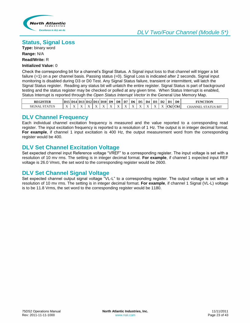
D/S Status, Signal Loss Type: binary word
Range: N/A
Read/Write: R
Initialized Value: 0
Check the corresponding bit for a channel’s Signal Loss Status. A Signal input loss to that channel will trigger a bit failure (=1) on a per channel basis; Passing status (=0). Signal Loss is indicated after 2 seconds. Signal input monitoring is disabled during D3 or D0 Test. Any Signal Status failure, transient or intermittent, will latch the Signal Status register. Reading any status bit will unlatch the entire register. Signal Status is part of background testing and the status register may be checked or polled at any given time. When Status Interrupt is enabled, Status Interrupt is reported through the Open Status Interrupt Vector in the General Use Memory Map.
REGISTER D15 D14 D13 D12 D11 D10 D9 D8 D7 D6 D5 D4 D3 D2 D1 D0 FUNCTION
D/S Status, Signal Loss X X X X X X X X X X X X X X Ch2 Ch1 CHANNEL STATUS BIT
D/S Wrap Select, Internal/External (Pending) This register sets and determines where the wrap signal will be read from and will update in the Wrap S/D Angle register. When set for internal, the wrap will be reading from the module output. When set for external, the wrap will be reading from the external amplifier wrap input signals (See pin-out). “0” = internal wrap select, “1” = external amplifier wrap select.
D15 D14 D13 D12 D11 D10 D9 D8 D7 D6 D5 D4 D3 D2 D1 D0
Wrap Select, Internal/External X X
X
X
X
X
X X
X
X
X
X
X
X
CH2 CH1
D/S Status, External Amplifier (Pending) This monitors the external amplifier BIT signal (See pin-out). Check the corresponding BIT status of the register for each active channel that has the external amplifier enabled/connected. A “1” = BIT (OK), “0” = BIT (Fail)
D15 D14 D13 D12 D11 D10 D9 D8 D7 D6 D5 D4 D3 D2 D1 D0
Status, External Amplifier X X
X
X
X
X
X X
X
X
X
X
X
X
CH2 CH1
D/S Write Angle – Single Speed Write the desired commanded output angle. For single-speed applications (Ratio=1), write an “up to” 24-bit
integer (24-bit 2’s compliment integer) to the corresponding channel D/S Write Angle register. (ex. 330 (in 16-bit
resolution) = EAABh written to Data Hi register only); 330 (in 24-bit resolution) = EAAAAB – note that “EAAA” is written to Data Hi register and “AB00” is written to Data Lo register).
WORD = (Angle (360/224
)).
D15 D14 D13 D12 D11 D10 D9 D8 D7 D6 D5 D4 D3 D2 D1 D0
D/S Write Data () Hi 180 90 45 22.5 11.25 5.625 2.813 1.406 .703 .352 .176 .088 .044 .022 .011 .0055
D/S Write Data () Lo .00274 .00137 .00068 .00034 .00017 .00008 .00004 .00002 X X X X X X X X
Note: Writing to an Input Angle Register will stop any rotation initiated on that channel
D/S Write Angle – Two Speed The dual channel module can automatically simulate two-speed applications (applies only to dual channel modules). Write an “up to” 24-bit integer (24-bit 2’s compliment integer) to the corresponding channel D/S Write Angle register to the coarse channel (channel 1). By entering a ratio in the D/S Ratio 1/2 register, the fine channel (channel 2) will automatically output a signal proportional to the programmed coarse channel times the ratio programmed.

D/S One/Two Channel (Modules 1*, 2*, 3*, 4*)
75DS2 Operations Manual North Atlantic Industries, Inc. 11/11/2011 Rev: 2011-11-11-1000 www.naii.com Page 13 of 43
D/S Rotation Each channel may be configured for either start/stop or continuous rotation for applications that require it. In start/stop mode, the user can program a rotational velocity and a stop angle. When triggered, either via a software command or external pulse (selectable trigger mode), the output signal will start at the current position and simulate rotation at the specified rotation rate and stop at the programmed stop angle. Re-initiating the trigger will repeat the rotation. In continuous mode, the user will program a rotation rate and trigger the start of the rotation either via software command or external trigger. Stopping rotation can be accomplished by either issuing a stop rotation command or setting a commanded angle. Clockwise or counter-clockwise rotation is accomplished by setting either a positive or negative 2’s complement word in the velocity register. Note: Writing to an Input Angle Register will stop any rotation initiated on that channel.
D/S Stop Angle May be used during implementation of D/S rotation. When the channel is set for start/stop rotation (D/S Rotation Mode register), write the desired stop angle to this register. Write a 16-bit integer (or 16-bit 2’s compliment
integer) to the corresponding channel D/S Write Angle register. (ex. 330 = EAABh).
WORD = (Angle (360/216
)).
D/S Set Rotation Rate May be used during implementation of D/S rotation. Write to the corresponding Set Rotation Rate registers (Hi
and Lo) a 2’s complement number representing the desired rotation rate, LSB = 0.015/sec.
Ex: 12 RPS = (12 x 360/0.015 = 288000 = 46500h), -12 RPS = (-12 x 360/0.015 = -288000 = 0xB9B00h)
Step size is 16 bits (0.0055) for up to 1.5 RPS, and then linearly decreases to 12 bits (0.088) at 13.6 RPS.
D/S Rotation Mode, Continuous or Start/Stop For continuous rotation, set the corresponding channel bit to "0" in the Rotation Mode register. For rotation to cease at a designated stop angle, set the bit to "1". For 2-speed applications, only the odd (coarse) channel needs to be programmed (CH1).
D15 D14 D13 D12 D11 D10 D9 D8 D7 D6 D5 D4 D3 D2 D1 D0
D/S Rotation Mode X X
X
X
X
X
X X
X
X
X
X
X
X
CH2 CH1
D/S Rotation Status Check the corresponding bit of the D/S Rotation Status Register for condition of rotation (“Done” or “Not Done”) for each channel. A ”1” means Rotation Done (output is static), “0” means Rotation Not Done (output is rotating) on channel. Rotation monitoring is always enabled.
D15 D14 D13 D12 D11 D10 D9 D8 D7 D6 D5 D4 D3 D2 D1 D0
D/S Status, Rotation X X
X
X
X
X
X X
X
X
X
X
X
X
CH2 CH1
Start Rotation Implements a software command to initiate rotation (D/S Trigger Source Select Register is set for “internal”). First set the Rotation Rate and Rotation Mode Registers for each channel that is to rotate. Then, to start rotation for the corresponding channel, write a “1” to the corresponding channel D/S Start Rotation register.
Stop Rotation To stop rotation for the corresponding channel, write a “1” to the corresponding channel D/S Stop Rotation register. Channel will remain at the stopped angle until new input angles are set, or rotation is again initiated. Note: An in-process rotation can also be stopped by commanding a new angle (D/S Write Angle).

D/S One/Two Channel (Modules 1*, 2*, 3*, 4*)
75DS2 Operations Manual North Atlantic Industries, Inc. 11/11/2011 Rev: 2011-11-11-1000 www.naii.com Page 14 of 43
D/S Set Reference Voltage Utilized for setting input/output transformation ratio. Set the expected input reference voltage “VREF” to a corresponding register. The input voltage is set with a resolution of 10 mv rms. The setting is in integer decimal format. For example, if channel 1 expected input REF voltage is 26.0 VRMS, the set word to the corresponding register would be 2600.
D/S Set Signal Voltage Utilized for setting input/output transformation ratio. Set required output signal voltage “VL-L” to a corresponding register. The output voltage is set with a resolution of 10 mv rms. The setting is in integer decimal format. For example, if channel 1 Signal (VL-L) voltage is to be 11.8 VRMS, the set word to the corresponding register would be 1180.
D/S BIT Test Enable D15 D14 D13 D12 D11 D10 D9 D8 D7 D6 D5 D4 D3 D2 D1 D0
BIT Test Enable X X
X
X
X
X
X X
X
X
X
X
D3
D2
X X
Set bit to enable associated Built-In Self Test D2 or D3.
The on-line (D2) Test - Writing “1” to the D2 bit of the D/S Test Enable Register initiates status reporting of the automatic background BIT testing that checks the output accuracy of each channel by comparing the measured output angle to the commanded angle. The status bits will be set to indicate an accuracy (0.2º) problem and the results can be read from D/S Status registers within 2 seconds and if enabled, an interrupt will be generated (See Interrupt Register). Writing a “0” deactivates the status reporting. The testing is totally transparent to the user, requires no external programming, and has no effect on the standard operation of this card. Note: Outputs must be ON and Reference supplied for test to function. Card will write 55h (every 0.1 seconds) to the D/S Test (D2) Verify register when D2 is enabled. User can periodically clear to 00h and then read the D/S Test (D2) Verify register again, after 0.1 seconds, to verify that BIT Testing is activated. This test continuously sequences between the channels on the card with each output being measured for approximately 180mSec. If the measured angle has an error greater the 0.2º, a flag will be set in the appropriate register. If the input angle is stepped more then 0.2º during a test cycle, the test cycle will not generally indicate an error. In addition, each D/S Reference input and signal output is continually monitored. Any failure triggers an Interrupt (if enabled) and the results are available in the D/S Signal and D/S Reference Status registers.
The off-line (D3) Test - Writing “1” to the D3 bit of the D/S Test Enable Register initiates a BIT Test that
generates and tests 24 different angles to an accuracy of 0.2. External reference is required and outputs must be ON. The D/S Status bits will be set to indicate an accuracy problem. Results are available in the D/S Test Status registers and if enabled, an interrupt will be generated (See Vector Interrupt Registers). Test cycle takes about 30 seconds and the D3 bit changes from “1” to “0” when test is complete. The testing requires no external programming, and can be terminated at any time by writing a “0” to the D3 bit of the D/S BIT Test Enable register.
CAUTION: Outputs must be ON and Reference must be supplied during this test. The outputs are therefore active. Check connected loads for possible interaction.

D/S One/Two Channel (Modules 1*, 2*, 3*, 4*)
75DS2 Operations Manual North Atlantic Industries, Inc. 11/11/2011 Rev: 2011-11-11-1000 www.naii.com Page 15 of 43
D/S Status, BIT Test Check the corresponding bit of the D/S BIT Test Status Register for status of BIT (Test-Accuracy) Testing for each “active” channel. A ”1” means Accuracy Failed; “0” means Accuracy OK. Channels that are “inactive” are also set to “0”. The status bits will be set to indicate an accuracy (0.2º) problem and the results can be read from D/S Status Registers within 2 seconds and, if enabled, an interrupt will be generated (See Interrupt Register). This test continuously sequences between the channels on the card with each output being measured for approximately 180mSec. If the measured angle has an error greater the 0.2º, a flag will be set in the appropriate register. If the input angle is stepped more than 0.2º during a test cycle, the test cycle will not generally indicate an error.
D/S channels, by default, are set for monitoring the channel background BIT (Built-In-Test) status reporting; “ON” or “ACTIVE”. The front panel BIT LED illuminates (Red) if any channel reports a BIT fault. For BIT status to work properly on an “active” channel, the D/S channel must have a valid Reference source applied and the D/S channel power set to “ON” (so there is a valid signal being generated). If channels are not being used, it is recommended that the channel BIT status report be turned off (or set INACTIVE). However, it should be noted that the channel BIT status register latches the contents of a failure until read. Simply setting the channel “INACTIVE” will not clear the BIT status register or extinguish the front panel BIT fault LED if a fault was previously detected.
The D/S BIT Test Status register should be queried (read) to insure the register is unlatched which will enable the BIT status register to be re-written during next status update (which, when the channel is set INACTIVE, should clear the fault). Once this is done, the front panel BIT LED will extinguish – as long as the channels that are active are working properly and the channels not being utilized are set INACTIVE.
Note: When D/S Wrap Select External/Internal register is set for “external”, the BIT wrap will be read from the external amplifier wrap input signals (See pin-out). Also, the BIT tolerance will be adjusted for the amplifier accuracy specification.
D15 D14 D13 D12 D11 D10 D9 D8 D7 D6 D5 D4 D3 D2 D1 D0
D/S Status, BIT Test X X
X
X
X
X
X X
X
X
X
X
X
X
CH2 CH1
Test (D2) Verify Card will write 55h at Test (D2) Verify register when (D2) is enabled, approximately every (1) second. User can clear to 00h and then read again, after approximately (1) second, to verify that background bit testing is activated.
D/S Ratio 1/2 Utilized for automatically simulating dual speed synchro/resolver. Only applies to dual channel module. Set desired ratio between coarse (channel 1) and fine (channel 2) channels. Enter the desired ratio, as an integer number, in the D/S Ratio 1/2 register corresponding to the pair of channels to be used as a two-speed channel. Example: Single speed = 1; 36:1 = integer 36. (Ratio range from 1 to 255). By entering a ratio in the D/S Ratio 1/2 register, the fine channel (channel 2) will automatically output a signal proportional to the programmed coarse channel times the ratio programmed.
D/S Output Mode The D/S Output Mode register is utilized for selecting either ratio-metric or absolute (fixed) mode voltages. Ratio-metric Mode, when selected, will cause the output signal voltage of the channel to vary with the input Reference Voltage. Fixed Mode, when selected, will cause the output signal voltage of the channel NOT to vary with the input Reference Voltage. Set corresponding channel bit to “0” for Ratio-metric Mode. Set corresponding channel bit to “1” for Fixed Mode.
D15 D14 D13 D12 D11 D10 D9 D8 D7 D6 D5 D4 D3 D2 D1 D0
D/S Output Mode X X
X
X
X
X
X X
X
X
X
X
X
X
CH2 CH1

D/S One/Two Channel (Modules 1*, 2*, 3*, 4*)
75DS2 Operations Manual North Atlantic Industries, Inc. 11/11/2011 Rev: 2011-11-11-1000 www.naii.com Page 16 of 43
D/S Synchro / Resolver Select As required, write a “11” or “00” (Synchro = 11; Resolver = 00) to each corresponding channel bit pair, representing a channel commanded output format, of the Synchro/Resolver register.
D15 D14 D13 D12 D11 D10 D9 D8 D7 D6 D5 D4 CH2
D2
CH1
D0
D/S Synchro / Resolver Select X X
X
X
X
X
X X
X
X
X
X
D3
D2
D1 D0
D/S Torque Receiver Select When selected, channel will be subjected to an automatic control algorithm which minimizes torque receiver power draw. Applies only to the single channel modules. Normal = “0”; Torque Receiver = “1”
D15 D14 D13 D12 D11 D10 D9 D8 D7 D6 D5 D4 D3 D2 D1 D0
D/S Torque Receiver Select X X
X
X
X
X
X X
X
X
X
X
X
X
X CH1
D/S Trigger Source Select May be used during implementation of D/S rotation. When triggered, the D/S channel will commence rotation. Triggering may be initiated via “internal” software command (D/S Start Rotation register) or via “external’ signal application (see pin-out). Internal = “0x29”; External = “0x28”
D15 D14 D13 D12 D11 D10 D9 D8 D7 D6 D5 D4 D3 D2 D1 D0
Trigger Source Select X X
X
X
X
X
X X
X
X
D
X
D
X
X D
D/S Trigger Slope Select May be used during implementation of D/S rotation when D/S Trigger Source Select register is set for “external”. For rotation trigger on positive slope, set the corresponding channel bit to "0" in the Trigger Slope Select register. For negative slope, set the bit to "1"
D15 D14 D13 D12 D11 D10 D9 D8 D7 D6 D5 D4 D3 D2 D1 D0
Trigger Slope Select X X
X
X
X
X
X X
X
X
X
X
X
X
CH2 CH1
D/S Module Power Enable The D/S Module Power Enable register is utilized for module channel output/power control. Set the bit, corresponding to either channel, to enable the power output stage of the D/S channel(s). “1” = Enable; “0” = Disabled. For dual channel modules, writing a “1” to either or both channel bits will enable and turn the output stage power “on”. To disable, or turn off power to the output stage, all channels (both) bits must be set to “0”. Initialized default is “00”.
D15 D14 D13 D12 D11 D10 D9 D8 D7 D6 D5 D4 D3 D2 D1 D0
D/S Module Power Enable X X X X X X X X X X X X X X CH2 CH1
D/S Output Enable NOTE: Single Channel D/S Only Set the corresponding bit to “1” in the Output On/Off Register. To turn OFF channel, set corresponding bit to “0”. Default: Set to OFF. (OFF = “0”; ON = “1”)
D15 D14 D13 D12 D11 D10 D9 D8 D7 D6 D5 D4 D3 D2 D1 D0
Trigger Source Select X X
X
X
X
X
X X
X
X
X
X
X
X
X CH1

D/S One/Two Channel (Modules 1*, 2*, 3*, 4*)
75DS2 Operations Manual North Atlantic Industries, Inc. 11/11/2011 Rev: 2011-11-11-1000 www.naii.com Page 17 of 43
D/S Active Channel Select Allows the BIT Test Status register to be updated. For BIT status to work properly on an “active” channel, the D/S channel must have a valid Reference source applied and the D/S channel power set to “ON” (so there is a valid signal being generated). If channels are not being used, it is recommended that the channel BIT status report be turned off (or set “Inactive”). Set the bit, corresponding to each channel to be monitored during BIT testing, in the Active Channel Register for the particular D/S channel. “1” = Active; “0” = not used.
Note: Omitting this step will produce false alarms because unused channels will set faults.
D15 D14 D13 D12 D11 D10 D9 D8 D7 D6 D5 D4 D3 D2 D1 D0
D/S Active Channel Select X X
X
X
X
X
X X
X
X
X
X
X
X
CH2 CH1
D/S Status, Reference Loss Check the corresponding bit of the D/S Reference Status register for condition of the reference input for each active channel. A ”1” means Reference has been lost, “0” means Reference is okay on active channels (D/S Active Channel Select register). Channels that are inactive are also set to “0”. Reference loss is detected within 2 seconds. Reference monitoring is always enabled. Any D/S reference loss detection, transient or intermittent, will latch the D/S Reference Status register. Reading will unlatch the register.
D15 D14 D13 D12 D11 D10 D9 D8 D7 D6 D5 D4 D3 D2 D1 D0
D/S Status, Reference Loss X X
X
X
X
X
X X
X
X
X
X
X
X
CH2 CH1
D/S Status, Phase Lock Loss Check the corresponding bit of the D/S Phase Lock Loss Register for condition of the phase lock between the reference input and signal output for each active channel. A ”1” means Phase Lock Loss has occurred, “0” means Phase Lock okay on active channels(D/S Active Channel Select Register). Channels that are inactive are also set to “0”. (Phase Lock loss is detected within 2 seconds). Phase Lock monitoring is always enabled. Any D/S Phase Lock Loss status failure, transient or intermittent, will latch the D/S Phase Lock Loss Status Register. Reading will unlatch register.
D15 D14 D13 D12 D11 D10 D9 D8 D7 D6 D5 D4 D3 D2 D1 D0
D/S Status, Phase Lock Loss X X
X
X
X
X
X X
X
X
X
X
X
X
CH2 CH1
D/S Set Phase Offset The phase of each individual channel signal may be offset from the Reference signal. The phase may be adjusted at a resolution of 0.1 deg / bit. Program the desired lead or lag in integer as a 2’s complement word format. For example, if channel 1 output signal is to lead the reference signal by 1.6 degrees, program the corresponding channel phase register to 16 (10h). If channel 1 output signal is to lag the reference signal by 1.6 degrees, program the corresponding channel phase register to -16 (FFF0h). Phase shift range is -90 <= x <= 90.
Reference Loss Interrupt Enable Set the bit to enable interrupts for the corresponding channel. When enabled, a reference input loss (D/S Status, Reference) will trigger an interrupt. Default is “0” to disable interrupt on all channels. When Status Interrupt is enabled, Status Interrupt is reported through the Reference Loss Interrupt Vector. D15 D14 D13 D12 D11 D10 D9 D8 D7 D6 D5 D4 D3 D2 D1 D0
Reference Loss Interrupt Enable X X X X X X X X X X X X X X CH2 CH1

D/S One/Two Channel (Modules 1*, 2*, 3*, 4*)
75DS2 Operations Manual North Atlantic Industries, Inc. 11/11/2011 Rev: 2011-11-11-1000 www.naii.com Page 18 of 43
Signal Loss Interrupt Enable Set the bit to enable interrupts for the corresponding channel. When enabled, a signal input loss (D/S Status, Signal Loss) will trigger an interrupt. Default is “0” to disable interrupt on all channels. When Status Interrupt is enabled, Status Interrupt is reported through the Signal Loss Interrupt Vector.
D15 D14 D13 D12 D11 D10 D9 D8 D7 D6 D5 D4 D3 D2 D1 D0
Signal Loss Interrupt Enable X X X X X X X X X X X X X X CH2 CH1
BIT Test Fail Interrupt Enable Set the bit to enable interrupts for the corresponding channel. When enabled, a BIT Test Failure (D/S Status, BIT Test) will trigger an interrupt. Default is “0” to disable interrupt on all channels. When Status Interrupt is enabled, Status Interrupt is reported through the BIT Test Loss Interrupt Vector.
D15 D14 D13 D12 D11 D10 D9 D8 D7 D6 D5 D4 D3 D2 D1 D0
BIT Test Fail Interrupt Enable X X X X X X X X X X X X X X CH2 CH1
Phase Lock Loss Interrupt Enable Set the bit to enable interrupts for the corresponding channel. When enabled, a Phase Lock Loss (D/S Status, Phase Lock Loss) will trigger an interrupt. Default is “0” to disable interrupt on all channels. When Status Interrupt is enabled, Status Interrupt is reported through the Phase Lock Loss Interrupt Vector.
- D15 D14 D13 D12 D11 D10 D9 D8 D7 D6 D5 D4 D3 D2 D1 D0
Phase Lock Loss Interrupt Enable X X
X
X
X
X
X X
X
X
X
X
X
X
CH2 CH1
OSC (Optional Onboard Reference Supply) Set Frequency Type: 16-bit unsigned integer
Range: 47 to 10,000 Hz
Read/Write: R/W
Initialized Value: N/A
Program Reference Frequency, where LSB is 0.01 Hz. For example: To program 400 Hz, 400 x 100= 40,000, which equals 0x9C40. In this example, 0x0000 would be programmed in the Reference Frequency High register, and 0x9C40 would be programmed in the Reference Frequency Low register. To program 10,000 Hz, 10,000 x 100= 1,000,000, which equals 0xF4240. In this example, 0x000F would be programmed in the Reference Frequency High register, and 0x4240 would be programmed in the Reference Frequency Low register.
REGISTER D15 D14 D13 D12 D11 D10 D9 D8 D7 D6 D5 D4 D3 D2 D1 D0 FUNCTION
32
7.6
8
16
3.8
4
81
.92
40
.96
20
.48
10
.24
5.1
2
2.5
6
1.2
8
0.6
4
0.3
2
0.1
6
0.0
8
0.0
4
0.0
2
0.0
1
approximate value
REF FREQUENCY LO D D D D D D D D D D D D D D D D D=DATA BIT (Hz)
REGISTER D15 D14 D13 D12 D11 D10 D9 D8 D7 D6 D5 D4 D3 D2 D1 D0 FUNCTION
0
0
0
0
0
0
0
0
0
0
0
0
5242.8
8
2621.4
4
1310.7
2
655.3
6
approximate value
REF FREQUENCY HI D D D D D D D D D D D D D D D D D=DATA BIT (Hz)

D/S One/Two Channel (Modules 1*, 2*, 3*, 4*)
75DS2 Operations Manual North Atlantic Industries, Inc. 11/11/2011 Rev: 2011-11-11-1000 www.naii.com Page 19 of 43
OSC (Optional Onboard Reference Supply) Set Voltage Type: 16-bit unsigned integer
Range: 2.0 to 28.0 Vrms, or 115 Vrms
Read/Write: R/W
Initialized Value: N/A
Program Reference Voltage, where LSB is 0.01 Vrms. For example: To program 26.1 Vrms, 26.1 x 100= 2610, which equals 0xA32. In this example, 0x0000 would be programmed in the Reference Voltage High register, and 0x0xA32 would be programmed in the Reference Voltage Low register. To program 115 Vrms, 115 x 100= 11,500, which equals 0x2CEC. In this example, 0x0000 would be programmed in the Reference Voltage High register, and 0x2CEC would be programmed in the Reference Voltage Low register. Note: Reference Voltage High register always remains at 0x0000.
REGISTER D15 D14 D13 D12 D11 D10 D9 D8 D7 D6 D5 D4 D3 D2 D1 D0 FUNCTION
0
0
81.9
2
40.9
6
20.4
8
10.2
4
5.1
2
2.5
6
1.2
8
0.6
4
0.3
2
0.1
6
0.0
8
0.0
4
0.0
2
0.0
1
approximate value
REF FREQUENCY LO D D D D D D D D D D D D D D D D D=DATA BIT (Hz)
REGISTER D15 D14 D13 D12 D11 D10 D9 D8 D7 D6 D5 D4 D3 D2 D1 D0 FUNCTION
0 0 0 0 0 0 0 0 0 0 0 0 0 0 0 0 approximate value
REF FREQUENCY HI D D D D D D D D D D D D D D D D D=DATA BIT (Hz)
Interrupt Vector The Interrupt Vector Registers store the vectors for the specific interrupts generated by the module which are used for failure reports. If the same vector is loaded into each register, the same interrupt routine will be invoked by all interrupts. If unique vectors are loaded into the registers, a different Interrupt Service Routine (ISR) can be invoked by each interrupt. Write 16-bit integer (0-255).
The Signal Loss interrupt vector will be serviced when the Signal Loss status is set and the interrupt has been enabled.
The Reference Loss interrupt vector will be serviced when the Reference Loss status is set and the interrupt has been enabled.
The BIT interrupt vector will be serviced when the Bit (failure) status is set and the interrupt has been enabled.
The Lock Loss interrupt vector will be serviced when the Lock Loss status is set and the interrupt has been enabled.

D/S (1*, 2*, 3*, 4*) (PCI) MODULE MEMORY MAP
75DS2 Operations Manual North Atlantic Industries, Inc. 11/11/2011 Rev: 2011-11-11-1000 www.naii.com Page 20 of 43
D/S (1*, 2*, 3*, 4*) (PCI) MODULE MEMORY MAP
000 Wrap S/D Angle Lo CH1 R 140 D/S Set Reference Volt Lo CH1 W/R 1E8 D/S Set Phase Offset CH1 W/R
004 Wrap S/D Angle Hi CH1 R 144 D/S Set Reference Volt Hi CH1 W/R 1EC D/S Set Phase Offset CH2 W/R
008 Wrap S/D Angle Lo CH2 R 148 D/S Set Reference Volt Lo CH2 W/R 1F4 D/S Rotation Status CH1/2 R
00C Wrap S/D Angle Hi CH2 R 14C D/S Set Reference Volt Hi CH2 W/R
330 OSC Set Voltage Lo W/R
064 Measured Reference Voltage CH1 R 160 D/S Set Signal Volt Lo CH1 W/R 334 OSC Set Voltage HI W/R
068 Measured Reference Voltage CH2 R 164 D/S Set Signal Volt Hi CH1 W/R 338 OSC Set Frequency Lo W/R
070 Measured Signal Voltage CH1 R 168 D/S Set Signal Volt Lo CH2 W/R 33C OSC Set Frequency Hi W/R
074 Measured Signal Voltage CH2 R 16C D/S Set Signal Volt Hi CH2 W/R
3A0 Start Rotation CH1 W
080 Signal Loss Threshold CH1 W/R 178 D/S Status, External Amplifier R 3A4 Start Rotation CH2 W
084 Signal Loss Threshold CH2 W/R 17C D/S Wrap Select, Internal/External W/R 3B0 Stop Rotation CH1 W
08C Reference Loss Threshold CH1 W/R 3B4 Stop Rotation CH2 W
090 Reference Loss Threshold CH2 W/R 180 D/S BIT Test Enable W/R
184 D/S Ratio 1/2 W/R 700 D/S Status, BIT Test R
098 Channel 1 Frequency R 188 D2 Test Verify W/R 704 Reference Loss Interrupt Enable W/R
09C Channel 2 Frequency R 18C D/S Output Mode W/R 708 Signal Loss Interrupt Enable W/R
0B0 Status, Signal Loss R 190 D/S Rotation Mode W/R 70C BIT FAIL Interrupt Enable W/R
198 D/S Synchro/Resolver Select W/R 710 Phase Lock Loss Interrupt Enable W/R
0C0 D/S Write Angle Lo CH1 W/R 19C D/S Torque Receiver Select W/R
0C4 D/S Write Angle Hi CH1 W/R 768 Module Design Version R
0C8 D/S Write Angle Lo CH2 W/R 1A0 D/S Trigger Source Select CH1 W/R 76C Module Design Revision R
0CC D/S Write Angle Hi CH2 W/R 1A4 D/S Trigger Source Select CH2 W/R 770 Module DSP Revision R
0E4 D/S Stop Angle CH1 W/R 1AC D/S Trigger Slope Select W/R 774 Module FPGA Revision R
0E8 D/S Stop Angle CH2 W/R 1B0 D/S Output Enable (1 CH only) W/R 778 Module ID Revision R
100 D/S Set Rotation Rate Lo CH1 W/R 1C0 D/S Module Power Enable W/R 7C0 Vector Interrupt BIT Fail W/R
104 D/S Set Rotation Rate Hi CH1 W/R 1C8 D/S Active Channel Select W/R 7C4 Vector Interrupt REF Loss W/R
108 D/S Set Rotation Rate Lo CH2 W/R 1CC D/S Status, Reference Loss R 7C8 Vector Interrupt Signal Loss W/R
10C D/S Set Rotation Rate Hi CH2 W/R 1D0 D/S Status, Phase Lock Loss CH1/2 R 7CC Vector Interrupt Phase Lock Loss W/R

DLV Two/Four Channel (Module 5*)
75DS2 Operations Manual North Atlantic Industries, Inc. 11/11/2011 Rev: 2011-11-11-1000 www.naii.com Page 21 of 43
DLV TWO/FOUR CHANNEL (MODULE 5*) (*See part number designation)
Principle of Operation This Digital-to-LVDT/RVDT (DLV) Simulation Module offers four two-wire or two three/four-wire “Programmable” LVDT/RVDT outputs with wrap-around self test and optional excitation supply. This card can be programmed and re-programmed in the field for any excitation and signal voltage between 2.0 and 28 volts. Operating frequency between 400 Hz and 10 KHz can be specified (See part number). One excitation is supplied for each A, B output pair. The output format can be programmed to simulate either two-wire or three/four-wire LVDT’s. The transformation ratio (TR), same for each pair of outputs, sets the maximum output voltage with relation to the excitation voltage (TR = Max Output Voltage/Excitation Voltage). Use of a ratiometric design eliminates errors caused by excitation voltage variations however, an absolute output (one that does not vary with excitation) can be programmed.
New features include a wrap for measuring, of each channel, the output position, current and carrier frequency (Pending). A background calibration feature (pending) will constantly adjust the outputs for load and environmental condition.
Built-in Test/Diagnostic Capability Extensive Built-In-Test (BIT) diagnostics are implemented which include continuous transparent background accuracy testing as well as user-invoked testing. Two different tests (one on-line and one off-line) can be selected:
The on-line (D2) Test initiates automatic background BIT testing (on-line) that checks the output accuracy of each channel by comparing the measured output position to the commanded position. This test continuously checks each channel individually over the programmed signal range to an accuracy of 0.2% FS. Each DLV Signal output and Excitation input is continually monitored. Any failure triggers an Interrupt (if enabled) and the results are available in registers. User can periodically clear to 00h and then read Test (D2) verification register again, after 30 seconds, to verify that background bit testing is activated. The testing is totally transparent to the user, requires no external programming, has no effect on the standard operation of this card and can be enabled or disabled.
The off-line (D3) Test initiates a BIT Test that generates and tests 20 different positions to an accuracy of 0.2%. External excitation is required and outputs must be ON. The DLV Status bits will be set to indicate an accuracy problem. Results are available in the DLV Test Status Registers and if enabled, an interrupt will be generated. The testing requires no external programming and can be initiated or terminated at any time.
CAUTION: Outputs must be ON and Excitation supplied during this test and therefore active. Check connected loads for possible interaction.
Wrap LVDT Position (Read) Wrap-around positions are read from the Wrap-around Channel registers. Each enabled DLV channel is measured and can be read from the corresponding Wrap-around Channel Register. The generated result is a 16-bit binary word (or 16-bit 2’s compliment word) that represents position. The data is available at any time. Note: In 3/4-wire mode, only channels 1A, 2A need to be read.
Signal and
Reference
Isolation
1
2
Wrap-Around
Test
LVDT
DLV 1
DLV 2
State
Machine
DLV Module Block Diagram
1
2
Mo
du
le B
us
Use
r In
terf
ace

DLV Two/Four Channel (Module 5*)
75DS2 Operations Manual North Atlantic Industries, Inc. 11/11/2011 Rev: 2011-11-11-1000 www.naii.com Page 22 of 43
Wrap (LVDT) Velocity
DLV Channel Signal Voltage Each individual channel input signal voltage “VL-L” is measured and the value reported to a corresponding read register. The input voltage is reported to a resolution of 10 mv rms. The output is in integer decimal format. For example, if channel 1 input signal voltage is 11.8 VRMS, the output measurement word from the corresponding register would be 1180.
DLV Channel Excitation Voltage Each individual channel input Excitation voltage “VEXC” is measured and the value reported to a corresponding read register. The input voltage is reported to a resolution of 10 mv rms. The output is in integer decimal format. For example, if channel 1 input signal voltage is 11.8 VRMS, the output measurement word from the corresponding register would be 1180.
Signal Loss Threshold Each individual channel input signal voltage “VL-L” is measured and the value reported to a corresponding read register. The signal loss detection circuitry can be tailored to report a signal loss (at SIG Status register Ch.1-4) at a user defined threshold. This threshold can be set to a resolution of 10 mv rms. Program the threshold by writing the value of the voltage threshold in integer decimal format. For example, if channel 1 input signal loss voltage threshold is to be 7 VRMS, the programmed word to the corresponding register would be 700 (2BCh).
Excitation Loss Threshold Each individual channel input excitation voltage “VEXC” is measured and the value reported to a corresponding read register. The excitation loss detection circuitry can be tailored to report a excitation loss (at EXC Status Ch.1-4) at a user defined threshold. This threshold can be set to a resolution of 10 mv rms. Program the threshold by writing the value of the voltage threshold in integer decimal format. For example, if channel 1 input excitation loss voltage threshold is to be 20 VRMS, the programmed word to the corresponding register would be 2000 (7D0h).
DLV Write Position Enter the position as a 2’s complement number in the corresponding Position Ch. Data Register within the range of -1.00 < Position < (+1.00 – lsb). In 3/4-wire mode, position is written only to the A channel of that number pair; the B channel register is ignored. In 2-wire mode the A and B channels are set independently. Factory default: POSITION = 0
Calculate using: register value = POSITION * 32768
Example: For a POSITION = -0.5 -> register value = -0.5 * 32768 = -16384 (0xC000)
Example: For a POSITION = 0.75 -> register value = 0.75 * 32768 = 24576 (0x6000)
The Output voltages in 3/4-wire mode are related to the position by:
Va = Excitation Voltage * TR * [ Position/2 + 0.5 ]
Vb = Excitation Voltage * TR * [ 1 – ( Position/2 + 0.5 ) ]
The Output voltage in 2-wire mode is related to the position by:
V = Excitation Input * TR * Position
Note: Writing to an Input Position Register will stop any rotation initiated on that channel
DLV Response / Filter Time (Pending)
DLV Two/Four Channel (Module 5*)
75DS2 Operations Manual North Atlantic Industries, Inc. 11/11/2011 Rev: 2011-11-11-1000 www.naii.com Page 23 of 43
Status, Signal Loss Type: binary word
Range: N/A
Read/Write: R
Initialized Value: 0
Check the corresponding bit for a channel’s Signal Status. A Signal input loss to that channel will trigger a bit failure (=1) on a per channel basis. Passing status (=0). Signal Loss is indicated after 2 seconds. Signal input monitoring is disabled during D3 or D0 Test. Any Signal Status failure, transient or intermittent, will latch the Signal Status register. Reading any status bit will unlatch the entire register. Signal Status is part of background testing and the status register may be checked or polled at any given time. When Status Interrupt is enabled, Status Interrupt is reported through the Open Status Interrupt Vector in the General Use Memory Map.
REGISTER D15 D14 D13 D12 D11 D10 D9 D8 D7 D6 D5 D4 D3 D2 D1 D0 FUNCTION
SIGNAL STATUS X X X X X X X X X X X X X X Ch2 Ch1 CHANNEL STATUS BIT
DLV Channel Frequency Each individual channel excitation frequency is measured and the value reported to a corresponding read register. The input excitation frequency is reported to a resolution of 1 Hz. The output is in integer decimal format. For example, if channel 1 input excitation is 400 Hz, the output measurement word from the corresponding register would be 400.
DLV Set Channel Excitation Voltage Set expected channel input Reference voltage “VREF” to a corresponding register. The input voltage is set with a resolution of 10 mv rms. The setting is in integer decimal format. For example, if channel 1 expected input REF voltage is 26.0 VRMS, the set word to the corresponding register would be 2600.
DLV Set Channel Signal Voltage Set expected channel output signal voltage “VL-L” to a corresponding register. The output voltage is set with a resolution of 10 mv rms. The setting is in integer decimal format. For example, if channel 1 Signal (VL-L) voltage is to be 11.8 Vrms, the set word to the corresponding register would be 1180.

DLV Two/Four Channel (Module 5*)
75DS2 Operations Manual North Atlantic Industries, Inc. 11/11/2011 Rev: 2011-11-11-1000 www.naii.com Page 24 of 43
DLV BIT Test Enable Set bit to enable associated Built-In Self Test D2 or D3.
The on-line (D2) Test - Writing “1” to the D2 bit of the DLV Test Enable Register initiates status reporting of the automatic background BIT testing that checks the output accuracy of each channel by comparing the measured output position to the commanded position. The status bits will be set to indicate an accuracy (0.05º) problem and the results can be read from DLV Status Registers within 2 seconds and if enabled, an interrupt will be generated (See Interrupt Register). Writing a “0” deactivates the status reporting. The testing is totally transparent to the user, requires no external programming, and has no effect on the standard operation of this card. Note: Outputs must be ON and Excitation supplied for test to function. Card will write 55h (every 0.1 seconds) to the DLV Test (D2) Verify Register when D2 is enabled. User can periodically clear to 00h and then read the DLV Test (D2) Verify Register again, after 0.1 seconds, to verify that BIT Testing is activated. This test continuously sequences between the channels on the card with each output being measured for approximately 180mSec. If the measured position has an error greater the 0.05º, a flag will be set in the appropriate register. If the input position is stepped more than 0.05º during a test cycle, the test cycle will not generally indicate an error.
In addition, each DLV Excitation input and signal output is continually monitored. Any failure triggers an Interrupt (if enabled) and the results are available in the DLV Signal and DLV Excitation Status Registers.
The off-line (D3) Test - Writing “1” to the D3 bit of the DLV Test Enable Register initiates a BIT Test that
generates and tests 72 different positions to an accuracy of 0.05. External excitation is required and outputs must be ON. The DLV Status bits will be set to indicate an accuracy problem. Results are available in the DLV Test Status Registers and if enabled, an interrupt will be generated (See Interrupt Register). Test cycle takes about 30 seconds and the D3 bit changes from “1” to “0” when test is complete. The testing requires no external programming, and can be terminated at any time by writing a “0” to the D3 bit of the DLV Test Enable Register.
CAUTION: Outputs must be ON and Excitation must be supplied during this test. Output is therefore active. Check connected loads for possible interaction.
D15 D14 D13 D12 D11 D10 D9 D8 D7 D6 D5 D4 D3 D2 D1 D0
Test Enable X X
X
X
X
X
X X
X
X
X
X
D3
D2
X X
Test (D2) Verify Card will write 55h at Test (D2) Verification register when (D2) is enabled, approximately every one second. User can clear to 00h and then read again, after approximately one second, to verify that background bit testing is activated.
DLV Output Mode The DLV Output Mode register is utilized for selecting either ratio-metric or absolute (fixed) mode voltages. Ratio-metric Mode, when selected, will cause the output signal voltage of the channel to vary with the input Excitation. Fixed Mode, when selected, will set the output to a required magnitude that will not vary with excitation input and set in the DLV Signal Voltage register regardless of the actual input excitation voltage applied. Set register to “0” for Ratio-metric Mode. Set register to “1” for Fixed Mode.
DLV 2-Wire or 3/4-Wire Select Where applicable, write an “01” or “10” (4-Wire = 01; 2-Wire = 10) to each corresponding channel bit pair, representing a channel commanded output format, of the DLV 2-Wire or 3/4 Wire Select Register.
D15 D14 D13 D12 D11 D10 D9 D8 D7 D6 D5 D4 CH2
D2
CH1
D0
Synchro / Resolver Select X X
X
X
X
X
X X
X
X
X
X
D3
D2
D1 D0

DLV Two/Four Channel (Module 5*)
75DS2 Operations Manual North Atlantic Industries, Inc. 11/11/2011 Rev: 2011-11-11-1000 www.naii.com Page 25 of 43
DLV Module Power Enable The DLV Module Power Enable register is utilized for module channel output/power control. Set the bit, corresponding to either channel, to enable the power output stage of the DLV channel(s). “1” = Enable; “0” = Disabled. For dual channel modules, writing a “1” to either or both channel bits will enable and turn the output stage power “on”. To disable, or turn off power to the output stage, all channels (both) bits must be set to “0”. Initialized default is “00”.
D15 D14 D13 D12 D11 D10 D9 D8 D7 D6 D5 D4 D3 D2 D1 D0
DLV Module Power Enable X X X X X X X X X X X X X X CH2 CH1
DLV Current (Pending) Each individual channel current output is measured and the value reported to a corresponding read register. The output current being delivered is reported to a resolution of 0.1 mA rms. The output is in integer decimal format. For example, if channel 1 output current delivered is 100 mA rms, the output measurement word from the corresponding register would be 1000.
DLV Active Channel Select Allows the BIT Test Status register to be updated. For BIT status to work properly on an “active” channel, the DLV channel must have a valid Reference source applied and the DLV channel power set to “ON” (so there is a valid signal being generated). If channels are not being used, it is recommended that the channel BIT status report be turned off (or set “Inactive”). Set the bit, corresponding to each channel to be monitored during BIT testing, in the Active Channel register for the particular DLV channel. “1” = Active; “0” = not used.
IMPORTANT: Omitting this step will produce false alarms because unused channels will set faults.
D15 D14 D13 D12 D11 D10 D9 D8 D7 D6 D5 D4 D3 D2 D1 D0
Active Channels X X
X
X
X
X
X X
X
X
X
X
X
X
CH2 CH1
DLV Status, Excitation Loss Check the corresponding bit of the DLV Excitation Status register for status of the excitation input for each active channel. A ”1” means Excitation Lost, “0” means Excitation OK on active channels. Channels that are inactive are also set to “0”. (Excitation loss is detected after 2 seconds). Excitation monitoring is always enabled. Any DLV excitation loss detection, transient or intermittent will latch the DLV Excitation Status register. Reading will unlatch the register.
D15 D14 D13 D12 D11 D10 D9 D8 D7 D6 D5 D4 D3 D2 D1 D0
D/S Status, Excitation X X
X
X
X
X
X X
X
X
X
X
X
X
CH2 CH1
DLV Status, Phase Lock Loss Check the corresponding bit of the DLV Phase Lock Loss register for status of the phase lock between the excitation input and signal output for each active channel. A ”1” means In-Phase, “0” means Phase Lock Loss on active channels. Channels that are inactive are also set to “0”. (Phase Lock loss is detected after 2 seconds). Phase Lock monitoring is always enabled. Any DLV Phase Lock Loss status failure, transient or intermittent, will latch the DLV Phase Lock Loss Status register. Reading will unlatch the register.
D15 D14 D13 D12 D11 D10 D9 D8 D7 D6 D5 D4 D3 D2 D1 D0
DLV Status, Phase Lock Loss X X
X
X
X
X
X X
X
X
X
X
X
X
CH2 CH1
DLV Set Phase Offset (Pending)
Each individual channel Phase State is measured and the value reported to a corresponding read register.
DLV Current Threshold (Pending)

DLV Two/Four Channel (Module 5*)
75DS2 Operations Manual North Atlantic Industries, Inc. 11/11/2011 Rev: 2011-11-11-1000 www.naii.com Page 26 of 43
OSC (Onboard) Excitation Set Frequency Type: 16-bit unsigned integer
Range: 47 to 10,000 Hz
Read/Write: R/W
Initialized Value: N/A
Program Reference Frequency, where LSB is 0.01 Hz. For example: To program 400 Hz, 400 x 100= 40,000, which equals 0x9C40. In this example, 0x0000 would be programmed in the Reference Frequency High register, and 0x9C40 would be programmed in the Reference Frequency Low register. To program 10,000 Hz, 10,000 x 100= 1,000,000, which equals 0xF4240. In this example, 0x000F would be programmed in the Reference Frequency High register, and 0x4240 would be programmed in the Reference Frequency Low register.
REGISTER D15 D14 D13 D12 D11 D10 D9 D8 D7 D6 D5 D4 D3 D2 D1 D0 FUNCTION
327.6
8
163.8
4
81.9
2
40.9
6
20.4
8
10.2
4
5.1
2
2.5
6
1.2
8
0.6
4
0.3
2
0.1
6
0.0
8
0.0
4
0.0
2
0.0
1
approximate value
REF FREQUENCY LO D D D D D D D D D D D D D D D D D=DATA BIT (Hz)
REGISTER D15 D14 D13 D12 D11 D10 D9 D8 D7 D6 D5 D4 D3 D2 D1 D0 FUNCTION
0
0
0
0
0
0
0
0
0
0
0
0
52
42
.88
26
21
.44
13
10
.72
65
5.3
6
approximate value
REF FREQUENCY HI D D D D D D D D D D D D D D D D D=DATA BIT (Hz)
OSC (Onboard) Excitation Set Voltage Type: 16-bit unsigned integer
Range: 2.0 to 28.0 Vrms, or 115 Vrms
Read/Write: R/W
Initialized Value: N/A
Program Reference Voltage, where LSB is 0.01 Vrms. For example: To program 26.1 Vrms, 26.1 x 100= 2610, which equals 0xA32. In this example, 0x0000 would be programmed in the Reference Voltage High register, and 0x0xA32 would be programmed in the Reference Voltage Low register. To program 115 Vrms, 115 x 100= 11,500, which equals 0x2CEC. In this example, 0x0000 would be programmed in the Reference Voltage High register, and 0x2CEC would be programmed in the Reference Voltage Low register. Note: Reference Voltage High register always remains at 0x0000.
REGISTER D15 D14 D13 D12 D11 D10 D9 D8 D7 D6 D5 D4 D3 D2 D1 D0 FUNCTION
0
0
81.9
2
40.9
6
20.4
8
10.2
4
5.1
2
2.5
6
1.2
8
0.6
4
0.3
2
0.1
6
0.0
8
0.0
4
0.0
2
0.0
1
approximate value
REF FREQUENCY LO D D D D D D D D D D D D D D D D D=DATA BIT (Hz)
REGISTER D15 D14 D13 D12 D11 D10 D9 D8 D7 D6 D5 D4 D3 D2 D1 D0 FUNCTION
0 0 0 0 0 0 0 0 0 0 0 0 0 0 0 0 approximate value
REF FREQUENCY HI D D D D D D D D D D D D D D D D D=DATA BIT (Hz)

DLV Two/Four Channel (Module 5*)
75DS2 Operations Manual North Atlantic Industries, Inc. 11/11/2011 Rev: 2011-11-11-1000 www.naii.com Page 27 of 43
DLV Status, BIT Test Check the corresponding bit of the DLV BIT Test Status Register for status of BIT (Test-Accuracy) Testing for each active channel. A ”1” means Accuracy Failed; “0” means Accuracy OK. Accuracy defaulted to 0.2% FS output as compared to commanded position. Channels that are inactive are also set to “0”. The status bits will be set to indicate an accuracy (0.2% FS) problem and the results can be read from DLV Status Registers within 2 seconds and if enabled, an interrupt will be generated (See Interrupt Register).
This test continuously sequences between the channels on the card with each output being measured for approximately 180mSec. If the measured position has an error greater the 0.2% FS, a flag will be set in the appropriate register. If the input position is stepped more then 0.2% FS during a test cycle, the test cycle will not generally indicate an error. Any DLV test status failure, transient or intermittent, will latch the DLV Test Status Register. Reading will unlatch register.
D15 D14 D13 D12 D11 D10 D9 D8 D7 D6 D5 D4 D3 D2 D1 D0
DLV Status, BIT Test X X
X
X
X
X
X X
X
X
X
X
X
X
CH2 CH1
Excitation Loss Interrupt Enable Set the bit to enable interrupts for the corresponding channel. When enabled, an excitation input loss (DLV Status, Excitation) will trigger an interrupt. Default is “0” to disable interrupt on all channels. When Status Interrupt is enabled, Status Interrupt is reported through the Excitation Loss Interrupt Vector.
D15 D14 D13 D12 D11 D10 D9 D8 D7 D6 D5 D4 D3 D2 D1 D0
Excitation Loss Interrupt Enable X X
X
X
X
X
X X
X
X
X
X
X
X
CH2 CH1
Signal Loss Interrupt Enable Set the bit to enable interrupts for the corresponding channel. When enabled, a signal input loss (DLV Status, Signal Loss) will trigger an interrupt. Default is “0” to disable interrupt on all channels. When Status Interrupt is enabled, Status Interrupt is reported through the Signal Loss Interrupt Vector.
D15 D14 D13 D12 D11 D10 D9 D8 D7 D6 D5 D4 D3 D2 D1 D0
Signal Loss Interrupt Enable X X
X
X
X
X
X X
X
X
X
X
X
X
CH2 CH1
BIT Test Fail Interrupt Enable Set the bit to enable interrupts for the corresponding channel. When enabled, a BIT Test Failure (DLV Status, BIT Test) will trigger an interrupt. Default is “0” to disable interrupt on all channels. When Status Interrupt is enabled, Status Interrupt is reported through the BIT Test Loss Interrupt Vector.
D15 D14 D13 D12 D11 D10 D9 D8 D7 D6 D5 D4 D3 D2 D1 D0
BIT Test Fail Interrupt Enable X X
X
X
X
X
X X
X
X
X
X
X
X
CH2 CH1
Phase Lock Loss Interrupt Enable Set the bit to enable interrupts for the corresponding channel. When enabled, a Phase Lock Loss (DLV Status, Phase Lock Loss) will trigger an interrupt. Default is “0” to disable interrupt on all channels. When Status Interrupt is enabled, Status Interrupt is reported through the Phase Lock Loss Interrupt Vector.
D15 D14 D13 D12 D11 D10 D9 D8 D7 D6 D5 D4 D3 D2 D1 D0
Phase Lock Loss Interrupt Enable X X
X
X
X
X
X X
X
X
X
X
X
X
CH2 CH1
DLV Two/Four Channel (Module 5*)
75DS2 Operations Manual North Atlantic Industries, Inc. 11/11/2011 Rev: 2011-11-11-1000 www.naii.com Page 28 of 43
Interrupt Vector Write 16-bit integer (0-255). Used for failure reports. The Interrupt Vector registers store the vectors for the specific interrupts generated by the module. If the same vector is loaded into each register, the same interrupt routine will be invoked by all interrupts. If unique vectors are loaded into the registers, a different Interrupt Service Routine (ISR) can be invoked by each interrupt.
The Signal Loss interrupt vector will be serviced when the Signal Loss status is set and the interrupt has been enabled.
The Reference Loss interrupt vector will be serviced when the Reference Loss status is set and the interrupt has been enabled.
The BIT interrupt vector will be serviced when the Bit (failure) status is set and the interrupt has been enabled.
The Lock Loss interrupt vector will be serviced when the Lock Loss status is set and the interrupt has been enabled.

2/4 Ch DLV (5*) (PCI) MODULE MEMORY MAP
75DS2 Operations Manual North Atlantic Industries, Inc. 11/11/2011 Rev: 2011-11-11-1000 www.naii.com Page 29 of 43
2/4 CH DLV (5*) (PCI) MODULE MEMORY MAP 000 Wrap DLV Position Lo CH1A R 140 DLV Set Excitation Volt Lo CH1 W/R 310 DLV Write Position Lo CH2A W/R
004 Wrap DLV Position Hi CH1A R 144 DLV Set Excitation Volt Hi CH1 W/R 314 DLV Write Position Hi CH2A W/R
008 Wrap DLV Position Lo CH2A R 148 DLV Set Excitation Volt Lo CH2 W/R 318 DLV Write Position Lo CH2B W/R
00C Wrap DLV Position Hi CH2A R 14C DLV Set Excitation Volt Hi CH2 W/R 31C DLV Write Position Hi CH2B W/R
010 Wrap DLV Position Lo CH1B R
014 Wrap DLV Position Hi CH1B R 160 DLV Set Signal Volt Lo CH1 W/R 330 OSC Set Voltage Lo W/R
018 Wrap DLV Position Lo CH2B R 164 DLV Set Signal Volt Hi CH1 W/R 334 OSC Set Voltage HI W/R
01C Wrap DLV Position Hi CH2B R 168 DLV Set Signal Volt Lo CH2 W/R 338 OSC Set Frequency Lo W/R
16C DLV Set Signal Volt Hi CH2 W/R 33C OSC Set Frequency Hi W/R
064 DLV Channel Excitation Voltage CH1 R
068 DLV Channel Excitation Voltage CH2 R 180 DLV BIT Test Enable W/R 700 DLV Status, BIT Test R
070 DLV Channel Signal Voltage CH1 R 188 D2 Test Verify W/R 704 Excitation Loss Interrupt Enable W/R
074 DLV Channel Signal Voltage CH2 R 18C DLV Output Mode W/R 708 Signal Loss Interrupt Enable W/R
198 DLV 2 or 4-Wire Select Mode W/R 70C BIT FAIL Interrupt Enable W/R
080 Signal Loss Threshold CH1 W/R 1C0 DLV Module Power Enable W/R 710 Phase Lock Loss Interrupt Enable W/R
084 Signal Loss Threshold CH2 W/R 1C8 DLV Active Channel Select W/R
08C Excitation Loss Threshold CH1 W/R 1CC DLV Status, Excitation Loss R 768 Module Design Version R
090 Excitation Loss Threshold CH2 W/R 1D0 DLV Phase Lock Status CH1/2 R 76C Module Design Revision R
770 Module DSP Revision R
098 Channel 1 Frequency R 1E8 DLV Set Phase Offset CH1 W/R 774 Module FPGA Revision R
09C Channel 2 Frequency R 1EC DLV Set Phase Offset CH2 W/R 778 Module ID Revision R
0B0 Status, Signal Loss R 300 DLV Write Position Lo CH1A W/R 7C0 Vector Interrupt BIT Fail W/R
304 DLV Write Position Hi CH1A W/R 7C4 Vector Interrupt EXC Loss W/R
0D8 DLV Response / Filter Time CH1 W/R 308 DLV Write Position Lo CH1B W/R 7C8 Vector Interrupt Signal Loss W/R
0DC DLV Response / Filter Time CH2 W/R 30C DLV Write Position Hi CH1B W/R 7CC Vector Interrupt Phase Lock Loss W/R

Optional Onboard Reference Control
75DS2 Operations Manual North Atlantic Industries, Inc. 11/11/2011 Rev: 2011-11-11-1000 www.naii.com Page 30 of 43
OPTIONAL ONBOARD REFERENCE CONTROL
OSC (Optional Onboard Reference Supply) Set Frequency Type: Two 16-bit unsigned integer
Range: 360 to 10,000 Hz
Read/Write: R/W
Initialized Value: N/A (S/R or L/R module Dependant)
Program Reference Frequency, where LSB is 0.01 Hz. For Example, 400 Hz = 0x9C40. Reference Module is Optional.
REGISTER D15 D14 D13 D12 D11 D10 D9 D8 D7 D6 D5 D4 D3 D2 D1 D0 FUNCTION
- 8192 4096 4096 2048 1024 512 256 128 64 32 16 8 4 2 1 approximate value
OSC SET FREQUENCY X D D D D D D D D D D D D D D D D=DATA BIT (Hz)
OSC (Optional Onboard Reference Supply) Set Voltage Type: Two 16-bit unsigned integer
Range: 2.0 to 28.0 Vrms, or 115 Vrms
Read/Write: R/W
Initialized Value: 0
Program Reference Voltage, where LSB is 0.01 Vrms. For Example, 26.1 Vrms = 0x0A32. Reference Module is Optional.
REGISTER D15 D14 D13 D12 D11 D10 D9 D8 D7 D6 D5 D4 D3 D2 D1 D0 FUNCTION
- - - - - - - 25.6 12.8 6.4 3.2 1.6 0.8 0.4 0.2 0.1 approximate value
OSC SET VOLTAGE X D D D D D D D D D D D D D D D D=DATA BIT (Vrms)
Note: Only Slot 1 Module controls Onboard Reference Supply
PCI Memory Map 0330 OSC Set Voltage Low W/R
0334 OSC Set Voltage High W/R
0338 OSC Set Frequency Low W/R
033C OSC Set Frequency High W/R
Example(s):
Program optional Onboard OSC Frequency to 1 KHz:
Write 0x0001 in register 0x0334
Write 0x86A0 in register 0x0330
Program optional Onboard OSC Voltage to 115 Vrms:
Write 0x0000 in register 0x033C
Write 0x2CEC in register 0x0338

General Use Register Memory Map
75DS2 Operations Manual North Atlantic Industries, Inc. 11/11/2011 Rev: 2011-11-11-1000 www.naii.com Page 31 of 43
GENERAL USE REGISTER MEMORY MAP The registers of this memory map apply to the complete card. The Test Enable and related registers affect all modules unless otherwise specified. BIT tests are module dependant. See module description for details.
MEMORY MAP 3000 Part number R 3018 Board Ready R 3038 Model R
3004 Serial number R 301C Watchdog Timer R/W 303C Generation R
3008 Date Code R 3020 Soft Reset W 3040 Special Spec R
300C Rev. Level, PCB R 302C (Future expansion) 3400 Interrupt Status R
3010 Rev. Level, M DSP R 3030 Design Version R 3404 Interrupt Clear R/W
3014 Rev. Level, IF FPGA R 3034 Platform R 3408 Interrupt Vector R/W
Address to General Use Registers has NO MODULE OFFSET
Part Number Read as a 16-bit binary word. A unique 16-bit code is assigned to each model number
Serial Number Read as a 16-bit binary word
Date Code Read as a decimal number. The four digits represent YYWW (Year, Year, Week, Week)
Revisions Read as a 16-bit binary word
Board Ready Poll register. Board is ready to be accessed only after you read “AA55”. (Within 1 second after board power-on)
Watchdog Timer This feature monitors the watchdog timer register. When it detects that a code has been received, that code will be inverted within 100 µs. The inverted code stays in the register until replaced by a new code. After 100 µs. elapse, look for the inverted code to confirm that the processor is operating.
Soft Reset (Pending)
Design Version The register holds product design version in ASCII. For example, design version 1 would be ASCII “1” is in upper byte and ASCII “space” in lower byte, together 3120h.
REGISTER D15 D14 D13 D12 D11 D10 D9 D8 D7 D6 D5 D4 D3 D2 D1 D0 FUNCTION
DESIGN VERSION D D D D D D D D D D D D D D D D D=DATA BIT
ASCII “1 ” ASCII “ ”

General Use Register Memory Map
75DS2 Operations Manual North Atlantic Industries, Inc. 11/11/2011 Rev: 2011-11-11-1000 www.naii.com Page 32 of 43
Platform This register holds cPCI (3U) platform code “75” in ASCII. Find ASCII “7” is in upper byte and ASCII “5” in lower byte; together 3735h.
REGISTER D15 D14 D13 D12 D11 D10 D9 D8 D7 D6 D5 D4 D3 D2 D1 D0 FUNCTION
PLATFORM D D D D D D D D D D D D D D D D D=DATA BIT
ASCII “7” ASCII “8”
Model The register holds product model code “D” in ASCII. Find ASCII “C” is in upper byte and ASCII “S” in lower byte; together 4453h.
REGISTER D15 D14 D13 D12 D11 D10 D9 D8 D7 D6 D5 D4 D3 D2 D1 D0 FUNCTION
MODEL D D D D D D D D D D D D D D D D D=DATA BIT
ASCII “C” ASCII “”
Generation This register holds product generation code “2” in ASCII. Find ASCII “2” is in upper byte and ASCII “space” in lower byte; together 3220h.
REGISTER D15 D14 D13 D12 D11 D10 D9 D8 D7 D6 D5 D4 D3 D2 D1 D0 FUNCTION
GENERATION D D D D D D D D D D D D D D D D D=DATA BIT
ASCII “1” ASCII “”
Special Spec This register holds product special specification code in ASCII. Find ASCII space used for none where ASCII space is in upper and lower bytes; together 2020h.
REGISTER D15 D14 D13 D12 D11 D10 D9 D8 D7 D6 D5 D4 D3 D2 D1 D0 FUNCTION
SPECIAL SPEC D D D D D D D D D D D D D D D D D=DATA BIT

General Use Register Memory Map
75DS2 Operations Manual North Atlantic Industries, Inc. 11/11/2011 Rev: 2011-11-11-1000 www.naii.com Page 33 of 43
Interrupt Flow for PCI/cPCI The following strategy has been added improve robustness of interrupt generation on the family of PCI boards. By moving all interrupt discovery and acknowledgment to the low-level driver, synchronization problems will be avoided.
The interrupt vector is available in the Interrupt Status register. This register will remain at PCI address 0x3400.
The Interrupt Status register will be redefined as follows:
REGISTER D15 D14 D13 D12 D11 D10 D9 D8 D7 D6 D5 D4 D3 D2 D1 D0 FUNCTION
INTERRUPT FLOW D D D D D D D D X X X X X X X D D=DATA BIT
Interrupt Vector (0x00..0xBF) Unused *
* 1= Active Interrupt
The register is read only. If it is read while an interrupt is not pending, the least significant bit will be zero, and the remaining bits will be unknown. If it is read while an interrupt is pending, the least significant bit will be 1 and bits 15..8 will contain the interrupt vector number.
Reading this register clears it and prepares for the next interrupt. As such, the interrupt service routine must read it only once per interrupt.
Because the interrupt is now cleared in the acknowledgement, multiple interrupts may occur before the application is able to acknowledge them. For this reason a queuing mechanism is needed in the interrupt service routine. As the maximum number of simultaneous interrupts is 192, the mechanism need be no deeper than this. In actual operation, the number of queued interrupts will typically be much lower than 192.
When the application interrupt callback is called by the driver, the vector should be removed from the queue and passed as a calling parameter. The application must not access the Interrupt Status register directly.

75DS2 Connector/Pin-Out Information
75DS2 Operations Manual North Atlantic Industries, Inc. 11/11/2011 Rev: 2011-11-11-1000 www.naii.com Page 34 of 43
75DS2 CONNECTOR/PIN-OUT INFORMATION
Front Panel Connectors J3, J4: J4 Front I/O Connector: Harwin M80-5415022;
Mate: Harwin M80-486 product family (mating connector kit is available from Harwin as P/N M80-9415005). This mating connector may be purchased separately under NAI P/N 05-0118 (contact factory).
Rear Panel Connectors J1, J2: J1 – cPCI interface only
J2 – I/O defined (see module slot pin-out configuration)
Optional Onboard Reference Output Front Panel: Rhi Out: J4 pin 21 Rlo Out: J4 pin 46. Rear Panel: Rhi Out: J2 pin D21 Rlo Out: J2 pin D20
PIN 25 PIN 50
PIN 26 PIN 1
Reference:
Connector Key Slot
Front Panel LEDs [normal operation] ** Illuminated** ** Extinguished ** GRN [Module(s) config OK] Module(s) config Fail YEL [Card Access] [No Card Access] RED Built-In-Test (BIT) Failed [BIT OK]

75DS2 Connector/Pin-Out Information
75DS2 Operations Manual North Atlantic Industries, Inc. 11/11/2011 Rev: 2011-11-11-1000 www.naii.com Page 35 of 43
NAI Synchro / Resolver Naming Convention Signal Resolver Synchro
S1 SIN(-) X
S2 COS(+) Z
S3 SIN(+) Y
S4 COS(-) (No connect)
SLOT 1 D/S OR DLV Front I/O
J4 Rear I/O
J2 Slot 1 Single Channel D/S-R Slot 1 Dual Channel D/S-R Slot 1 Dual Channel DLV
1 E1 Ch.1-S1 Ch.1 A Lo
2 E3 Ch.1 S3 Ch.1-S3 Ch.1 A Hi
3 E2 Ch.1 S1 Ch.1-S2 Ch.1 B Hi
4 E4 Ch.1-S4 Ch.1 B Lo
5 D1 Ch.1 RHI Ch.1-RHi Ch.1 Exc Hi
30 D2 Ch.1 RLO Ch.1-RLo Ch.1 Exc Lo
26 C1 Ch.1- Sense S1
27 C3 Ch.1- Sense S3 Ch.1- Sense S3
28 C2 Ch.1- Sense S1 Ch.1- Sense S2
29 C4 Ch.1- Sense S4
6 E7 Ch.2-S1 Ch. 2 A Lo
7 E9 Ch.1 S4 Ch.2-S3 Ch. 2 A Hi
8 E8 Ch.1 S2 Ch.2-S2 Ch. 2 B Hi
9 E10 Ch.2-S4 Ch. 2 B Lo
10 D5 Ch.2-RHi Ch. 2 Exc Hi
35 D6 Ch.2-RLo Ch. 2 Exc Lo
31 C7 Ch.2- Sense S1
32 C9 Ch.1- Sense S4 Ch.2- Sense S3
33 C8 Ch.1- Sense S2 Ch.2- Sense S2
34 C10 Ch.2- Sense S4
21 D21 RHI-OUT RHI-OUT RHI-OUT
22 B21 +12V Ext +12V Ext +12V Ext
23 F1 GND GND GND
24 B19 -12V Ext -12V Ext -12V Ext
25 --- TRIG1+ TRIG1+ TRIG1+
--- B3 Ch.1 EXT-SIN-HI
--- B2 Ch.1 EXT-COS-HI
--- B1 Ch.1 EXT-GND
--- B7 Ch.2 EXT-SIN-HI
--- B6 Ch.2 EXT-COS-HI
--- B5 Ch.2 EXT-GND
--- A2 Ch.1 ON-OFF-HI (+5V)
--- A1 Ch.1 ON-OFF-LO
--- A6 Ch.2 ON-OFF-HI (+5V)
--- A5 Ch.2 ON-OFF-LO
--- A4 Ch.1 BIT HI
--- A3 Ch.1 BIT -LO (GND)
--- A8 Ch.2 BIT HI
--- A7 Ch.2 BIT -LO (GND)
Note: Remote Sensing is provided for each channel to eliminate errors caused by voltage drops on the interconnecting cables.
The user must connect the load sense connections (i.e. Ch.1- Sense S4) to the respective output signals. Connecting at the load is desirable to mitigate accuracy errors dependent on line and load resistance.

75DS2 Connector/Pin-Out Information
75DS2 Operations Manual North Atlantic Industries, Inc. 11/11/2011 Rev: 2011-11-11-1000 www.naii.com Page 36 of 43
SLOT 2 D/S OR DLV
Front I/O J4
Rear I/O J2 Slot 2 Single Channel D/S-R Slot 2 Dual Channel D/S-R Slot 2 Dual Channel DLV
11 E13 Ch.3-S1 Ch. 3 A Lo
12 E15 Ch. 2 S3 Ch.3-S3 Ch. 3 A Hi
13 E14 Ch. 2 S1 Ch.3-S2 Ch. 3 B Hi
14 E16 Ch.3-S4 Ch. 3 B Lo
15 D11 Ch. 2 RHI Ch.3-RHi Ch. 3 Exc Hi
40 D12 Ch. 2 RLO Ch.3-RLo Ch. 3 Exc Lo
36 C13 Ch.3- Sense S1
37 C15 Ch.2- Sense S3 Ch.3- Sense S3
38 C14 Ch.2- Sense S1 Ch.3- Sense S2
39 C16 Ch.3- Sense S4
16 E19 Ch.4-S1 Ch. 4 A Lo
17 E21 Ch. 2 S4 Ch.4-S3 Ch. 4 A Hi
18 E20 Ch. 2 S2 Ch.4-S2 Ch. 4 B Hi
19 E18 Ch.4-S4 Ch. 4 B Lo
20 D17 Ch.4-RHi Ch. 4 Exc Hi
45 D18 Ch.4-RLo Ch. 4 Exc Lo
41 C19 Ch.4- Sense S1
42 C21 Ch.2- Sense S4 Ch.4- Sense S3
43 C20 Ch.2- Sense S2 Ch.4- Sense S2
44 C18 Ch.4- Sense S4
46 D20 RLO-0UT RLO-0UT RLO-0UT
47 A21 +12V Ext +12V Ext +12V Ext
48 F2 GND GND GND
49 A19 -12V Ext -12V Ext -12V Ext
50 --- TRIG1- TRIG1- TRIG1-
--- B11 Ch. 3 EXT-SIN-HI
--- B10 C. h3 EXT-COS-HI
--- B9 Ch. 3 EXT-GND
--- B15 Ch. 4 EXT-SIN-HI
--- B14 Ch. 4 EXT-COS-HI
--- B13 Ch. 4 EXT-GND
--- A10 Ch. 3 ON-OFF-HI (+5V)
--- A9 Ch. 3 ON-OFF-LO
--- A14 Ch. 4 ON-OFF-HI (+5V)
--- A13 Ch. 4 ON-OFF-LO
--- A12 Ch. 1 BIT HI
--- A11 Ch. 3 BIT -LO (GND)
--- A16 Ch. 4 BIT HI
--- A15 Ch. 4 BIT -LO (GND)
Note: Remote Sensing is provided for each channel to eliminate errors caused by voltage drops on the interconnecting cables.
The user must connect the load sense connections (i.e. Ch.3- Sense S1) to the respective output signals. Connecting at the load is desirable to mitigate accuracy errors dependent on line and load resistance.
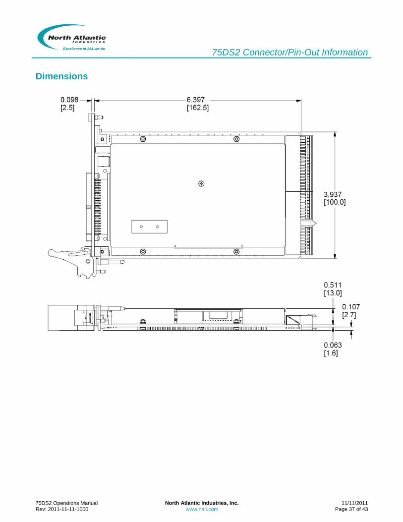
75DS2 Connector/Pin-Out Information
75DS2 Operations Manual North Atlantic Industries, Inc. 11/11/2011 Rev: 2011-11-11-1000 www.naii.com Page 37 of 43
Dimensions

Part Number Designation
75DS2 Operations Manual North Atlantic Industries, Inc. 11/11/2011 Rev: 2011-11-11-1000 www.naii.com Page 38 of 43
PART NUMBER DESIGNATION
75DS2 - XX XX X X X X – XX
SLOT 1 (Enter code – D/S or DLV see module codes) (Enter Z0 if not populated)
SLOT 2 (Enter code – D/S or DLV See module codes) (Enter Z0 if not populated)
ONBOARD REFERENCE SUPPLY (W6, W7) Does not use up a module slot Note 2 0 = No onboard reference module 1 = 2-28Vrms, Programmable onboard reference module 2 = Reserved for future use 3 = 115Vrms Fixed, Programmable onboard reference module
MECHANICAL Note 3
F = Front panel (J4) I/O only P = Rear (J2) I/O only W = P with wedgelocks B = Front panel (J4) and rear (J2) I/O (with front panel sense line connections) Note 4
T = Front panel (J4) and rear (J2) I/O (with rear I/O sense line connections) Note 4
ENVIRONMENTAL C = 0 TO 70°C E = -40 TO +85°C H = E with conformal coating K = C with conformal coating
±12V DC POWER OPTION Note 1 0 = cPCI Power is used 1 = cPCI ±12VDC Power is isolated from PCB power planes. User to connect external power via J4 Front Panel connector
(See Pin-out tables)
CODE (Reserved for special configurations – leave open for standard
Note 1: 12 VDC Power Option
Additional or alternate 12V power pins are available that may be specified at time of order (See part number). The additional
power pins are provided in case the available 12VDC bus power is insufficient for the card configuration. When the factory
installed jumpers are connected, 12VDC power is derived from the backplane power planes. The additional power pins will
now be HOT. When the jumper is disconnected, the card will derive its 12VDC from the external power pins.
Additional/Alternate
Power pins
BUS Power pins Card +/- 12V
PowerFactory set jumper
Factory set jumper configuration:
INSTALLED: +/-12 VDC Power Option “0” (Default)
REMOVED: +/-12 VDC Power Option “1”
Note 2: Only Slot 1 module controls onboard reference supply Note 3: When Rear I/O is specified (mechanical configuration P, W or B) unit cannot be utilized in a PXI chassis.

Part Number Designation
75DS2 Operations Manual North Atlantic Industries, Inc. 11/11/2011 Rev: 2011-11-11-1000 www.naii.com Page 39 of 43
Note 4: Remote sensing is provided for each channel to eliminate errors caused by voltage drops on the interconnecting
cables. The user must connect the load sense connections (i.e. Ch.3- Sense S1) to the respective output signals. Connecting at the load is desirable to mitigate accuracy errors dependent on line and load resistance.

Part Number Designation
75DS2 Operations Manual North Atlantic Industries, Inc. 11/11/2011 Rev: 2011-11-11-1000 www.naii.com Page 40 of 43
Two Channel D/S Module Code Table
*Note: Synchro or Resolver programmability uses a miniature mechanical relay for this task. This capability is not recommended for Military embedded applications. ** There is a +10% tolerance on the upper limit, -0% on the lower limit (i.e. 115V +10%, ∴ 126V Max)
Code Format Output (VL-L) (Vrms)
Ref (VREF) (Vrms)
Frequency (Hz)
Max Load (VA)
NOTES
10 SYN 2 – 28 2 – 115 360 – 1.1K 1.5
11 RSL 2 – 28 2 – 115 360 – 1.1K 1.5
12* PRG S / R 2 – 28 2 – 115 360 – 1.1K 1.5 Programmable, SYN or RSL
13 SYN / RSL 2 – 28 2 – 115 360 – 1.1K 1.5 Channel 1 = SYN, Channel 2 = RSL
14 RSL / SYN 2 – 28 2 – 115 360 – 1.1K 1.5 Channel 1 = RSL, Channel 2 =SYN
15 SYN 2 – 28 2 – 115 47 - 440 1.5
16 RSL 2 – 28 2 – 115 47 - 440 1.5
17* PRG S / R 2 – 28 2 – 115 47 - 440 1.5 Programmable, SYN or RSL
18 SYN / RSL 2 – 28 2 – 115 47 - 440 1.5 Channel 1 = SYN, Channel 2 = RSL
19 RSL / SYN 2 – 28 2 – 115 47 - 440 1.5 Channel 1 = RSL, Channel 2 =SYN
1A RSL 2 – 28 2 – 115 1K – 3K 1.5
1B RSL 2 – 28 2 – 115 3K – 5K 1.5
1C RSL 2 – 28 2 – 115 5K – 7K 1.5
1D RSL 2 – 28 2 – 115 7K – 10K 1.5
1E SYN 2 - 11.8 2 – 115 400 – 1K 1.5
1F SYN 2 - 11.8 2 – 115 47 – 400 1.5
1G SYN 2 - 11.8 2 – 115 1K – 3K 1.5
1H SYN 2 - 11.8 2 – 115 3K – 5K 1.5
1J SYN 2 - 11.8 2 – 115 5K – 7K 1.5
1K SYN 2 - 11.8 2 – 115 7K – 10K 1.5
1L SYN 2 – 28 2 – 115 1K – 3K 1.5
1M SYN 2 – 28 2 – 115 3K – 5K 1.5
1N SYN 2 – 28 2 – 115 5K – 7K 1.5
1P SYN 2 – 28 2 – 115 7K – 10K 1.5
20 SYN 90 2 – 115 360 – 1.1K 2.2
21 RSL 90 2 – 115 360 – 1.1K 2.2
22* PRG S / R 90 2 – 115 360 – 1.1K 2.2 Programmable, SYN or RSL
23 SYN / RSL 90 2 – 115 360 – 1.1K 2.2 Channel 1 = SYN, Channel 2 = RSL
24 RSL / SYN 90 2 – 115 360 – 1.1K 2.2 Channel 1 = RSL, Channel 2 =SYN
25 SYN 90 2 – 115 47 - 440 2.2
26 RSL 90 2 – 115 47 - 440 2.2
27* PRG S / R 90 2 – 115 47 - 440 2.2 Programmable, SYN or RSL
28 SYN / RSL 90 2 – 115 47 - 440 2.2 Channel 1 = SYN, Channel 2 = RSL
29 RSL / SYN 90 2 – 115 47 - 440 2.2 Channel 1 = RSL, Channel 2 =SYN

Part Number Designation
75DS2 Operations Manual North Atlantic Industries, Inc. 11/11/2011 Rev: 2011-11-11-1000 www.naii.com Page 41 of 43
Single Channel D/S Module Code Table
** There is a +10% tolerance on the upper limit, -0% on the lower limit (i.e. 115V +10%, ∴ 126V Max)
Code Format Output (VL-L) (Vrms)
Ref (VREF)** (Vrms)
Frequency (Hz)
Max Load (VA)
30 SYN 11.8 2 – 115 400 – 1K 3.0
31 RSL 2 – 28 2 – 115 400 – 1K 3.0
35 SYN 11.8 2 – 115 47 - 440 3.0
36 RSL 2 – 28 2 – 115 47 - 440 3.0
3A RSL 2 – 28 2 – 115 1K – 3K 3.0
3B RSL 2 – 28 2 – 115 3K – 5K 3.0
3C RSL 2 – 28 2 – 115 5K – 7K 3.0
3D RSL 2 – 28 2 – 115 7K – 10K 3.0
3E SYN 2 - 11.8 2 – 115 1K – 3K 3.0
3F SYN 2 - 11.8 2 – 115 3K – 5K 3.0
3G SYN 2 - 11.8 2 – 115 5K – 7K 3.0
3H SYN 2 - 11.8 2 – 115 7K – 10K 3.0
3J SYN 2 – 28 2 – 115 1K – 3K 3.0
3K SYN 2 – 28 2 – 115 3K – 5K 3.0
3L SYN 2 – 28 2 – 115 5K – 7K 3.0
3M SYN 2 – 28 2 – 115 7K – 10K 3.0
40 SYN 90 2 – 115 400 – 1K 3.0
41 RSL 90 2 – 115 400 – 1K 3.0
45 SYN 90 2 – 115 47 - 440 3.0
46 RSL 90 2 – 115 47 - 440 3.0

Part Number Designation
75DS2 Operations Manual North Atlantic Industries, Inc. 11/11/2011 Rev: 2011-11-11-1000 www.naii.com Page 42 of 43
2/4 Channel DLV Module Code Table
Code Format Output (VL-L) (VRMS)
Ref (VREF)*1 (VRMS)
Frequency*1 (Hz)
Max Load (VA)
50 DLV 2 – 28 2-115 360 – 1.1K 1.5
51 DLV 2 – 28 2-115 47 - 440 1.5
52 DLV 2 – 28 2-115 1K – 3K 1.5
53 DLV 2 – 28 2-115 3K – 5K 1.5
54 DLV 2 – 28 2-115 5K – 7K 1.5
55 DLV 2 – 28 2-115 7K – 10K 1.5
50 DLV 2 – 28 2-115 360 – 1.1K 1.5
51 DLV 2 – 28 2-115 47 - 440 1.5
52 DLV 2 – 28 2-115 1K – 3K 1.5
53 DLV 2 – 28 2-115 3K – 5K 1.5
54 DLV 2 – 28 2-115 5K – 7K 1.5
55 DLV 2 – 28 2-115 7K – 10K 1.5
*1 There is a +10% tolerance on the upper limit, 0% on the lower limit (i.e. 115V +10%)

Revision Page
75DS2 Operations Manual North Atlantic Industries, Inc. 11/11/2011 Rev: 2011-11-11-1000 www.naii.com Page 43 of 43
REVISION PAGE
© 2011 North Atlantic Industries. All rights reserved. This document has been produced for the customers of North Atlantic Industries. Unauthorized use is prohibited without written permission from North Atlantic industries. North Atlantic Industries reserves the right to revise this document to include product updates and may not conform in every aspect to former issues. The information provided in this Operations Manual is believed to be accurate. This document must be reviewed prior to use in the customers’ organizations. No responsibility is assumed by North Atlantic Industries for its use and no licenses or rights are granted by implication or otherwise in connection therewith. North Atlantic Industries recognizes all other trademarks. Trademarks of other products or services mentioned in this document are held by the companies producing them.
Revision Description of Change Engineer Date
2011-11-11-1000 1. G4 Description sub-doc updated/clarified to reference (6) possible
range(s).2. D/S 2CHI Specification sub-doc; corrected minor typo (KHz).3. K9
Specification sub-doc; output characteristics clarified - external VCC source
required for high-side and push-pull drive capability.
LB 11/11/11
2011-10-14-1013 75DS2 Operations Manual Part Number Designation correction to follow
specific designation format (noted rev. 2011-09-28-1442)
LB 10/14/11
2011-09-28-1442 64C2, 64C3, 78C2:CLERICAL CHANGES, UPDATE FORMATTING OF
DOCUMENTS 64CS4: REFORMATTING OF ALL DOCUMENTS 75C2:
REFORMATTING OF ALL DOCUMENTS 75DS2: REFORMATTING OF
ALL DOCUMENTS 78CS2: REFORMATTING OF ALL DOCUMENTS
GL 09/28/11
A4 Updates D/S modules & code tables AS 03/24/10
A3 Added Onboard Reference Supply Register Information AS 04/02/09
A2 Product Configuration page, Correction to front panel connector pinouts
(rotated 180 deg)
AS 12/18/08
A1 Sales Release FR 09/26/08
A Preliminary Specification FR 06/26/08