763934
DESCRIPTION
ÂTRANSCRIPT

Predictive linewidth roughness and CDU simulation using a calibrated physical stochastic resist model
Stewart A. Robertsona, John J. Biaforea, Mark D. Smitha, Michael T. Reillyb,
Jerome Wandellb.
a - KLA-Tencor Corp., FINLE Division, Austin, TX, USA. b - DOW Electronic Materials, Marlborough, MA, USA.
ABSTRACT
A recently developed stochastic resist model, implemented in the PROLITH X3.1 lithography
simulation tool, is fitted to experimental data for a commercially available immersion ArF photoresist, EPIC
2013 (Dow Electronic Materials). Calibration is performed using the mean CD and LWR values through
focus and dose for three line/space features of varying pitch (dense, semi-dense and isolated). An unweighted
Root Mean Squared Error (RMSE) of approximately 1.6 nm is observed when the calibrated model is
compared to the experimental data. Although the model is calibrated only to mean CD and LWR values, it is
able to accurately predict highly accurate CDU distributions at fixed focus and dose conditions for 1D and 2D
(line end shortening) pattern. It is also shown how the stochastic model can be used to describe the bridging
behavior often observed at marginal focus and exposure conditions.
Keywords: Line Edge Roughness (LER), LineWidth Roughness (LWR), Stochastic lithographic modeling,
PROLITH
1. INTRODUCTION
Virtually all lithography simulation used in the semiconductor industry relies on the continuum, or mean-
field, approximation. Such models assume that the exposing illumination can be treated as a series of
interfering plane waves and that the distribution of chemical components within the photoresist (PAG, photo-
acid, quencher etc) is completely homogeneous and can vary continuously. Although this approach ignores
statistical effects, due to the quantization of light into photons and the fact that resist components are discrete
molecules, it has been used successfully for decades to predict core lithographic behaviors. However, as
lithography approaches its fundamental physical limits, phenomena driven by quantized statistical processes,
such as line-edge roughness, contact hole circularity and CD distribution, are becoming increasingly
important. If virtual lithography is to help address these new industry challenges, then simulation tools need
to, at least partially, transition from their current deterministic domain into a probabilistic one.
Advances in Resist Materials and Processing Technology XXVII, edited by Robert D. Allen, Mark H. Somervell, Proc. of SPIE Vol. 7639, 763934 · © 2010 SPIE · CCC code: 0277-786X/10/$18 · doi: 10.1117/12.846539
Proc. of SPIE Vol. 7639 763934-1
Downloaded from SPIE Digital Library on 26 Mar 2010 to 192.146.1.254. Terms of Use: http://spiedl.org/terms

Last year, a stochastic exposure and resist model was proposed [1], the model accurately described
some basic, experimentally observed, lithographic behaviors, specifically mean CD and 3σ LWR through
exposure dose (i.e. exposure latitude) for one photoresist irradiated at two different exposure wavelengths
(ArF and EUV).
In a previous study [2], the same prototype model was calibrated to a comprehensive experimental
data set for a commercially available immersion ArF photoresist, EPIC2013 (Dow Advanced Materials) to
validate its ability to describe other experimentally observed lithographic behaviors, e.g. Focus-Dose CD
response across pitch and CD uniformity (CDU). In this work, we revisit the same calibration data with an
enhanced version of the model (implemented in the commercially available PROLITH X3.1 [KLA Tencor
Corp.]) and compare it against newly collected CDU data for various 2D and 3D mask patterns. This data
comprises of many more repeats than that available in the previous study.
2. STOCHASTIC RESIST MODEL
A conventional continuum or mean-field lithographic model yields the same answer on each trial of
an identical simulation. If the model has been well calibrated this answer will be the average (mean) answer
of many examples of the experiment. A stochastic lithographic model, like real-world experiments, returns a
slightly different answer on each trial, even when the inputs are identical. If the model is correctly calibrated
then the mean value obtained from many simulations should converge with the mean value observed from
many experimental trials and the distribution statistics will be comparable.
The stochastic exposure and resist model used in this work is described in detail by Biafore et al. [1,3]
elsewhere, so there follows only a brief description.
At the start of each simulation trial, the resist volume of interest is populated with PAG and quencher
based on knowledge of their absolute concentrations in the material, using the Monte Carlo Method and
Poisson statistics. During exposure, the photon absorption sites within the resist are determined, again using
Monte Carlo methods. In pure photonic exposure cases, such as ArF immersion lithography, only photons
which are absorbed by PAG molecules are allowed to generate acids, however this reaction is gated by the
quantum efficiency of the PAG, using a further Monte Carlo calculation. Following exposure, the discrete
acid and quencher molecules are propagated through reaction-diffusion-neutralization kinetics during PEB.
Finally, the deprotected latent image in the resist is developed to produce a final relief resist image. Unlike the
output of a continuum model, the resist profile of a stochastic simulation exhibits inherent roughness.
Proc. of SPIE Vol. 7639 763934-2
Downloaded from SPIE Digital Library on 26 Mar 2010 to 192.146.1.254. Terms of Use: http://spiedl.org/terms

At all points in the model the behavior of the PAG, acid, quencher and protection levels are
constrained to obey basic physical laws; conservation of energy, Fickean diffusion, mass balance etc.
The stochastic model used in this work is incorporated in the PROLITH X3.1 simulation package.
The resist model itself has 20 parameters which can be broken into the following categories:
• Absolute PAG loading through the coated resist film
• Absolute quencher loading through the coated resist film
• Optical properties of PAG, quencher and polymer components of the resist
• Exposure kinetics rates
• Acid and quencher diffusivity rates
• PEB reaction kinetics rates
• Development kinetics
If the model described above captures all the relevant first order physics of real-world lithographic resist
processes then it should be able to describe both the observed average behaviors of a given resist and the
observed deviations around that mean. The goal of this study is to test a calibrated stochastic resist model
against experimental data to ensure reasonable agreement is observed.
3. EXPERIMENTAL WORK
Experimental results were generated using an ASML Twinscan /1900 in combination with a TEL
Lithius i+ track system on 300mm wafers. Three duplicate wafers were processed using the following process
conditions:
• BARC: 19 nm Dow AR124 over 79 nm Dow ARC26N
• Resist: Dow EPIC2013 130 nm Resist
100° / 60” SB 100° / 60” PEB 12” GP Nozzle development – Dow MF-26A with FIRM process • Topcoat: 90nm JSR TCX041
90° / 60” Cure • Mask: 6% AttPSM • Exposure Conditions: 1.35NA Immersion, ASML/1900i
0.90σo/0.60σi Annular (X/Y Polarization)
Proc. of SPIE Vol. 7639 763934-3
Downloaded from SPIE Digital Library on 26 Mar 2010 to 192.146.1.254. Terms of Use: http://spiedl.org/terms
Each wafer was exposed using an identical Focus-Exposure Matrix, CD data was collected using a
Hitachi CD SEM for three separate structures, a 50 nm line on a 100 nm pitch, an 80 nm line on a 200 nm
pitch and a 110 nm line on a 700 nm pitch. At each site, the SEM image was captured so that 3σ LWR could
be calculated offline using the SUMMIT LER analysis package (EUV Technology Corp.). The SEM images
were reviewed and all sites which failed due to bridging, scumming, missing features and pattern collapse
were identified. Mean CD values were calculated for those points in the focus-exposure matrices where a
valid CD measurement was obtained on all three wafers and where no imaging failure was observed. A
corresponding average 3σ LWR value was measured for each mean value.
4. STOCHASTIC RESIST MODEL CALIBRATION
The stochastic resist model was calibrated using a mixture of automated optimization and manual
intervention. The absolute PAG and quencher loadings were fixed to the values used in the resist formulation.
Likewise, the optical parameters for the resist components were constrained to their measured values. Only
the exposure, development and reaction-diffusion kinetic parameters were allowed to float.
The merit function used for minimization in the optimization was the unweighted root mean squared
error between mean experimental FEM CD and LWR (3 repeat average) values and the FEM CD and LWR
values (also 3 repeat average) for the three mask features of interest, given by:
RMSE = ( )
11
2
−
−∑=
N
ValueValueN
iiSRMiEXPT
(1)
Where EXPTValue is the mean CD or LWR value from the three wafers for point i, SRMValue is the
mean CD or LWR value from three trials of the Stochastic Resist Model (SRM) for point i and N is double
the number of unique focus-exposure conditions under study. The target FEM data contained the mean CD
and LWR values for all the matrix points which imaged successfully on all three wafers. The final optimized
resist models accuracy can be estimated by comparing the RMSE between the three experimental trials and
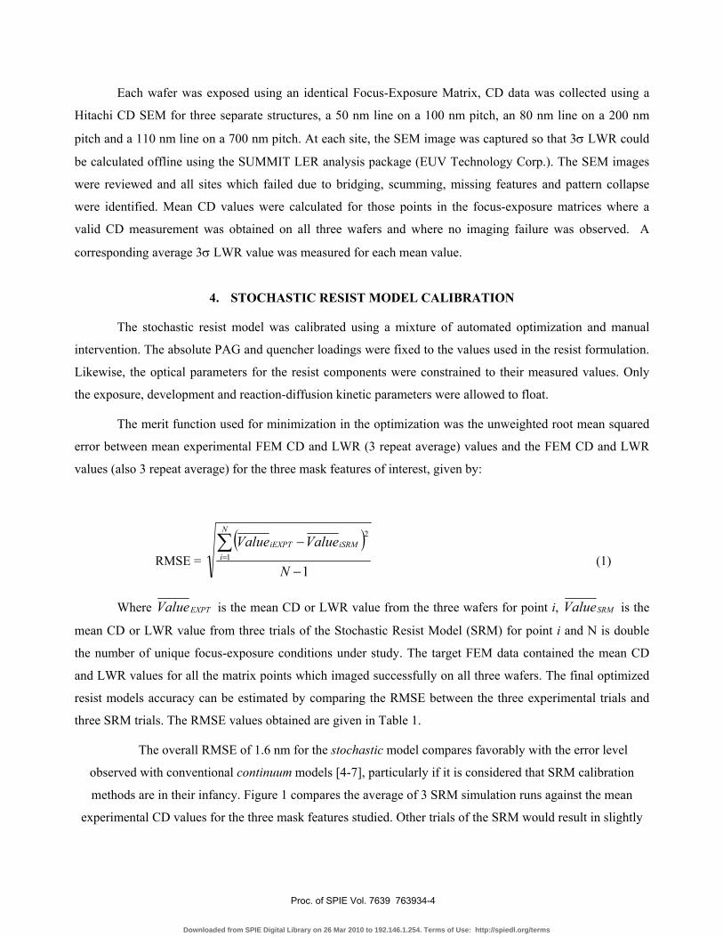
three SRM trials. The RMSE values obtained are given in Table 1.
The overall RMSE of 1.6 nm for the stochastic model compares favorably with the error level
observed with conventional continuum models [4-7], particularly if it is considered that SRM calibration
methods are in their infancy. Figure 1 compares the average of 3 SRM simulation runs against the mean
experimental CD values for the three mask features studied. Other trials of the SRM would result in slightly
Proc. of SPIE Vol. 7639 763934-4
Downloaded from SPIE Digital Library on 26 Mar 2010 to 192.146.1.254. Terms of Use: http://spiedl.org/terms

Figure 1: Bossung plots comparing the average CD of 3 trials of the Stochastic Resist Model against the
mean values obtained from 3 experimental trials. The points are the mean experimental data while the lines
indicate the SRM simulation results.
0
1
2
3
4
5
6
7
8
9
0 0.02 0.04 0.06 0.08 0.1 0.12 0.14 0.16
Defocus (μm)
3 σ L
WR
(nm
)
100nm Pitch Expt100nm Pitch Sim200nm Pitch Expt200nm Pitch Sim700nm Pitch Expt700nm Pitch Sim
Figure 2: Average LWR values of three SRM trials against three experimental trials as a function of
focus value, for the three different pitches studied.
differing answers. Figure 2 compares the average LWR values of three trials of the SRM against the three
experimental trials as a function of focus value for the three different pitches studied.
Proc. of SPIE Vol. 7639 763934-5
Downloaded from SPIE Digital Library on 26 Mar 2010 to 192.146.1.254. Terms of Use: http://spiedl.org/terms
Feature RMSE (CD) RMSE (LWR) Overall RMSE50nm Line, 100nm Pitch 1.7 nm 1.0 nm 1.4 nm80nm Line, 200nm Pitch 2.8 nm 1.1 nm 2.1 nm110nm Line, 700nm Pitch 0.6 nm 0.8 nm 0.7 nm
All 2.0 nm 1.0 nm 1.6 nm
Table 1: RMSE (Root Mean Squared Error) values between calibration data and stochastic resist
model with optimized input parameter values.
5. STOCHASTIC RESIST MODEL PREDICTIONS
In previous studies [2,3] it has been shown that repeated runs of the stochastic resist model under
identical process settings yield slightly different resist profile results. Since these variations are related to
probabilistic statistics, repeated runs can be used to synthetic CDU distributions. If the SRM has been
calibrated well the CDU predictions should correlate well with experimental observations.
In the original EPIC 2013 study [2] only a very limited amount of line-based experimental CDU data
was available. For this work, a much larger number of CD measurements were made and the linewidth data
was augmented with 2D line-end shortening mask patterns.
Each feature of interest was measured 155 times comprising of 31 sites on 5 different wafers. The
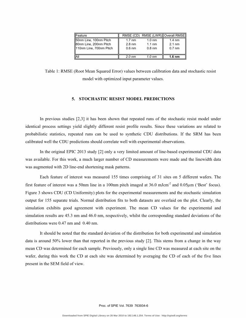
first feature of interest was a 50nm line in a 100nm pitch imaged at 36.0 mJcm-2 and 0.05μm (‘Best’ focus).
Figure 3 shows CDU (CD Uniformity) plots for the experimental measurements and the stochastic simulation
output for 155 separate trials. Normal distribution fits to both datasets are overlaid on the plot. Clearly, the
simulation exhibits good agreement with experiment. The mean CD values for the experimental and
simulation results are 45.3 nm and 46.0 nm, respectively, whilst the corresponding standard deviations of the
distributions were 0.47 nm and 0.40 nm.
It should be noted that the standard deviation of the distribution for both experimental and simulation
data is around 50% lower than that reported in the previous study [2]. This stems from a change in the way
mean CD was determined for each sample. Previously, only a single line CD was measured at each site on the
wafer, during this work the CD at each site was determined by averaging the CD of each of the five lines
present in the SEM field of view.
Proc. of SPIE Vol. 7639 763934-6
Downloaded from SPIE Digital Library on 26 Mar 2010 to 192.146.1.254. Terms of Use: http://spiedl.org/terms
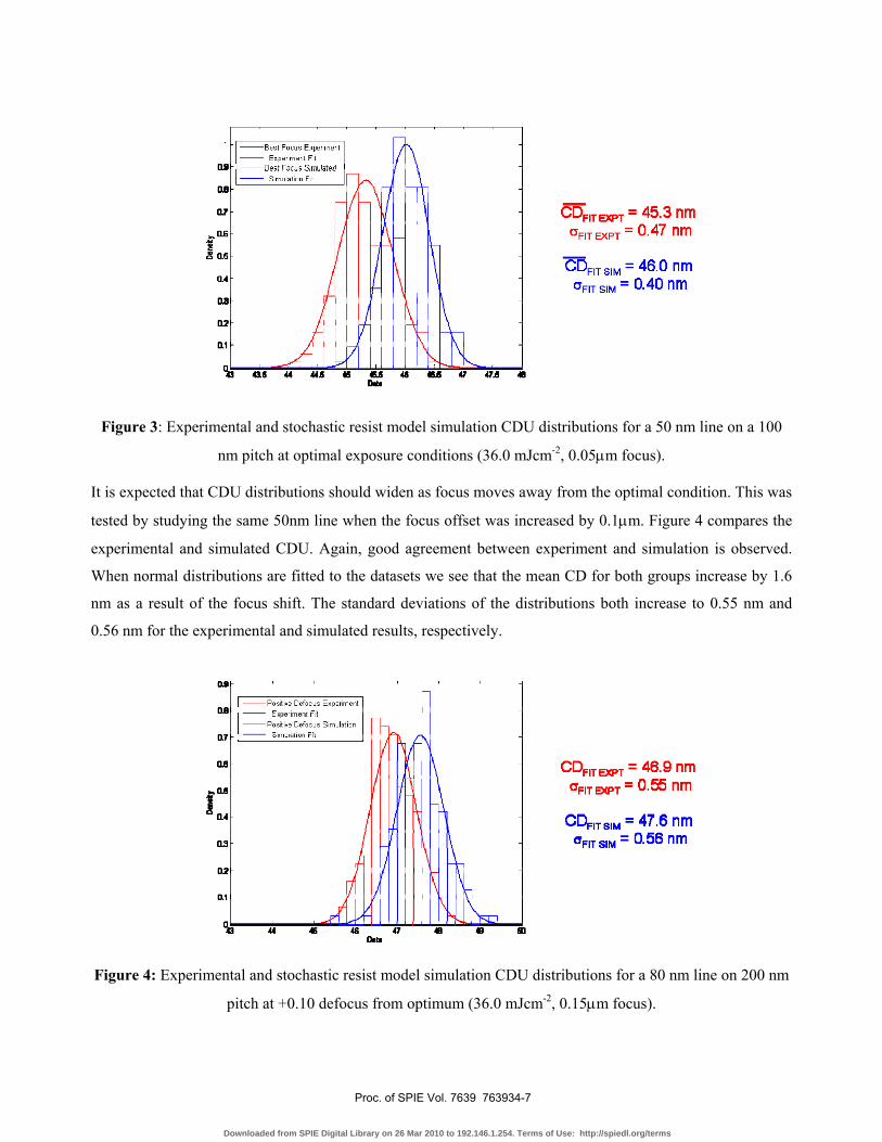
Figure 3: Experimental and stochastic resist model simulation CDU distributions for a 50 nm line on a 100
nm pitch at optimal exposure conditions (36.0 mJcm-2, 0.05μm focus).
It is expected that CDU distributions should widen as focus moves away from the optimal condition. This was
tested by studying the same 50nm line when the focus offset was increased by 0.1μm. Figure 4 compares the
experimental and simulated CDU. Again, good agreement between experiment and simulation is observed.
When normal distributions are fitted to the datasets we see that the mean CD for both groups increase by 1.6
nm as a result of the focus shift. The standard deviations of the distributions both increase to 0.55 nm and
0.56 nm for the experimental and simulated results, respectively.
Figure 4: Experimental and stochastic resist model simulation CDU distributions for a 80 nm line on 200 nm
pitch at +0.10 defocus from optimum (36.0 mJcm-2, 0.15μm focus).
Proc. of SPIE Vol. 7639 763934-7
Downloaded from SPIE Digital Library on 26 Mar 2010 to 192.146.1.254. Terms of Use: http://spiedl.org/terms

After seeing good CDU correlation for 1D mask features (i.e. long lines) the ability of the SRM to
predict more complex 2D patterns was studied. The available reticle had a variety of Line-End Shortening
(LES) patterns available on it. These consisted of gaps of varying length in the center line of a dense array of
50nm lines in a 100nm pitch. The gaps chosen for use were 100nm, 150nm and 250nm, the precise mask
layouts are illustrated in Figures 5, 6 and 7, respectively. Experimentally and within simulation the printed
gap length was measured for 155 sites for each case. The observed distributions with accompanying mean
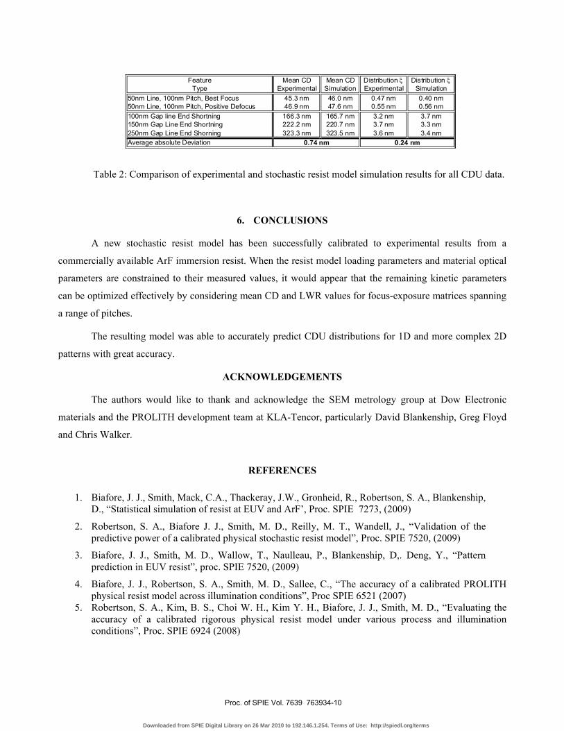
value and distribution statistics are detailed in Table 2 and Figures 5 – 7.
Inspection of the data, shows that in all three cases the model predicts the experimentally observed
mean CD with high accuracy, the observed mismatch ranges from 0.2 nm to 1.5 nm. Similarly, the
distribution widths (represented by the standard deviation of the normal fits) are accurately predicted, with the
absolute average deviation between experiment and simulation spanning the range 0.2 nm – 0.5 nm. As
expected, the distribution widths for the 2D patterns are much larger than those for the linewidth
measurements. The behavior being clearly observed in both experimental and simulation results.
Figure 5: Experimental and stochastic resist model simulation CDU distributions for the 100 nm line-
end shortening pattern optimal exposure conditions (36.0 mJcm-2, 0.05μm focus). The mask layout and a
representative SEM and stochastic resist model simulation are shown for reference.
Proc. of SPIE Vol. 7639 763934-8
Downloaded from SPIE Digital Library on 26 Mar 2010 to 192.146.1.254. Terms of Use: http://spiedl.org/terms
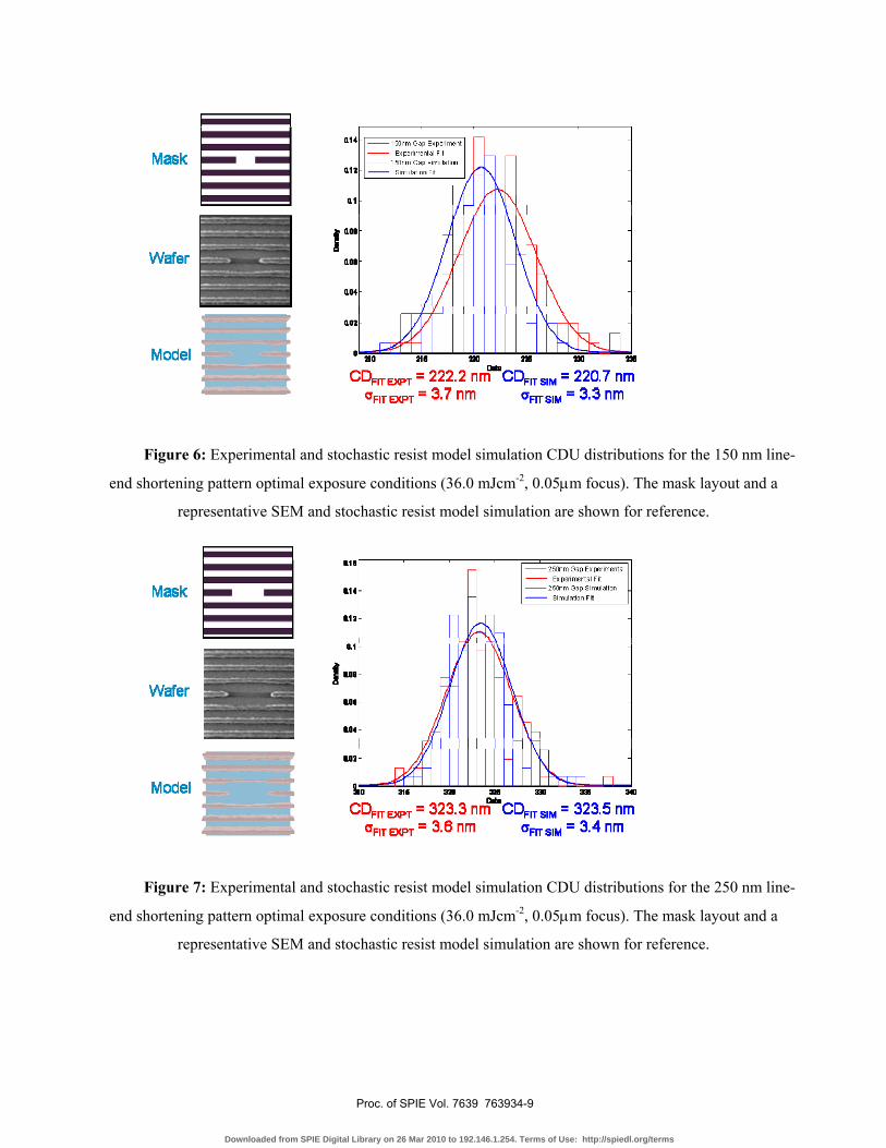
Figure 6: Experimental and stochastic resist model simulation CDU distributions for the 150 nm line-
end shortening pattern optimal exposure conditions (36.0 mJcm-2, 0.05μm focus). The mask layout and a
representative SEM and stochastic resist model simulation are shown for reference.
Figure 7: Experimental and stochastic resist model simulation CDU distributions for the 250 nm line-
end shortening pattern optimal exposure conditions (36.0 mJcm-2, 0.05μm focus). The mask layout and a
representative SEM and stochastic resist model simulation are shown for reference.
Proc. of SPIE Vol. 7639 763934-9
Downloaded from SPIE Digital Library on 26 Mar 2010 to 192.146.1.254. Terms of Use: http://spiedl.org/terms
Feature Mean CD Mean CD Distribution ξ Distribution ξType Experimental Simulation Experimental Simulation
50nm Line, 100nm Pitch, Best Focus 45.3 nm 46.0 nm 0.47 nm 0.40 nm50nm Line, 100nm Pitch, Positive Defocus 46.9 nm 47.6 nm 0.55 nm 0.56 nm100nm Gap line End Shortning 166.3 nm 165.7 nm 3.2 nm 3.7 nm150nm Gap Line End Shortning 222.2 nm 220.7 nm 3.7 nm 3.3 nm250nm Gap Line End Shorning 323.3 nm 323.5 nm 3.6 nm 3.4 nmAverage absolute Deviation 0.74 nm 0.24 nm
Table 2: Comparison of experimental and stochastic resist model simulation results for all CDU data.
6. CONCLUSIONS
A new stochastic resist model has been successfully calibrated to experimental results from a
commercially available ArF immersion resist. When the resist model loading parameters and material optical
parameters are constrained to their measured values, it would appear that the remaining kinetic parameters
can be optimized effectively by considering mean CD and LWR values for focus-exposure matrices spanning
a range of pitches.
The resulting model was able to accurately predict CDU distributions for 1D and more complex 2D
patterns with great accuracy.
ACKNOWLEDGEMENTS
The authors would like to thank and acknowledge the SEM metrology group at Dow Electronic
materials and the PROLITH development team at KLA-Tencor, particularly David Blankenship, Greg Floyd
and Chris Walker.
REFERENCES
1. Biafore, J. J., Smith, Mack, C.A., Thackeray, J.W., Gronheid, R., Robertson, S. A., Blankenship,
D., “Statistical simulation of resist at EUV and ArF’, Proc. SPIE 7273, (2009)
2. Robertson, S. A., Biafore J. J., Smith, M. D., Reilly, M. T., Wandell, J., “Validation of the predictive power of a calibrated physical stochastic resist model”, Proc. SPIE 7520, (2009)
3. Biafore, J. J., Smith, M. D., Wallow, T., Naulleau, P., Blankenship, D,. Deng, Y., “Pattern prediction in EUV resist”, proc. SPIE 7520, (2009)
4. Biafore, J. J., Robertson, S. A., Smith, M. D., Sallee, C., “The accuracy of a calibrated PROLITH physical resist model across illumination conditions”, Proc SPIE 6521 (2007)
5. Robertson, S. A., Kim, B. S., Choi W. H., Kim Y. H., Biafore, J. J., Smith, M. D., “Evaluating the accuracy of a calibrated rigorous physical resist model under various process and illumination conditions”, Proc. SPIE 6924 (2008)
Proc. of SPIE Vol. 7639 763934-10
Downloaded from SPIE Digital Library on 26 Mar 2010 to 192.146.1.254. Terms of Use: http://spiedl.org/terms

6. Yong, L. H., Chun C. L., Chaing-Lin S., Biafore J. J., Roberson S. A., “Advantages of a calibrated physical resist model for pattern prediction”, Proc. SPIE 6923 (2008)
7. Vasek, J. E., Chin-Min, Y., Biafore J. J., Robertson, S. A., “Site portability and extrapolative accuracy of a predictive resist model”, Proc SPIE 6925, (2008)
Proc. of SPIE Vol. 7639 763934-11
Downloaded from SPIE Digital Library on 26 Mar 2010 to 192.146.1.254. Terms of Use: http://spiedl.org/terms