8-bit atmel microcontroller with 16/32/64/128k bytes in...
TRANSCRIPT

ATmega164A/164PA/324A/324PA/644A/644PA/1284/1284P
8-bit Atmel Microcontroller with 16/32/64/128K BytesIn-System Programmable Flash
DATASHEET SUMMARY
Features
High-performance, low-power 8-bit Atmel® AVR® Microcontroller
Advanced RISC architecture 131 powerful Instructions – most single-clock cycle execution
32 × 8 general purpose working registers
Fully static operation
Up to 20MIPS throughput at 20MHz
On-chip 2-cycle multiplier
High endurance non-volatile memory segments 16/32/64/128KBytes of In-System Self-programmable Flash program memory
512/1K/2K/4KBytes EEPROM
1/2/4/16KBytes Internal SRAM
Write/Erase Cycles: 10,000 Flash/ 100,000 EEPROM
Data retention: 20 years at 85°C/ 100 years at 25°C(1)
Optional Boot Code Section with Independent Lock Bits In-System Programming by On-chip Boot Program True Read-While-Write Operation
Programming Lock for Software Security
Atmel QTouch® library support Capacitive touch buttons, sliders and wheels
QTouch and QMatrix acquisition
Up to 64 sense channels
JTAG (IEEE std. 1149.1 Compliant) Interface Boundary-scan Capabilities According to the JTAG Standard
Extensive On-chip Debug Support
Programming of Flash, EEPROM, Fuses, and Lock Bits through the JTAG Interface
Peripheral Features Two 8-bit Timer/Counters with Separate Prescalers and Compare Modes
One/two 16-bit Timer/Counter with Separate Prescaler, Compare Mode, and Capture Mode
Real Time Counter with Separate Oscillator
Six PWM Channels
8-channel, 10-bit ADC Differential mode with selectable gain at 1×, 10× or 200×
Byte-oriented Two-wire Serial Interface
Two Programmable Serial USART
Master/Slave SPI Serial Interface
Atmel-8272GS-AVR-01/2015

Programmable Watchdog Timer with Separate On-chip Oscillator
On-chip Analog Comparator
Interrupt and Wake-up on Pin Change
Special Microcontroller Features Power-on Reset and Programmable Brown-out Detection
Internal Calibrated RC Oscillator
External and Internal Interrupt Sources
Six Sleep Modes: Idle, ADC Noise Reduction, Power-save, Power-down, Standby and Extended Standby
I/O and Packages 32 Programmable I/O Lines
40-pin PDIP, 44-lead TQFP, 44-pad VQFN/QFN/MLF
44-pad DRQFN– 49-ball VFBGA
Operating Voltages 1.8 - 5.5V
Speed Grades 0 - 4MHz @ 1.8 - 5.5V
0 - 10MHz @ 2.7 - 5.5V
0 - 20MHz @ 4.5 - 5.5V
Power Consumption at 1MHz, 1.8V, 25C Active: 0.4mA
Power-down Mode: 0.1µA
Power-save Mode: 0.6µA (Including 32kHz RTC)
Note: 1. See ”Data retention” on page 9 for details.
2ATmega164A/164PA/324A/324PA/644A/644PA/1284/1284P [DATASHEET SUMMARY]Atmel-8272GS-AVR-01/2015
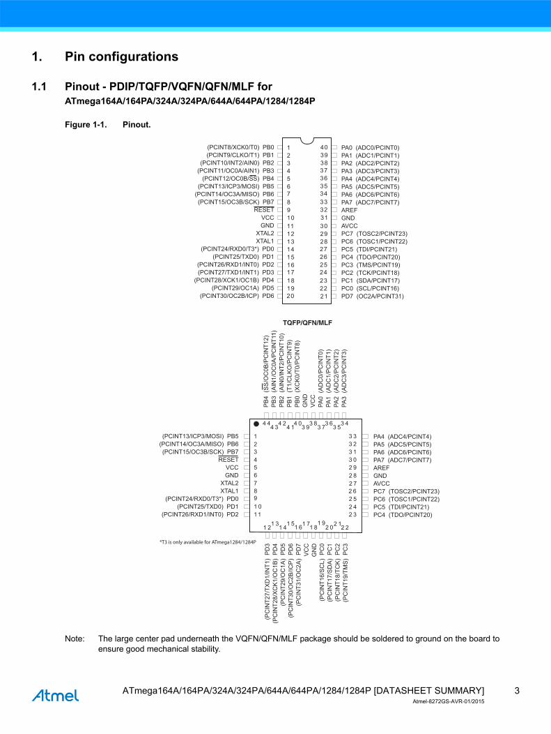
1. Pin configurations
1.1 Pinout - PDIP/TQFP/VQFN/QFN/MLF for ATmega164A/164PA/324A/324PA/644A/644PA/1284/1284P
Figure 1-1. Pinout.
Note: The large center pad underneath the VQFN/QFN/MLF package should be soldered to ground on the board to ensure good mechanical stability.
(PCINT8/XCK0/T0) PB0(PCINT9/CLKO/T1) PB1
(PCINT10/INT2/AIN0) PB2(PCINT11/OC0A/AIN1) PB3
(PCINT12/OC0B/SS) PB4(PCINT13/ICP3/MOSI) PB5
(PCINT14/OC3A/MISO) PB6(PCINT15/OC3B/SCK) PB7
RESETVCCGND
XTAL2XTAL1
(PCINT24/RXD0/T3*) PD0(PCINT25/TXD0) PD1
(PCINT26/RXD1/INT0) PD2(PCINT27/TXD1/INT1) PD3
(PCINT28/XCK1/OC1B) PD4(PCINT29/OC1A) PD5
(PCINT30/OC2B/ICP) PD6
PA0 (ADC0/PCINT0)PA1 (ADC1/PCINT1)PA2 (ADC2/PCINT2)PA3 (ADC3/PCINT3)PA4 (ADC4/PCINT4)PA5 (ADC5/PCINT5)PA6 (ADC6/PCINT6)PA7 (ADC7/PCINT7)AREFGNDAVCCPC7 (TOSC2/PCINT23)PC6 (TOSC1/PCINT22)PC5 (TDI/PCINT21)PC4 (TDO/PCINT20)PC3 (TMS/PCINT19)PC2 (TCK/PCINT18)PC1 (SDA/PCINT17)PC0 (SCL/PCINT16)PD7 (OC2A/PCINT31)
PA4 (ADC4/PCINT4)PA5 (ADC5/PCINT5)PA6 (ADC6/PCINT6)PA7 (ADC7/PCINT7)AREFGNDAVCCPC7 (TOSC2/PCINT23)PC6 (TOSC1/PCINT22)PC5 (TDI/PCINT21)PC4 (TDO/PCINT20)
(PCINT13/ICP3/MOSI) PB5(PCINT14/OC3A/MISO) PB6(PCINT15/OC3B/SCK) PB7
RESETVCCGND
XTAL2XTAL1
(PCINT24/RXD0/T3*) PD0(PCINT25/TXD0) PD1
(PCINT26/RXD1/INT0) PD2
(PC
INT2
7/TX
D1/
INT1
) P
D3
(PC
INT2
8/X
CK
1/O
C1B
) P
D4
(PC
INT2
9/O
C1A
) P
D5
(PC
INT3
0/O
C2B
/ICP
) P
D6
(PC
INT3
1/O
C2A
) P
D7
VC
CG
ND
(PC
INT1
6/S
CL)
PC
0(P
CIN
T17/
SD
A)
PC
1(P
CIN
T18/
TCK
) P
C2
(PC
INT1
9/TM
S)
PC
3
PB
4 (S
S/O
C0B
/PC
INT1
2)P
B3
(AIN
1/O
C0A
/PC
INT1
1)P
B2
(AIN
0/IN
T2/P
CIN
T10)
PB
1 (T
1/C
LKO
/PC
INT9
)P
B0
(XC
K0/
T0/P
CIN
T8)
GN
DV
CC
PA0
(AD
C0/
PC
INT0
)PA
1 (A
DC
1/P
CIN
T1)
PA2
(AD
C2/
PC
INT2
)PA
3 (A
DC
3/P
CIN
T3)
TQFP/QFN/MLF
*T3 is only available for ATmega1284/1284P
3ATmega164A/164PA/324A/324PA/644A/644PA/1284/1284P [DATASHEET SUMMARY]Atmel-8272GS-AVR-01/2015

1.2 Pinout - DRQFN for Atmel ATmega164A/164PA/324A/324PA
Figure 1-2. DRQFN - pinout.
Table 1-1. DRQFN - pinout.
A1 PB5 A7 PD3 A13 PC4 A19 PA3
B1 PB6 B6 PD4 B11 PC5 B16 PA2
A2 PB7 A8 PD5 A14 PC6 A20 PA1
B2 RESET B7 PD6 B12 PC7 B17 PA0
A3 VCC A9 PD7 A15 AVCC A21 VCC
B3 GND B8 VCC B13 GND B18 GND
A4 XTAL2 A10 GND A16 AREF A22 PB0
B4 XTAL1 B9 PC0 B14 PA7 B19 PB1
A5 PD0 A11 PC1 A17 PA6 A23 PB2
B5 PD1 B10 PC2 B15 PA5 B20 PB3
A6 PD2 A12 PC3 A18 PA4 A24 PB4
Top view Bottom view
A1
B1
A2
B2
A3
B3
A4
B4
A5
B5
A6
A18
B15
A17
B14
A16
B13
A15
B12
A14
B11
A13
A12
B1
0
A11
B
9
A10
B
8
A9
B
7
A8
B
6
A7
A24
B2
0
A23
B1
9
A22
B1
8
A21
B1
7
A20
B1
6
A19
A18
B15
A17
B14
A16
B13
A15
B12
A14
B11
A13
A1
B1
A2
B2
A3
B3
A4
B4
A5
B5
A6
A7
B
6
A8
B
7
A9
B
8
A10
B
9
A11
B
10
A12
A19
B1
6
A20
B1
7
A21
B1
8
A22
B1
9
A23
B2
0
A24
4ATmega164A/164PA/324A/324PA/644A/644PA/1284/1284P [DATASHEET SUMMARY]Atmel-8272GS-AVR-01/2015
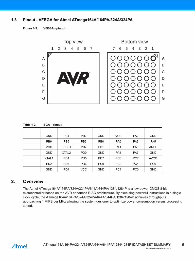
1.3 Pinout - VFBGA for Atmel ATmega164A/164PA/324A/324PA
Figure 1-3. VFBGA - pinout.
2. Overview
The Atmel ATmega164A/164PA/324A/324PA/644A/644PA/1284/1284P is a low-power CMOS 8-bit microcontroller based on the AVR enhanced RISC architecture. By executing powerful instructions in a single clock cycle, the ATmega164A/164PA/324A/324PA/644A/644PA/1284/1284P achieves throughputs approaching 1 MIPS per MHz allowing the system designer to optimize power consumption versus processing speed.
Table 1-2. BGA - pinout.
1 2 3 4 5 6 7
A GND PB4 PB2 GND VCC PA2 GND
B PB6 PB5 PB3 PB0 PA0 PA3 PA5
C VCC RESET PB7 PB1 PA1 PA6 AREF
D GND XTAL2 PD0 GND PA4 PA7 GND
E XTAL1 PD1 PD5 PD7 PC5 PC7 AVCC
F PD2 PD3 PD6 PC0 PC2 PC4 PC6
G GND PD4 VCC GND PC1 PC3 GND
A
B
C
D
E
F
G
1 2 3 4 5 6 7
A
B
C
D
E
F
G
7 6 5 4 3 2 1
Top view Bottom view
5ATmega164A/164PA/324A/324PA/644A/644PA/1284/1284P [DATASHEET SUMMARY]Atmel-8272GS-AVR-01/2015

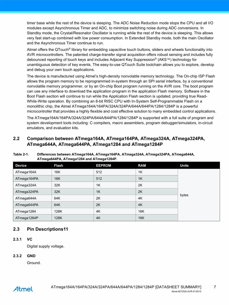
2.1 Block diagram
Figure 2-1. Block diagram.
The AVR core combines a rich instruction set with 32 general purpose working registers. All the 32 registers are directly connected to the Arithmetic Logic Unit (ALU), allowing two independent registers to be accessed in one single instruction executed in one clock cycle. The resulting architecture is more code efficient while achieving throughputs up to ten times faster than conventional CISC microcontrollers.
The Atmel ATmega164A/164PA/324A/324PA/644A/644PA/1284/1284P provide the following features:
16/32/64/128Kbytes of In-System Programmable Flash with Read-While-Write capabilities, 512/1K/2K/4Kbytes EEPROM, 1/2/4/16Kbytes SRAM, 32 general purpose I/O lines, 32 general purpose working registers, Real Time Counter (RTC), three (four for ATmega1284/1284P) flexible Timer/Counters with compare modes and PWM, 2 USARTs, a byte oriented two-wire Serial Interface, a 8-channel, 10-bit ADC with optional differential input stage with programmable gain, programmable Watchdog Timer with Internal Oscillator, an SPI serial port, IEEE std. 1149.1 compliant JTAG test interface, also used for accessing the On-chip Debug system and programming and six software selectable power saving modes. The Idle mode stops the CPU while allowing the SRAM, Timer/Counters, SPI port, and interrupt system to continue functioning. The Power-down mode saves the register contents but freezes the Oscillator, disabling all other chip functions until the next interrupt or Hardware Reset. In Power-save mode, the asynchronous timer continues to run, allowing the user to maintain a
CPU
GND
VCC
RESET
PowerSupervision
POR / BOD &RESET
WatchdogOscillator
WatchdogTimer
OscillatorCircuits /
ClockGeneration
XTAL1
XTAL2
PORT A (8)
PORT D (8)
PD7..0
PORT C (8)
PC5..0
TWI
SPIEEPROM
JTAG/OCD
16bit T/C 1
8bit T/C 2
8bit T/C 0
SRAMFLASH
USART 0
Internal Bandgap reference
Analog Comparator
A/DConverter
PA7..0
PORT B (8)
PB7..0
USART 1
TOSC1/PC6TOSC2/PC7
16bit T/C 1
16bit T/C 3*
* Only available in ATmega1284/1284P
6ATmega164A/164PA/324A/324PA/644A/644PA/1284/1284P [DATASHEET SUMMARY]Atmel-8272GS-AVR-01/2015
timer base while the rest of the device is sleeping. The ADC Noise Reduction mode stops the CPU and all I/O modules except Asynchronous Timer and ADC, to minimize switching noise during ADC conversions. In Standby mode, the Crystal/Resonator Oscillator is running while the rest of the device is sleeping. This allows very fast start-up combined with low power consumption. In Extended Standby mode, both the main Oscillator and the Asynchronous Timer continue to run.
Atmel offers the QTouch® library for embedding capacitive touch buttons, sliders and wheels functionality into AVR microcontrollers. The patented charge-transfer signal acquisition offers robust sensing and includes fully debounced reporting of touch keys and includes Adjacent Key Suppression® (AKS™) technology for unambiguous detection of key events. The easy-to-use QTouch Suite toolchain allows you to explore, develop and debug your own touch applications.
The device is manufactured using Atmel’s high-density nonvolatile memory technology. The On-chip ISP Flash allows the program memory to be reprogrammed in-system through an SPI serial interface, by a conventional nonvolatile memory programmer, or by an On-chip Boot program running on the AVR core. The boot program can use any interface to download the application program in the application Flash memory. Software in the Boot Flash section will continue to run while the Application Flash section is updated, providing true Read-While-Write operation. By combining an 8-bit RISC CPU with In-System Self-Programmable Flash on a monolithic chip, the Atmel ATmega164A/164PA/324A/324PA/644A/644PA/1284/1284P is a powerful microcontroller that provides a highly flexible and cost effective solution to many embedded control applications.
The ATmega164A/164PA/324A/324PA/644A/644PA/1284/1284P is supported with a full suite of program and system development tools including: C compilers, macro assemblers, program debugger/simulators, in-circuit emulators, and evaluation kits.
2.2 Comparison between ATmega164A, ATmega164PA, ATmega324A, ATmega324PA, ATmega644A, ATmega644PA, ATmega1284 and ATmega1284P
2.3 Pin Descriptions11
2.3.1 VC
Digital supply voltage.
2.3.2 GND
Ground.
Table 2-1. Differences between ATmega164A, ATmega164PA, ATmega324A, ATmega324PA, ATmega644A, ATmega644PA, ATmega1284 and ATmega1284P.
Device Flash EEPROM RAM Units
ATmega164A 16K 512 1K
bytes
ATmega164PA 16K 512 1K
ATmega324A 32K 1K 2K
ATmega324PA 32K 1K 2K
ATmega644A 64K 2K 4K
ATmega644PA 64K 2K 4K
ATmega1284 128K 4K 16K
ATmega1284P 128K 4K 16K
7ATmega164A/164PA/324A/324PA/644A/644PA/1284/1284P [DATASHEET SUMMARY]Atmel-8272GS-AVR-01/2015
2.3.3 Port A (PA7:PA0)
Port A serves as analog inputs to the Analog-to-digital Converter.Port A also serves as an 8-bit bi-directional I/O port with internal pull-up resistors (selected for each bit). The Port A output buffers have symmetrical drive characteristics with both high sink and source capability. As inputs, Port A pins that are externally pulled low will source current if the pull-up resistors are activated. The Port A pins are tri-stated when a reset condition becomes active, even if the clock is not running.Port A also serves the functions of various special features of the Atmel ATmega164A/164PA/324A/324PA/644A/644PA/1284/1284P as listed on page 79.
2.3.4 Port B (PB7:PB0)
Port B is an 8-bit bi-directional I/O port with internal pull-up resistors (selected for each bit). The Port B output buffers have symmetrical drive characteristics with both high sink and source capability. As inputs, Port B pins that are externally pulled low will source current if the pull-up resistors are activated. The Port B pins are tri-stated when a reset condition becomes active, even if the clock is not running.Port B also serves the functions of various special features of the ATmega164A/164PA/324A/324PA/644A/644PA/1284/1284P as listed on page 80.
2.3.5 Port C (PC7:PC0)
Port C is an 8-bit bi-directional I/O port with internal pull-up resistors (selected for each bit). The Port C output buffers have symmetrical drive characteristics with both high sink and source capability. As inputs, Port C pins that are externally pulled low will source current if the pull-up resistors are activated. The Port C pins are tri-stated when a reset condition becomes active, even if the clock is not running.Port C also serves the functions of the JTAG interface, along with special features of the Atmel ATmega164A/164PA/324A/324PA/644A/644PA/1284/1284P as listed on page 83.
2.3.6 Port D (PD7:PD0)
Port D is an 8-bit bi-directional I/O port with internal pull-up resistors (selected for each bit). The Port D output buffers have symmetrical drive characteristics with both high sink and source capability. As inputs, Port D pins that are externally pulled low will source current if the pull-up resistors are activated. The Port D pins are tri-stated when a reset condition becomes active, even if the clock is not running.Port D also serves the functions of various special features of the ATmega164A/164PA/324A/324PA/644A/644PA/1284/1284P as listed on page 86.
2.3.7 RESET
Reset input. A low level on this pin for longer than the minimum pulse length will generate a reset, even if the clock is not running. The minimum pulse length is given in ”” on page 325. Shorter pulses are not guaranteed to generate a reset.
2.3.8 XTAL1
Input to the inverting Oscillator amplifier and input to the internal clock operating circuit.
2.3.9 XTAL2
Output from the inverting Oscillator amplifier.
2.3.10 AVCC
AVCC is the supply voltage pin for Port A and the Analog-to-digital Converter. It should be externally connected to VCC, even if the ADC is not used. If the ADC is used, it should be connected to VCC through a low-pass filter.
2.3.11 AREF
This is the analog reference pin for the Analog-to-digital Converter.
8ATmega164A/164PA/324A/324PA/644A/644PA/1284/1284P [DATASHEET SUMMARY]Atmel-8272GS-AVR-01/2015
3. Resources
A comprehensive set of development tools, application notes and datasheets are available for download on http://www.atmel.com/avr.
4. About code examples
This documentation contains simple code examples that briefly show how to use various parts of the device. Be aware that not all C compiler vendors include bit definitions in the header files and interrupt handling in C is compiler dependent. Please confirm with the C compiler documentation for more details.
The code examples assume that the part specific header file is included before compilation. For I/O registers located in extended I/O map, "IN", "OUT", "SBIS", "SBIC", "CBI", and "SBI" instructions must be replaced with instructions that allow access to extended I/O. Typically "LDS" and "STS" combined with "SBRS", "SBRC", "SBR", and "CBR".
Note: 1.
5. Data retention
Reliability Qualification results show that the projected data retention failure rate is much less than 1 PPM over 20 years at 85°C or 100 years at 25°C.
6. Capacitive touch sensing
The Atmel QTouch Library provides a simple to use solution to realize touch sensitive interfaces on most Atmel AVR microcontrollers. The QTouch Library includes support for the QTouch and QMatrix acquisition methods.
Touch sensing can be added to any application by linking the appropriate Atmel QTouch Library for the AVR Microcontroller. This is done by using a simple set of APIs to define the touch channels and sensors, and then calling the touch sensing API’s to retrieve the channel information and determine the touch sensor states.
The QTouch Library is FREE and downloadable from the Atmel website at the following location: www.atmel.com/qtouchlibrary. For implementation details and other information, refer to the Atmel QTouch Library User Guide - also available for download from the Atmel website.
9ATmega164A/164PA/324A/324PA/644A/644PA/1284/1284P [DATASHEET SUMMARY]Atmel-8272GS-AVR-01/2015
7. Register summary
Address Name Bit 7 Bit 6 Bit 5 Bit 4 Bit 3 Bit 2 Bit 1 Bit 0 Page
(0xFF) Reserved - - - - - - -
(0xFE) Reserved - - - - - - - -
(0xFD) Reserved - - - - - - - -
(0xFC) Reserved - - - - - - - -
(0xFB) Reserved - - - - - - -
(0xFA) Reserved - - - - - - - -
(0xF9) Reserved - - - - - - -
(0xF8) Reserved - - - - - - - -
(0xF7) Reserved - - - - - - - -
(0xF6) Reserved - - - - - - - -
(0xF5) Reserved - - - - - - -
(0xF4) Reserved - - - - - - - -
(0xF3) Reserved - - - - - - - -
(0xF2) Reserved - - - - - - - -
(0xF1) Reserved - - - - - - -
(0xF0) Reserved - - - - - - - -
(0xEF) Reserved - - - - - - -
(0xEE) Reserved - - - - - - - -
(0xED) Reserved - - - - - - - -
(0xEC) Reserved - - - - - - - -
(0xEB) Reserved - - - - - - -
(0xEA) Reserved - - - - - - - -
(0xE9) Reserved - - - - - - - -
(0xE8) Reserved - - - - - - - -
(0xE7) Reserved - - - - - - -
(0xE6) Reserved - - - - - - - -
(0xE5) Reserved - - - - - - - -
(0xE4) Reserved - - - - - - - -
(0xE3) Reserved - - - - - - -
(0xE2) Reserved - - - - - - - -
(0xE1) Reserved - - - - - - -
(0xE0) Reserved - - - - - - -
(0xDF) Reserved - - - - - - - -
(0xDE) Reserved - - - - - - - -
(0xDD) Reserved - - - - - - - -
(0xDC) Reserved - - - - - - -
(0xDB) Reserved - - - - - - - -
(0xDA) Reserved - - - - - - - -
(0xD9) Reserved - - - - - - - -
(0xD8) Reserved - - - - - - - -
(0xD7) Reserved - - - - - - - -
(0xD6) Reserved - - - - - - - -
(0xD5) Reserved - - - - - - - -
(0xD4) Reserved - - - - - - - -
(0xD3) Reserved - - - - - - - -
(0xD2) Reserved - - - - - - - -
(0xD1) Reserved - - - - - - - -
(0xD0) Reserved - - - - - - - -
(0xCF) Reserved - - - - - - - -
(0xCE) UDR1 USART1 I/O Data Register 185
(0xCD) UBRR1H - - - - USART1 Baud Rate Register High Byte 189/202
(0xCC) UBRR1L USART1 Baud Rate Register Low Byte 189/202
(0xCB) Reserved - - - - - - - -
(0xCA) UCSR1C UMSEL11 UMSEL10 UPM11 UPM10 USBS1 UCSZ11/UDORD0(5) UCSZ10/UCPHA0(5) UCPOL1 187/201
(0xC9) UCSR1B RXCIE1 TXCIE1 UDRIE1 RXEN1 TXEN1 UCSZ12 RXB81 TXB81 186/200
(0xC8) UCSR1A RXC1 TXC1 UDRE1 FE1 DOR1 UPE1 U2X1 MPCM1 185/200
(0xC7) Reserved - - - - - - - -
(0xC6) UDR0 USART0 I/O Data Register 185
(0xC5) UBRR0H - - - - USART0 Baud Rate Register High Byte 189/202
(0xC4) UBRR0L USART0 Baud Rate Register Low Byte 189/202
(0xC3) Reserved - - - - - - - -
(0xC2) UCSR0C UMSEL01 UMSEL00 UPM01 UPM00 USBS0 UCSZ01/UDORD0(5) UCSZ00/UCPHA0(5) UCPOL0 187/201
(0xC1) UCSR0B RXCIE0 TXCIE0 UDRIE0 RXEN0 TXEN0 UCSZ02 RXB80 TXB80 186/200
10ATmega164A/164PA/324A/324PA/644A/644PA/1284/1284P [DATASHEET SUMMARY]Atmel-8272GS-AVR-01/2015

(0xC0) UCSR0A RXC0 TXC0 UDRE0 FE0 DOR0 UPE0 U2X0 MPCM0 185/200
(0xBF) Reserved - - - - - - - -
(0xBE) Reserved - - - - - - - -
(0xBD) TWAMR TWAM6 TWAM5 TWAM4 TWAM3 TWAM2 TWAM1 TWAM0 - 231
(0xBC) TWCR TWINT TWEA TWSTA TWSTO TWWC TWEN - TWIE 228
(0xBB) TWDR two-wire Serial Interface Data Register 230
(0xBA) TWAR TWA6 TWA5 TWA4 TWA3 TWA2 TWA1 TWA0 TWGCE 231
(0xB9) TWSR TWS7 TWS6 TWS5 TWS4 TWS3 - TWPS1 TWPS0 229
(0xB8) TWBR two-wire Serial Interface Bit Rate Register 228
(0xB7) Reserved - - - - - - - -
(0xB6) ASSR - EXCLK AS2 TCN2UB OCR2AUB OCR2BUB TCR2AUB TCR2BUB 155
(0xB5) Reserved - - - - - - - -
(0xB4) OCR2B Timer/Counter2 Output Compare Register B 155
(0xB3) OCR2A Timer/Counter2 Output Compare Register A 155
(0xB2) TCNT2 Timer/Counter2 (8 Bit) 154
(0xB1) TCCR2B FOC2A FOC2B - - WGM22 CS22 CS21 CS20 153
(0xB0) TCCR2A COM2A1 COM2A0 COM2B1 COM2B0 - - WGM21 WGM20 151
(0xAF) Reserved - - - - - - - -
(0xAE) Reserved - - - - - - - -
(0xAD) Reserved - - - - - - - -
(0xAC) Reserved - - - - - - - -
(0xAB) Reserved - - - - - - - -
(0xAA) Reserved - - - - - - - -
(0xA9) Reserved - - - - - - - -
(0xA8) Reserved - - - - - - - -
(0xA7) Reserved - - - - - - - -
(0xA6) Reserved - - - - - - - -
(0xA5) Reserved - - - - - - - -
(0xA4) Reserved - - - - - - - -
(0xA3) Reserved - - - - - - - -
(0xA2) Reserved - - - - - - - -
(0xA1) Reserved - - - - - - - -
(0xA0) Reserved - - - - - - - -
(0x9F) Reserved - - - - - - - -
(0x9E) Reserved - - - - - - - -
(0x9D) Reserved - - - - - - - -
(0x9C) Reserved - - - - - - - -
(0x9B) OCR3BH Timer/Counter3 - Output Compare Register B High Byte(7) 132
(0x9A) OCR3BL Timer/Counter3 - Output Compare Register B Low Byte(7) 132
(0x99) OCR3AH Timer/Counter3 - Output Compare Register A High Byte(7) 132
(0x98) OCR3AL Timer/Counter3 - Output Compare Register A Low Byte(7) 132
(0x97) ICR3H Timer/Counter3 - Input Capture Register High Byte(7) 133
(0x96) ICR3L Timer/Counter3 - Input Capture Register Low Byte(7) 133
(0x95) TCNT3H Timer/Counter3 - Counter Register High Byte(7) 132
(0x94) TCNT3L Timer/Counter3 - Counter Register Low Byte(7) 132
(0x93) Reserved - - - - - - - -
(0x92) TCCR3C FOC3A FOC3B - - - - - - 131
(0x91) TCCR3B ICNC3 ICES3 - WGM33 WGM32 CS32 CS31 CS30 130
(0x90) TCCR3A COM3A1 COM3A0 COM3B1 COM3B0 - - WGM31 WGM30 128
(0x8F) Reserved - - - - - - - -
(0x8E) Reserved - - - - - - - -
(0x8D) Reserved - - - - - - - -
(0x8C) Reserved - - - - - - - -
(0x8B) OCR1BH Timer/Counter1 - Output Compare Register B High Byte 132
(0x8A) OCR1BL Timer/Counter1 - Output Compare Register B Low Byte 132
(0x89) OCR1AH Timer/Counter1 - Output Compare Register A High Byte 132
(0x88) OCR1AL Timer/Counter1 - Output Compare Register A Low Byte 132
(0x87) ICR1H Timer/Counter1 - Input Capture Register High Byte 133
(0x86) ICR1L Timer/Counter1 - Input Capture Register Low Byte 133
(0x85) TCNT1H Timer/Counter1 - Counter Register High Byte 132
(0x84) TCNT1L Timer/Counter1 - Counter Register Low Byte 132
(0x83) Reserved - - - - - - - -
(0x82) TCCR1C FOC1A FOC1B - - - - - - 131
(0x81) TCCR1B ICNC1 ICES1 - WGM13 WGM12 CS12 CS11 CS10 130
(0x80) TCCR1A COM1A1 COM1A0 COM1B1 COM1B0 - - WGM11 WGM10 128
(0x7F) DIDR1 - - - - - - AIN1D AIN0D 234
(0x7E) DIDR0 ADC7D ADC6D ADC5D ADC4D ADC3D ADC2D ADC1D ADC0D 253
(0x7D) Reserved - - - - - - - -
Address Name Bit 7 Bit 6 Bit 5 Bit 4 Bit 3 Bit 2 Bit 1 Bit 0 Page
11ATmega164A/164PA/324A/324PA/644A/644PA/1284/1284P [DATASHEET SUMMARY]Atmel-8272GS-AVR-01/2015
(0x7C) ADMUX REFS1 REFS0 ADLAR MUX4 MUX3 MUX2 MUX1 MUX0 249
(0x7B) ADCSRB - ACME - - - ADTS2 ADTS1 ADTS0 233
(0x7A) ADCSRA ADEN ADSC ADATE ADIF ADIE ADPS2 ADPS1 ADPS0 250
(0x79) ADCH ADC Data Register High byte 251
(0x78) ADCL ADC Data Register Low byte 251
(0x77) Reserved - - - - - - - -
(0x76) Reserved - - - - - - - -
(0x75) Reserved - - - - - - - -
(0x74) Reserved - - - - - - - -
(0x73) PCMSK3 PCINT31 PCINT30 PCINT29 PCINT28 PCINT27 PCINT26 PCINT25 PCINT24 70
(0x72) Reserved - - - - - - - -
(0x71) TIMSK3 - - ICIE3 - - OCIE3B OCIE3A TOIE3 134
(0x70) TIMSK2 - - - - - OCIE2B OCIE2A TOIE2 156
(0x6F) TIMSK1 - - ICIE1 - - OCIE1B OCIE1A TOIE1 134
(0x6E) TIMSK0 - - - - - OCIE0B OCIE0A TOIE0 105
(0x6D) PCMSK2 PCINT23 PCINT22 PCINT21 PCINT20 PCINT19 PCINT18 PCINT17 PCINT16 70
(0x6C) PCMSK1 PCINT15 PCINT14 PCINT13 PCINT12 PCINT11 PCINT10 PCINT9 PCINT8 70
(0x6B) PCMSK0 PCINT7 PCINT6 PCINT5 PCINT4 PCINT3 PCINT2 PCINT1 PCINT0 71
(0x6A) Reserved - - - - - - - -
(0x69) EICRA - - ISC21 ISC20 ISC11 ISC10 ISC01 ISC00 67
(0x68) PCICR - - - - PCIE3 PCIE2 PCIE1 PCIE0 69
(0x67) Reserved - - - - - - - -
(0x66) OSCCAL Oscillator Calibration Register 40
(0x65) PRR1 - - - - - - - --PRTIM3 49
(0x64) PRR0 PRTWI PRTIM2 PRTIM0 PRUSART1 PRTIM1 PRSPI PRUSART0 PRADC 48
(0x63) Reserved - - - - - - - -
(0x62) Reserved - - - - - - - -
(0x61) CLKPR CLKPCE - - - CLKPS3 CLKPS2 CLKPS1 CLKPS0 40
(0x60) WDTCSR WDIF WDIE WDP3 WDCE WDE WDP2 WDP1 WDP0 59
0x3F (0x5F) SREG I T H S V N Z C 11
0x3E (0x5E) SPH SP15 SP14 SP13 SP12 SP11 SP10 SP9 SP8 12
0x3D (0x5D) SPL SP7 SP6 SP5 SP4 SP3 SP2 SP1 SP0 12
0x3C (0x5C) Reserved - - - - - - - -
0x3B (0x5B) Reserved - - - - - - - -
0x3A (0x5A) Reserved - - - - - - - -
0x39 (0x59) Reserved - - - - - - - -
0x38 (0x58) Reserved - - - - - - - -
0x37 (0x57) SPMCSR SPMIE RWWSB SIGRD RWWSRE BLBSET PGWRT PGERS SPMEN 285
0x36 (0x56) Reserved - - - - - - - -
0x35 (0x55) MCUCR JTD BODS(6) BODSE(6) PUD - - IVSEL IVCE 89/268
0x34 (0x54) MCUSR - - - JTRF WDRF BORF EXTRF PORF 58/268
0x33 (0x53) SMCR - - - - SM2 SM1 SM0 SE 47
0x32 (0x52) Reserved - - - - - - - -
0x31 (0x51) OCDR On-Chip Debug Register 259
0x30 (0x50) ACSR ACD ACBG ACO ACI ACIE ACIC ACIS1 ACIS0 250
0x2F (0x4F) Reserved - - - - - - - -
0x2E (0x4E) SPDR SPI 0 Data Register 166
0x2D (0x4D) SPSR SPIF0 WCOL0 - - - - - SPI2X0 165
0x2C (0x4C) SPCR SPIE0 SPE0 DORD0 MSTR0 CPOL0 CPHA0 SPR01 SPR00 164
0x2B (0x4B) GPIOR2 General Purpose I/O Register 2 29
0x2A (0x4A) GPIOR1 General Purpose I/O Register 1 29
0x29 (0x49) Reserved - - - - - - - -
0x28 (0x48) OCR0B Timer/Counter0 Output Compare Register B 105
0x27 (0x47) OCR0A Timer/Counter0 Output Compare Register A 105
0x26 (0x46) TCNT0 Timer/Counter0 (8 Bit) 105
0x25 (0x45) TCCR0B FOC0A FOC0B - - WGM02 CS02 CS01 CS00 104
0x24 (0x44) TCCR0A COM0A1 COM0A0 COM0B1 COM0B0 - - WGM01 WGM00 105
0x23 (0x43) GTCCR TSM - - - - - PSRASY PSRSYNC 157
0x22 (0x42) EEARH - - - - EEPROM Address Register High Byte 24
0x21 (0x41) EEARL EEPROM Address Register Low Byte 24
0x20 (0x40) EEDR EEPROM Data Register 24
0x1F (0x3F) EECR - - EEPM1 EEPM0 EERIE EEMPE EEPE EERE 24
0x1E (0x3E) GPIOR0 General Purpose I/O Register 0 29
0x1D (0x3D) EIMSK - - - - - INT2 INT1 INT0 68
0x1C (0x3C) EIFR - - - - - INTF2 INTF1 INTF0 68
0x1B (0x3B) PCIFR - - - - PCIF3 PCIF2 PCIF1 PCIF0 69
0x1A (0x3A) Reserved - - - - - - - -
0x19 (0x39) Reserved - - - - - - - -
Address Name Bit 7 Bit 6 Bit 5 Bit 4 Bit 3 Bit 2 Bit 1 Bit 0 Page
12ATmega164A/164PA/324A/324PA/644A/644PA/1284/1284P [DATASHEET SUMMARY]Atmel-8272GS-AVR-01/2015

Notes: 1. For compatibility with future devices, reserved bits should be written to zero if accessed. Reserved I/O memory addresses should never be written.
2. I/O registers within the address range $00 - $1F are directly bit-accessible using the SBI and CBI instructions. In these registers, the value of single bits can be checked by using the SBIS and SBIC instructions.
3. Some of the status flags are cleared by writing a logical one to them. Note that the CBI and SBI instructions will operate on all bits in the I/O register, writing a one back into any flag read as set, thus clearing the flag. The CBI and SBI instructions work with registers 0x00 to 0x1F only.
4. When using the I/O specific commands IN and OUT, the I/O addresses $00 - $3F must be used. When addressing I/O registers as data space using LD and ST instructions, $20 must be added to these addresses. The ATmega164A/164PA/324A/324PA/644A/644PA/1284/1284P is a complex microcontroller with more peripheral units than can be supported within the 64 location reserved in Opcode for the IN and OUT instructions. For the Extended I/O space from $60 - $FF, only the ST/STS/STD and LD/LDS/LDD instructions can be used.
5. USART in SPI Master Mode.
6. Only available in the ATmega164PA/324PA/644PA/1284P.
7. Only available in the ATmega1284/1284P
0x18 (0x38) TIFR3 - - ICF3 - - OCF3B OCF3A TOV3 136
0x17 (0x37) TIFR2 - - - - - OCF2B OCF2A TOV2 156
0x16 (0x36) TIFR1 - - ICF1 - - OCF1B OCF1A TOV1 135
0x15 (0x35) TIFR0 - - - - - OCF0B OCF0A TOV0 106
0x14 (0x34) Reserved - - - - - - - -
0x13 (0x33) Reserved - - - - - - - -
0x12 (0x32) Reserved - - - - - - - -
0x11 (0x31) Reserved - - - - - - - -
0x10 (0x30) Reserved - - - - - - - -
0x0F (0x2F) Reserved - - - - - - - -
0x0E (0x2E) Reserved - - - - - - - -
0x0D (0x2D) Reserved - - - - - - - -
0x0C (0x2C) Reserved - - - - - - - -
0x0B (0x2B) PORTD PORTD7 PORTD6 PORTD5 PORTD4 PORTD3 PORTD2 PORTD1 PORTD0 90
0x0A (0x2A) DDRD DDD7 DDD6 DDD5 DDD4 DDD3 DDD2 DDD1 DDD0 90
0x09 (0x29) PIND PIND7 PIND6 PIND5 PIND4 PIND3 PIND2 PIND1 PIND0 90
0x08 (0x28) PORTC PORTC7 PORTC6 PORTC5 PORTC4 PORTC3 PORTC2 PORTC1 PORTC0 90
0x07 (0x27) DDRC DDC7 DDC6 DDC5 DDC4 DDC3 DDC2 DDC1 DDC0 90
0x06 (0x26) PINC PINC7 PINC6 PINC5 PINC4 PINC3 PINC2 PINC1 PINC0 90
0x05 (0x25) PORTB PORTB7 PORTB6 PORTB5 PORTB4 PORTB3 PORTB2 PORTB1 PORTB0 89
0x04 (0x24) DDRB DDB7 DDB6 DDB5 DDB4 DDB3 DDB2 DDB1 DDB0 89
0x03 (0x23) PINB PINB7 PINB6 PINB5 PINB4 PINB3 PINB2 PINB1 PINB0 90
0x02 (0x22) PORTA PORTA7 PORTA6 PORTA5 PORTA4 PORTA3 PORTA2 PORTA1 PORTA0 89
0x01 (0x21) DDRA DDA7 DDA6 DDA5 DDA4 DDA3 DDA2 DDA1 DDA0 89
0x00 (0x20) PINA PINA7 PINA6 PINA5 PINA4 PINA3 PINA2 PINA1 PINA0 89
Address Name Bit 7 Bit 6 Bit 5 Bit 4 Bit 3 Bit 2 Bit 1 Bit 0 Page
13ATmega164A/164PA/324A/324PA/644A/644PA/1284/1284P [DATASHEET SUMMARY]Atmel-8272GS-AVR-01/2015

8. Instruction set summary
Mnemonics Operands Description Operation Flags #Clocks
ARITHMETIC AND LOGIC INSTRUCTIONS
ADD Rd, Rr Add two Registers Rd Rd + Rr Z,C,N,V,H 1
ADC Rd, Rr Add with Carry two Registers Rd Rd + Rr + C Z,C,N,V,H 1
ADIW Rdl,K Add Immediate to Word Rdh:Rdl Rdh:Rdl + K Z,C,N,V,S 2
SUB Rd, Rr Subtract two Registers Rd Rd - Rr Z,C,N,V,H 1
SUBI Rd, K Subtract Constant from Register Rd Rd - K Z,C,N,V,H 1
SBC Rd, Rr Subtract with Carry two Registers Rd Rd - Rr - C Z,C,N,V,H 1
SBCI Rd, K Subtract with Carry Constant from Reg. Rd Rd - K - C Z,C,N,V,H 1
SBIW Rdl,K Subtract Immediate from Word Rdh:Rdl Rdh:Rdl - K Z,C,N,V,S 2
AND Rd, Rr Logical AND Registers Rd Rd Rr Z,N,V 1
ANDI Rd, K Logical AND Register and Constant Rd Rd K Z,N,V 1
OR Rd, Rr Logical OR Registers Rd Rd v Rr Z,N,V 1
ORI Rd, K Logical OR Register and Constant Rd Rd v K Z,N,V 1
EOR Rd, Rr Exclusive OR Registers Rd Rd Rr Z,N,V 1
COM Rd One’s Complement Rd 0xFF Rd Z,C,N,V 1
NEG Rd Two’s Complement Rd 0x00 Rd Z,C,N,V,H 1
SBR Rd,K Set Bit(s) in Register Rd Rd v K Z,N,V 1
CBR Rd,K Clear Bit(s) in Register Rd Rd (0xFF - K) Z,N,V 1
INC Rd Increment Rd Rd + 1 Z,N,V 1
DEC Rd Decrement Rd Rd 1 Z,N,V 1
TST Rd Test for Zero or Minus Rd Rd Rd Z,N,V 1
CLR Rd Clear Register Rd Rd Rd Z,N,V 1
SER Rd Set Register Rd 0xFF None 1
MUL Rd, Rr Multiply Unsigned R1:R0 Rd x Rr Z,C 2
MULS Rd, Rr Multiply Signed R1:R0 Rd x Rr Z,C 2
MULSU Rd, Rr Multiply Signed with Unsigned R1:R0 Rd x Rr Z,C 2
FMUL Rd, Rr Fractional Multiply Unsigned R1:R0 (Rd x Rr) << 1 Z,C 2
FMULS Rd, Rr Fractional Multiply Signed R1:R0 (Rd x Rr) << 1 Z,C 2
FMULSU Rd, Rr Fractional Multiply Signed with Unsigned R1:R0 (Rd x Rr) << 1 Z,C 2
BRANCH INSTRUCTIONS
RJMP k Relative Jump PC PC + k + 1 None 2
IJMP Indirect Jump to (Z) PC Z None 2
JMP k Direct Jump PC k None 3
RCALL k Relative Subroutine Call PC PC + k + 1 None 3
ICALL Indirect Call to (Z) PC Z None 3
CALL k Direct Subroutine Call PC k None 4
RET Subroutine Return PC STACK None 4
RETI Interrupt Return PC STACK I 4
CPSE Rd,Rr Compare, Skip if Equal if (Rd = Rr) PC PC + 2 or 3 None 1/2/3
CP Rd,Rr Compare Rd Rr Z, N,V,C,H 1
CPC Rd,Rr Compare with Carry Rd Rr C Z, N,V,C,H 1
CPI Rd,K Compare Register with Immediate Rd K Z, N,V,C,H 1
SBRC Rr, b Skip if Bit in Register Cleared if (Rr(b)=0) PC PC + 2 or 3 None 1/2/3
SBRS Rr, b Skip if Bit in Register is Set if (Rr(b)=1) PC PC + 2 or 3 None 1/2/3
SBIC P, b Skip if Bit in I/O Register Cleared if (P(b)=0) PC PC + 2 or 3 None 1/2/3
SBIS P, b Skip if Bit in I/O Register is Set if (P(b)=1) PC PC + 2 or 3 None 1/2/3
BRBS s, k Branch if Status Flag Set if (SREG(s) = 1) then PCPC+k + 1 None 1/2
BRBC s, k Branch if Status Flag Cleared if (SREG(s) = 0) then PCPC+k + 1 None 1/2
BREQ k Branch if Equal if (Z = 1) then PC PC + k + 1 None 1/2
BRNE k Branch if Not Equal if (Z = 0) then PC PC + k + 1 None 1/2
BRCS k Branch if Carry Set if (C = 1) then PC PC + k + 1 None 1/2
BRCC k Branch if Carry Cleared if (C = 0) then PC PC + k + 1 None 1/2
BRSH k Branch if Same or Higher if (C = 0) then PC PC + k + 1 None 1/2
BRLO k Branch if Lower if (C = 1) then PC PC + k + 1 None 1/2
BRMI k Branch if Minus if (N = 1) then PC PC + k + 1 None 1/2
BRPL k Branch if Plus if (N = 0) then PC PC + k + 1 None 1/2
BRGE k Branch if Greater or Equal, Signed if (N V= 0) then PC PC + k + 1 None 1/2
BRLT k Branch if Less Than Zero, Signed if (N V= 1) then PC PC + k + 1 None 1/2
BRHS k Branch if Half Carry Flag Set if (H = 1) then PC PC + k + 1 None 1/2
BRHC k Branch if Half Carry Flag Cleared if (H = 0) then PC PC + k + 1 None 1/2
BRTS k Branch if T Flag Set if (T = 1) then PC PC + k + 1 None 1/2
BRTC k Branch if T Flag Cleared if (T = 0) then PC PC + k + 1 None 1/2
BRVS k Branch if Overflow Flag is Set if (V = 1) then PC PC + k + 1 None 1/2
14ATmega164A/164PA/324A/324PA/644A/644PA/1284/1284P [DATASHEET SUMMARY]Atmel-8272GS-AVR-01/2015
BRVC k Branch if Overflow Flag is Cleared if (V = 0) then PC PC + k + 1 None 1/2
BRIE k Branch if Interrupt Enabled if ( I = 1) then PC PC + k + 1 None 1/2
BRID k Branch if Interrupt Disabled if ( I = 0) then PC PC + k + 1 None 1/2
BIT AND BIT-TEST INSTRUCTIONS
SBI P,b Set Bit in I/O Register I/O(P,b) 1 None 2
CBI P,b Clear Bit in I/O Register I/O(P,b) 0 None 2
LSL Rd Logical Shift Left Rd(n+1) Rd(n), Rd(0) 0 Z,C,N,V 1
LSR Rd Logical Shift Right Rd(n) Rd(n+1), Rd(7) 0 Z,C,N,V 1
ROL Rd Rotate Left Through Carry Rd(0)C,Rd(n+1) Rd(n),CRd(7) Z,C,N,V 1
ROR Rd Rotate Right Through Carry Rd(7)C,Rd(n) Rd(n+1),CRd(0) Z,C,N,V 1
ASR Rd Arithmetic Shift Right Rd(n) Rd(n+1), n=0..6 Z,C,N,V 1
SWAP Rd Swap Nibbles Rd(3..0)Rd(7..4),Rd(7..4)Rd(3..0) None 1
BSET s Flag Set SREG(s) 1 SREG(s) 1
BCLR s Flag Clear SREG(s) 0 SREG(s) 1
BST Rr, b Bit Store from Register to T T Rr(b) T 1
BLD Rd, b Bit load from T to Register Rd(b) T None 1
SEC Set Carry C 1 C 1
CLC Clear Carry C 0 C 1
SEN Set Negative Flag N 1 N 1
CLN Clear Negative Flag N 0 N 1
SEZ Set Zero Flag Z 1 Z 1
CLZ Clear Zero Flag Z 0 Z 1
SEI Global Interrupt Enable I 1 I 1
CLI Global Interrupt Disable I 0 I 1
SES Set Signed Test Flag S 1 S 1
CLS Clear Signed Test Flag S 0 S 1
SEV Set Twos Complement Overflow. V 1 V 1
CLV Clear Twos Complement Overflow V 0 V 1
SET Set T in SREG T 1 T 1
CLT Clear T in SREG T 0 T 1
SEH Set Half Carry Flag in SREG H 1 H 1
CLH Clear Half Carry Flag in SREG H 0 H 1
DATA TRANSFER INSTRUCTIONS
MOV Rd, Rr Move Between Registers Rd Rr None 1
MOVW Rd, Rr Copy Register Word Rd+1:Rd Rr+1:Rr None 1
LDI Rd, K Load Immediate Rd K None 1
LD Rd, X Load Indirect Rd (X) None 2
LD Rd, X+ Load Indirect and Post-Inc. Rd (X), X X + 1 None 2
LD Rd, - X Load Indirect and Pre-Dec. X X - 1, Rd (X) None 2
LD Rd, Y Load Indirect Rd (Y) None 2
LD Rd, Y+ Load Indirect and Post-Inc. Rd (Y), Y Y + 1 None 2
LD Rd, - Y Load Indirect and Pre-Dec. Y Y - 1, Rd (Y) None 2
LDD Rd,Y+q Load Indirect with Displacement Rd (Y + q) None 2
LD Rd, Z Load Indirect Rd (Z) None 2
LD Rd, Z+ Load Indirect and Post-Inc. Rd (Z), Z Z+1 None 2
LD Rd, -Z Load Indirect and Pre-Dec. Z Z - 1, Rd (Z) None 2
LDD Rd, Z+q Load Indirect with Displacement Rd (Z + q) None 2
LDS Rd, k Load Direct from SRAM Rd (k) None 2
ST X, Rr Store Indirect (X) Rr None 2
ST X+, Rr Store Indirect and Post-Inc. (X) Rr, X X + 1 None 2
ST - X, Rr Store Indirect and Pre-Dec. X X - 1, (X) Rr None 2
ST Y, Rr Store Indirect (Y) Rr None 2
ST Y+, Rr Store Indirect and Post-Inc. (Y) Rr, Y Y + 1 None 2
ST - Y, Rr Store Indirect and Pre-Dec. Y Y - 1, (Y) Rr None 2
STD Y+q,Rr Store Indirect with Displacement (Y + q) Rr None 2
ST Z, Rr Store Indirect (Z) Rr None 2
ST Z+, Rr Store Indirect and Post-Inc. (Z) Rr, Z Z + 1 None 2
ST -Z, Rr Store Indirect and Pre-Dec. Z Z - 1, (Z) Rr None 2
STD Z+q,Rr Store Indirect with Displacement (Z + q) Rr None 2
STS k, Rr Store Direct to SRAM (k) Rr None 2
LPM Load Program Memory R0 (Z) None 3
LPM Rd, Z Load Program Memory Rd (Z) None 3
LPM Rd, Z+ Load Program Memory and Post-Inc Rd (Z), Z Z+1 None 3
SPM Store Program Memory (Z) R1:R0 None -
IN Rd, P In Port Rd P None 1
OUT P, Rr Out Port P Rr None 1
PUSH Rr Push Register on Stack STACK Rr None 2
POP Rd Pop Register from Stack Rd STACK None 2
Mnemonics Operands Description Operation Flags #Clocks
15ATmega164A/164PA/324A/324PA/644A/644PA/1284/1284P [DATASHEET SUMMARY]Atmel-8272GS-AVR-01/2015
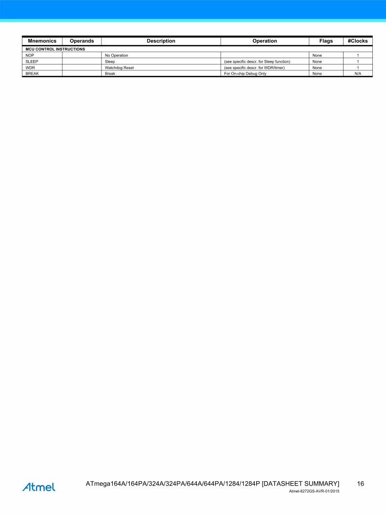
MCU CONTROL INSTRUCTIONS
NOP No Operation None 1
SLEEP Sleep (see specific descr. for Sleep function) None 1
WDR Watchdog Reset (see specific descr. for WDR/timer) None 1
BREAK Break For On-chip Debug Only None N/A
Mnemonics Operands Description Operation Flags #Clocks
16ATmega164A/164PA/324A/324PA/644A/644PA/1284/1284P [DATASHEET SUMMARY]Atmel-8272GS-AVR-01/2015
9. Ordering information
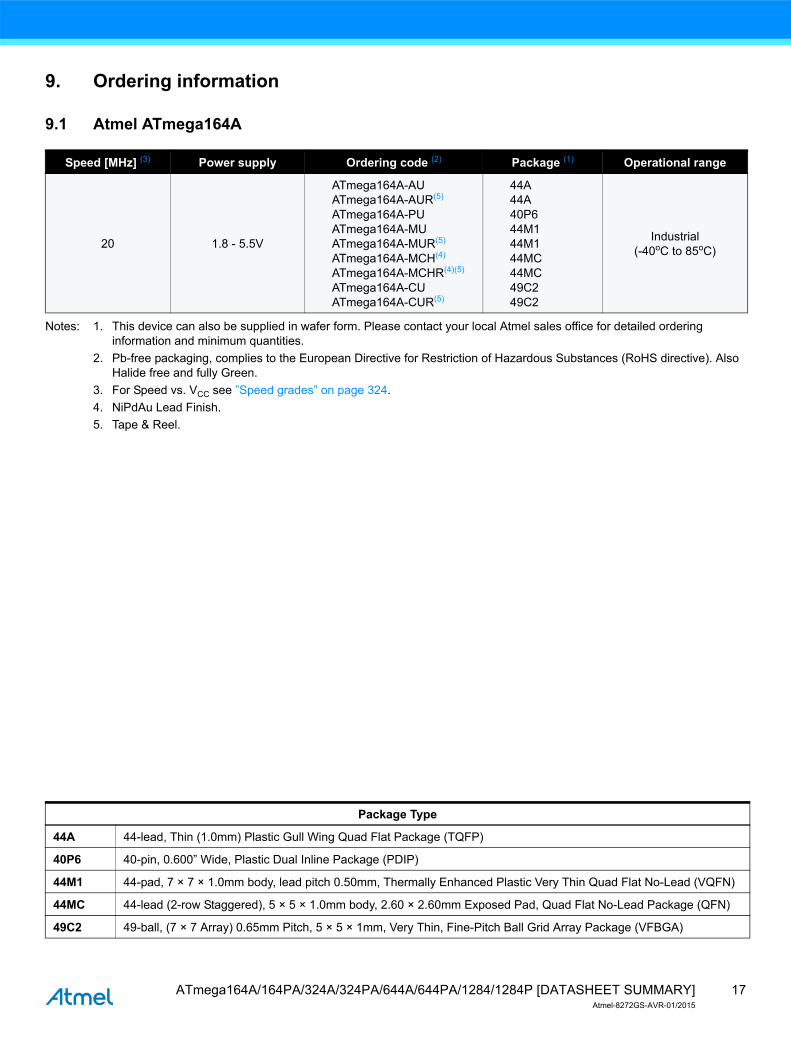
9.1 Atmel ATmega164A
Notes: 1. This device can also be supplied in wafer form. Please contact your local Atmel sales office for detailed ordering information and minimum quantities.
2. Pb-free packaging, complies to the European Directive for Restriction of Hazardous Substances (RoHS directive). Also Halide free and fully Green.
3. For Speed vs. VCC see ”Speed grades” on page 324.
4. NiPdAu Lead Finish.
5. Tape & Reel.
Speed [MHz] (3) Power supply Ordering code (2) Package (1) Operational range
20 1.8 - 5.5V
ATmega164A-AUATmega164A-AUR(5)
ATmega164A-PUATmega164A-MUATmega164A-MUR(5)
ATmega164A-MCH(4)
ATmega164A-MCHR(4)(5)
ATmega164A-CUATmega164A-CUR(5)
44A44A40P644M144M144MC44MC49C249C2
Industrial(-40oC to 85oC)
Package Type
44A 44-lead, Thin (1.0mm) Plastic Gull Wing Quad Flat Package (TQFP)
40P6 40-pin, 0.600” Wide, Plastic Dual Inline Package (PDIP)
44M1 44-pad, 7 × 7 × 1.0mm body, lead pitch 0.50mm, Thermally Enhanced Plastic Very Thin Quad Flat No-Lead (VQFN)
44MC 44-lead (2-row Staggered), 5 × 5 × 1.0mm body, 2.60 × 2.60mm Exposed Pad, Quad Flat No-Lead Package (QFN)
49C2 49-ball, (7 × 7 Array) 0.65mm Pitch, 5 × 5 × 1mm, Very Thin, Fine-Pitch Ball Grid Array Package (VFBGA)
17ATmega164A/164PA/324A/324PA/644A/644PA/1284/1284P [DATASHEET SUMMARY]Atmel-8272GS-AVR-01/2015
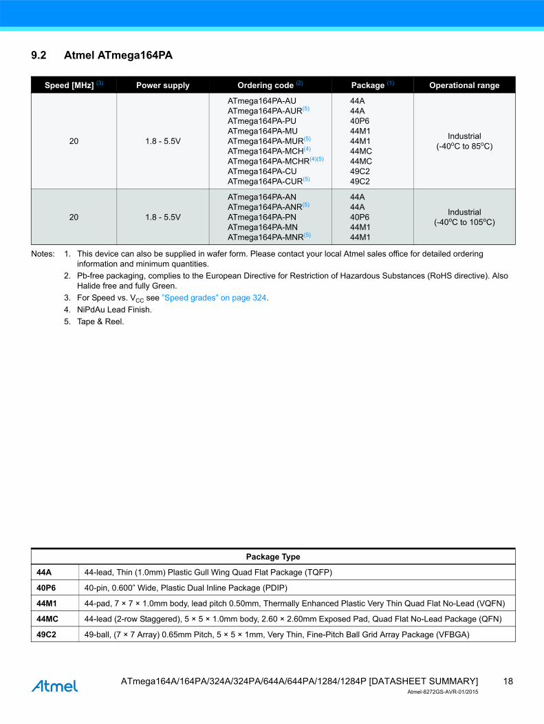
9.2 Atmel ATmega164PA
Notes: 1. This device can also be supplied in wafer form. Please contact your local Atmel sales office for detailed ordering information and minimum quantities.
2. Pb-free packaging, complies to the European Directive for Restriction of Hazardous Substances (RoHS directive). Also Halide free and fully Green.
3. For Speed vs. VCC see ”Speed grades” on page 324.
4. NiPdAu Lead Finish.
5. Tape & Reel.
Speed [MHz] (3) Power supply Ordering code (2) Package (1) Operational range
20 1.8 - 5.5V
ATmega164PA-AUATmega164PA-AUR(5)
ATmega164PA-PUATmega164PA-MUATmega164PA-MUR(5)
ATmega164PA-MCH(4)
ATmega164PA-MCHR(4)(5)
ATmega164PA-CUATmega164PA-CUR(5)
44A44A40P644M144M144MC44MC49C249C2
Industrial(-40oC to 85oC)
20 1.8 - 5.5V
ATmega164PA-ANATmega164PA-ANR(5)
ATmega164PA-PNATmega164PA-MNATmega164PA-MNR(5)
44A44A40P644M144M1
Industrial(-40oC to 105oC)
Package Type
44A 44-lead, Thin (1.0mm) Plastic Gull Wing Quad Flat Package (TQFP)
40P6 40-pin, 0.600” Wide, Plastic Dual Inline Package (PDIP)
44M1 44-pad, 7 × 7 × 1.0mm body, lead pitch 0.50mm, Thermally Enhanced Plastic Very Thin Quad Flat No-Lead (VQFN)
44MC 44-lead (2-row Staggered), 5 × 5 × 1.0mm body, 2.60 × 2.60mm Exposed Pad, Quad Flat No-Lead Package (QFN)
49C2 49-ball, (7 × 7 Array) 0.65mm Pitch, 5 × 5 × 1mm, Very Thin, Fine-Pitch Ball Grid Array Package (VFBGA)
18ATmega164A/164PA/324A/324PA/644A/644PA/1284/1284P [DATASHEET SUMMARY]Atmel-8272GS-AVR-01/2015
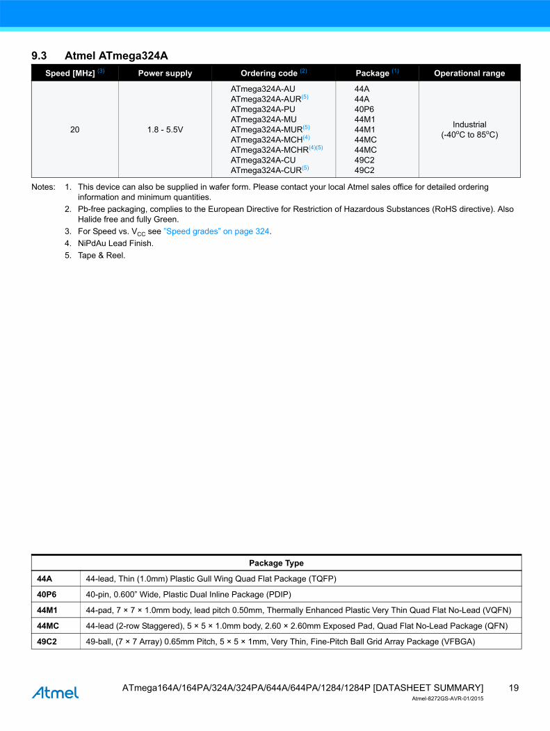
9.3 Atmel ATmega324A
Notes: 1. This device can also be supplied in wafer form. Please contact your local Atmel sales office for detailed ordering information and minimum quantities.
2. Pb-free packaging, complies to the European Directive for Restriction of Hazardous Substances (RoHS directive). Also Halide free and fully Green.
3. For Speed vs. VCC see ”Speed grades” on page 324.
4. NiPdAu Lead Finish.
5. Tape & Reel.
Speed [MHz] (3) Power supply Ordering code (2) Package (1) Operational range
20 1.8 - 5.5V
ATmega324A-AUATmega324A-AUR(5)
ATmega324A-PUATmega324A-MUATmega324A-MUR(5)
ATmega324A-MCH(4)
ATmega324A-MCHR(4)(5)
ATmega324A-CUATmega324A-CUR(5)
44A44A40P644M144M144MC44MC49C249C2
Industrial(-40oC to 85oC)
Package Type
44A 44-lead, Thin (1.0mm) Plastic Gull Wing Quad Flat Package (TQFP)
40P6 40-pin, 0.600” Wide, Plastic Dual Inline Package (PDIP)
44M1 44-pad, 7 × 7 × 1.0mm body, lead pitch 0.50mm, Thermally Enhanced Plastic Very Thin Quad Flat No-Lead (VQFN)
44MC 44-lead (2-row Staggered), 5 × 5 × 1.0mm body, 2.60 × 2.60mm Exposed Pad, Quad Flat No-Lead Package (QFN)
49C2 49-ball, (7 × 7 Array) 0.65mm Pitch, 5 × 5 × 1mm, Very Thin, Fine-Pitch Ball Grid Array Package (VFBGA)
19ATmega164A/164PA/324A/324PA/644A/644PA/1284/1284P [DATASHEET SUMMARY]Atmel-8272GS-AVR-01/2015

9.4 Atmel ATmega324PA
Notes: 1. This device can also be supplied in wafer form. Please contact your local Atmel sales office for detailed ordering information and minimum quantities.
2. Pb-free packaging, complies to the European Directive for Restriction of Hazardous Substances (RoHS directive). Also Halide free and fully Green.
3. For Speed vs. VCC see ”Speed grades” on page 324.
4. NiPdAu Lead Finish.
5. Tape & Reel.
Speed [MHz] (3) Power supply Ordering code (2) Package (1) Operational range
20 1.8 - 5.5V
ATmega324PA-AUATmega324PA-AUR(5)
ATmega324PA-PUATmega324PA-MUATmega324PA-MUR(5)
ATmega324PA-MCH(4)
ATmega324PA-MCHR(4)(5)
ATmega324PA-CUATmega324PA-CUR(5)
44A44A40P644M144M144MC44MC49C249C2
Industrial(-40oC to 85oC)
20 1.8 - 5.5V
ATmega324PA-ANATmega324PA-ANR(5)
ATmega324PA-PNATmega324PA-MNATmega324PA-MNR(5)
44A44A40P644M144M1
Industrial(-40oC to 105oC)
Package Type
44A 44-lead, Thin (1.0mm) Plastic Gull Wing Quad Flat Package (TQFP)
40P6 40-pin, 0.600” Wide, Plastic Dual Inline Package (PDIP)
44M1 44-pad, 7 × 7 × 1.0mm body, lead pitch 0.50mm, Thermally Enhanced Plastic Very Thin Quad Flat No-Lead (VQFN)
44MC 44-lead (2-row Staggered), 5 × 5 × 1.0mm body, 2.60 × 2.60mm Exposed Pad, Quad Flat No-Lead Package (QFN)
49C2 49-ball, (7 × 7 Array) 0.65mm Pitch, 5 × 5 × 1mm, Very Thin, Fine-Pitch Ball Grid Array Package (VFBGA)
20ATmega164A/164PA/324A/324PA/644A/644PA/1284/1284P [DATASHEET SUMMARY]Atmel-8272GS-AVR-01/2015

9.5 Atmel ATmega644A
Notes: 1. This device can also be supplied in wafer form. Please contact your local Atmel sales office for detailed ordering information and minimum quantities.
2. Pb-free packaging, complies to the European Directive for Restriction of Hazardous Substances (RoHS directive). Also Halide free and fully Green.
3. For Speed vs. VCC see ”Speed grades” on page 324.
4. Taper & Reel.
Speed [MHz](3) Power supply Ordering code(2) Package(1) Operational range
20 1.8 - 5.5V
ATmega644A-AUATmega644A-AUR(4)
ATmega644A-PUATmega644A-MUATmega644A-MUR(4)
44A44A40P644M144M1
Industrial(-40oC to 85oC)
Package Type
44A 44-lead, Thin (1.0mm) Plastic Gull Wing Quad Flat Package (TQFP)
40P6 40-pin, 0.600” Wide, Plastic Dual Inline Package (PDIP)
44M1 44-pad, 7 × 7 × 1.0mm body, lead pitch 0.5 mm, Thermally Enhanced Plastic Very Thin Quad Flat No-Lead (VQFN)
21ATmega164A/164PA/324A/324PA/644A/644PA/1284/1284P [DATASHEET SUMMARY]Atmel-8272GS-AVR-01/2015
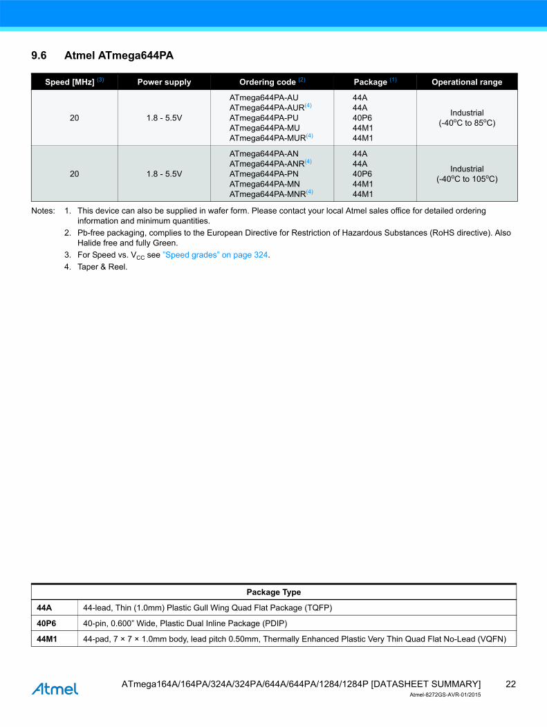
9.6 Atmel ATmega644PA
Notes: 1. This device can also be supplied in wafer form. Please contact your local Atmel sales office for detailed ordering information and minimum quantities.
2. Pb-free packaging, complies to the European Directive for Restriction of Hazardous Substances (RoHS directive). Also Halide free and fully Green.
3. For Speed vs. VCC see ”Speed grades” on page 324.
4. Taper & Reel.
Speed [MHz] (3) Power supply Ordering code (2) Package (1) Operational range
20 1.8 - 5.5V
ATmega644PA-AUATmega644PA-AUR(4)
ATmega644PA-PUATmega644PA-MUATmega644PA-MUR(4)
44A44A40P644M144M1
Industrial(-40oC to 85oC)
20 1.8 - 5.5V
ATmega644PA-ANATmega644PA-ANR(4)
ATmega644PA-PNATmega644PA-MNATmega644PA-MNR(4)
44A44A40P644M144M1
Industrial(-40oC to 105oC)
Package Type
44A 44-lead, Thin (1.0mm) Plastic Gull Wing Quad Flat Package (TQFP)
40P6 40-pin, 0.600” Wide, Plastic Dual Inline Package (PDIP)
44M1 44-pad, 7 × 7 × 1.0mm body, lead pitch 0.50mm, Thermally Enhanced Plastic Very Thin Quad Flat No-Lead (VQFN)
22ATmega164A/164PA/324A/324PA/644A/644PA/1284/1284P [DATASHEET SUMMARY]Atmel-8272GS-AVR-01/2015
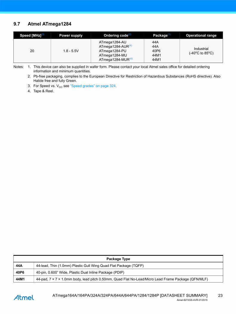
9.7 Atmel ATmega1284
Notes: 1. This device can also be supplied in wafer form. Please contact your local Atmel sales office for detailed ordering information and minimum quantities.
2. Pb-free packaging, complies to the European Directive for Restriction of Hazardous Substances (RoHS directive). Also Halide free and fully Green.
3. For Speed vs. VCC see ”Speed grades” on page 324.
4. Tape & Reel.
Speed [MHz](3) Power supply Ordering code(2) Package(1) Operational range
20 1.8 - 5.5V
ATmega1284-AUATmega1284-AUR(4)
ATmega1284-PUATmega1284-MUATmega1284-MUR(4)
44A44A40P644M144M1
Industrial(-40oC to 85oC)
Package Type
44A 44-lead, Thin (1.0mm) Plastic Gull Wing Quad Flat Package (TQFP)
40P6 40-pin, 0.600” Wide, Plastic Dual Inline Package (PDIP)
44M1 44-pad, 7 × 7 × 1.0mm body, lead pitch 0.50mm, Quad Flat No-Lead/Micro Lead Frame Package (QFN/MLF)
23ATmega164A/164PA/324A/324PA/644A/644PA/1284/1284P [DATASHEET SUMMARY]Atmel-8272GS-AVR-01/2015

9.8 Atmel ATmega1284P
Notes: 1. This device can also be supplied in wafer form. Please contact your local Atmel sales office for detailed ordering information and minimum quantities.
2. Pb-free packaging, complies to the European Directive for Restriction of Hazardous Substances (RoHS directive). Also Halide free and fully Green.
3. For Speed vs. VCC see ”Speed grades” on page 324.
4. Tape & Reel.
Speed [MHz] (3) Power supply Ordering code (2) Package (1) Operational range
20 1.8 - 5.5V
ATmega1284P-AUATmega1284P-AUR(4)
ATmega1284P-PUATmega1284P-MUATmega1284P-MUR(4)
44A44A40P644M144M1
Industrial(-40oC to 85oC)
20 1.8 - 5.5V
ATmega1284P-ANATmega1284P-ANR(4)
ATmega1284P-PNATmega1284P-MNATmega1284P-MNR(4)
44A44A40P644M144M1
Industrial(-40oC to 105oC)
Package Type
44A 44-lead, Thin (1.0mm) Plastic Gull Wing Quad Flat Package (TQFP)
40P6 40-pin, 0.600” Wide, Plastic Dual Inline Package (PDIP)
44M1 44-pad, 7 × 7 × 1.0mm body, lead pitch 0.50mm, Quad Flat No-Lead/Micro Lead Frame Package (QFN/MLF)
24ATmega164A/164PA/324A/324PA/644A/644PA/1284/1284P [DATASHEET SUMMARY]Atmel-8272GS-AVR-01/2015
10. Packaging information
10.1 44A
44A, 44-lead, 10 x 10mm body size, 1.0mm body thickness,0.8 mm lead pitch, thin profile plastic quad flat package (TQFP)
C44A
06/02/2014
PIN 1 IDENTIFIER
0°~7°
PIN 1
L
C
A1 A2 A
D1
D
e
E1 E
B
COMMON DIMENSIONS(Unit of Measure = mm)
SYMBOL MIN NOM MAX NOTE
Notes: 1. This package conforms to JEDEC reference MS-026, Variation ACB. 2. Dimensions D1 and E1 do not include mold protrusion. Allowable protrusion is 0.25mm per side. Dimensions D1 and E1 are maximum plastic body size dimensions including mold mismatch. 3. Lead coplanarity is 0.10mm maximum.
A – – 1.20
A1 0.05 – 0.15
A2 0.95 1.00 1.05
D 11.75 12.00 12.25
D1 9.90 10.00 10.10 Note 2
E 11.75 12.00 12.25
E1 9.90 10.00 10.10 Note 2
B 0.30 0.37 0.45
C 0.09 (0.17) 0.20
L 0.45 0.60 0.75
e 0.80 TYP
25ATmega164A/164PA/324A/324PA/644A/644PA/1284/1284P [DATASHEET SUMMARY]Atmel-8272GS-AVR-01/2015
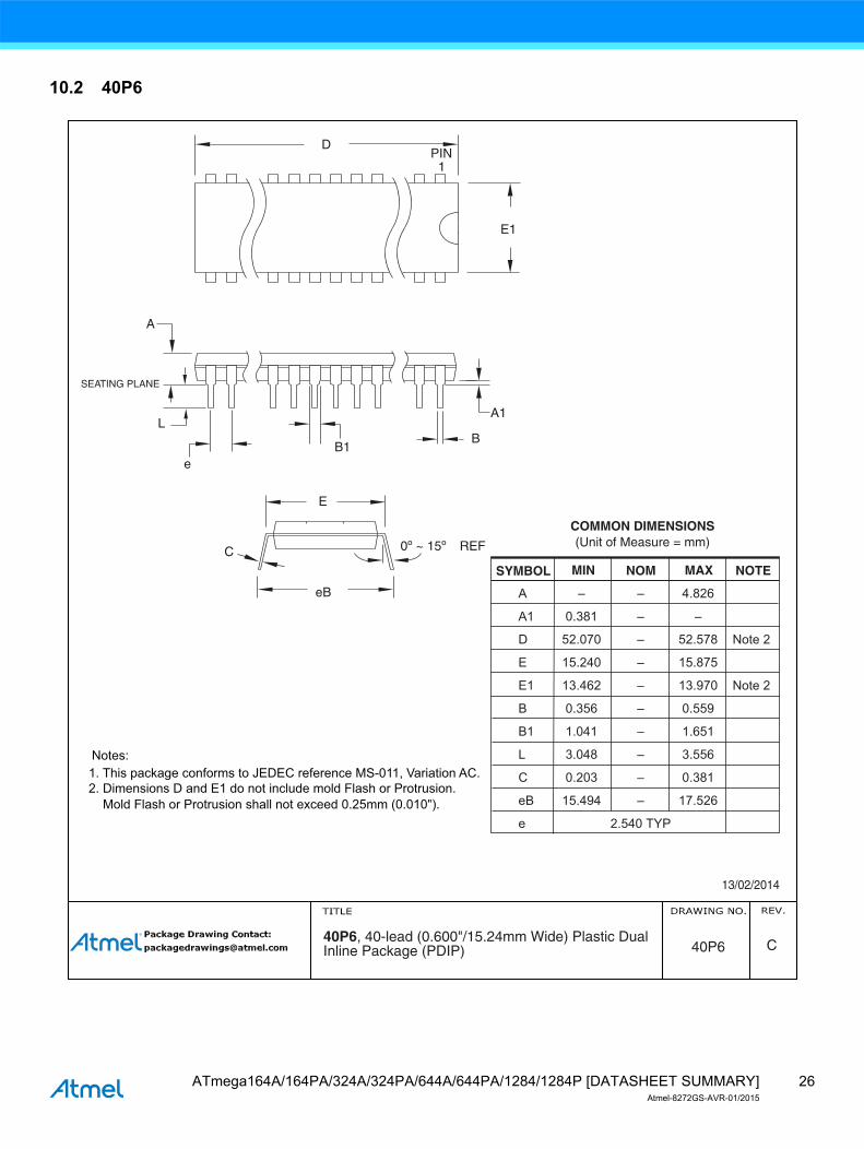
10.2 40P6
PIN1
E1
A1
B
REF
E
B1
C
L
SEATING PLANE
A
0º ~ 15º
D
e
eB
COMMON DIMENSIONS(Unit of Measure = mm)
SYMBOL MIN NOM MAX NOTE
A – – 4.826
A1 0.381 – –
D 52.070 – 52.578 Note 2
E 15.240 – 15.875
E1 13.462 – 13.970 Note 2
B 0.356 – 0.559
B1 1.041 – 1.651
L 3.048 – 3.556
C 0.203 – 0.381
eB 15.494 – 17.526
e 2.540 TYP
1. This package conforms to JEDEC reference MS-011, Variation AC.2. Dimensions D and E1 do not include mold Flash or Protrusion. Mold Flash or Protrusion shall not exceed 0.25mm (0.010").
Notes:
40P6, 40-lead (0.600"/15.24mm Wide) Plastic Dual Inline Package (PDIP) 40P6 C
13/02/2014
26ATmega164A/164PA/324A/324PA/644A/644PA/1284/1284P [DATASHEET SUMMARY]Atmel-8272GS-AVR-01/2015

10.3 44M1
TITLE DRAWING NO.GPC REV. Package Drawing Contact: [email protected] 44M1ZWS H
44M1, 44-pad, 7 x 7 x 1.0mm body, lead pitch 0.50mm, 5.20mm exposed pad, thermally enhanced plastic very thin quad flat no lead package (VQFN)
9/26/08
COMMON DIMENSIONS(Unit of Measure = mm)
SYMBOL MIN NOM MAX NOT E
A 0.80 0.90 1.00
A1 – 0.02 0.05
A3 0.20 REF
b 0.18 0.23 0.30
D
D2 5.00 5.20 5.40
6.90 7.00 7.10
6.90 7.00 7.10
E
E2 5.00 5.20 5.40
e 0.50 BSC
L 0.59 0.64 0.69
K 0.20 0.26 0.41Note: JEDEC Standard MO-220, Fig . 1 (S AW Singulation) VKKD-3 .
TOP VIE W
SIDE VIEW
B OT TOM VIE W
D
E
Marked Pin# 1 I D
E2
D2
b e
Pin #1 Co rnerL
A1
A3
A
SE ATING PLAN E
Pin #1 Triangle
Pin #1 Cham fer(C 0.30)
Option A
Option B
Pin #1 Notch(0.20 R)
Option C
K
K
123
27ATmega164A/164PA/324A/324PA/644A/644PA/1284/1284P [DATASHEET SUMMARY]Atmel-8272GS-AVR-01/2015

10.4 44MC
TITLE DRA WING NO . REV . Package Drawing Contact: [email protected] 44MC A
9/13/07
D2
E2L L
B15
A18
B11
A13
B10
A12
B6
A7
A6
B5
B1
B20
A1
A24
eT
L
b
R0.20 0.40
eR
A19
B16
eT/2
SIDE VIEW
A1A
y
C
D
E
Pin 1 ID
TOP VIEW
BOTTOM VIEW
Note: 1. The terminal #1 ID is a Laser-marked Feature.
COMMON DIMENSIONS(Unit of Measure = mm)
SYMBOL MIN NOM MAX NOT E
A 0.80 0.90 1.00
A1 0.00 0.02 0.05
b 0.18 0.23 0.30
C 0.20 REF
D 4.90 5.00 5.10
D2 2.55 2.60 2.65
E 4.90 5.00 5.10
E2 2.55 2.60 2.65
eT – 0.70 –
eR – 0.40 –
K 0.45 – –
L 0.30 0.35 0.40
y 0.00 – 0.075
44MC, 44QFN (2-Row Staggered), 5 x 5 x 1.00 mm Body, 2.60 x 2.60 mm Exposed Pad, Quad Flat No Lead Package
28ATmega164A/164PA/324A/324PA/644A/644PA/1284/1284P [DATASHEET SUMMARY]Atmel-8272GS-AVR-01/2015
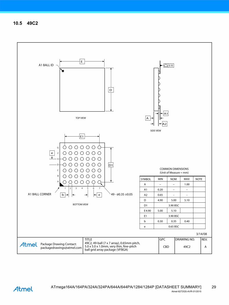
10.5 49C2
TITLE DRAWING NO.GPC REV. Package Drawing Contact: [email protected] 49C2CBD A
49C2, 49-ball (7 x 7 array), 0.65mm pitch, 5.0 x 5.0 x 1.0mm, very thin, fine-pitch ball grid array package (VFBGA)
3/14/08
COMMON DIMENSIONS(Unit of Measure = mm)
SYMBOL MIN NOM MAX NOTE
A – – 1.00
A1 0.20 – –
A2 0.65 – –
D 4.90 5.00 5.10
D1 3.90 BSC
E 4.90 5.00 5.10
E1 3.90 BSC
b 0.30 0.35 0.40
e 0.65 BSC
TOP VIEW
SIDE VIEW
A1 BALL ID
G
F
E
D
C
B
A
1 2 3 4 5 6 7
A
A1
A2
D
E0.10
E1
D1
49 - Ø0.35 ±0.05
e
A1 BALL CORNER
BOTTOM VIEW
b e
29ATmega164A/164PA/324A/324PA/644A/644PA/1284/1284P [DATASHEET SUMMARY]Atmel-8272GS-AVR-01/2015
11. Errata
11.1 Errata for ATmega164A
11.1.1 Rev. E
No known Errata.
11.2 Errata for ATmega164PA
11.2.1 Rev. E
No known Errata.
11.3 Errata for ATmega324A
11.3.1 Rev. F
No known Errata.
11.4 Errata for ATmega324PA
11.4.1 Rev. F
No known Errata.
11.5 Errata for ATmega644A
11.5.1 Rev. F
No known Errata.
11.6 Errata for ATmega644PA
11.6.1 Rev. F
No known Errata.
11.7 Errata for ATmega1284
11.7.1 Rev. B
No known Errata.
11.8 Errata for ATmega1284P
11.8.1 Rev. B
No known Errata.
30ATmega164A/164PA/324A/324PA/644A/644PA/1284/1284P [DATASHEET SUMMARY]Atmel-8272GS-AVR-01/2015

12. Datasheet revision history
Please note that the referring page numbers in this section are referred to this document. The referring revision in this section are referring to the document revision.
12.1 Rev. 8272G - 01/2015
12.2 Rev. 8272F - 08/2014
1.Updated Table 1-2 on page 5, Table 8-1 on page 25, Table 10-1 on page 42, Table 14-3 on page 79, Table 19-4 on page 187, Table 19-11 on page 192 and Table 28-16 on page 328 for formatting consistency errors
2.
Updated ”Ordering information” on page 17:
Added ordering information for ATmega164PA @105C; ATmega324PA @ 105C; ATmega324PA
@105C; ATmega644PA @ 105C and ATmega1284P @ 105C
3.Updated the ”Packaging information” on page 25:
Replaced the drawing ”44M1” on page 27 by a correct package
1.Updated text in Section 13.2.8 ”PCMSK1 – Pin Change Mask Register 1” on page 70 to: “If PCINT15:8 is set and the PCIE1 bit in PCICR is set, pin change interrupt is enabled on the corresponding I/O pin.”
2. Corrected description of PAGEMSB in Table 26-9 on page 281. The device has 64 words in a page and not 128.
3.Corrected description of PAGEMSB in Table 26-12 on page 282. PAGESMB is 5 and the device has 64 words in a page and not 128. The page require six bits and not seven.
4. Corrected values in Table 26-16 on page 284. PAGEMSB is 6. ZPAGEMSB is Z7 and PCPAGE is Z15:Z8
5. Corrected value for PCPAGE in Table 27-7 on page 290. The correct value is PC[14:7]
6. Updated description in Table 17-2 on page 151 to “Normal port operation, OC2A disconnected.”
7.
Updated Assembly code examples on for ”Watchdog Timer” on page 55. and onwards“out WDTCSR, r16” changed to “sts WDTCSR, r16”“in r16, WDTCSR” changed to “lds r16, WDTCSR”“idi r16, WDTCSR” changed to “lds r16, WDTCSR”
8. Updated addresses 0x65 and 0x64 in Section 7. ”Register summary” on page 10.
9. Removed notes 5 and 6 from Table 28-16 on page 328.
10.Corrected values in Section 8. ”Instruction set summary” on page 14.Changed clock values for RCALL and ICALL to 2, for Call, Ret and RETI to 4. Also changed values in Section 7.7.1 ”Interrupt response time” on page 18.
11. Updated layout, footer and back page according to template 0205/2014
31ATmega164A/164PA/324A/324PA/644A/644PA/1284/1284P [DATASHEET SUMMARY]Atmel-8272GS-AVR-01/2015
12.3 Rev. 8272E - 04/2013
12.4 Rev. 8272D - 05/12
12.5 Rev. 8272C - 06/11
12.6 Rev. 8272B - 05/11
1. Updated Figure 1-1 on page 3 and Figure 2-1 on page 6: T3 and T/C3 only available in ATmega1284/1284P.
2. Updated descriptive text on page 6 to indicate that ATmega1284/1284P has four T/Cs.3. Updated the Assembly code example for WDT_off (p.56) following the ej# 705736.
4. Added note in ”16-bit Timer/Counter1 and Timer/Counter3(1) with PWM” on page 107.
5. Added ”Prescaler Reset” on page 112.
6. Corrected three typo for Waveform generation mode (WGM) instead of MGM.
7.Updated Table 23-6 on page 253. ADC Auto Trigger Source Selections, ADTS=0b011, the statement is Timer/Counter0 Compare Match A.
8. Updated Table 27-18 on page 310. Command for 6d Poll for Fuse Write Complete: 0111011_00000000
9. Updated the table notes of the Table 28-1 on page 318.
10. Updated ”Register summary” on page 10. Added table note 7: Only available in ATmega1284/1284P.
1. Updated ”Power-down mode” on page 44.
2. Updated ”Overview” on page 67.
3.Corrected references for Bit 2, Bit 1, and Bit 0 in Section ”UCSRnC – USART MSPIM Control and Status Register n C” on page 201.
4. Several small corrections throughout the whole document made according to the template
5. Notes in Table 27-17 on page 304 have been corrected
6. Note (1) in Table 28-3 on page 320 is added
1. Updated ”Atmel ATmega1284P DC characteristics” on page 323.
1. Added Atmel QTouch Library Support and QTouch Sensing Capability Features.
2. Replaced the Figure 1-1 on page 3 by an updated “Pinout.” that includes Timer/Counter3.
3.Replaced the Figure 7-1 on page 10 by an updated “Block diagram of the AVR architecture.” that includes Timer/Counter3.
4. Added ”RAMPZ – Extended Z-pointer Register for ELPM/SPM(1)” on page 15.
5. Added ”PRR1 – Power Reduction Register 1” on page 49.
6. Renamed PRR to ”PRR0 – Power Reduction Register 0” on page 48.
7. Updated ”PCIFR – Pin Change Interrupt Flag Register” on page 69. PCICR replaces EIMSR in the PCIF3, PCIF2, PCIF1 and PCIF0 bit description.
8. Updated ”PCMSK3 – Pin Change Mask Register 3” on page 70. PCIE3 replaces PCIE2 in the bit description.
9. Updated ”Alternate Functions of Port B” on page 80 to include Timer/Counter3
10. Updated ”Alternate Functions of Port D” on page 86 to include Timer/Counter3
11. Added ”TCNT3H and TCNT3L –Timer/Counter3” on page 132
32ATmega164A/164PA/324A/324PA/644A/644PA/1284/1284P [DATASHEET SUMMARY]Atmel-8272GS-AVR-01/2015
12.7 Rev. 8272A - 01/10
12. Added ”OCR3AH and OCR3AL – Output Compare Register3 A” on page 133
13. Added ”OCR3BH and OCR3BL – Output Compare Register3 B” on page 133
14. Added ”TIMSK3 – Timer/Counter3 Interrupt Mask Register” on page 134
15. Updated All “SPI – Serial Peripheral Interface” “Register description” to reflect ATmega1284 and ATmega1284P.
16. Updated ”Addressing the Flash During Self-Programming” on page 274 to include RAMPZ register.
17. Updated Table 27-16 on page 303. tWD_EEPROM is 3.6ms instead of 9ms.
18. BODS and BODSE bits denoted as R/W
19. Description of external pin modes below table 16-9 removed.
20. Updated ”Register summary” on page 10 to include Timer/Counter3.
21. Updated the datasheet with Atmel new style guide.
1. Initial revision (Based on the ATmega164PA/324PA/644PA/1284P datasheet 8252G-AVR-11/09 and on the ATmega644 datasheet 2593N-AVR-09/09).
2. Changes done:
Non-picoPower devices added: ATmega164A/324A/644A/1284
Updated Table 2-1 on page 7
Updated Table 10-1 on page 42
Updated ”Sleep Modes” on page 42 and ”BOD disable(1)” on page 43
Updated ”Register description” on page 67
Updated ”USART” on page 167 and ”USART in SPI mode” on page 194
Updated ”Signature Bytes” on page 290 and ”Page Size” on page 290
Added ”DC Characteristics” on page 318 for non-picoPower devices.
Added ”Atmel ATmega164A typical characteristics” on page 333
Added ”Atmel ATmega324A typical characteristics” on page 386
Added ”Atmel ATmega644A typical characteristics” on page 438
Added ”ATmega1284 typical characteristics” on page 490
Added ”Ordering information” on page 17 for non-picoPower devices
Added ”Errata for ATmega164A” on page 30
Added ”Errata for ATmega324A” on page 30
Added ”Errata for ATmega644PA” on page 30
Added ”Errata for ATmega1284” on page 30
33ATmega164A/164PA/324A/324PA/644A/644PA/1284/1284P [DATASHEET SUMMARY]Atmel-8272GS-AVR-01/2015


XX X XX X
Atmel Corporation 1600 Technology Drive, San Jose, CA 95110 USA T: (+1)(408) 441.0311 F: (+1)(408) 436.4200 | www.atmel.com
© 2015 Atmel Corporation. / Rev.: Atmel-8272GS-AVR-ATmega164A/PA/324A/PA/644A/PA/1284/P-Datasheet Summary_01/2015.
Atmel®, Atmel logo and combinations thereof, Enabling Unlimited Possibilities, and others are registered trademarks or trademarks of Atmel Corporation in U.S. and other countries. Other terms and product names may be trademarks of others.
DISCLAIMER: The information in this document is provided in connection with Atmel products. No license, express or implied, by estoppel or otherwise, to any intellectual property rightis granted by this document or in connection with the sale of Atmel products. EXCEPT AS SET FORTH IN THE ATMEL TERMS AND CONDITIONS OF SALES LOCATED ON THEATMEL WEBSITE, ATMEL ASSUMES NO LIABILITY WHATSOEVER AND DISCLAIMS ANY EXPRESS, IMPLIED OR STATUTORY WARRANTY RELATING TO ITS PRODUCTSINCLUDING, BUT NOT LIMITED TO, THE IMPLIED WARRANTY OF MERCHANTABILITY, FITNESS FOR A PARTICULAR PURPOSE, OR NON-INFRINGEMENT. IN NO EVENTSHALL ATMEL BE LIABLE FOR ANY DIRECT, INDIRECT, CONSEQUENTIAL, PUNITIVE, SPECIAL OR INCIDENTAL DAMAGES (INCLUDING, WITHOUT LIMITATION, DAMAGESFOR LOSS AND PROFITS, BUSINESS INTERRUPTION, OR LOSS OF INFORMATION) ARISING OUT OF THE USE OR INABILITY TO USE THIS DOCUMENT, EVEN IF ATMEL HASBEEN ADVISED OF THE POSSIBILITY OF SUCH DAMAGES. Atmel makes no representations or warranties with respect to the accuracy or completeness of the contents of thisdocument and reserves the right to make changes to specifications and products descriptions at any time without notice. Atmel does not make any commitment to update the informationcontained herein. Unless specifically provided otherwise, Atmel products are not suitable for, and shall not be used in, automotive applications. Atmel products are not intended,authorized, or warranted for use as components in applications intended to support or sustain life.
SAFETY-CRITICAL, MILITARY, AND AUTOMOTIVE APPLICATIONS DISCLAIMER: Atmel products are not designed for and will not be used in connection with any applications wherethe failure of such products would reasonably be expected to result in significant personal injury or death (“Safety-Critical Applications”) without an Atmel officer's specific writtenconsent. Safety-Critical Applications include, without limitation, life support devices and systems, equipment or systems for the operation of nuclear facilities and weapons systems.Atmel products are not designed nor intended for use in military or aerospace applications or environments unless specifically designated by Atmel as military-grade. Atmel products are
not designed nor intended for use in automotive applications unless specifically designated by Atmel as automotive-grade.