8-channel multiplexer - home - s · pdf filem74hc151 8-channel multiplexer datasheet -...
TRANSCRIPT
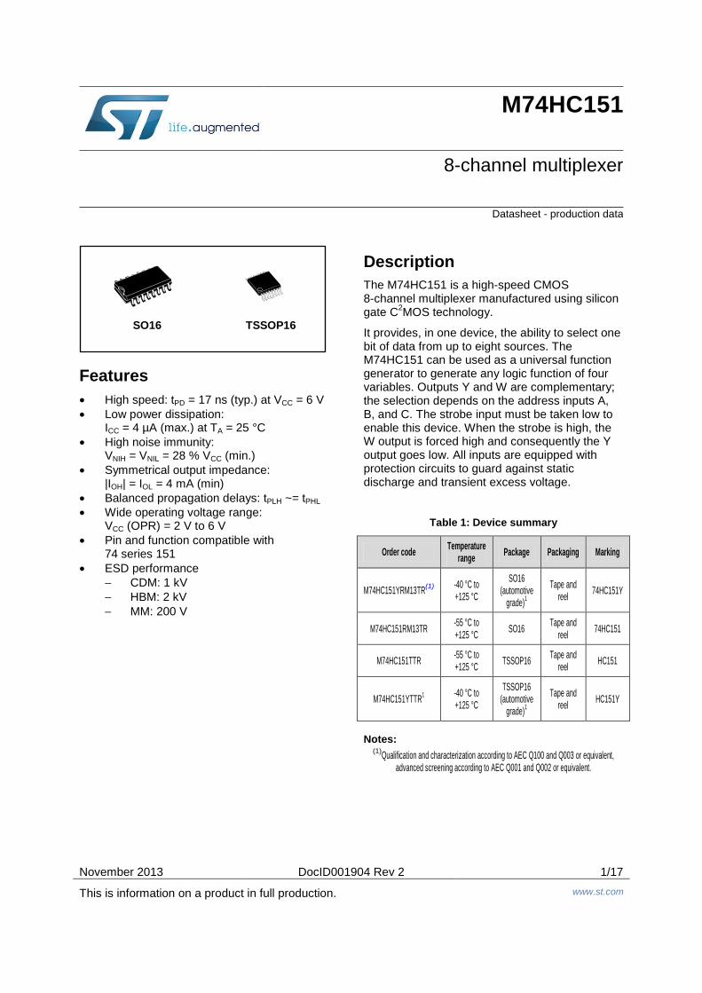
M74HC151
8-channel multiplexer
Datasheet - production data
Features • High speed: tPD = 17 ns (typ.) at VCC = 6 V • Low power dissipation:
ICC = 4 µA (max.) at TA = 25 °C • High noise immunity:
VNIH = VNIL = 28 % VCC (min.) • Symmetrical output impedance:
|IOH| = IOL = 4 mA (min) • Balanced propagation delays: tPLH ~= tPHL • Wide operating voltage range:
VCC (OPR) = 2 V to 6 V • Pin and function compatible with
74 series 151 • ESD performance
− CDM: 1 kV − HBM: 2 kV − MM: 200 V
Description The M74HC151 is a high-speed CMOS 8-channel multiplexer manufactured using silicon gate C2MOS technology.
It provides, in one device, the ability to select one bit of data from up to eight sources. The M74HC151 can be used as a universal function generator to generate any logic function of four variables. Outputs Y and W are complementary; the selection depends on the address inputs A, B, and C. The strobe input must be taken low to enable this device. When the strobe is high, the W output is forced high and consequently the Y output goes low. All inputs are equipped with protection circuits to guard against static discharge and transient excess voltage.
Table 1: Device summary
Order code Temperature range Package Packaging Marking
M74HC151YRM13TR(1) -40 °C to +125 °C
SO16 (automotive
grade)1
Tape and reel 74HC151Y
M74HC151RM13TR -55 °C to +125 °C SO16 Tape and
reel 74HC151
M74HC151TTR -55 °C to +125 °C TSSOP16 Tape and
reel HC151
M74HC151YTTR1 -40 °C to +125 °C
TSSOP16 (automotive
grade)1
Tape and reel HC151Y
Notes: (1)Qualification and characterization according to AEC Q100 and Q003 or equivalent,
advanced screening according to AEC Q001 and Q002 or equivalent.
TSSOP16SO16
November 2013 DocID001904 Rev 2 1/17
This is information on a product in full production. www.st.com
Contents M74HC151
Contents 1 Pin information ................................................................................ 5
2 Functional description .................................................................... 6
3 Electrical characteristics ................................................................ 8
4 Package information ..................................................................... 13
4.1 SO16 package information .............................................................. 13
4.2 TSSOP16 package information ....................................................... 15
5 Revision history ............................................................................ 16
2/17 DocID001904 Rev 2
M74HC151 List of tables
List of tables Table 1: Device summary ........................................................................................................................... 1 Table 2: Pin description .............................................................................................................................. 5 Table 3: Truth table ..................................................................................................................................... 6 Table 4: Absolute maximum ratings ........................................................................................................... 8 Table 5: Recommended operating conditions ............................................................................................ 8 Table 6: DC specifications .......................................................................................................................... 9 Table 7: AC electrical characteristics (CL = 50 pF, input tr = tf = 6 ns) ..................................................... 10 Table 8: Capacitive characteristics ........................................................................................................... 11 Table 9: Plastic SO16 package mechanical data ..................................................................................... 14 Table 10: TSSOP16 package mechanical data ........................................................................................ 15 Table 11: Document revision history ........................................................................................................ 16
DocID001904 Rev 2 3/17
List of figures M74HC151
List of figures Figure 1: Pin connections and IEC logic symbols ...................................................................................... 5 Figure 2: Input and output equivalent circuit ............................................................................................... 6 Figure 3: Logic diagram .............................................................................................................................. 7 Figure 4: Test circuit ................................................................................................................................. 11 Figure 5: Waveform 1: propagation delay times (f = 1 MHz; 50% duty cycle) ......................................... 12 Figure 6: Waveform 2: propagation delay times (f = 1 MHz; 50% duty cycle) ......................................... 12 Figure 7: Plastic SO16 package mechanical outline ................................................................................ 13 Figure 8: TSSOP16 package mechanical outline ..................................................................................... 15
4/17 DocID001904 Rev 2

M74HC151 Pin information
1 Pin information Figure 1: Pin connections and IEC logic symbols
Table 2: Pin description
Pin number Symbol Name and function
4, 3, 2, 1, 15, 14, 13, 12 D0 to D7 Multiplexer inputs
5 Y Multiplexer output
6 W Complementary multiplexer output
7 STROBE Strobe input
11, 10, 9 A, B, C Select inputs
8 GND Ground (0 V)
16 VCC Positive supply voltage
DocID001904 Rev 2 5/17
Functional description M74HC151
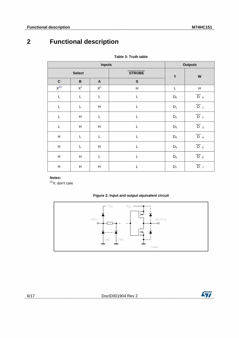
2 Functional description
Table 3: Truth table
Inputs Outputs
Select STROBE Y W
C B A S
X(1) X1 X1 H L H
L L L L D0 D 0
L L H L D1 D 1
L H L L D2 D 2
L H H L D3 D 3
H L L L D4 D 4
H L H L D5 D 5
H H L L D6 D 6
H H H L D7 D 7
Notes: (1)X: don’t care
Figure 2: Input and output equivalent circuit
6/17 DocID001904 Rev 2
M74HC151 Functional description
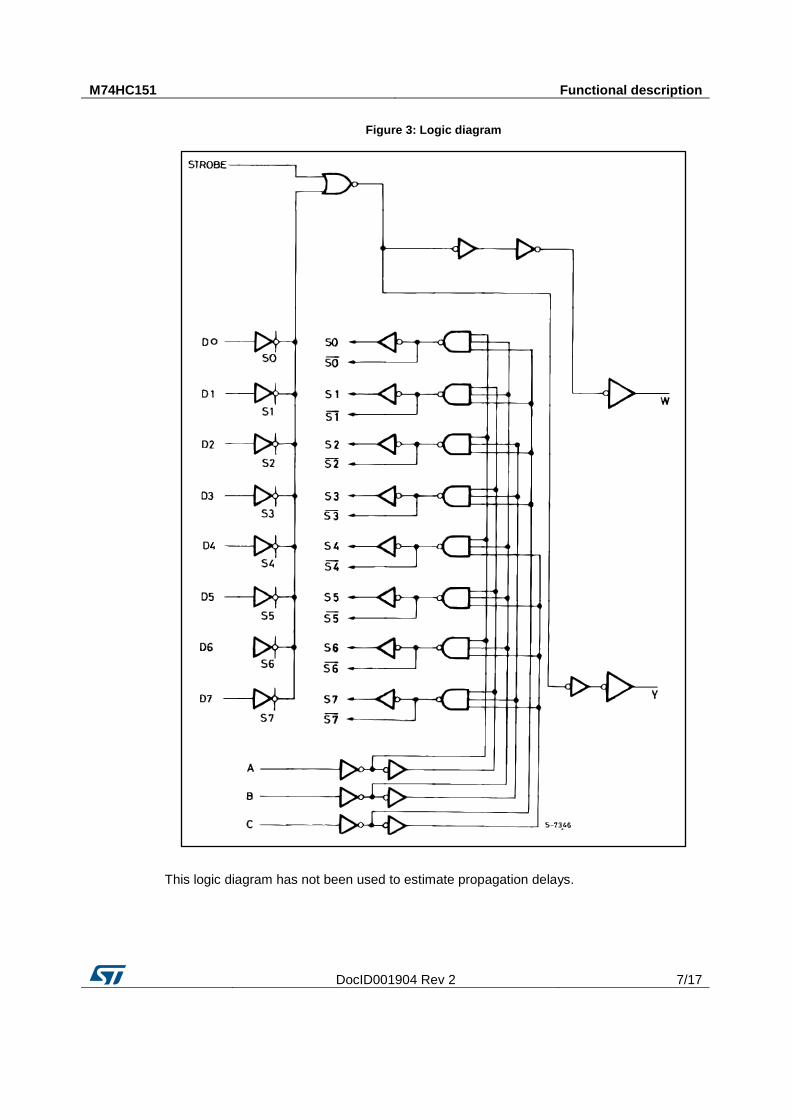
Figure 3: Logic diagram
This logic diagram has not been used to estimate propagation delays.
DocID001904 Rev 2 7/17

Electrical characteristics M74HC151
3 Electrical characteristics Stressing the device above the ratings listed in the "Absolute maximum ratings" table may cause permanent damage to the device. These are stress ratings only, and operation of the device at these or any other conditions above those indicated in the operating sections of this specification are not implied. Exposure to absolute maximum rating conditions for extended periods may affect device reliability.
Table 4: Absolute maximum ratings
Symbol Parameter Value Unit
VCC Supply voltage -0.5 to +7 V
VI DC input voltage -0.5 to VCC to +0.5 V
VO DC output voltage -0.5 to VCC to +0.5 V
IIK DC input diode current ±20 mA
IOK DC output diode current ±20 mA
IO DC output current ±25 mA
ICC or IGND DC VCC or ground current ±50 mA
PD Power dissipation 500(1) mW
Tstg Storage temperature -65 to +150 °C
TL Lead temperature (10 sec.) 300 °C
Notes: (1)500 mW at 65 °C; derate to 300 mW by 10 mW/°C from 65 °C to 85 °C
Table 5: Recommended operating conditions
Symbol Parameter Value Unit
VCC Supply voltage 2 to 6 V
VI Input voltage 0 to VCC V
VO Output voltage 0 to VCC V
Top Operating temperature -55 to 125 °C
tr, tf Input rise and fall time
VCC = 2.0 V 0 to 1000 ns
VCC = 4.5 V 0 to 500 ns
VCC = 6.0 V 0 to 400 ns
8/17 DocID001904 Rev 2
M74HC151 Electrical characteristics
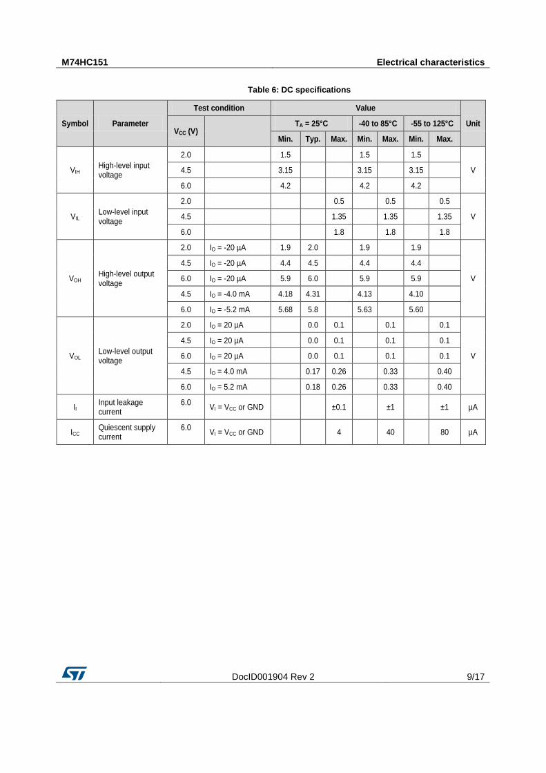
Table 6: DC specifications
Symbol Parameter
Test condition Value
Unit VCC (V)
TA = 25°C -40 to 85°C -55 to 125°C
Min. Typ. Max. Min. Max. Min. Max.
VIH High-level input voltage
2.0 1.5 1.5 1.5 V 4.5 3.15 3.15 3.15
6.0 4.2 4.2 4.2
VIL Low-level input voltage
2.0 0.5 0.5 0.5
V 4.5 1.35 1.35 1.35
6.0 1.8 1.8 1.8
VOH High-level output voltage
2.0 IO = -20 µA 1.9 2.0 1.9 1.9
V
4.5 IO = -20 µA 4.4 4.5 4.4 4.4 6.0 IO = -20 µA 5.9 6.0 5.9 5.9 4.5 IO = -4.0 mA 4.18 4.31 4.13 4.10 6.0 IO = -5.2 mA 5.68 5.8 5.63 5.60
VOL Low-level output voltage
2.0 IO = 20 µA 0.0 0.1 0.1 0.1
V
4.5 IO = 20 µA 0.0 0.1 0.1 0.1
6.0 IO = 20 µA 0.0 0.1 0.1 0.1
4.5 IO = 4.0 mA 0.17 0.26 0.33 0.40
6.0 IO = 5.2 mA 0.18 0.26 0.33 0.40
II Input leakage current
6.0 VI = VCC or GND ±0.1 ±1 ±1 µA
ICC Quiescent supply current
6.0 VI = VCC or GND 4 40 80 µA
DocID001904 Rev 2 9/17
Electrical characteristics M74HC151
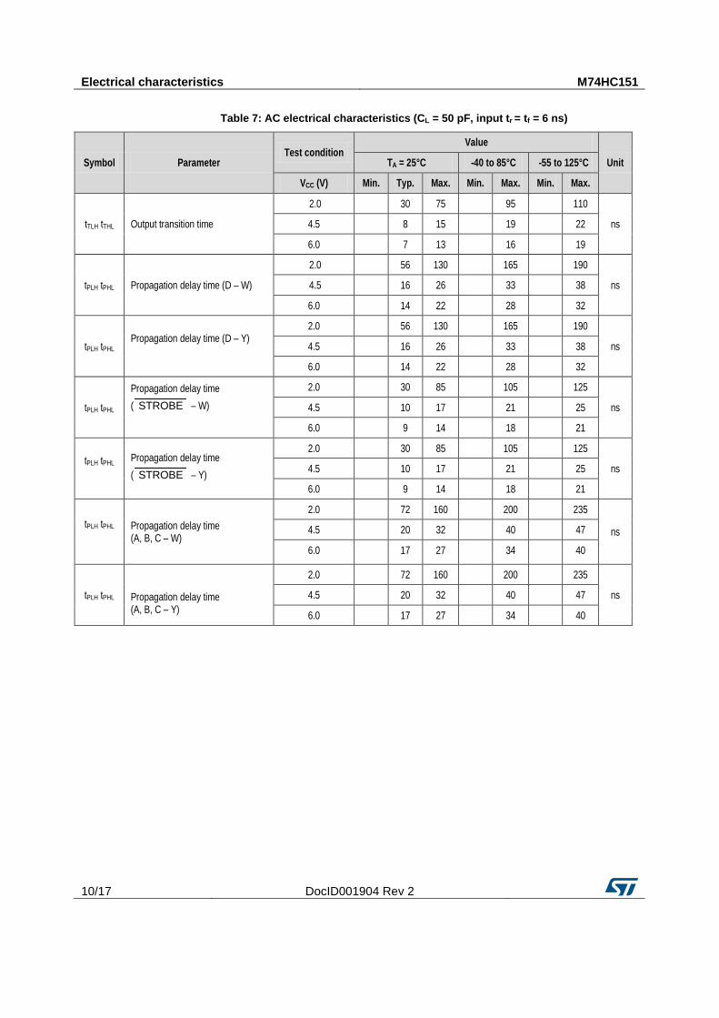
Table 7: AC electrical characteristics (CL = 50 pF, input tr = tf = 6 ns)
Symbol Parameter Test condition
Value
Unit TA = 25°C -40 to 85°C -55 to 125°C
VCC (V) Min. Typ. Max. Min. Max. Min. Max.
tTLH tTHL Output transition time
2.0 30 75 95 110
ns 4.5 8 15 19 22
6.0 7 13 16 19
tPLH tPHL Propagation delay time (D – W)
2.0 56 130 165 190
ns 4.5 16 26 33 38
6.0 14 22 28 32
tPLH tPHL Propagation delay time (D – Y)
2.0 56 130 165 190
ns 4.5 16 26 33 38
6.0 14 22 28 32
tPLH tPHL
Propagation delay time ( STROBE – W)
2.0 30 85 105 125
ns 4.5 10 17 21 25
6.0 9 14 18 21
tPLH tPHL
Propagation delay time ( STROBE – Y)
2.0 30 85 105 125
ns 4.5 10 17 21 25
6.0 9 14 18 21
tPLH tPHL
Propagation delay time (A, B, C – W)
2.0 72 160 200 235
ns 4.5 20 32 40 47
6.0 17 27 34 40
tPLH tPHL Propagation delay time (A, B, C – Y)
2.0 72 160 200 235
ns 4.5 20 32 40 47
6.0 17 27 34 40
10/17 DocID001904 Rev 2
M74HC151 Electrical characteristics
Table 8: Capacitive characteristics
Symbol Parameter Test
condition Value
Unit TA = 25°C -40 to 85°C -55 to 125°C
VCC (V) Min. Typ. Max. Min. Max. Min. Max.
CIN Input capacitance 5.0 5 10 10 10 pF
CPD Power dissipation capacitance(1)
5.0 63 pF
Notes: (1)CPD is defined as the value of the IC’s internal equivalent capacitance which is calculated from the operating current consumption without load (refer to the test circuit). The average operating current can be obtained by the following equation: ICC(opr) = CPD x VCC x fIN + ICC
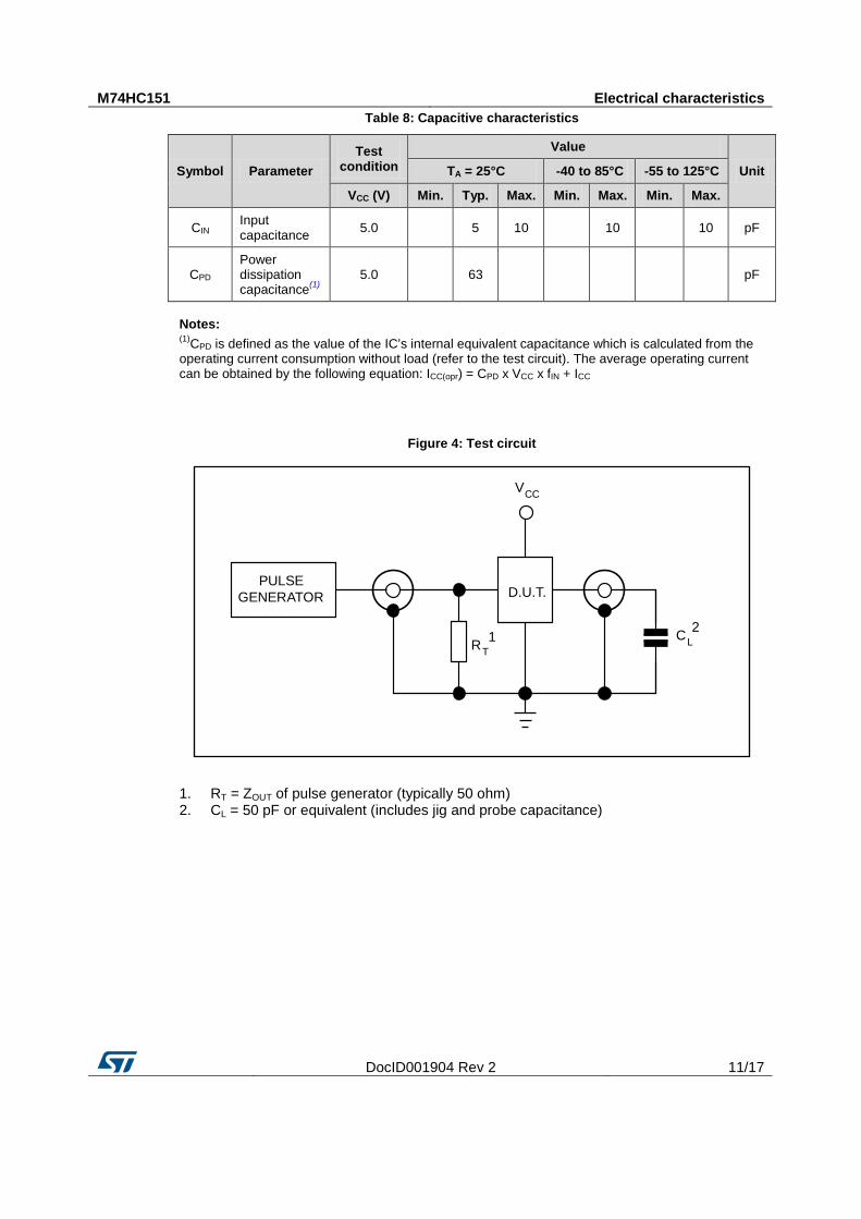
Figure 4: Test circuit
1. RT = ZOUT of pulse generator (typically 50 ohm) 2. CL = 50 pF or equivalent (includes jig and probe capacitance)
DocID001904 Rev 2 11/17
1RT
2CL
VCC
D.U.T.PULSE
GENERATOR

Electrical characteristics M74HC151
Figure 5: Waveform 1: propagation delay times (f = 1 MHz; 50% duty cycle)
Figure 6: Waveform 2: propagation delay times (f = 1 MHz; 50% duty cycle)
12/17 DocID001904 Rev 2
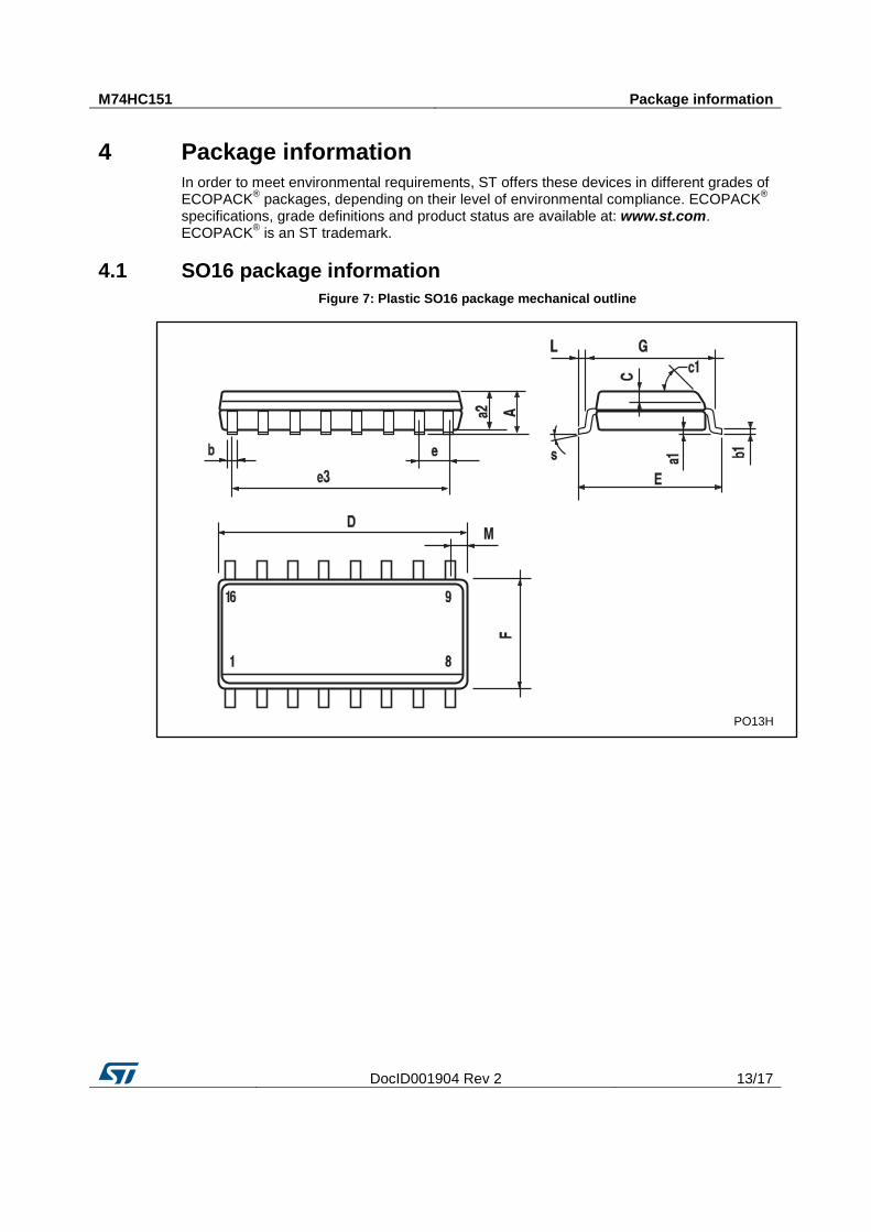
M74HC151 Package information
4 Package information In order to meet environmental requirements, ST offers these devices in different grades of ECOPACK® packages, depending on their level of environmental compliance. ECOPACK® specifications, grade definitions and product status are available at: www.st.com. ECOPACK® is an ST trademark.
4.1 SO16 package information Figure 7: Plastic SO16 package mechanical outline
DocID001904 Rev 2 13/17
PO13H
Package information M74HC151
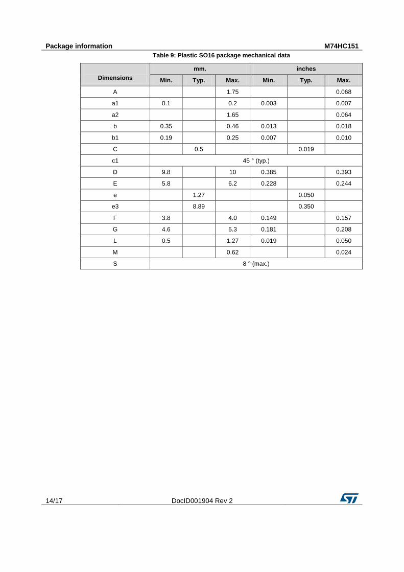
Table 9: Plastic SO16 package mechanical data
Dimensions
mm. inches
Min. Typ. Max. Min. Typ. Max.
A 1.75 0.068
a1 0.1 0.2 0.003 0.007
a2 1.65 0.064
b 0.35 0.46 0.013 0.018
b1 0.19 0.25 0.007 0.010
C 0.5 0.019
c1 45 ° (typ.)
D 9.8 10 0.385 0.393
E 5.8 6.2 0.228 0.244
e 1.27 0.050
e3 8.89 0.350
F 3.8 4.0 0.149 0.157
G 4.6 5.3 0.181 0.208
L 0.5 1.27 0.019 0.050
M 0.62 0.024
S 8 ° (max.)
14/17 DocID001904 Rev 2
M74HC151 Package information
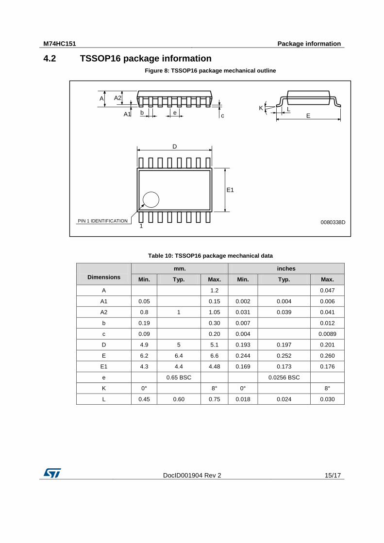
4.2 TSSOP16 package information Figure 8: TSSOP16 package mechanical outline
Table 10: TSSOP16 package mechanical data
Dimensions
mm. inches
Min. Typ. Max. Min. Typ. Max.
A 1.2 0.047
A1 0.05 0.15 0.002 0.004 0.006
A2 0.8 1 1.05 0.031 0.039 0.041
b 0.19 0.30 0.007 0.012
c 0.09 0.20 0.004 0.0089
D 4.9 5 5.1 0.193 0.197 0.201
E 6.2 6.4 6.6 0.244 0.252 0.260
E1 4.3 4.4 4.48 0.169 0.173 0.176
e 0.65 BSC 0.0256 BSC
K 0° 8° 0° 8°
L 0.45 0.60 0.75 0.018 0.024 0.030
DocID001904 Rev 2 15/17
c Eb
A2A
E1
D
1
A1LK
e
0080338DPIN 1 IDENTIFICATION
Revision history M74HC151
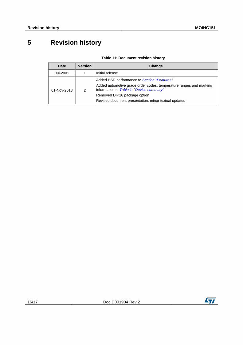
5 Revision history
Table 11: Document revision history
Date Version Change
Jul-2001 1 Initial release
01-Nov-2013 2
Added ESD performance to Section "Features" Added automotive grade order codes, temperature ranges and marking information to Table 1: "Device summary" Removed DIP16 package option Revised document presentation, minor textual updates
16/17 DocID001904 Rev 2
M74HC151
Please Read Carefully
Information in this document is provided solely in connection with ST products. STMicroelectronics NV and its subsidiaries ("ST") reserve the right to make changes, corrections, modifications or improvements, to this document, and the products and services described herein at any time, without notice.
All ST products are sold pursuant to ST’s terms and conditions of sale.
Purchasers are solely responsible for the choice, selection and use of the ST products and services described herein, and ST assumes no liability whatsoever relating to the choice, selection or use of the ST products and services described herein.
No license, express or implied, by estoppel or otherwise, to any intellectual property rights is granted under this document. If any part of this document refers to any third party products or services it shall not be deemed a license grant by ST for the use of such third party products or services, or any intellectual property contained therein or considered as a warranty covering the use in any manner whatsoever of such third party products or services or any intellectual property contained therein.
UNLESS OTHERWISE SET FORTH IN ST’S TERMS AND CONDITIONS OF SALE ST DISCLAIMS ANY EXPRESS OR IMPLIED WARRANTY WITH RESPECT TO THE USE AND/OR SALE OF ST PRODUCTS INCLUDING WITHOUT LIMITATION IMPLIED WARRANTIES OF MERCHANTABILITY, FITNESS FOR A PARTICULAR PURPOSE (AND THEIR EQUIVALENTS UNDER THE LAWS OF ANY JURISDICTION), OR INFRINGEMENT OF ANY PATENT, COPYRIGHT OR OTHER INTELLECTUAL PROPERTY RIGHT.
ST PRODUCTS ARE NOT DESIGNED OR AUTHORIZED FOR USE IN: (A) SAFETY CRITICAL APPLICATIONS SUCH AS LIFE SUPPORTING, ACTIVE IMPLANTED DEVICES OR SYSTEMS WITH PRODUCT FUNCTIONAL SAFETY REQUIREMENTS; (B) AERONAUTIC APPLICATIONS; (C) AUTOMOTIVE APPLICATIONS OR ENVIRONMENTS, AND/OR (D) AEROSPACE APPLICATIONS OR ENVIRONMENTS. WHERE ST PRODUCTS ARE NOT DESIGNED FOR SUCH USE, THE PURCHASER SHALL USE PRODUCTS AT PURCHASER’S SOLE RISK, EVEN IF ST HAS BEEN INFORMED IN WRITING OF SUCH USAGE, UNLESS A PRODUCT IS EXPRESSLY DESIGNATED BY ST AS BEING INTENDED FOR "AUTOMOTIVE, AUTOMOTIVE SAFETY OR MEDICAL" INDUSTRY DOMAINS ACCORDING TO ST PRODUCT DESIGN SPECIFICATIONS. PRODUCTS FORMALLY ESCC, QML OR JAN QUALIFIED ARE DEEMED SUITABLE FOR USE IN AEROSPACE BY THE CORRESPONDING GOVERNMENTAL AGENCY.
Resale of ST products with provisions different from the statements and/or technical features set forth in this document shall immediately void any warranty granted by ST for the ST product or service described herein and shall not create or extend in any manner whatsoever, any liability of ST.
ST and the ST logo are trademarks or registered trademarks of ST in various countries.
Information in this document supersedes and replaces all information previously supplied.
The ST logo is a registered trademark of STMicroelectronics. All other names are the property of their respective owners.
© 2013 STMicroelectronics - All rights reserved
STMicroelectronics group of companies
Australia - Belgium - Brazil - Canada - China - Czech Republic - Finland - France - Germany - Hong Kong - India - Israel - Italy - Japan - Malaysia - Malta - Morocco - Philippines - Singapore - Spain - Sweden - Switzerland - United Kingdom - United
States of America
www.st.com
DocID001904 Rev 2 17/17