80386dx 32-bit microprocessor - data device … · ture includes address translation registers,...
TRANSCRIPT

1
Mem
ory
All data sheets are subject to change without notice
(631) 567-5600 - Fax: (631) 567-7358 - www.ddc-web.com
32-Bit Microprocessor80386DX
©2001 DDCAll rights reserved.
12.17.01 Rev11000557
FEATURES:• 32-Bit microprocessor• RAD-PAK® radiation-hardened against natural space radia-
tion• Total dose hardness:
- >100 Krad (Si), dependent upon space mission• Single event effect:
- SELTH = 37-60 MeV/mg/cm2
- SEUTH = 3.4 MeV/mg/cm2
- SEU Cross section 1E-3 cm2/bit• Package:
- 164 Pin RAD-PAK® quad flat pack• 8, 16, 32-Bit data types• 8 general purpose 32-Bit registers• Hardware debugging support• Very large address space:
- 4 gigabyte physical- 64 terabyte Virtual - 4 gigabyte maximum segment size
• Integrated memory management unit- Virtual memory support- Four levels of protection- Fully compatible with 80C286
• Optimized for system development- Pipelined instructions- On-chip caches support address translation- 32 megabytes/sec bus bandwidth
DESCRIPTION:DDC's 80386DX high performance 32-bitmicroprocessor features a geater than 100 krad (Si) total dosetolerance, dependent upon space mission. It is designed forvery high performance and multitasking operating systems.The integrated memory management and protection architec-ture includes address translation registers, multitasking hard-ware and a protection mechanism to support operatingsystems. The 80386DX allows simultaneous running of multi-ple operations. In addition, the 80386DX is capable of execu-tion at sustained rates of between 3 and 4 million instructionsper second. It offers new testability and debugging features,including a self-test and direct access to the page translationcache.
DDC's patented RAD-PAK® packaging technol-ogy incorporates radiation shielding in the microcircuit pack-age. It eliminates the need for box shielding while providingthe required radiation shielding for a lifetime in orbit or spacemission. In a GEO orbit, RAD-PAK provides greater than 100krad (Si) radiation dose tolerance. This product is availablewith screening up to Class S.
Logic Diagram
22 144
14521
62
63 103
104
Mem
ory
2All data sheets are subject to change without notice
©2001 DDCAll rights reserved.
32-Bit Microprocessor 80386DX
12.17.01 Rev11000557
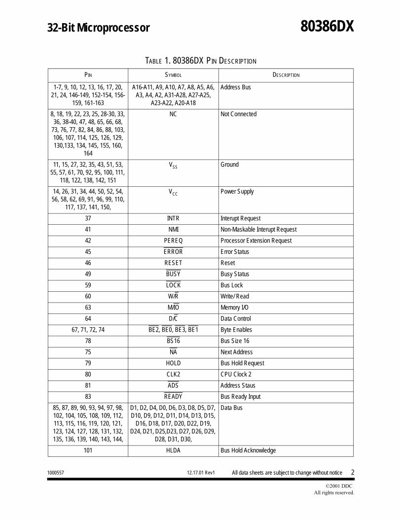
TABLE 1. 80386DX PIN DESCRIPTION
PIN SYMBOL DESCRIPTION
1-7, 9, 10, 12, 13, 16, 17, 20, 21, 24, 146-149, 152-154, 156-
159, 161-163
A16-A11, A9, A10, A7, A8, A5, A6, A3, A4, A2, A31-A28, A27-A25,
A23-A22, A20-A18
Address Bus
8, 18, 19, 22, 23, 25, 28-30, 33, 36, 38-40, 47, 48, 65, 66, 68,
73, 76, 77, 82, 84, 86, 88, 103, 106, 107, 114, 125, 126, 129, 130,133, 134, 145, 155, 160,
164
NC Not Connected
11, 15, 27, 32, 35, 43, 51, 53, 55, 57, 61, 70, 92, 95, 100, 111,
118, 122, 138, 142, 151
VSS Ground
14, 26, 31, 34, 44, 50, 52, 54, 56, 58, 62, 69, 91, 96, 99, 110,
117, 137, 141, 150,
VCC Power Supply
37 INTR Interupt Request
41 NMI Non-Maskable Interupt Request
42 PEREQ Processor Extension Request
45 ERROR Error Status
46 RESET Reset
49 BUSY Busy Status
59 LOCK Bus Lock
60 W/R Write/ Read
63 M/IO Memory I/O
64 D/C Data Control
67, 71, 72, 74 BE2, BE0, BE3, BE1 Byte Enables
78 BS16 Bus Size 16
75 NA Next Address
79 HOLD Bus Hold Request
80 CLK2 CPU Clock 2
81 ADS Address Staus
83 READY Bus Ready Input
85, 87, 89, 90, 93, 94, 97, 98, 102, 104, 105, 108, 109, 112, 113, 115, 116, 119, 120, 121, 123, 124, 127, 128, 131, 132, 135, 136, 139, 140, 143, 144,
D1, D2, D4, D0, D6, D3, D8, D5, D7, D10, D9, D12, D11, D14, D13, D15,
D16, D18, D17, D20, D22, D19, D24, D21, D25,D23, D27, D26, D29,
D28, D31, D30,
Data Bus
101 HLDA Bus Hold Acknowledge
Mem
ory
3All data sheets are subject to change without notice
©2001 DDCAll rights reserved.
32-Bit Microprocessor 80386DX
12.17.01 Rev11000557
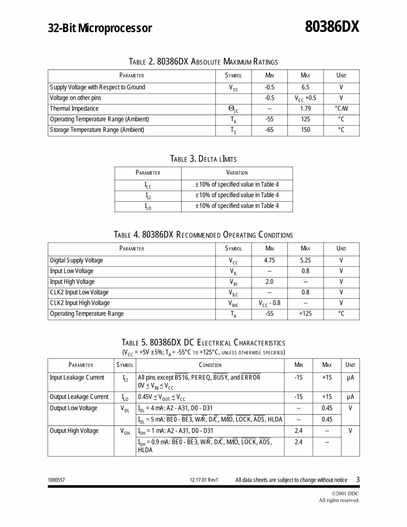
TABLE 2. 80386DX ABSOLUTE MAXIMUM RATINGS
PARAMETER SYMBOL MIN MAX UNIT
Supply Voltage with Respect to Ground VSS -0.5 6.5 V
Voltage on other pins -0.5 VCC +0.5 V
Thermal Impedance ΘJC -- 1.79 °C/W
Operating Temperature Range (Ambient) TA -55 125 °C
Storage Temperature Range (Ambient) TS -65 150 °C
TABLE 3. DELTA LIMITS
PARAMETER VARIATION
ICC ±10% of specified value in Table 4
ILI ±10% of specified value in Table 4
ILO ±10% of specified value in Table 4
TABLE 4. 80386DX RECOMMENDED OPERATING CONDITIONS
PARAMETER SYMBOL MIN MAX UNIT
Digital Supply Voltage VCC 4.75 5.25 V
Input Low Voltage VIL -- 0.8 V
Input High Voltage VIH 2.0 -- V
CLK2 Input Low Voltage VILC -- 0.8 V
CLK2 Input High Voltage VIHC VCC - 0.8 -- V
Operating Temperature Range TA -55 +125 °C
TABLE 5. 80386DX DC ELECTRICAL CHARACTERISTICS(VCC = +5V ±5%; TA = -55°C TO +125°C, UNLESS OTHERWISE SPECIFIED)
PARAMETER SYMBOL CONDITION MIN MAX UNIT
Input Leakage Current ILI All pins except BS16, PEREQ, BUSY, and ERROR0V < VIN < VCC
-15 +15 µ A
Output Leakage Current ILO 0.45V < VOUT < VCC -15 +15 µ A
Output Low Voltage VOL IOL = 4 mA: A2 - A31, D0 - D31 -- 0.45 V
IOL = 5 mA: BE0 - BE3, W/R, D/C, M/IO, LOCK, ADS, HLDA -- 0.45
Output High Voltage VOH IOH = 1 mA: A2 - A31, D0 - D31 2.4 -- V
IOH = 0.9 mA: BE0 - BE3, W/R, D/C, M/IO, LOCK, ADS, HLDA
2.4 --
Mem
ory
4All data sheets are subject to change without notice
©2001 DDCAll rights reserved.
32-Bit Microprocessor 80386DX
12.17.01 Rev11000557
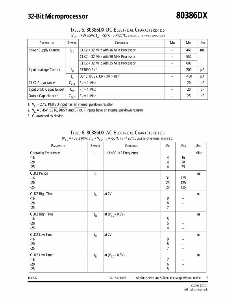
Power Supply Current ICC CLK2 = 32 MHz with 16 MHz Processor -- 460 mA
CLK2 = 32 MHz with 20 MHz Processor -- 550
CLK2 = 32 MHz with 25 MHz Processor -- 680
Input Leakage Current IIH PEREQ Pin1 -- 200 µ A
IIL BS16, BUSY, ERROR Pins2 -- -400 µ A
CLK2 Capacitance3 CCLK FC = 1 MHz -- 20 pF
Input or I/O Capacitance1 CIN FC = 1 MHz -- 20 pF
Output Capacitance1 COUT FC = 1 MHz -- 25 pF
1. VIH = 2.4V. PEREQ input has an internal pulldown resistor.
2. VIL = 0.45V. BS16, BUSY and ERROR inputs have an internal pulldown resistor.
3. Guaranteed by design.
TABLE 6. 80386DX AC ELECTRICAL CHARACTERISTICS(VCC = +5V ±10%; VPP = VSS; TA = -55°C TO +125°C, UNLESS OTHERWISE SPECIFIED)
PARAMETER SYMBOL CONDITION MIN MAX UNIT
Operating Frequency-16-20-25
-- Half of CLK2 Frequency444
162025
MHz
CLK2 Period-16-20-25
t1312520
125125125
ns
CLK2 High Time-16-20-25
t2a at 2V987
------
ns
CLK2 High Time1
-16-20-25
t2b at (VCC - 0.8V)554
------
ns
CLK2 Low Time-16-20-25
t3a at 2V987
------
ns
CLK2 Low Time1
-16-20-25
t3b at (VCC - 0.8V)765
------
ns
TABLE 5. 80386DX DC ELECTRICAL CHARACTERISTICS(VCC = +5V ±5%; TA = -55°C TO +125°C, UNLESS OTHERWISE SPECIFIED)
PARAMETER SYMBOL CONDITION MIN MAX UNIT
Mem
ory
5All data sheets are subject to change without notice
©2001 DDCAll rights reserved.
32-Bit Microprocessor 80386DX
12.17.01 Rev11000557
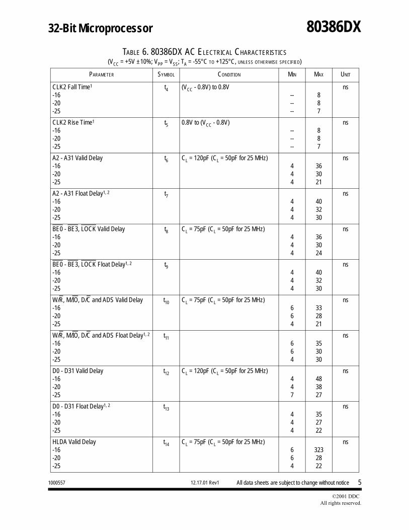
CLK2 Fall Time1
-16-20-25
t4 (VCC - 0.8V) to 0.8V------
887
ns
CLK2 Rise Time1
-16-20-25
t5 0.8V to (VCC - 0.8V)------
887
ns
A2 - A31 Valid Delay-16-20-25
t6 CL = 120pF (CL = 50pF for 25 MHz)444
363021
ns
A2 - A31 Float Delay1, 2
-16-20-25
t7444
403230
ns
BE0 - BE3, LOCK Valid Delay-16-20-25
t8 CL = 75pF (CL = 50pF for 25 MHz)444
363024
ns
BE0 - BE3, LOCK Float Delay1, 2
-16-20-25
t9444
403230
ns
W/R, M/IO, D/C and ADS Valid Delay-16-20-25
t10 CL = 75pF (CL = 50pF for 25 MHz)664
332821
ns
W/R, M/IO, D/C and ADS Float Delay1, 2
-16-20-25
t11664
353030
ns
D0 - D31 Valid Delay-16-20-25
t12 CL = 120pF (CL = 50pF for 25 MHz)447
483827
ns
D0 - D31 Float Delay1, 2
-16-20-25
t13444
352722
ns
HLDA Valid Delay-16-20-25
t14 CL = 75pF (CL = 50pF for 25 MHz)664
3232822
ns
TABLE 6. 80386DX AC ELECTRICAL CHARACTERISTICS(VCC = +5V ±10%; VPP = VSS; TA = -55°C TO +125°C, UNLESS OTHERWISE SPECIFIED)
PARAMETER SYMBOL CONDITION MIN MAX UNIT

Mem
ory
6All data sheets are subject to change without notice
©2001 DDCAll rights reserved.
32-Bit Microprocessor 80386DX
12.17.01 Rev11000557
N/A Setup Time-16-20-25
t151197
------
ns
N/A Hold Time-16-20-25
t1614143
------
ns
BS16 Setup Time-16-20-25
t1713137
------
ns
BS16 Hold Time-16-20-25
t1821213
------
ns
READY Setup Time-16-20-25
t1921129
------
ns
READY Hold Time-16-20-25
t20444
------
ns
D0 - D31 Read Setup Delay-16-20-25
t2111116
------
ns
D0 - D31 Read Hold Delay-16-20-25
t22665
------
ns
HOLD Setup Time-16-20-25
t23261715
------
ns
HOLD Hold Time-16-20-25
t24553
------
ns
RESET Setup Time-16-20-25
t25101010
------
ns
TABLE 6. 80386DX AC ELECTRICAL CHARACTERISTICS(VCC = +5V ±10%; VPP = VSS; TA = -55°C TO +125°C, UNLESS OTHERWISE SPECIFIED)
PARAMETER SYMBOL CONDITION MIN MAX UNIT

Mem
ory
7All data sheets are subject to change without notice
©2001 DDCAll rights reserved.
32-Bit Microprocessor 80386DX
12.17.01 Rev11000557
RESET Hold Time-16-20-25
t26443
------
ns
NMI, INTR Setup Time3
-16-20-25
t2716166
------
ns
NMI, INTR Hold Time3
-16-20-25
t2816166
------
ns
REREQ, ERROR, BUSY Setup Time3
-16-20-25
t2916146
------
ns
REREQ, ERROR, BUSY Hold Time3
-16-20-25
t30555
------
ns
1. Guaranteed by design.
2. Float condition occurs when maximum when output current becomes less than ILO in magnitude.
3. These inputs are allowed to be asynchronous to CLK2. The setup and hold specifications are given for testing purposes, to assure recognition within a specific CLK2 period.
TABLE 6. 80386DX AC ELECTRICAL CHARACTERISTICS(VCC = +5V ±10%; VPP = VSS; TA = -55°C TO +125°C, UNLESS OTHERWISE SPECIFIED)
PARAMETER SYMBOL CONDITION MIN MAX UNIT
Mem
ory
8All data sheets are subject to change without notice
©2001 DDCAll rights reserved.
32-Bit Microprocessor 80386DX
12.17.01 Rev11000557
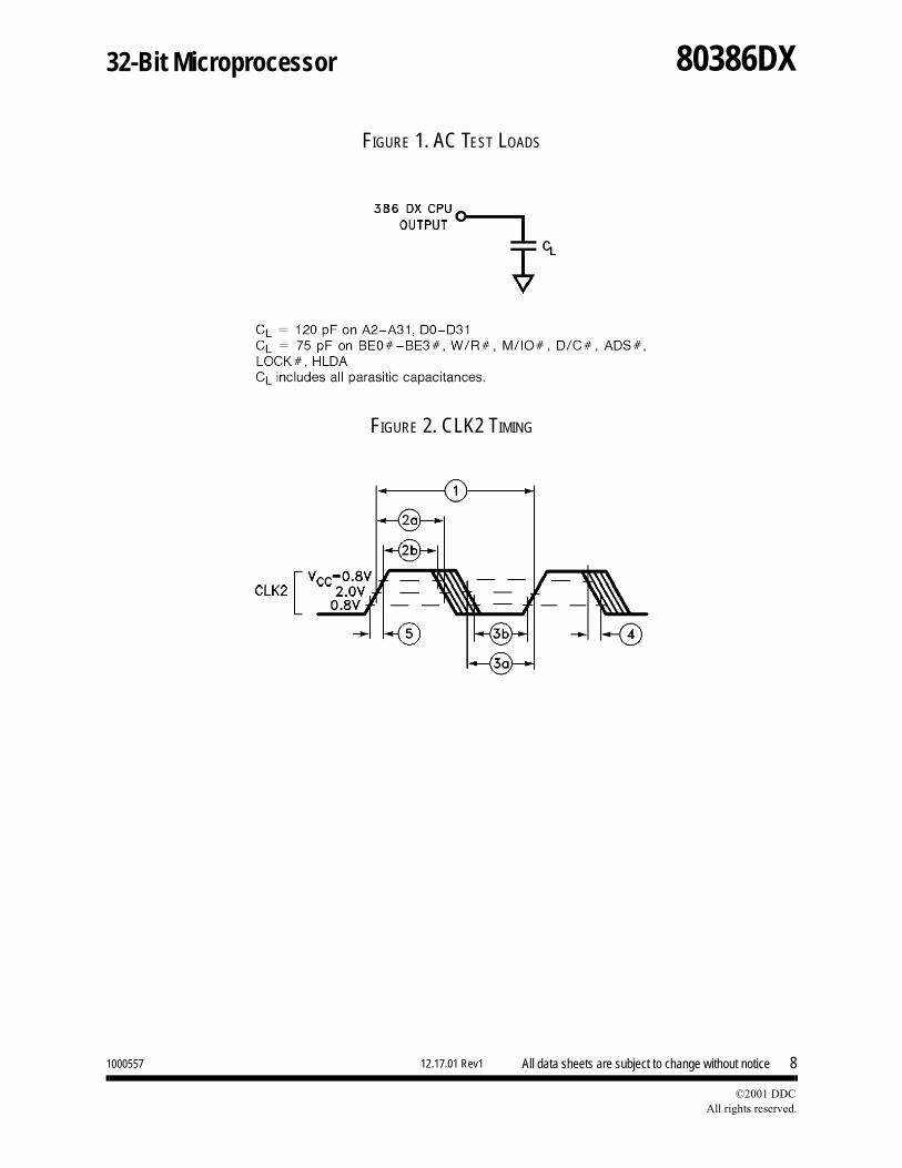
FIGURE 1. AC TEST LOADS
FIGURE 2. CLK2 TIMING

Mem
ory
9All data sheets are subject to change without notice
©2001 DDCAll rights reserved.
32-Bit Microprocessor 80386DX
12.17.01 Rev11000557
FIGURE 3. INPUT SETUP AND HOLD TIME
Mem
ory
10All data sheets are subject to change without notice
©2001 DDCAll rights reserved.
32-Bit Microprocessor 80386DX
12.17.01 Rev11000557
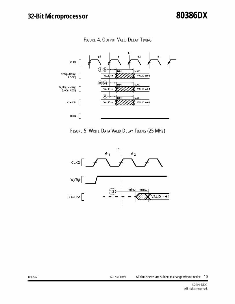
FIGURE 4. OUTPUT VALID DELAY TIMING
FIGURE 5. WRITE DATA VALID DELAY TIMING (25 MHZ)
Mem
ory
11All data sheets are subject to change without notice
©2001 DDCAll rights reserved.
32-Bit Microprocessor 80386DX
12.17.01 Rev11000557
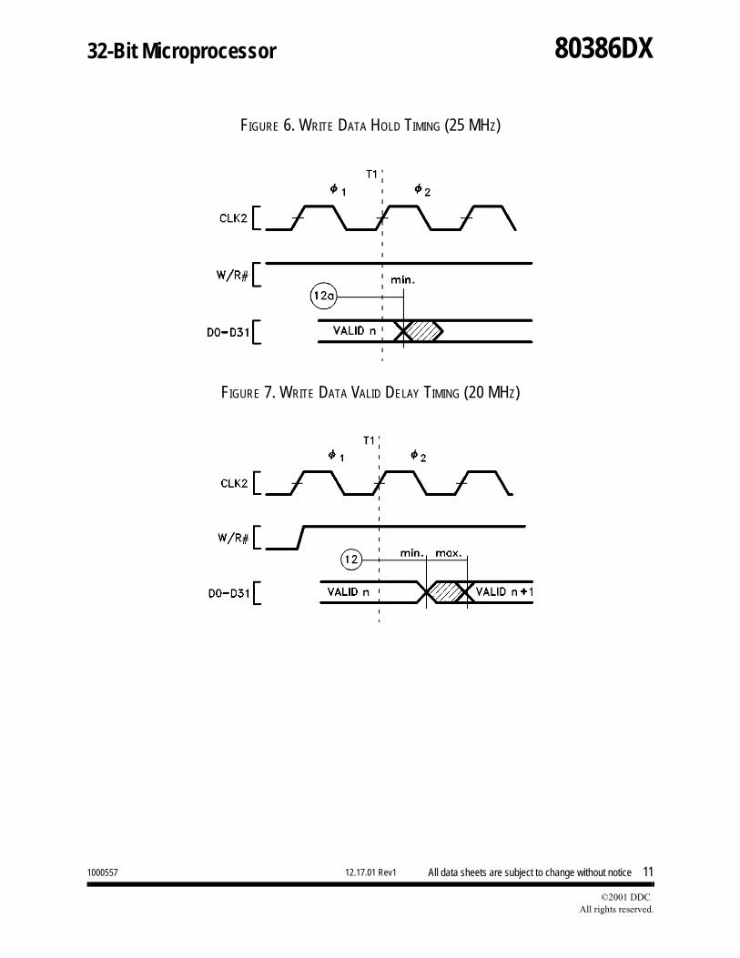
FIGURE 6. WRITE DATA HOLD TIMING (25 MHZ)
FIGURE 7. WRITE DATA VALID DELAY TIMING (20 MHZ)
Mem
ory
12All data sheets are subject to change without notice
©2001 DDCAll rights reserved.
32-Bit Microprocessor 80386DX
12.17.01 Rev11000557
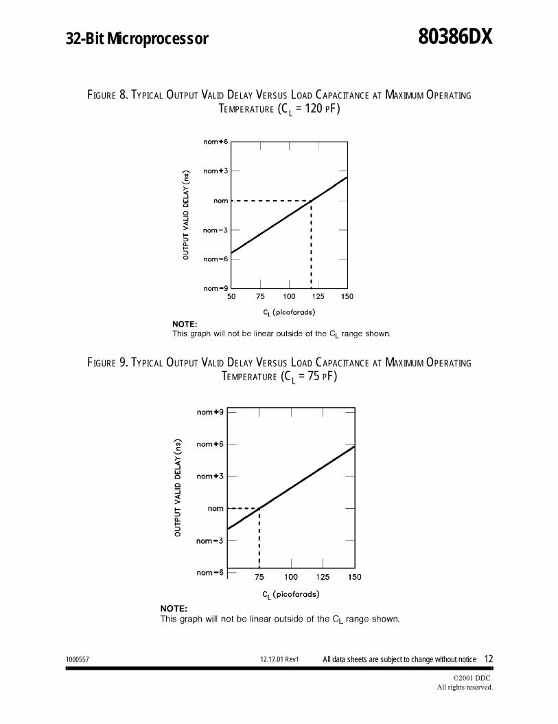
FIGURE 8. TYPICAL OUTPUT VALID DELAY VERSUS LOAD CAPACITANCE AT MAXIMUM OPERATING TEMPERATURE (CL = 120 PF)
FIGURE 9. TYPICAL OUTPUT VALID DELAY VERSUS LOAD CAPACITANCE AT MAXIMUM OPERATING TEMPERATURE (CL = 75 PF)
Mem
ory
13All data sheets are subject to change without notice
©2001 DDCAll rights reserved.
32-Bit Microprocessor 80386DX
12.17.01 Rev11000557
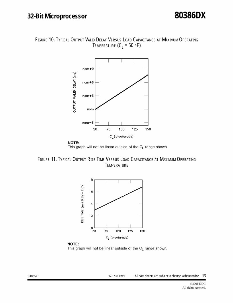
FIGURE 10. TYPICAL OUTPUT VALID DELAY VERSUS LOAD CAPACITANCE AT MAXIMUM OPERATING TEMPERATURE (CL = 50 PF)
FIGURE 11. TYPICAL OUTPUT RISE TIME VERSUS LOAD CAPACITANCE AT MAXIMUM OPERATING TEMPERATURE

Mem
ory
14All data sheets are subject to change without notice
©2001 DDCAll rights reserved.
32-Bit Microprocessor 80386DX
12.17.01 Rev11000557
FIGURE 12. OUTPUT FLOAT DELAY AND HLDA AND DELAY TIMING
FIGURE 13. RESET SETUP AND HOLD TIMING, AND INTERNAL PHASE
Mem
ory
15All data sheets are subject to change without notice
©2001 DDCAll rights reserved.
32-Bit Microprocessor 80386DX
12.17.01 Rev11000557
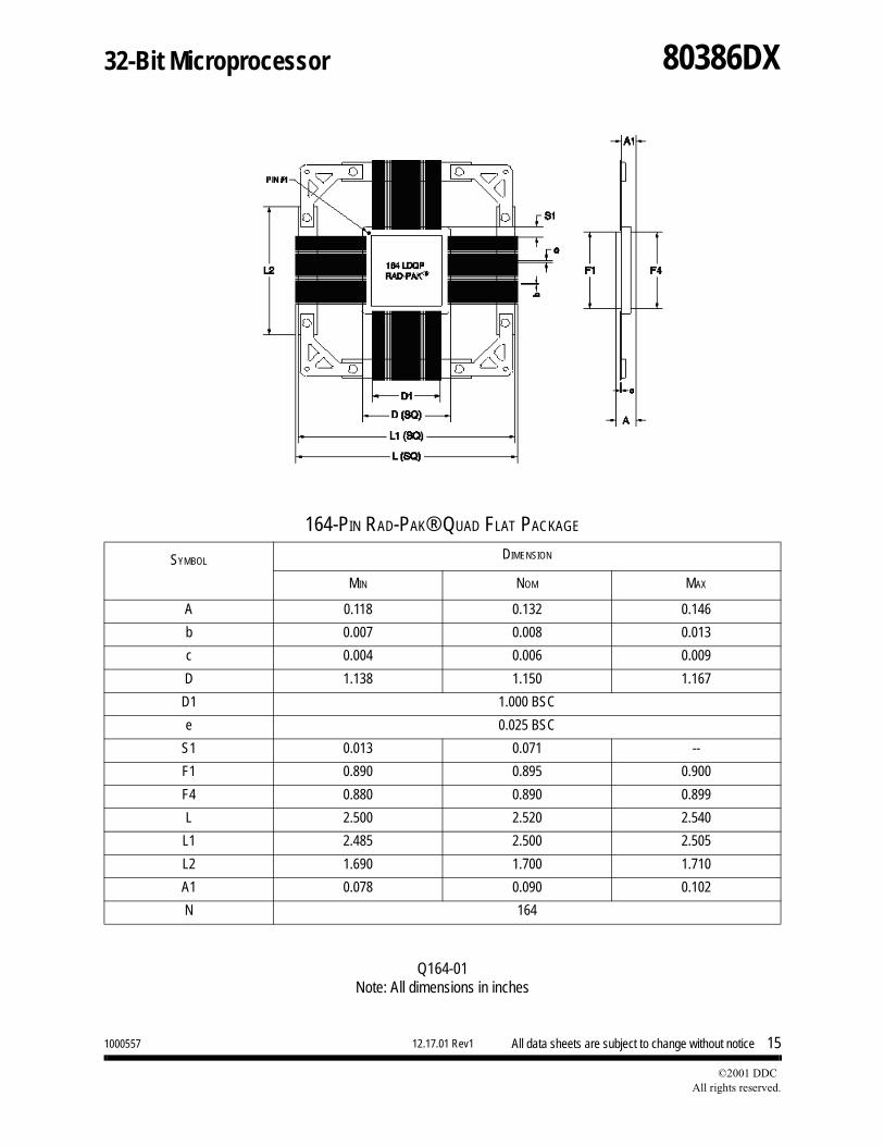
Q164-01Note: All dimensions in inches
164-PIN RAD-PAK® QUAD FLAT PACKAGE
SYMBOL DIMENSION
MIN NOM MAX
A 0.118 0.132 0.146
b 0.007 0.008 0.013
c 0.004 0.006 0.009
D 1.138 1.150 1.167
D1 1.000 BSC
e 0.025 BSC
S1 0.013 0.071 --
F1 0.890 0.895 0.900
F4 0.880 0.890 0.899
L 2.500 2.520 2.540
L1 2.485 2.500 2.505
L2 1.690 1.700 1.710
A1 0.078 0.090 0.102
N 164

Mem
ory
16All data sheets are subject to change without notice
©2001 DDCAll rights reserved.
32-Bit Microprocessor 80386DX
12.17.01 Rev11000557
Important Notice:
These data sheets are created using the chip manufacturer’s published specifications. DDC verifiesfunctionality by testing key parameters either by 100% testing, sample testing or characterization.
The specifications presented within these data sheets represent the latest and most accurate information available todate. However, these specifications are subject to change without notice and DDC assumes noresponsibility for the use of this information.
DDC's products are not authorized for use as critical components in life support devices or systemswithout express written approval from DDC.
Any claim against DDC must be made within 90 days from the date of shipment from DDC. DDC's liability shall be limited to replacement of defective parts.
Mem
ory
17All data sheets are subject to change without notice
©2001 DDCAll rights reserved.
32-Bit Microprocessor 80386DX
12.17.01 Rev11000557
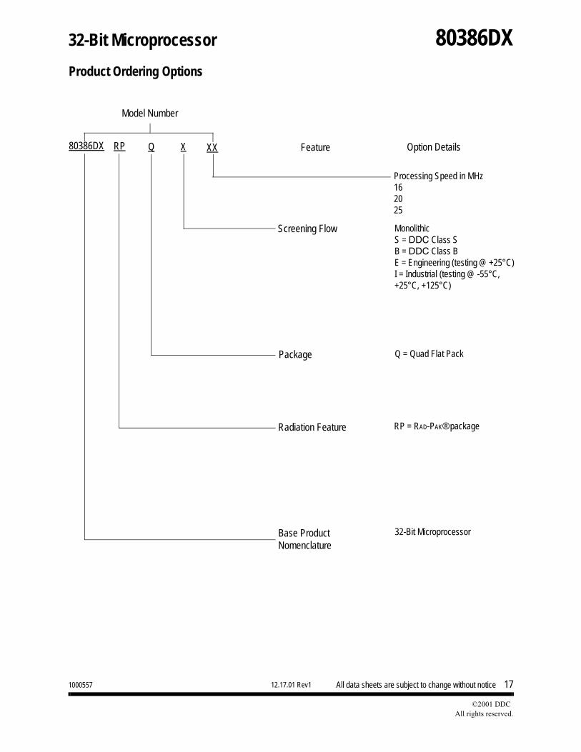
Product Ordering Options
Model Number
Feature Option Details80386DX RP Q X
Screening Flow
Package
Radiation Feature
Base Product Nomenclature
MonolithicS = DDC Class SB = DDC Class BE = Engineering (testing @ +25°C)I = Industrial (testing @ -55°C, +25°C, +125°C)
Q = Quad Flat Pack
RP = RAD-PAK® package
32-Bit Microprocessor
XX
Processing Speed in MHz162025