(83-313) lecture 5: designing sequential logic circuits · sequential logic •sequential circuits...
TRANSCRIPT

Disclaimer: This course was prepared, in its entirety, by Adam Teman. Many materials were copied from sources freely available on the internet. When possible, these sources have been cited;
however, some references may have been cited incorrectly or overlooked. If you feel that a picture, graph, or code example has been copied from you and either needs to be cited or removed,
please feel free to email [email protected] and I will address this as soon as possible.
Digital Integrated Circuits(83-313)
Lecture 5:
Designing SequentialLogic Circuits
Semester B, 2016-17
Lecturer: Dr. Adam Teman
TAs: Itamar Levi, Robert Giterman
26 April 2017
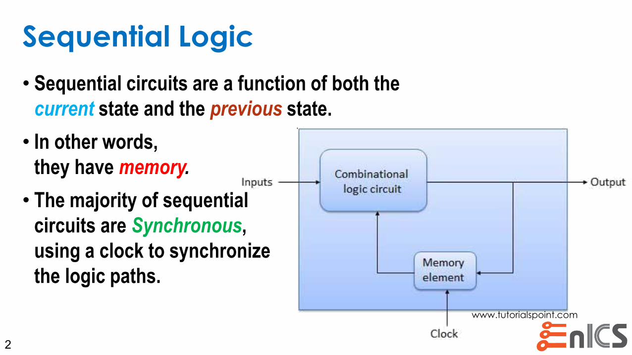
Sequential Logic
• Sequential circuits are a function of both the
current state and the previous state.
• In other words,
they have memory.
• The majority of sequential
circuits are Synchronous,
using a clock to synchronize
the logic paths.
2
www.tutorialspoint.com
Lecture Content
3

Why use Sequential Logic?
4
Explanation through example
• We will look at two examples:
• An accumulator circuit, where sequential
methods are essential to eliminate races.
• A pipelined system, where sequential
methods improve throughput.
5
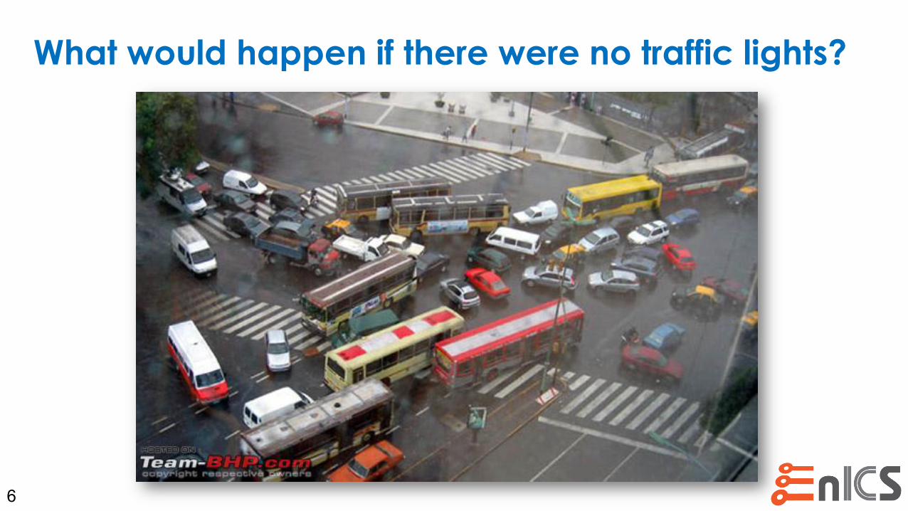
What would happen if there were no traffic lights?
6

Accumulator Example
• An accumulator is a register that sums a list of numbers.
Therefore, it feeds back the output back to the input.
• Without a register, there would be the possibility that
the input would change before the calculation was finished.
• We need to delay the output
until the original calculation
is finished.
7
+IN
OUT001
001
01
1+1=0 c1
XX0 c10
X00 c10
011
01+10=11
Accumulator Example
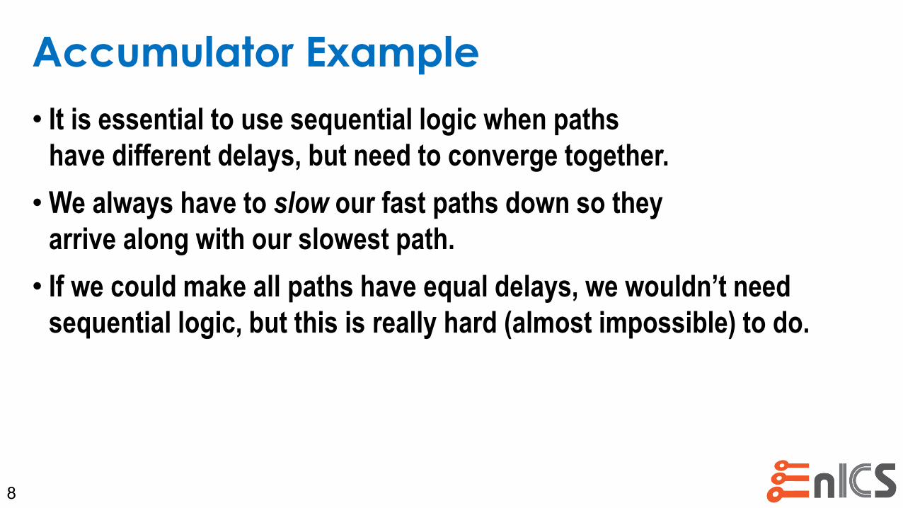
• It is essential to use sequential logic when paths
have different delays, but need to converge together.
• We always have to slow our fast paths down so they
arrive along with our slowest path.
• If we could make all paths have equal delays, we wouldn’t need
sequential logic, but this is really hard (almost impossible) to do.
8

Laundry Example
• Small laundry has one washer, one dryer and one operator,
it takes 90 minutes to finish one load:
• Washer takes 30 minutes
• Dryer takes 40 minutes
• “operator folding” takes 20 minutes
9
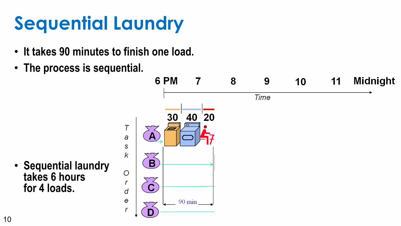
Sequential Laundry
• It takes 90 minutes to finish one load.
• The process is sequential.
• Sequential laundry takes 6 hours for 4 loads.
10

Pipelined Laundry
• Every 40 minutes a new load starts and a new load ends.
• Pipelined laundry
takes 3.5 hours
for 4 loads
11
Pipelining Data
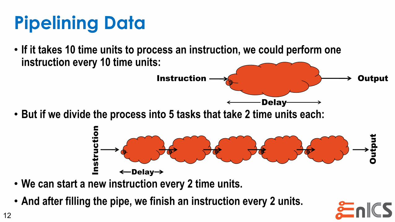
• If it takes 10 time units to process an instruction, we could perform one instruction every 10 time units:
• But if we divide the process into 5 tasks that take 2 time units each:
• We can start a new instruction every 2 time units.
• And after filling the pipe, we finish an instruction every 2 units.12
Instruction
Delay
Output
Instr
ucti
on
Delay
Ou
tput
Pipelining Data
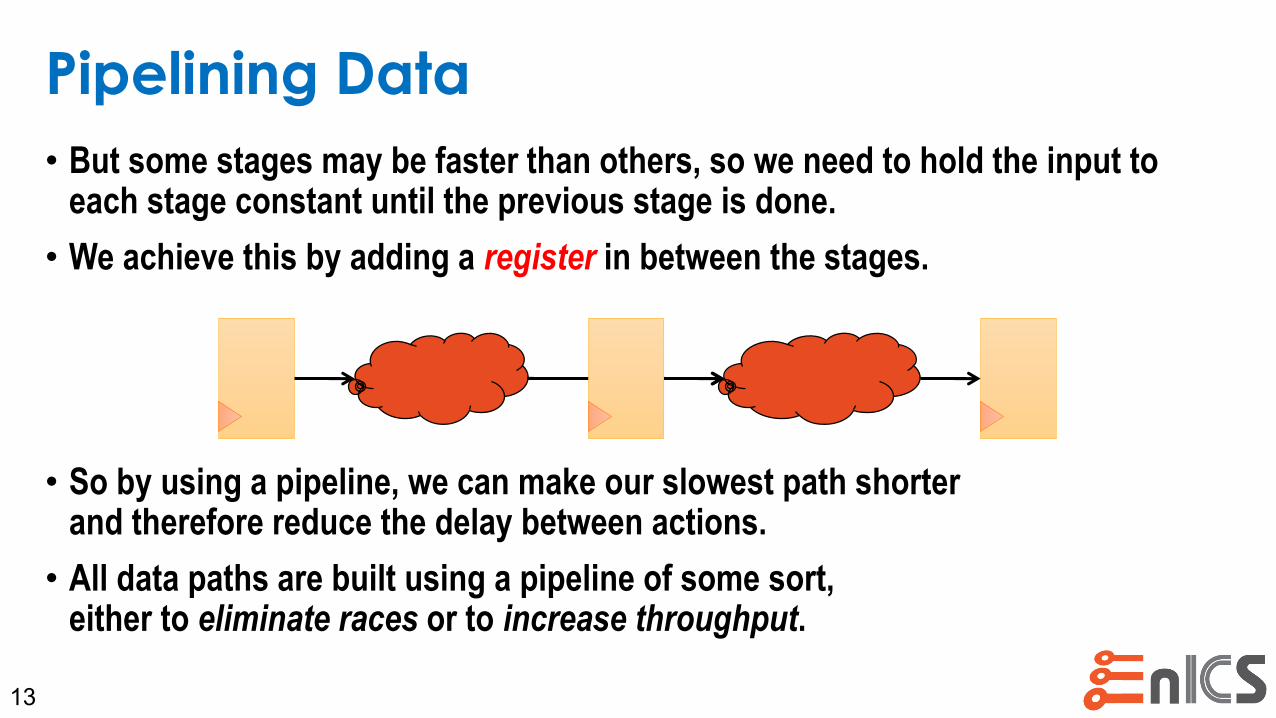
• But some stages may be faster than others, so we need to hold the input to each stage constant until the previous stage is done.
• We achieve this by adding a register in between the stages.
• So by using a pipeline, we can make our slowest path shorter and therefore reduce the delay between actions.
• All data paths are built using a pipeline of some sort, either to eliminate races or to increase throughput.
13

MIPS Pipeline
14
source: wikipedia
Sequential Logic Elements
15
Naming Conventions
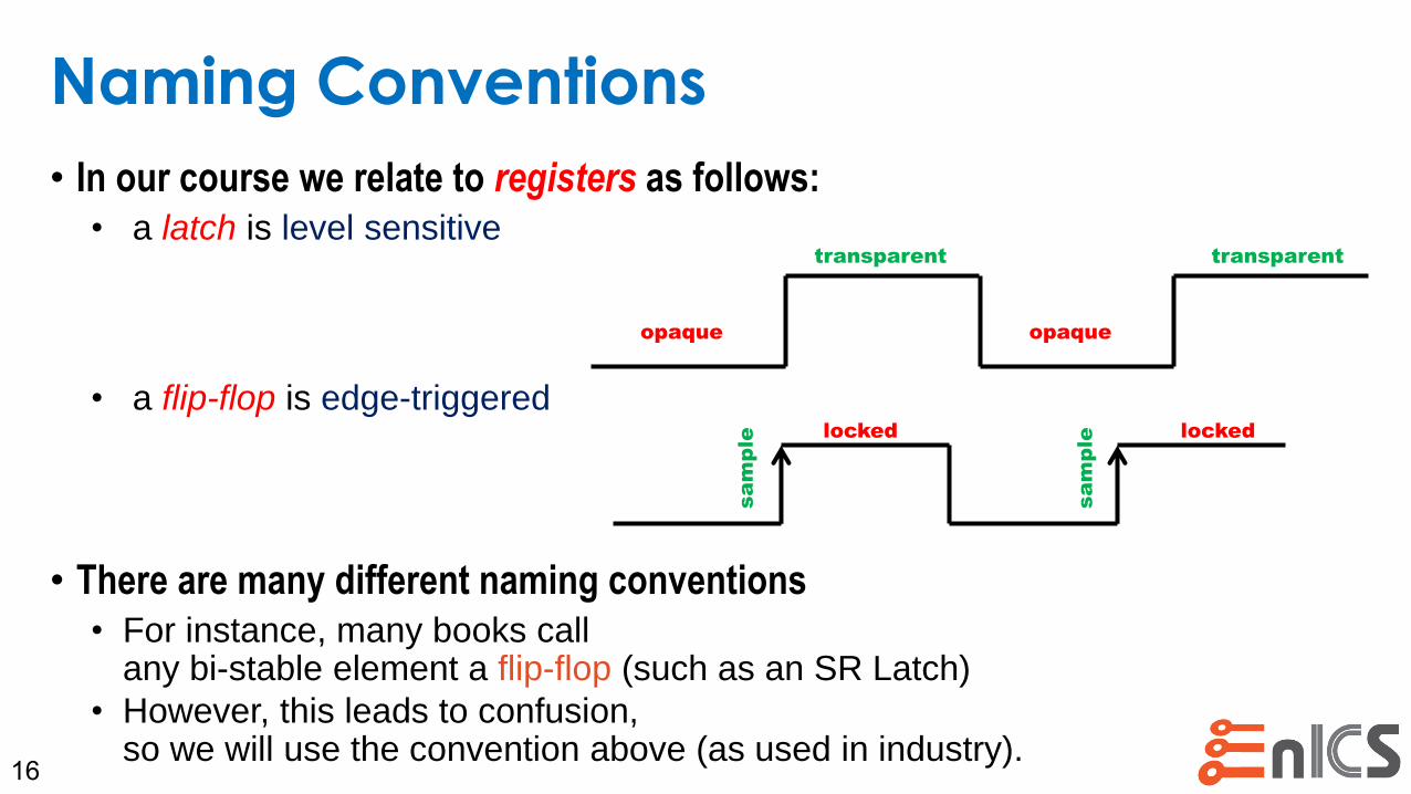
• In our course we relate to registers as follows:• a latch is level sensitive
• a flip-flop is edge-triggered
• There are many different naming conventions• For instance, many books call
any bi-stable element a flip-flop (such as an SR Latch)
• However, this leads to confusion, so we will use the convention above (as used in industry).
16
transparent
opaque
transparent
opaque
sa
mp
le
sa
mp
le
locked locked
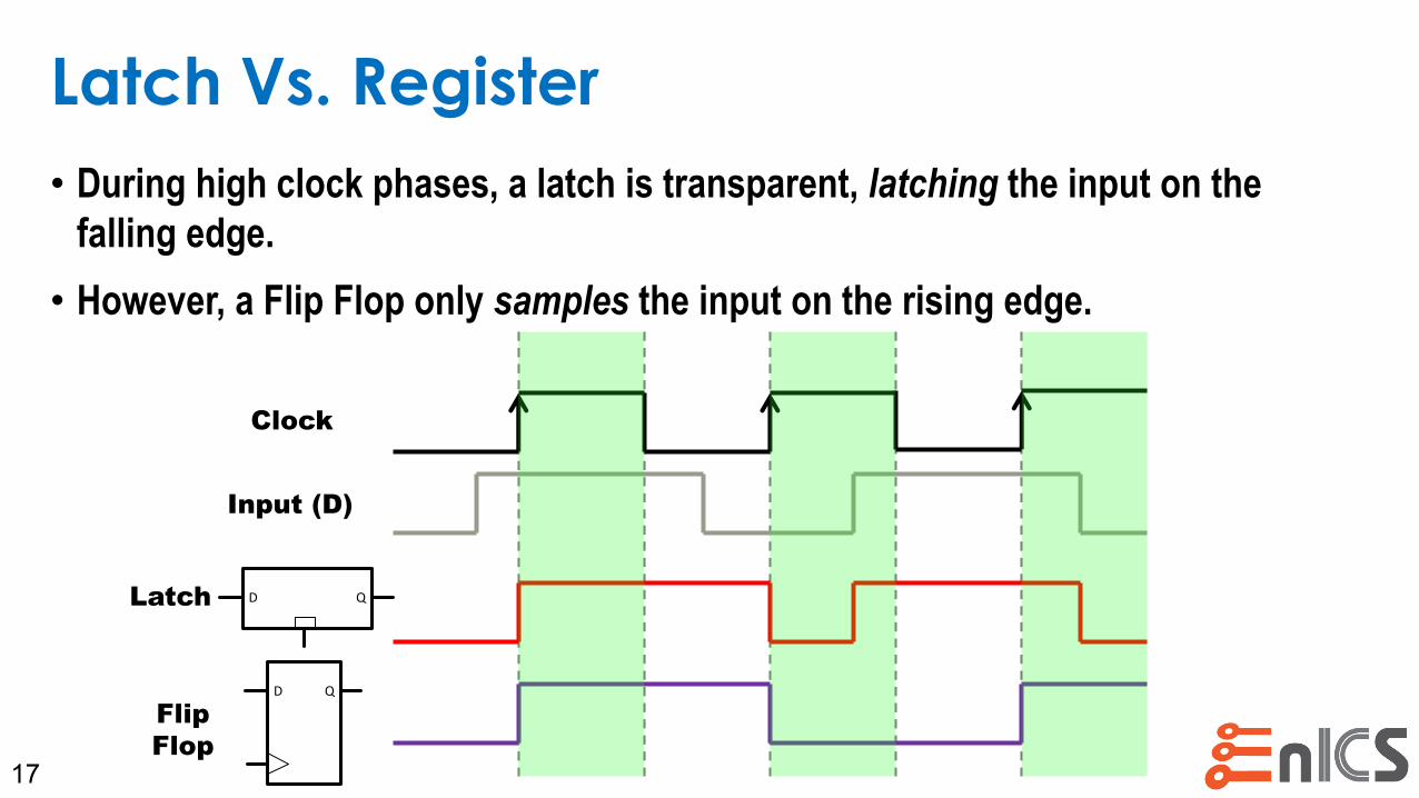
Latch Vs. Register
• During high clock phases, a latch is transparent, latching the input on the
falling edge.
• However, a Flip Flop only samples the input on the rising edge.
17
D QLatch
D Q
Flip
Flop
Clock
Input (D)
Latch Vs. Register
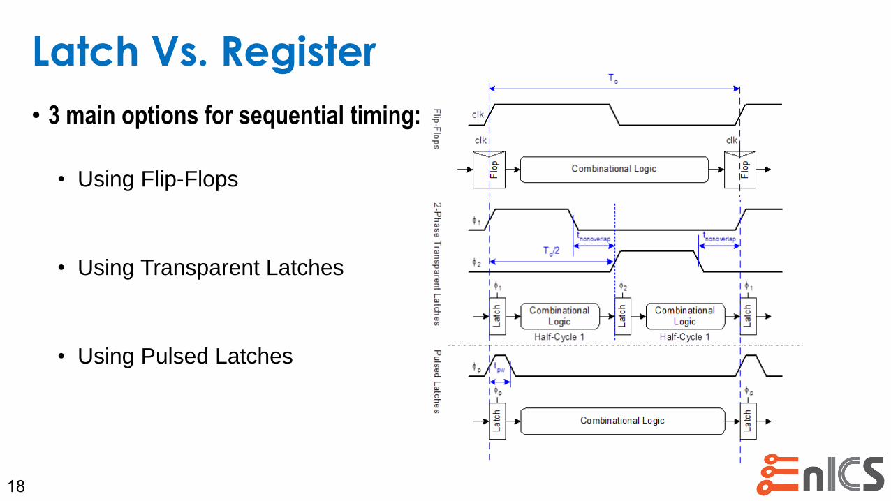
• 3 main options for sequential timing:
• Using Flip-Flops
• Using Transparent Latches
• Using Pulsed Latches
18
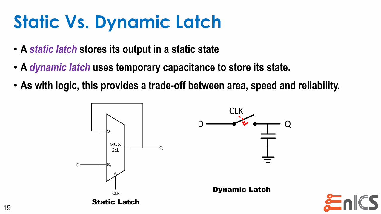
Static Vs. Dynamic Latch
• A static latch stores its output in a static state
• A dynamic latch uses temporary capacitance to store its state.
• As with logic, this provides a trade-off between area, speed and reliability.
19
D
CLK
Q
Dynamic Latch
MUX
2:1
S0
S1
S
CLK
D
Q
Static Latch

Static Vs. Dynamic Latch
• Some basic implementations of static and dynamic latches.
20
D
CLK
CLK
Q
Dynamic
CLK
CLK
CLK
D
Q
Static

Ratioed vs. Non-Ratioed Latch
• A static latch can be made by using a feedback inverter.
• The TG (with the driver before it)
must overcome the feedback
inverter to write into the latch.
• But it is usually more robust to create
a mux-based non-ratioed latch.
• At the expense of size.
21
CLK
CLK
CLK
D
Q
D
CLK
CLK
D
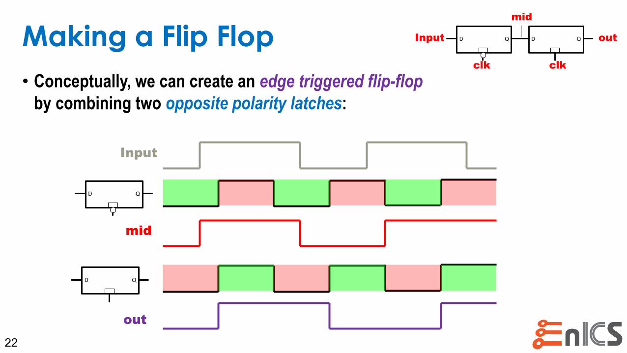
Making a Flip Flop
• Conceptually, we can create an edge triggered flip-flop
by combining two opposite polarity latches:
22
D Q
D Q
D Q D QInput
clk clk
out
mid
Input
mid
out
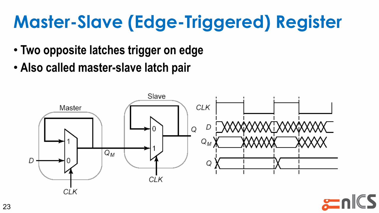
Master-Slave (Edge-Triggered) Register
• Two opposite latches trigger on edge
• Also called master-slave latch pair
23
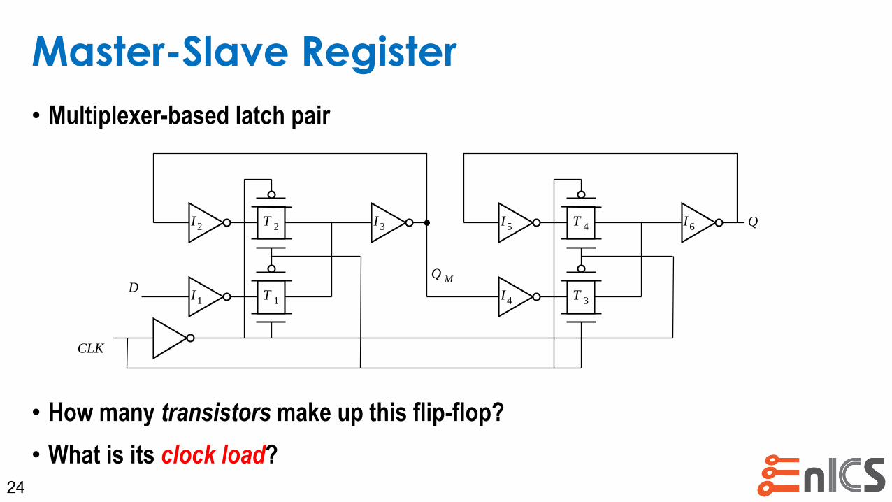
Master-Slave Register
• Multiplexer-based latch pair
• How many transistors make up this flip-flop?
• What is its clock load?24
Q M
Q
D
CLK
T 2I 2
T 1I 1
I 3 T 4I 5
T 3I 4
I 6

Resettable Flip Flops
25
Asynchronous Set/Reset Flip-Flop Synchronous Reset Flip-Flop
Timing Parameters of Sequential Elements
26

tcq – propagation delay
tsetup – setup time
thold – hold time
Timing Definitions
27
Register
CLK
D Q
t
CLK
t
D
t
QDATA
STABLE
DATA
STABLE
tsetup thold
tcq
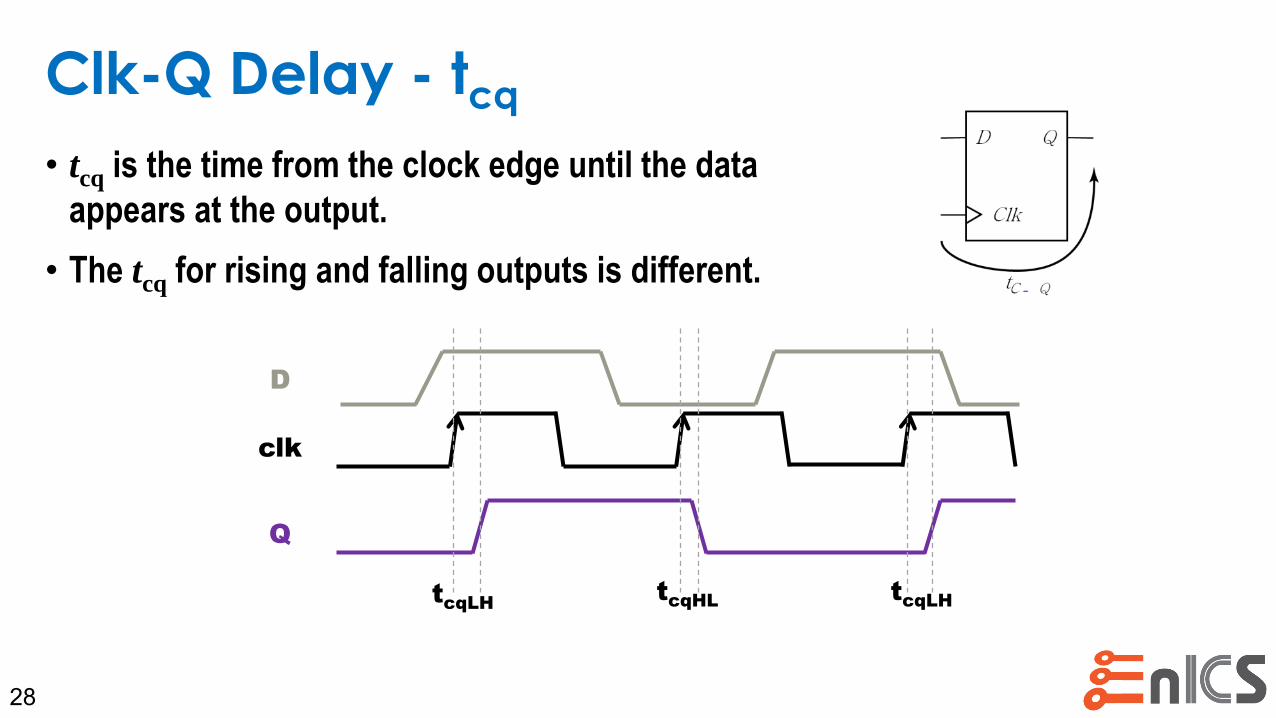
Clk-Q Delay - tcq
• tcq is the time from the clock edge until the data
appears at the output.
• The tcq for rising and falling outputs is different.
28
D
Q
clk
tcqLHtcqLHtcqHL

Mux based FF – tcq Calculation
• During low clock edge, data traverses slave
and “waits” for the clock at pass gate input.
• When clock rises, data has to go through pass gate and inverter.
29
QM
Q
D
CLK
T 2I2
T 1I1
I3 T 4I5
T 3I4
I6
3 6cqt T I

tcq – propagation delay
tsetup – setup time
thold – hold time
Timing Definitions
30
Register
CLK
D Q
t
CLK
t
D
t
QDATA
STABLE
DATA
STABLE
tsetup thold
tcq
BAD!Good!
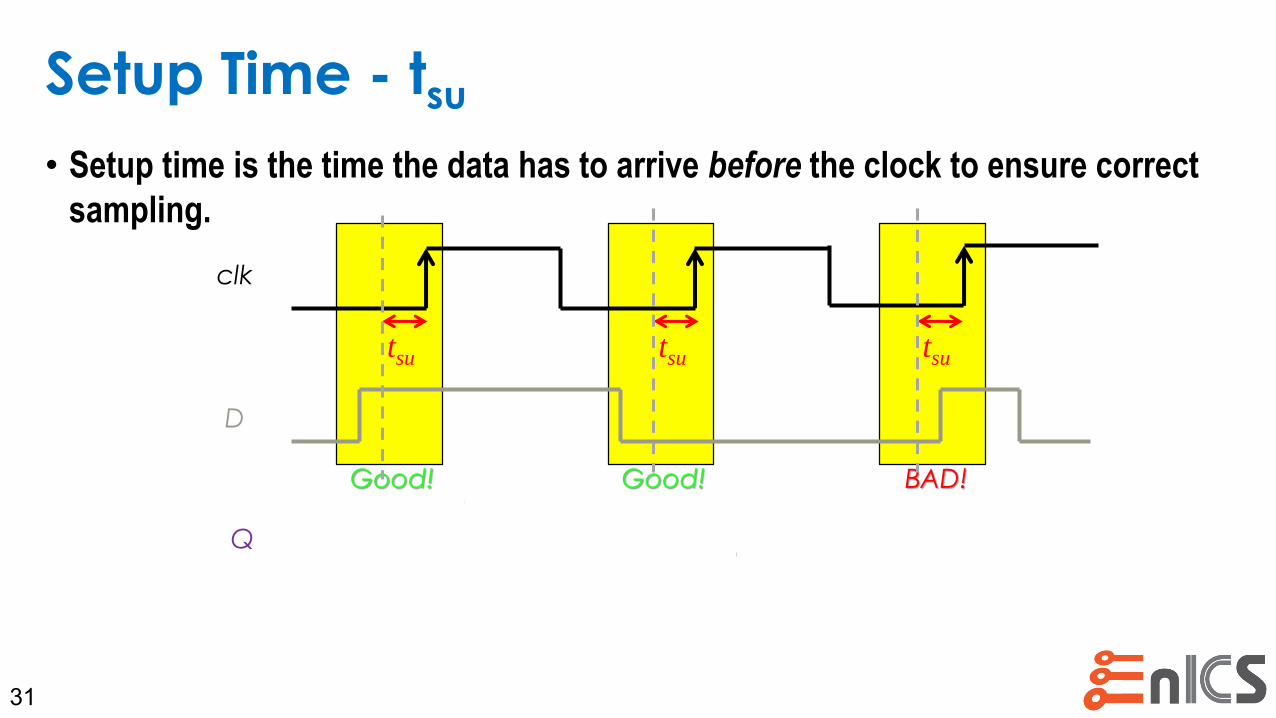
Setup Time - tsu
• Setup time is the time the data has to arrive before the clock to ensure correct
sampling.
31
D
clk
tsu tsu tsu
Q
Good!
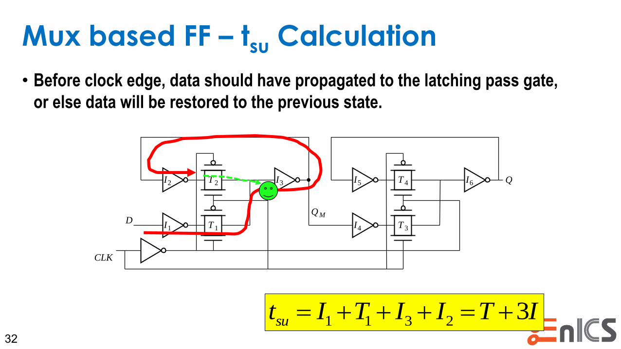
Mux based FF – tsu Calculation
• Before clock edge, data should have propagated to the latching pass gate,
or else data will be restored to the previous state.
32
QM
Q
D
CLK
T 2I2
T 1I1
I3 T 4I5
T 3I4
I6
1 1 3 2 3sut I T I I T I

Timing Analysis - Setup Time
• To obtain the setup time of the register while using SPICE, we
progressively skew the input with respect to the clock edge until the
circuit fails.
33

tcq – propagation delay
tsetup – setup time
thold – hold time
Timing Definitions
34
Register
CLK
D Q
t
CLK
t
D
t
QDATA
STABLE
DATA
STABLE
tsetup thold
tcq
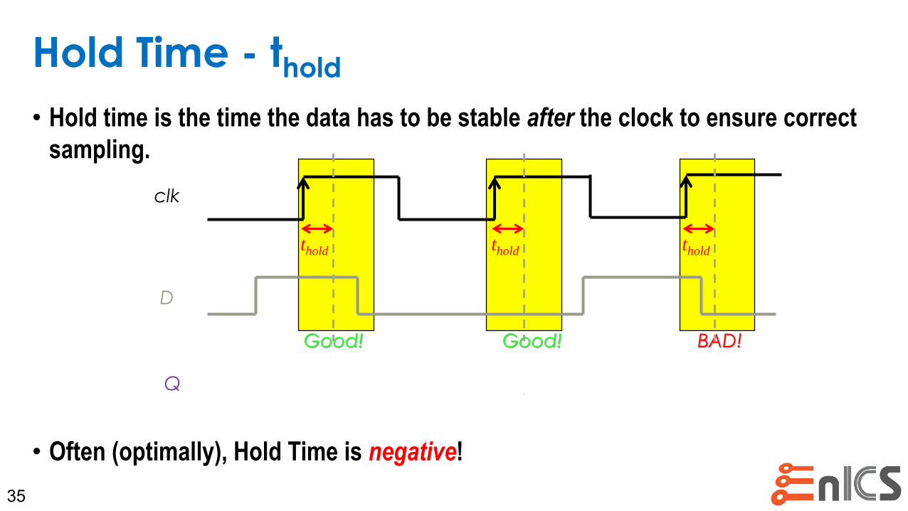
Hold Time - thold
• Hold time is the time the data has to be stable after the clock to ensure correct
sampling.
• Often (optimally), Hold Time is negative!
35
BAD!Good!
D
clk
thold
Q
Good!
thold thold

Mux based FF – thold Calculation
• When the clock rises, T1 closes, latching the data at the output of I1.
• Therefore, any changes made tpd(I1) before the clock will not traverse.
• The hold time is –tpd(I1)
36
QM
Q
D
CLK
T 2I2
T 1I1
I3 T 4I5
T 3I4
I6
1holdt I
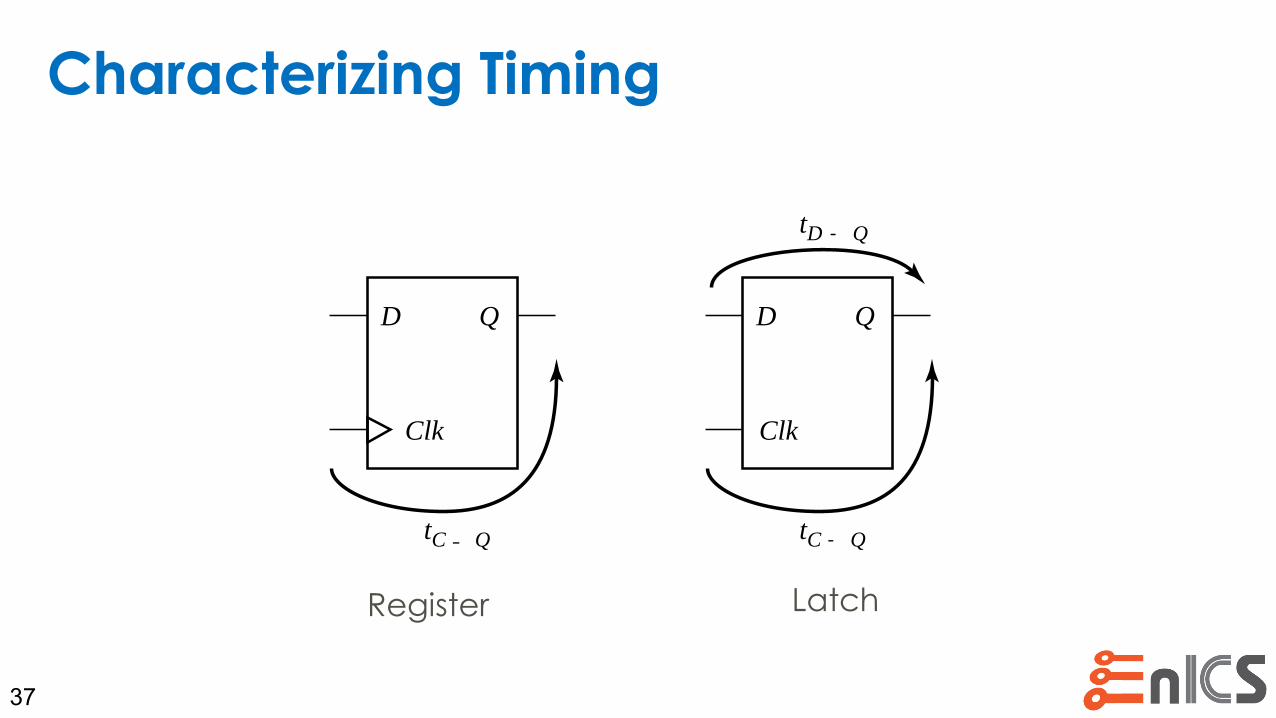
Characterizing Timing
37
Register Latch
Clk
D Q
tC - Q
Clk
D Q
tC - Q
tD - Q

Other Flip Flop Implementations
38

Problem – Clock Overlap
39
QM
Q
D
CLK
T 2I2
T 1I1
I3 T 4I5
T 3I4
I6
CLK
CLKb

C2MOS – clocked CMOS
• Insensitive to clock overlap.
40
CLK
CLKb
Low Phase Overlap High Phase Overlap
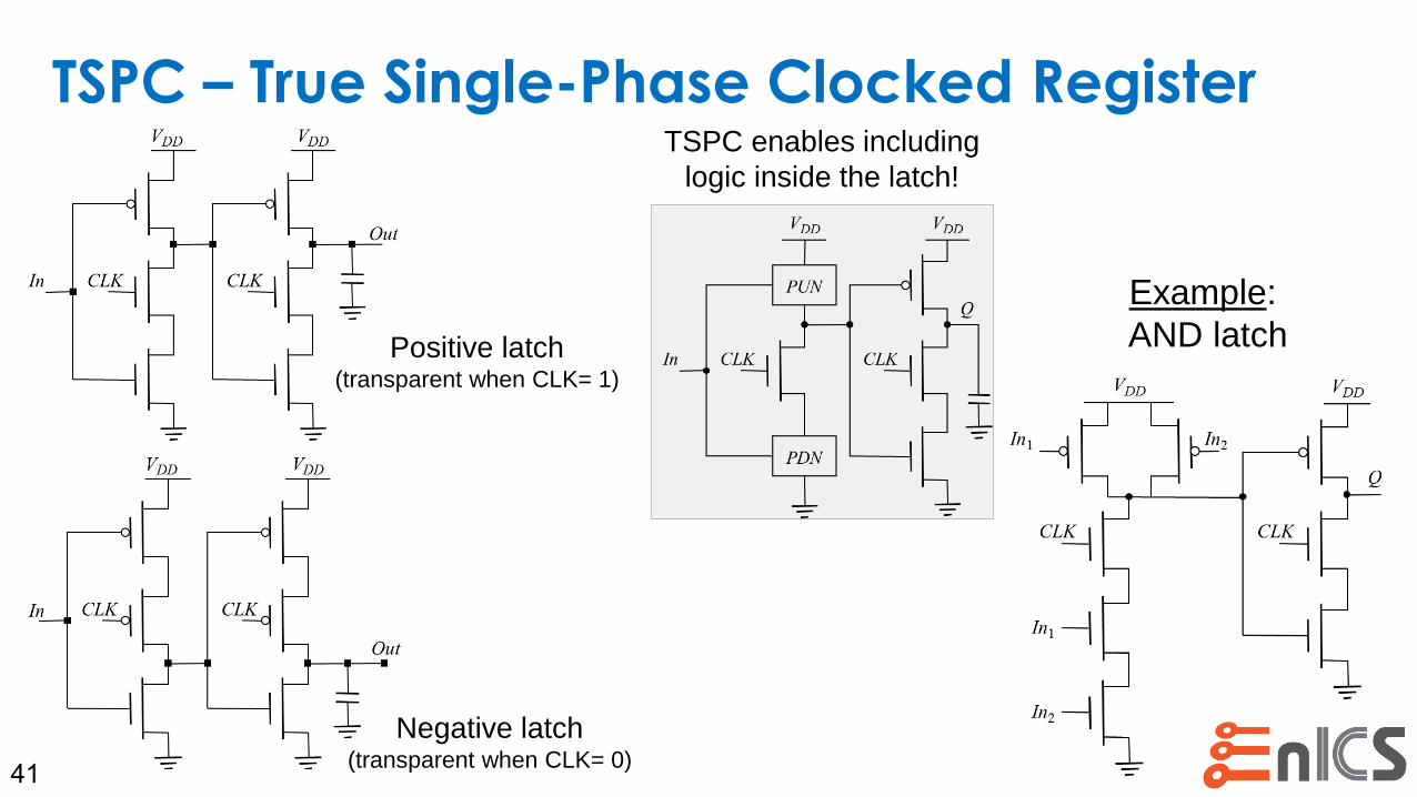
TSPC – True Single-Phase Clocked Register
41
Positive latch(transparent when CLK= 1)
Negative latch(transparent when CLK= 0)
Example:
AND latch
TSPC enables including
logic inside the latch!
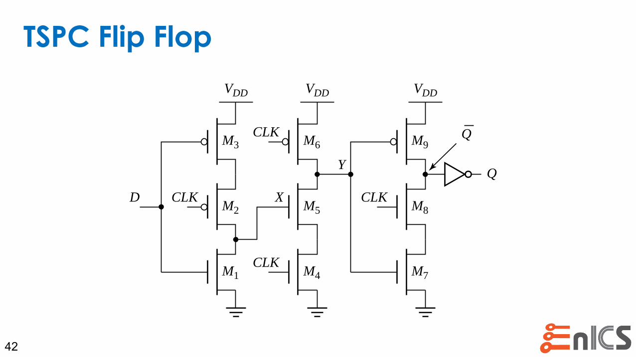
TSPC Flip Flop
42
CLK
CLK
D
VDD
M3
M2
M1
CLK
Y
VDD
Q
Q
M9
M8
M7
CLK
X
VDD
M6
M5
M4

Pulse-Triggered Latches
• Instead of a full set of master-slave latches
• We can emulate an edge with a short clock pulse:
43
Master-Slave Latches
D
Clk
Q D
Clk
Q
Clk
Data
L1 L2
Pulse-Triggered Latch
D
Clk
Q
Clk
DataL
Design a clock pulse with a “clock chopper”
Basic Timing Constraints
44

Synchronous Timing
45
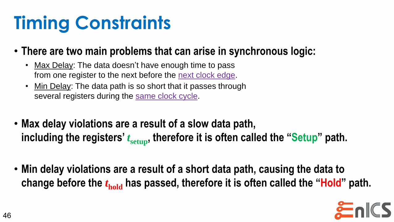
Timing Constraints
• There are two main problems that can arise in synchronous logic:• Max Delay: The data doesn’t have enough time to pass
from one register to the next before the next clock edge.
• Min Delay: The data path is so short that it passes through
several registers during the same clock cycle.
• Max delay violations are a result of a slow data path,
including the registers’ tsetup, therefore it is often called the “Setup” path.
• Min delay violations are a result of a short data path, causing the data to
change before the thold has passed, therefore it is often called the “Hold” path.
46

Setup (Max) Constraint• Let’s see what makes up our clock cycle:
• After the clock rises, it takes tcq for the data to propagate to point A.
• Then the data goes through the delay of the logic to get to point B.
• The data has to arrive at point B, tsetup before the next clock.
• In general, our timing path is a race:
• Between the Data Arrival, starting with the launching clock edge.
• And the Data Capture, one clock period later.
47
D
clk
A
tcq
D Q D QLogic
clk
A B
tsuB

Setup (Max) Constraint
48
cq logic setupT t t t
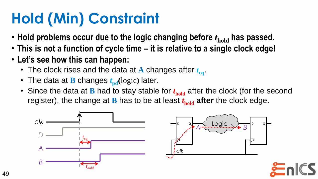
Hold (Min) Constraint• Hold problems occur due to the logic changing before thold has passed.
• This is not a function of cycle time – it is relative to a single clock edge!
• Let’s see how this can happen:• The clock rises and the data at A changes after tcq.
• The data at B changes tpd(logic) later.
• Since the data at B had to stay stable for thold after the clock (for the second
register), the change at B has to be at least thold after the clock edge.
49
D
clk
A
tcq
D Q D QLogic
clk
A B
thold
B
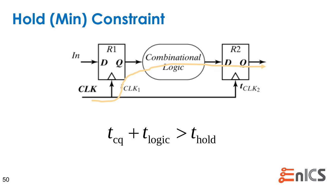
Hold (Min) Constraint
50
cq logic holdt t t

Summary
• For Setup constraints, the clock period has to be
longer than the data path delay:
• This sets our maximum frequency.
• If we have setup failures, we can always just
slow down the clock.
• For Hold constrains, the data path delay has to be
longer than the hold time:
• This is independent of clock period.
• If there is a hold failure, you can throw your chip away!
51
cq logic setupT t t t
cq logic holdt t t

Clock Nonidealities
• Clock skew• Spatial variation in temporally equivalent
clock edges; deterministic + random, tskew
• Clock jitter• Temporal variations in consecutive
edges of the clock signal;
modulation + random noise
• Cycle-to-cycle (short-term) tJit,S• Long term tJit,L
• Variation of the pulse width • Important for level sensitive clocking
52
Ref_Clock
DRVCLKt
Received Clock
skewt
RCVCLKt
T
jittjitt
skewt
Ref_Clock
Received Clock
T
skewtskewt
jitt jitt
RCV_CLKt
DRV_CLKt
Clock
uncertainty:
jitter+skew

Positive and Negative Skew
53
Positive skew
R1In Combinational
LogicD Q
tCLK1CLK
delay
tCLK2
R2
D QCombinational
Logic
tCLK3
R3
• • •D Q
delay
R1In
Negative skew
CombinationalLogic
D Q
tCLK1
delay
tCLK2
R2
D QCombinational
Logic
tCLK3
R3
• • •D Q
delay CLK

Setup (Max) Constraint
• The Launch path (still) consists of:
• tcq+tlogic+tsetup
• But if jitter makes the launch clock later,
we need to add it to the data path delay.
• The Capture path consists of:
• The clock period (T)
• Positive skew means the capture clock path is longer.
• If jitter makes the capture clock earlier, we need to subtract it.
• Our max constraint is:
• So we get:
54
launch cq logic setup jittert t t t t
capture skew jittert T t
capture launcht t
cq logic setup jitter skew2T t t t t
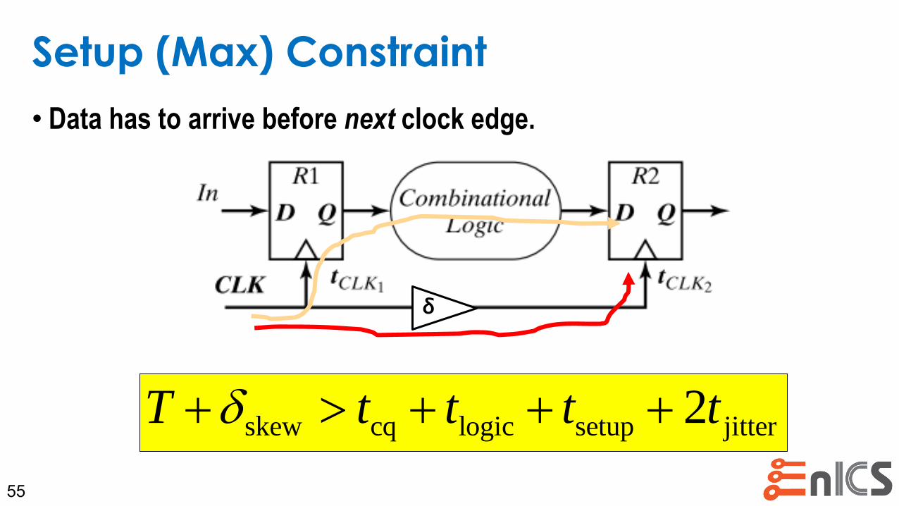
Setup (Max) Constraint
• Data has to arrive before next clock edge.
55
skew cq logic setup jitter2T t t t t
δ

Hold (Min) Constraint
• The Launch path (still) consists of:
• tcq+tlogic
• But if jitter makes the launch clock later,
we need to subtract it from the data path delay.
• The Capture path consists of:
• Skew that makes the clock edge arrive at the
capture register later than at the launch register.
• Actually, since it is a single clock edge, jitter should effect the capture clock the
same as the launch clock.
• But as a worst case, we will add it as spatial jitter.
• Our min constraint is:
• So we get:56
launch cq logic jittert t t t
capture skew jitter holdt t t
launch capturet t
cq logic skew hold jitter2t t t t

Hold (Min) Constraint
• Data has to arrive before after same clock edge has arrived at capture reg.
57
cq logic hold skew jitter2t t t t
δ

Adding in Variation
• Later in the course, we will discuss how variations in both fabrication
and operating conditions occur and are taken into account.
• For now, we should assume that certain fabrication characteristics
and operating conditions:• Can make our gates slower (i.e., high VT, high temperature, low voltage).
• Can make our gates faster (i.e., low VT, low temperature, high voltage).
• To assume worst-case conditions:• Calculate max-delay with the slowest possible transitions.
• Calculate min -delay with the fastest possible transitions.
58
Static Timing Analysis Example
59

STA Example
• We are given a synchronous network with:
• In addition:
60
150 , 50 , 100 , 0CQ SU hold jittert ps t ps t ps t
1 2100 , 50skew skewt ps t ps

STA Example
• We’ll find the setup
constraints for each path:
• So the critical path is Path 1 and the maximum frequency is 666MHz.61
1 1 1 ,max 1 2
1
Path 1:
150 1.2 50 100 1500 1.5 666
skew CQ p SUT t t t CL t
T p n p p p ns MHz
2 2 1 2 ,max 2 3
2
Path 2:
150 800 50 150 850 1.17
skew skew CQ p SUT t t t t CL t
T p p p p p GHz
3 2 3 ,max 3 1
3
Path 3: 0
150 700 50 50 950 1.05
skew CQ p SUT t t t CL t
T p p p p p GHz
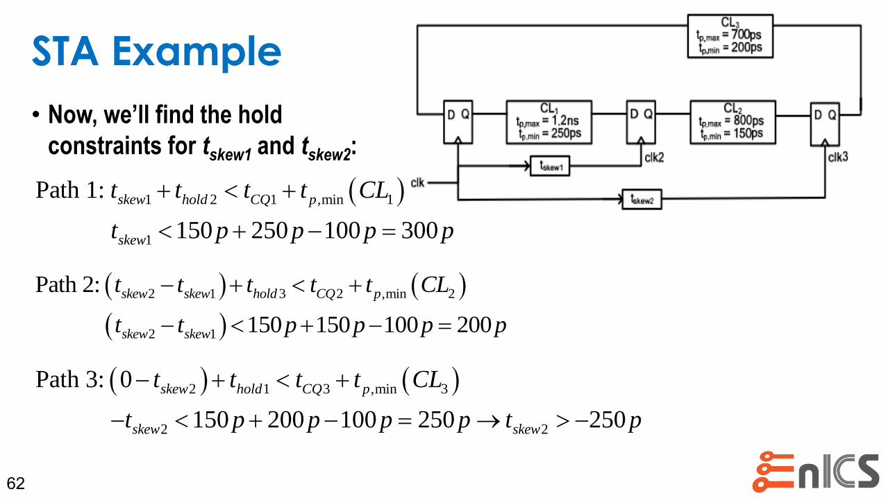
STA Example
• Now, we’ll find the hold
constraints for tskew1 and tskew2:
62
1 2 1 ,min 1
1
Path 1:
150 250 100 300
skew hold CQ p
skew
t t t t CL
t p p p p
2 1 3 2 ,min 2
2 1
Path 2:
150 150 100 200
skew skew hold CQ p
skew skew
t t t t t CL
t t p p p p
2 1 3 ,min 3
2 2
Path 3: 0
150 200 100 250 250
skew hold CQ p
skew skew
t t t t CL
t p p p p t p

STA Example
• If we could set tskew1 and tskew2,
could we use them to maximize
our frequency?
• If we could equally divide the delay of each path:
• So to get the max frequency, set all delays to 1.1nsec:
63
,max 1 2 33 ( ) 3
450 2.7 150 3.3 sec
total CQ p SUt t t CL CL CL t
p n p n
1 1
2 1 2
2 2
1.1 150 1.2 50 300 sec
1.1 150 800 50 200 sec
1.1 0 150 700 50 200 sec
skew skew
skew skew skew
skew skew
ns t p n p t p
ns t t p p p t p
ns t p p p t p

Further Reading
• J. Rabaey, “Digital Integrated Circuits” 2003, Chapter 7
• Weste, Harris “CMOS VLSI Design” Chapter 7
• E. Alon, Berkeley EE-141, Lectures 23,24 (Fall 2010) http://bwrc.eecs.berkeley.edu/classes/icdesign/ee141_f10/
• Berkeley CS-150, Lecture 4 http://inst.eecs.berkeley.edu/~cs150/
• Oklobdzija, Stojanovic, Markovic, Nedovic, “Digital System Clocking”
64