8xc151sa and 8xc151sb hardware description - keil · 8xc151sa and 8xc151sb hardware description...
TRANSCRIPT

June 1996
8XC151SA and 8XC151SBHardware Description
Order Number: 272832-001

Information in this document is provided in connection with Intel products. Intel assumes no liability whatsoev-er, including infringement of any patent or copyright, for sale and use of Intel products except as provided inIntel’s Terms and Conditions of Sale for such products.
Intel retains the right to make changes to these specifications at any time, without notice. MicrocomputerProducts may have minor variations to this specification known as errata.
*Other brands and names are the property of their respective owners.
²Since publication of documents referenced in this document, registration of the Pentium, OverDrive andiCOMP trademarks has been issued to Intel Corporation.
Contact your local Intel sales office or your distributor to obtain the latest specifications before placing yourproduct order.
Copies of documents which have an ordering number and are referenced in this document, or other Intelliterature, may be obtained from:
Intel CorporationP.O. Box 7641Mt. Prospect, IL 60056-7641
or call 1-800-879-4683
COPYRIGHT © INTEL CORPORATION, 1996

HARDWARE DESCRIPTION OF THE 8XC151SX
CONTENTS PAGE
1.0 INTRODUCTION ÀÀÀÀÀÀÀÀÀÀÀÀÀÀÀÀÀÀÀÀÀÀÀ 1
2.0 MEMORY ORGANIZATION ÀÀÀÀÀÀÀÀÀÀÀÀ 2
2.1 Program Memory ÀÀÀÀÀÀÀÀÀÀÀÀÀÀÀÀÀÀÀÀ 2
2.2 Data Memory ÀÀÀÀÀÀÀÀÀÀÀÀÀÀÀÀÀÀÀÀÀÀÀÀ 2
3.0 SPECIAL FUNCTIONREGISTERS ÀÀÀÀÀÀÀÀÀÀÀÀÀÀÀÀÀÀÀÀÀÀÀÀÀÀÀÀÀ 4
4.0 PORT STRUCTURES ANDOPERATION ÀÀÀÀÀÀÀÀÀÀÀÀÀÀÀÀÀÀÀÀÀÀÀÀÀÀÀ 10
4.1 I/O Configurations ÀÀÀÀÀÀÀÀÀÀÀÀÀÀÀÀÀÀ 10
4.2 Port 1 and Port 3 ÀÀÀÀÀÀÀÀÀÀÀÀÀÀÀÀÀÀÀ 10
4.3 Port 0 and Port 2 ÀÀÀÀÀÀÀÀÀÀÀÀÀÀÀÀÀÀÀ 10
4.4 Read-Modify-Write Instructions ÀÀÀÀÀ 13
4.5 Quasi-Bidirectional PortOperation ÀÀÀÀÀÀÀÀÀÀÀÀÀÀÀÀÀÀÀÀÀÀÀÀÀÀÀÀ 13
4.6 Port Loading ÀÀÀÀÀÀÀÀÀÀÀÀÀÀÀÀÀÀÀÀÀÀÀ 14
4.7 Accessing External Memory ÀÀÀÀÀÀÀÀ 15
4.7.1 Bus Cycle Definition ÀÀÀÀÀÀÀÀÀÀÀ 17
4.7.2 External Bus Cycles with WaitStates ÀÀÀÀÀÀÀÀÀÀÀÀÀÀÀÀÀÀÀÀÀÀÀÀÀÀÀÀ 21
4.7.3 Port 0 and Port 2 for States inNon-Page and Page Mode ÀÀÀÀÀÀÀÀ 22
5.0 TIMERS/COUNTERS ÀÀÀÀÀÀÀÀÀÀÀÀÀÀÀÀÀ 23
5.1 TIMER 0 AND TIMER 1 ÀÀÀÀÀÀÀÀÀÀÀÀÀ 23
5.2 TIMER 2 ÀÀÀÀÀÀÀÀÀÀÀÀÀÀÀÀÀÀÀÀÀÀÀÀÀÀÀ 26
6.0 PROGRAMMABLE COUNTERARRAY ÀÀÀÀÀÀÀÀÀÀÀÀÀÀÀÀÀÀÀÀÀÀÀÀÀÀÀÀÀÀÀÀÀ 30
6.1 PCA 16-Bit Timer/Counter ÀÀÀÀÀÀÀÀÀÀ 32
6.2 Capture/Compare Modules ÀÀÀÀÀÀÀÀÀ 34
6.3 16-Bit Capture Mode ÀÀÀÀÀÀÀÀÀÀÀÀÀÀÀ 37
6.4 16-Bit Software Timer Mode ÀÀÀÀÀÀÀÀ 37
6.5 High Speed Output Mode ÀÀÀÀÀÀÀÀÀÀÀ 38
6.6 Watchdog Timer Mode ÀÀÀÀÀÀÀÀÀÀÀÀÀ 38
6.7 Pulse Width Modulator Mode ÀÀÀÀÀÀÀ 39
CONTENTS PAGE
7.0 SERIAL INTERFACE ÀÀÀÀÀÀÀÀÀÀÀÀÀÀÀÀÀ 41
7.1 Framing Error Detection ÀÀÀÀÀÀÀÀÀÀÀÀ 42
7.2 Multiprocessor Communications ÀÀÀÀ 42
7.3 Automatic Address Recognition ÀÀÀÀÀ 42
7.4 Baud Rates ÀÀÀÀÀÀÀÀÀÀÀÀÀÀÀÀÀÀÀÀÀÀÀÀ 44
7.5 Using Timer 1 to Generate BaudRates ÀÀÀÀÀÀÀÀÀÀÀÀÀÀÀÀÀÀÀÀÀÀÀÀÀÀÀÀÀÀÀÀ 44
7.6 Using Timer 2 to Generate BaudRates ÀÀÀÀÀÀÀÀÀÀÀÀÀÀÀÀÀÀÀÀÀÀÀÀÀÀÀÀÀÀÀÀ 45
8.0 WATCHDOG TIMER ÀÀÀÀÀÀÀÀÀÀÀÀÀÀÀÀÀÀ 46
8.1 Using the WDT ÀÀÀÀÀÀÀÀÀÀÀÀÀÀÀÀÀÀÀÀÀ 46
8.2 WDT during Idle Mode andPowerdown ÀÀÀÀÀÀÀÀÀÀÀÀÀÀÀÀÀÀÀÀÀÀÀÀÀÀ 46
9.0 INTERRUPTS ÀÀÀÀÀÀÀÀÀÀÀÀÀÀÀÀÀÀÀÀÀÀÀÀÀ 47
9.1 External Interrupts ÀÀÀÀÀÀÀÀÀÀÀÀÀÀÀÀÀÀ 47
9.2 Timer Interrupts ÀÀÀÀÀÀÀÀÀÀÀÀÀÀÀÀÀÀÀÀ 49
9.3 PCA Interrupt ÀÀÀÀÀÀÀÀÀÀÀÀÀÀÀÀÀÀÀÀÀÀÀ 50
9.4 Serial Port Interrupt ÀÀÀÀÀÀÀÀÀÀÀÀÀÀÀÀÀ 50
9.5 Interrupt Enable ÀÀÀÀÀÀÀÀÀÀÀÀÀÀÀÀÀÀÀÀ 50
9.6 Interrupt Priorities ÀÀÀÀÀÀÀÀÀÀÀÀÀÀÀÀÀÀ 51
9.7 Interrupt Processing ÀÀÀÀÀÀÀÀÀÀÀÀÀÀÀÀ 54
9.7.1 Minimum Fixed InterruptTime ÀÀÀÀÀÀÀÀÀÀÀÀÀÀÀÀÀÀÀÀÀÀÀÀÀÀÀÀÀÀ 55
9.7.2 Variable InterruptParameter ÀÀÀÀÀÀÀÀÀÀÀÀÀÀÀÀÀÀÀÀÀÀÀÀ 55
9.7.3 Response Time Variables ÀÀÀÀÀÀ 55
9.7.4 Computation of Worst-CaseLatency With Variables ÀÀÀÀÀÀÀÀÀÀÀÀ 56
9.7.5 Blocking Conditions ÀÀÀÀÀÀÀÀÀÀÀ 57
9.7.6 Interrupt Vector Cycle ÀÀÀÀÀÀÀÀÀ 57
9.7.7 ISRs in Process ÀÀÀÀÀÀÀÀÀÀÀÀÀÀÀ 58
iii
CONTENTS PAGE
10.0 RESET ÀÀÀÀÀÀÀÀÀÀÀÀÀÀÀÀÀÀÀÀÀÀÀÀÀÀÀÀÀÀ 58
10.1 Externally Initiated Resets ÀÀÀÀÀÀÀÀÀ 58
10.2 WDT Initiated Resets ÀÀÀÀÀÀÀÀÀÀÀÀÀÀ 59
10.3 Reset Operation ÀÀÀÀÀÀÀÀÀÀÀÀÀÀÀÀÀÀ 59
10.4 Power-on Reset ÀÀÀÀÀÀÀÀÀÀÀÀÀÀÀÀÀÀÀ 59
11.0 POWER-SAVING MODES OFOPERATION ÀÀÀÀÀÀÀÀÀÀÀÀÀÀÀÀÀÀÀÀÀÀÀÀÀÀÀ 60
11.1 Idle Mode ÀÀÀÀÀÀÀÀÀÀÀÀÀÀÀÀÀÀÀÀÀÀÀÀÀ 60
CONTENTS PAGE
12.0 PROGRAMMING AND VERIFYINGNONVOLATILE MEMORY ÀÀÀÀÀÀÀÀÀÀÀÀÀÀ 62
12.1 Programming and VerifyingModes ÀÀÀÀÀÀÀÀÀÀÀÀÀÀÀÀÀÀÀÀÀÀÀÀÀÀÀÀÀÀÀ 62
12.2 Lock Bit System ÀÀÀÀÀÀÀÀÀÀÀÀÀÀÀÀÀÀÀ 64
12.3 Encryption Array ÀÀÀÀÀÀÀÀÀÀÀÀÀÀÀÀÀÀ 64
12.4 Signature Bytes ÀÀÀÀÀÀÀÀÀÀÀÀÀÀÀÀÀÀÀ 64
13.0 ON-CIRCUIT EMULATION (ONCE)MODE ÀÀÀÀÀÀÀÀÀÀÀÀÀÀÀÀÀÀÀÀÀÀÀÀÀÀÀÀÀÀÀÀÀÀ 65
14.0 ON-CHIP OSCILLATOR ÀÀÀÀÀÀÀÀÀÀÀÀÀ 66
15.0 INSTRUCTION SETREFERENCE ÀÀÀÀÀÀÀÀÀÀÀÀÀÀÀÀÀÀÀÀÀÀÀÀÀÀÀ 68
iv
CONTENTS PAGE
Figure 1. 8XC151SA/SB Functional Block Diagram ÀÀÀÀÀÀÀÀÀÀÀÀÀÀÀÀÀÀÀÀÀÀÀÀÀÀÀÀÀÀÀÀÀÀÀÀÀÀÀÀÀ 3
Figure 2. Internal Data Memory ÀÀÀÀÀÀÀÀÀÀÀÀÀÀÀÀÀÀÀÀÀÀÀÀÀÀÀÀÀÀÀÀÀÀÀÀÀÀÀÀÀÀÀÀÀÀÀÀÀÀÀÀÀÀÀÀÀÀÀÀÀ 3
Figure 3. Port 1 and Port 3 Structure ÀÀÀÀÀÀÀÀÀÀÀÀÀÀÀÀÀÀÀÀÀÀÀÀÀÀÀÀÀÀÀÀÀÀÀÀÀÀÀÀÀÀÀÀÀÀÀÀÀÀÀÀÀÀÀ 11
Figure 4. Port 0 Structure ÀÀÀÀÀÀÀÀÀÀÀÀÀÀÀÀÀÀÀÀÀÀÀÀÀÀÀÀÀÀÀÀÀÀÀÀÀÀÀÀÀÀÀÀÀÀÀÀÀÀÀÀÀÀÀÀÀÀÀÀÀÀÀÀÀÀ 11
Figure 5. Port 2 Structure ÀÀÀÀÀÀÀÀÀÀÀÀÀÀÀÀÀÀÀÀÀÀÀÀÀÀÀÀÀÀÀÀÀÀÀÀÀÀÀÀÀÀÀÀÀÀÀÀÀÀÀÀÀÀÀÀÀÀÀÀÀÀÀÀÀÀ 12
Figure 6. Internal Pullup Configurations ÀÀÀÀÀÀÀÀÀÀÀÀÀÀÀÀÀÀÀÀÀÀÀÀÀÀÀÀÀÀÀÀÀÀÀÀÀÀÀÀÀÀÀÀÀÀÀÀÀÀÀÀ 14
Figure 7. Bus Structure in Nonpage Mode and Page Mode ÀÀÀÀÀÀÀÀÀÀÀÀÀÀÀÀÀÀÀÀÀÀÀÀÀÀÀÀÀÀÀÀÀ 15
Figure 8. External Bus Cycle: Code Fetch, Nonpage Mode ÀÀÀÀÀÀÀÀÀÀÀÀÀÀÀÀÀÀÀÀÀÀÀÀÀÀÀÀÀÀÀÀÀ 17
Figure 9. External Bus Cycle: Data Read, Nonpage Mode ÀÀÀÀÀÀÀÀÀÀÀÀÀÀÀÀÀÀÀÀÀÀÀÀÀÀÀÀÀÀÀÀÀÀ 18
Figure 10. External Bus Cycle: Data Write, Nonpage Mode ÀÀÀÀÀÀÀÀÀÀÀÀÀÀÀÀÀÀÀÀÀÀÀÀÀÀÀÀÀÀÀÀÀ 18
Figure 11. External Bus Cycle: Code Fetch, Page Mode ÀÀÀÀÀÀÀÀÀÀÀÀÀÀÀÀÀÀÀÀÀÀÀÀÀÀÀÀÀÀÀÀÀÀÀÀ 20
Figure 12. External Bus Cycle: Data Read, Page Mode ÀÀÀÀÀÀÀÀÀÀÀÀÀÀÀÀÀÀÀÀÀÀÀÀÀÀÀÀÀÀÀÀÀÀÀÀÀ 20
Figure 13. External Bus Cycle: Data Write, Page Mode ÀÀÀÀÀÀÀÀÀÀÀÀÀÀÀÀÀÀÀÀÀÀÀÀÀÀÀÀÀÀÀÀÀÀÀÀÀ 21
Figure 14. External Bus Cycle: Data Write with One WRÝ Wait State (Nonpage Mode) ÀÀÀÀÀÀ 21
Figure 15. External Bus Cycle: Code Fetch with One ALE Wait State (Nonpage Mode) ÀÀÀÀÀÀ 22
Figure 16. Timer/Counter 0 or 1 in Mode 0: 13-Bit Counter ÀÀÀÀÀÀÀÀÀÀÀÀÀÀÀÀÀÀÀÀÀÀÀÀÀÀÀÀÀÀÀÀÀ 24
Figure 17. Timer/Counter 0 or 1 in Mode 1: 16-Bit Counter ÀÀÀÀÀÀÀÀÀÀÀÀÀÀÀÀÀÀÀÀÀÀÀÀÀÀÀÀÀÀÀÀÀ 25
Figure 18. Timer/Counter 1 Mode 2: 8-Bit Auto-Reload ÀÀÀÀÀÀÀÀÀÀÀÀÀÀÀÀÀÀÀÀÀÀÀÀÀÀÀÀÀÀÀÀÀÀÀÀ 26
Figure 19. Timer/Counter 0 Mode 3: Two 8-Bit Counters ÀÀÀÀÀÀÀÀÀÀÀÀÀÀÀÀÀÀÀÀÀÀÀÀÀÀÀÀÀÀÀÀÀÀÀ 26
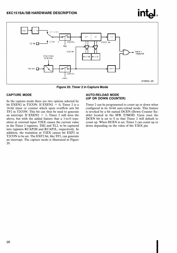
Figure 20. Timer 2 in Capture Mode ÀÀÀÀÀÀÀÀÀÀÀÀÀÀÀÀÀÀÀÀÀÀÀÀÀÀÀÀÀÀÀÀÀÀÀÀÀÀÀÀÀÀÀÀÀÀÀÀÀÀÀÀÀÀÀÀ 28
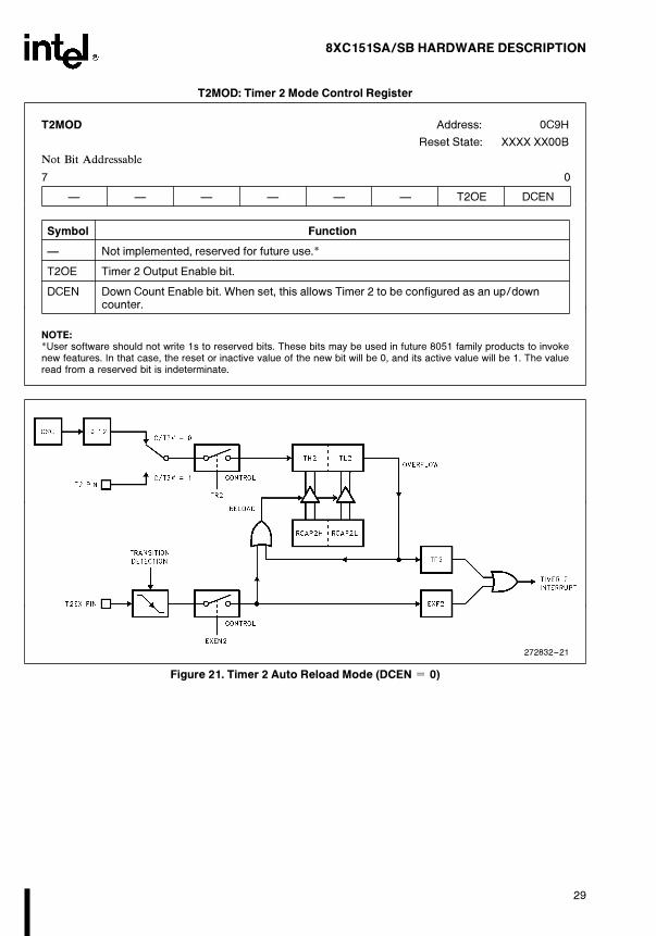
Figure 21. Timer 2 Auto Reload Mode (DCEN e 0) ÀÀÀÀÀÀÀÀÀÀÀÀÀÀÀÀÀÀÀÀÀÀÀÀÀÀÀÀÀÀÀÀÀÀÀÀÀÀÀÀ 29
Figure 22. Timer 2 Auto Reload Mode (DCEN e 1) ÀÀÀÀÀÀÀÀÀÀÀÀÀÀÀÀÀÀÀÀÀÀÀÀÀÀÀÀÀÀÀÀÀÀÀÀÀÀÀÀ 31
Figure 23. Timer 2 in Clock-Out Mode ÀÀÀÀÀÀÀÀÀÀÀÀÀÀÀÀÀÀÀÀÀÀÀÀÀÀÀÀÀÀÀÀÀÀÀÀÀÀÀÀÀÀÀÀÀÀÀÀÀÀÀÀÀ 31
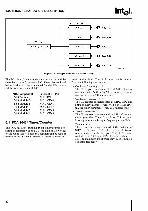
Figure 24. Programmable Counter Array ÀÀÀÀÀÀÀÀÀÀÀÀÀÀÀÀÀÀÀÀÀÀÀÀÀÀÀÀÀÀÀÀÀÀÀÀÀÀÀÀÀÀÀÀÀÀÀÀÀÀÀ 32
Figure 25. PCA Timer/Counter ÀÀÀÀÀÀÀÀÀÀÀÀÀÀÀÀÀÀÀÀÀÀÀÀÀÀÀÀÀÀÀÀÀÀÀÀÀÀÀÀÀÀÀÀÀÀÀÀÀÀÀÀÀÀÀÀÀÀÀÀ 33
Figure 26. PCA 16-Bit Capture Mode ÀÀÀÀÀÀÀÀÀÀÀÀÀÀÀÀÀÀÀÀÀÀÀÀÀÀÀÀÀÀÀÀÀÀÀÀÀÀÀÀÀÀÀÀÀÀÀÀÀÀÀÀÀÀ 37
Figure 27. PCA 16-Bit Comparator Mode: Software Timer and High Speed Output ÀÀÀÀÀÀÀÀÀÀ 39
Figure 28. Watchdog Timer Mode ÀÀÀÀÀÀÀÀÀÀÀÀÀÀÀÀÀÀÀÀÀÀÀÀÀÀÀÀÀÀÀÀÀÀÀÀÀÀÀÀÀÀÀÀÀÀÀÀÀÀÀÀÀÀÀÀÀ 40
Figure 29. PCA 8-Bit PWM Mode ÀÀÀÀÀÀÀÀÀÀÀÀÀÀÀÀÀÀÀÀÀÀÀÀÀÀÀÀÀÀÀÀÀÀÀÀÀÀÀÀÀÀÀÀÀÀÀÀÀÀÀÀÀÀÀÀÀÀ 40
Figure 30. CCAPnH Varies Duty Cycle ÀÀÀÀÀÀÀÀÀÀÀÀÀÀÀÀÀÀÀÀÀÀÀÀÀÀÀÀÀÀÀÀÀÀÀÀÀÀÀÀÀÀÀÀÀÀÀÀÀÀÀÀÀ 41
Figure 31. Data Frame: Modes 1, 2 and 3 ÀÀÀÀÀÀÀÀÀÀÀÀÀÀÀÀÀÀÀÀÀÀÀÀÀÀÀÀÀÀÀÀÀÀÀÀÀÀÀÀÀÀÀÀÀÀÀÀÀÀ 41
Figure 32. Timer 2 in Baud Rate Generator Mode ÀÀÀÀÀÀÀÀÀÀÀÀÀÀÀÀÀÀÀÀÀÀÀÀÀÀÀÀÀÀÀÀÀÀÀÀÀÀÀÀÀÀ 45
Figure 33. Interrupt Control System ÀÀÀÀÀÀÀÀÀÀÀÀÀÀÀÀÀÀÀÀÀÀÀÀÀÀÀÀÀÀÀÀÀÀÀÀÀÀÀÀÀÀÀÀÀÀÀÀÀÀÀÀÀÀÀÀ 48
Figure 34. The Interrupt Process ÀÀÀÀÀÀÀÀÀÀÀÀÀÀÀÀÀÀÀÀÀÀÀÀÀÀÀÀÀÀÀÀÀÀÀÀÀÀÀÀÀÀÀÀÀÀÀÀÀÀÀÀÀÀÀÀÀÀÀ 54
Figure 35. Response Time Example Ý1 ÀÀÀÀÀÀÀÀÀÀÀÀÀÀÀÀÀÀÀÀÀÀÀÀÀÀÀÀÀÀÀÀÀÀÀÀÀÀÀÀÀÀÀÀÀÀÀÀÀÀÀ 56
Figure 36. Response Time Example Ý2 ÀÀÀÀÀÀÀÀÀÀÀÀÀÀÀÀÀÀÀÀÀÀÀÀÀÀÀÀÀÀÀÀÀÀÀÀÀÀÀÀÀÀÀÀÀÀÀÀÀÀÀ 56
v
CONTENTS PAGE
Figure 37. External Clock Drive Waveforms ÀÀÀÀÀÀÀÀÀÀÀÀÀÀÀÀÀÀÀÀÀÀÀÀÀÀÀÀÀÀÀÀÀÀÀÀÀÀÀÀÀÀÀÀÀÀÀÀ 58
Figure 38. Power on Reset Circuitry ÀÀÀÀÀÀÀÀÀÀÀÀÀÀÀÀÀÀÀÀÀÀÀÀÀÀÀÀÀÀÀÀÀÀÀÀÀÀÀÀÀÀÀÀÀÀÀÀÀÀÀÀÀÀÀÀ 59
Figure 39. Reset Timing Sequence ÀÀÀÀÀÀÀÀÀÀÀÀÀÀÀÀÀÀÀÀÀÀÀÀÀÀÀÀÀÀÀÀÀÀÀÀÀÀÀÀÀÀÀÀÀÀÀÀÀÀÀÀÀÀÀÀ 60
Figure 40. Idle and Power Down Hardware ÀÀÀÀÀÀÀÀÀÀÀÀÀÀÀÀÀÀÀÀÀÀÀÀÀÀÀÀÀÀÀÀÀÀÀÀÀÀÀÀÀÀÀÀÀÀÀÀÀ 61
Figure 41. Setup for Programming and Verifying Nonvolatile Memory ÀÀÀÀÀÀÀÀÀÀÀÀÀÀÀÀÀÀÀÀÀÀÀ 62
Figure 42. CHMOS On-chip Oscillator ÀÀÀÀÀÀÀÀÀÀÀÀÀÀÀÀÀÀÀÀÀÀÀÀÀÀÀÀÀÀÀÀÀÀÀÀÀÀÀÀÀÀÀÀÀÀÀÀÀÀÀÀÀ 66
Figure 43. External Clock Connection ÀÀÀÀÀÀÀÀÀÀÀÀÀÀÀÀÀÀÀÀÀÀÀÀÀÀÀÀÀÀÀÀÀÀÀÀÀÀÀÀÀÀÀÀÀÀÀÀÀÀÀÀÀÀ 67
Figure 44. External Clock Drive Waveforms ÀÀÀÀÀÀÀÀÀÀÀÀÀÀÀÀÀÀÀÀÀÀÀÀÀÀÀÀÀÀÀÀÀÀÀÀÀÀÀÀÀÀÀÀÀÀÀÀ 68
vi

CONTENTS PAGE
Table 1. 8XC151 Family of Microcontrollers ÀÀÀÀÀÀÀÀÀÀÀÀÀÀÀÀÀÀÀÀÀÀÀÀÀÀÀÀÀÀÀÀÀÀÀÀÀÀÀÀÀÀÀÀÀÀÀÀÀ 2
Table 2. 8XC151SA/SB Map and Reset Values ÀÀÀÀÀÀÀÀÀÀÀÀÀÀÀÀÀÀÀÀÀÀÀÀÀÀÀÀÀÀÀÀÀÀÀÀÀÀÀÀÀÀÀÀÀ 4
Table 3. Core SFRs ÀÀÀÀÀÀÀÀÀÀÀÀÀÀÀÀÀÀÀÀÀÀÀÀÀÀÀÀÀÀÀÀÀÀÀÀÀÀÀÀÀÀÀÀÀÀÀÀÀÀÀÀÀÀÀÀÀÀÀÀÀÀÀÀÀÀÀÀÀÀÀÀ 5
Table 4. I/O Port SFRs ÀÀÀÀÀÀÀÀÀÀÀÀÀÀÀÀÀÀÀÀÀÀÀÀÀÀÀÀÀÀÀÀÀÀÀÀÀÀÀÀÀÀÀÀÀÀÀÀÀÀÀÀÀÀÀÀÀÀÀÀÀÀÀÀÀÀÀÀÀ 5
Table 5. Serial I/O SFRs ÀÀÀÀÀÀÀÀÀÀÀÀÀÀÀÀÀÀÀÀÀÀÀÀÀÀÀÀÀÀÀÀÀÀÀÀÀÀÀÀÀÀÀÀÀÀÀÀÀÀÀÀÀÀÀÀÀÀÀÀÀÀÀÀÀÀÀ 5
Table 6. Timer/Counter and Watchdog Timer SFRs ÀÀÀÀÀÀÀÀÀÀÀÀÀÀÀÀÀÀÀÀÀÀÀÀÀÀÀÀÀÀÀÀÀÀÀÀÀÀÀÀÀ 6
Table 7. Programmable Counter Array (PCA) SFRs ÀÀÀÀÀÀÀÀÀÀÀÀÀÀÀÀÀÀÀÀÀÀÀÀÀÀÀÀÀÀÀÀÀÀÀÀÀÀÀÀÀ 6
Table 8. User Configuration Byte UCONFIG0 ÀÀÀÀÀÀÀÀÀÀÀÀÀÀÀÀÀÀÀÀÀÀÀÀÀÀÀÀÀÀÀÀÀÀÀÀÀÀÀÀÀÀÀÀÀÀ 16
Table 9. User Configuration Byte UCONFIG1 ÀÀÀÀÀÀÀÀÀÀÀÀÀÀÀÀÀÀÀÀÀÀÀÀÀÀÀÀÀÀÀÀÀÀÀÀÀÀÀÀÀÀÀÀÀÀ 16
Table 10. Bus Cycle Definitions (No Wait States) ÀÀÀÀÀÀÀÀÀÀÀÀÀÀÀÀÀÀÀÀÀÀÀÀÀÀÀÀÀÀÀÀÀÀÀÀÀÀÀÀÀÀÀ 17
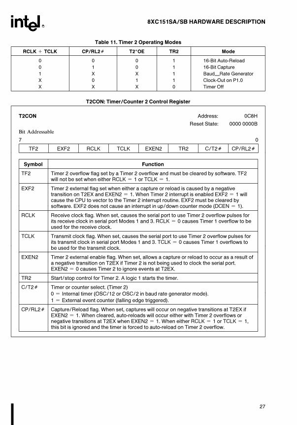
Table 11. Timer 2 Operating Modes ÀÀÀÀÀÀÀÀÀÀÀÀÀÀÀÀÀÀÀÀÀÀÀÀÀÀÀÀÀÀÀÀÀÀÀÀÀÀÀÀÀÀÀÀÀÀÀÀÀÀÀÀÀÀÀ 27
Table 12. Timer 1 Generated Commonly Used Baud Rates ÀÀÀÀÀÀÀÀÀÀÀÀÀÀÀÀÀÀÀÀÀÀÀÀÀÀÀÀÀÀÀÀÀ 44
Table 13. Timer 2 Generated Commonly Used Baud Rates ÀÀÀÀÀÀÀÀÀÀÀÀÀÀÀÀÀÀÀÀÀÀÀÀÀÀÀÀÀÀÀÀÀ 46
Table 14. Interrupt Control Matrix ÀÀÀÀÀÀÀÀÀÀÀÀÀÀÀÀÀÀÀÀÀÀÀÀÀÀÀÀÀÀÀÀÀÀÀÀÀÀÀÀÀÀÀÀÀÀÀÀÀÀÀÀÀÀÀÀÀÀ 49
Table 15. Level of Priority ÀÀÀÀÀÀÀÀÀÀÀÀÀÀÀÀÀÀÀÀÀÀÀÀÀÀÀÀÀÀÀÀÀÀÀÀÀÀÀÀÀÀÀÀÀÀÀÀÀÀÀÀÀÀÀÀÀÀÀÀÀÀÀÀÀ 52
Table 16. Interrupt Priority Within Level ÀÀÀÀÀÀÀÀÀÀÀÀÀÀÀÀÀÀÀÀÀÀÀÀÀÀÀÀÀÀÀÀÀÀÀÀÀÀÀÀÀÀÀÀÀÀÀÀÀÀÀÀ 52
Table 17. Interrupt Latency Variables ÀÀÀÀÀÀÀÀÀÀÀÀÀÀÀÀÀÀÀÀÀÀÀÀÀÀÀÀÀÀÀÀÀÀÀÀÀÀÀÀÀÀÀÀÀÀÀÀÀÀÀÀÀÀ 57
Table 18. Programming and Verifying Modes ÀÀÀÀÀÀÀÀÀÀÀÀÀÀÀÀÀÀÀÀÀÀÀÀÀÀÀÀÀÀÀÀÀÀÀÀÀÀÀÀÀÀÀÀÀÀÀ 63
Table 19. Lock Bit Function ÀÀÀÀÀÀÀÀÀÀÀÀÀÀÀÀÀÀÀÀÀÀÀÀÀÀÀÀÀÀÀÀÀÀÀÀÀÀÀÀÀÀÀÀÀÀÀÀÀÀÀÀÀÀÀÀÀÀÀÀÀÀÀ 64
Table 20. Contents of the Signature Bytes ÀÀÀÀÀÀÀÀÀÀÀÀÀÀÀÀÀÀÀÀÀÀÀÀÀÀÀÀÀÀÀÀÀÀÀÀÀÀÀÀÀÀÀÀÀÀÀÀÀ 65
Table 21. Summary of Add and Subtract Instructions ÀÀÀÀÀÀÀÀÀÀÀÀÀÀÀÀÀÀÀÀÀÀÀÀÀÀÀÀÀÀÀÀÀÀÀÀÀÀÀ 68
Table 22. Summary of Increment and Decrement Instructions ÀÀÀÀÀÀÀÀÀÀÀÀÀÀÀÀÀÀÀÀÀÀÀÀÀÀÀÀÀÀ 69
Table 23. Summary of Multiply, Divide, and Decimal-adjust Instructions ÀÀÀÀÀÀÀÀÀÀÀÀÀÀÀÀÀÀÀÀÀ 69
Table 24. Summary of Logical Instructions ÀÀÀÀÀÀÀÀÀÀÀÀÀÀÀÀÀÀÀÀÀÀÀÀÀÀÀÀÀÀÀÀÀÀÀÀÀÀÀÀÀÀÀÀÀÀÀÀÀ 70
Table 25. Summary of Move Instructions ÀÀÀÀÀÀÀÀÀÀÀÀÀÀÀÀÀÀÀÀÀÀÀÀÀÀÀÀÀÀÀÀÀÀÀÀÀÀÀÀÀÀÀÀÀÀÀÀÀÀÀ 71
Table 26. Summary of Exchange, Push, and Pop Instructions ÀÀÀÀÀÀÀÀÀÀÀÀÀÀÀÀÀÀÀÀÀÀÀÀÀÀÀÀÀÀ 72
Table 27. Summary of Bit Instructions ÀÀÀÀÀÀÀÀÀÀÀÀÀÀÀÀÀÀÀÀÀÀÀÀÀÀÀÀÀÀÀÀÀÀÀÀÀÀÀÀÀÀÀÀÀÀÀÀÀÀÀÀÀ 72
Table 28. Summary of Control Instructions ÀÀÀÀÀÀÀÀÀÀÀÀÀÀÀÀÀÀÀÀÀÀÀÀÀÀÀÀÀÀÀÀÀÀÀÀÀÀÀÀÀÀÀÀÀÀÀÀÀ 73
vii

8XC151SA/SB HARDWARE DESCRIPTION
1.0 INTRODUCTION
The 8XC151SA/SB is a highly integrated CMOS 8-bitmicrocontroller which is instruction set compatiblewith the MCSÉ51 microcontroller. It comes in 40-leadPDIP and 44-lead PLCC maintaining pin compatibilitywith MCS 51 microcontrollers. The 8XC151SA/SB has256 bytes of on-chip RAM and is available with 8/16Kbytes of on-chip ROM/OTPROM or ROMless. Sev-eral new features like programmable wait states, pagemode and Extended ALE can be selected by using thenew user programmable configuration. Key featureslike instruction pipeline, minimum of 2 clocks per in-struction and code fetch in page mode are available.
Functional characteristics of 8XC151SA/SB are listedbelow.
# Pipeline Instruction Execution Unit
# MCS 51 Microcontroller 44-pin PLCC and 40-pinPDIP Compatibility
# MCS 51 Microcontroller Compatible Instruction Set
# Static Standby to at least 16 MHz Operation
# 64K External Code Memory Space
# 64K External Data Memory Space
# 256 Bytes On-chip Data RAM
# 8/16K On-chip Code Memory (OTPROM/ROM)or ROMless Options
# 3 16-Bit Flexible Timer/Counters
# 32 Programmable I/O Lines
# 7 Maskable Interrupt Sources with 4 ProgrammablePriority Levels
# Programmable Counter Array with:
Ð High Speed Output
Ð Compare/Capture
Ð Pulse Width Modulator
Ð Watchdog Timer Capabilities
# Programmable Serial I/O Port
Ð Framing Error Detection
Ð Automatic Address Recognition
# Hardware Watchdog Timer
# External WAIT Pin
# 16-Bit Internal Code Bus
# Page Mode and Wait States Configuration Options
# Minimum 2-Clock External Code Fetch in PageMode
# User-Selectable Configurations:
Ð External Wait States (0–3 Wait States)
Ð Page Mode
# Power-Saving Features
Ð Idle Mode
Ð Power Down Mode
1

8XC151SA/SB HARDWARE DESCRIPTION
Table 1 summarizes the product names and memorydifferences of the various 8XC151SA/SB products cur-rently available. Throughout this document, the prod-ucts will generally be referred to as the C151SX.
Table 1. 8XC151 Family of Microcontrollers
ROM OTPROM ROMless OTPROM RAM
Version Version Version ROM Size Bytes
83C151SA 87C151SA 80C151SB 8K 256
83C151SB 87C151SB 80C151SB 16K 256
2.0 MEMORY ORGANIZATION
The 8XC151SA/SB devices have a separate addressspace for Program and Data Memory. Up to 64 Kbyteseach of external Program and Data Memory can beaddressed.
2.1 Program Memory
If the EAÝ pin is connected to VSS, all program fetchesare directed to external memory. On the 83C151SA (or87C151SA), if the EAÝ pin is connected to VCC, thenprogram fetches to addresses 0000H through 1FFFHare directed to internal ROM and fetches to addresses2000H through FFFFH are to external memory.
On the 83C151SB (or 87C151SB) if EAÝ is connectedto VCC, program fetches to addresses 0000H through3FFFH are directed to internal ROM, and fetches toaddresses 4000H through FFFFH are to external mem-ory.
2.2 Data Memory
The C151SX has internal data memory that is mappedinto three separate segments: the lower 128 bytes ofRAM, upper 128 bytes of RAM and 128 bytes specialfunction register (SFR). Refer to Figure 2.
The three segments are:
1. The Lower 128 bytes of RAM (addresses 00H to7FH) are directly and indirectly addressable.
2. The Upper 128 bytes of RAM (addresses 80H toFFH) are indirectly addressable only.
3. The Special Function Registers, SFRs, (addresses80H to FFH) are directly addressable only.
The Lower 128 bytes can be accessed by either direct orindirect addressing. The Upper 128 bytes can be ac-cessed by indirect addressing only. The Upper 128bytes occupy the same address space as the SFR. Thatmeans they have the same address, but are physicallyseparate from SFR space.
When an instruction accesses an internal location aboveaddress 7FH, the CPU knows whether the access is tothe upper 128 bytes of data RAM or to SFR space bythe addressing mode used in the instruction. Instruc-tions that use direct addressing access SFR space. Forexample:
MOV 0A0H,Ýdata
accesses the SFR at location 0A0H (which is P2). In-structions that use indirect addressing access the Upper128 bytes of data RAM. For example:
MOV @R0,Ýdata
where R0 contains 0A0H, accesses the data byte at ad-dress 0A0H, rather than P2 (whose address is 0A0H).
2

8XC151SA/SB HARDWARE DESCRIPTION
272832–1
Figure 1. 8XC151SA/SB Functional Block Diagram
272832–2
Figure 2. Internal Data Memory
3

8XC151SA/SB HARDWARE DESCRIPTION
3.0 SPECIAL FUNCTION REGISTERS
The special function registers (SFRs) reside in their as-sociated on-chip peripherals or in the core. Table 2shows the SFR address space with the SFR mnemonicsand reset values. Unoccupied locations in the SFR
space (the shaded locations in Table 2) are unimple-mented, i.e., no register exists. If an instruction at-tempts to write to an unimplemented SFR location, theinstruction executes, but nothing is actually written. Ifan unimplemented SFR location is read, it returns anunspecified value.
Table 2. 8XC151SA/SB Map and Reset Values
0/8 1/9 2/A 3/B 4/C 5/D 6/E 7/F
F8CH CCAP0H CCAP1H CCAP2H CCAP3H CCAP4H
FF00000000 xxxxxxxx xxxxxxxx xxxxxxxx xxxxxxxx xxxxxxxx
F0B
F700000000
E8CL CCAP0L CCAP1L CCAP2L CCAP3L CCAP4L
EF00000000 xxxxxxxx xxxxxxxx xxxxxxxx xxxxxxxx xxxxxxxx
E0ACC
E700000000
D8CCON CMOD CCAPM0 CCAPM1 CCAPM2 CCAPM3 CCAPM4
DF00x00000 00xxx000 x0000000 x0000000 x0000000 x0000000 x0000000
D0PSW PSW 1
D700000000 00000000
C8T2CON T2MOD RCAP2L RCAP2H TL2 TH2
CF00000000 xxxxxx00 00000000 00000000 00000000 00000000
C0 C7
B8IPL0 SADEN
BFx0000000 00000000
B0P3 IPH0
B711111111 x0000000
A8IE0 SADDR
AF00000000 00000000
A0P2 WDTRST
A711111111 xxxxxxxx
98SCON SBUF
9F00000000 xxxxxxxx
90P1
9711111111
88TCON TMOD TL0 TL1 TH0 TH1
8F00000000 00000000 00000000 00000000 00000000 00000000
80P0 SP DPL DPH PCON
8711111111 00000111 00000000 00000000 00xx0000
0/8 1/9 2/A 3/B 4/C 5/D 6/E 7/F
4

8XC151SA/SB HARDWARE DESCRIPTION
The following tables list the mnemonics, names, and addresses of the SFRs:
Table 3ÐCore SFRs
Table 4ÐI/O Port SFRs
Table 5ÐSerial I/O SFRs
Table 6ÐTimer/Counter and Watchdog Timer SFRs
Table 7ÐProgrammable Counter Array (PCA) SFRs
Table 3. Core SFRs
Mnemonic Name Address
ACC Accumulator E0H
B B Register F0H
PSW Program Status Word D0H
PSW1 Program Status Word 1 D1H
SP Stack Pointer 81H
DPTR Data Pointer (2 bytes) Ð
DPL Low Byte of DPTR 82H
DPH High Byte of DPTR 83H
PCON Power Control 87H
IE0 Interrupt Enable Control 0 A8H
IPH0 Interrupt Priority Control High 0 B7H
IPL0 Interrupt Priority Control Low 0 B8H
Table 4. I/O Port SFRs
Mnemonic Name Address
P0 Port 0 80H
P1 Port 1 90H
P2 Port 2 A0H
P3 Port 3 B0H
Table 5. Serial I/O SFRs
Mnemonic Name Address
SCON Serial Control 98H
SBUF Serial Data Buffer 99H
SADEN Serial Address Mask B9H
SADDR Serial Address A9H
5

8XC151SA/SB HARDWARE DESCRIPTION
Table 6. Timer/Counter and Watchdog Timer SFRs
Mnemonic Name Address
TL0 Timer/Counter 0 Low Byte 8AH
TH0 Timer/Counter 0 High Byte 8CH
TL1 Timer/Counter 1 Low Byte 8BH
TH1 Timer/Counter 1 High Byte 8DH
TL2 Timer/Counter 2 Low Byte CCH
TH2 Timer/Counter 2 High Byte CDH
TCON Timer/Counter 0 and 1 Control 88H
TMOD Timer/Counter 0 and 1 Mode Control 89H
T2CON Timer/Counter 2 Control C8H
T2MOD Timer/Counter 2 Mode Control C9H
RCAP2L Timer 2 Reload/Capture Low Byte CAH
RCAP2H Timer 2 Reload/Capture High Byte CBH
WDTRST Watchdog Timer Reset A6H
Table 7. Programmable Counter Array (PCA) SFRs
Mnemonic Name Address
CCON PCA Timer/Counter Control D8H
CMOD PCA Timer/Counter Mode D9H
CCAPM0 PCA Timer/Counter Mode 0 DAH
CCAPM1 PCA Timer/Counter Mode 1 DBH
CCAPM2 PCA Timer/Counter Mode 2 DCH
CCAPM3 PCA Timer/Counter Mode 3 DDH
CCAPM4 PCA Timer/Counter Mode 4 DEH
CL PCA Timer/Counter Low Byte E9H
CH PCA Timer/Counter High Byte F9H
CCAP0L PCA Compare/Capture Module 0 Low Byte EAH
CCAP1L PCA Compare/Capture Module 1 Low Byte EBH
CCAP2L PCA Compare/Capture Module 2 Low Byte ECH
CCAP3L PCA Compare/Capture Module 3 Low Byte EDH
CCAP4L PCA Compare/Capture Module 4 Low Byte EEH
CCAP0H PCA Compare/Capture Module 0 High Byte FAH
CCAP1H PCA Compare/Capture Module 1 High Byte FBH
CCAP2H PCA Compare/Capture Module 2 High Byte FCH
CCAP3H PCA Compare/Capture Module 3 High Byte FDH
CCAP4H PCA Compare/Capture Module 4 High Byte FEH
6
8XC151SA/SB HARDWARE DESCRIPTION
Accumulator: ACC is the Accumulator register. Themnemonics for Accumulator-Specific instructions,however, refer to the Accumulator simply as A.
B Register: The B register is used during multiply anddivide operations. For other instructions it can be treat-ed as another scratch pad register.
Stack Pointer (SP): The Stack Pointer Register is 8 bitswide. It is incremented before data is stored duringPUSH and CALL executions. The stack may resideanywhere in on-chip RAM. On reset, the Stack Pointeris initialized to 07H causing the stack to begin at loca-tion 08H.
Data Pointer: The Data Pointer (DPTR) consists of ahigh byte (DPH) and a low byte (DPL). Its intendedfunction is to hold a 16-bit address, but it may be ma-nipulated as a 16-bit register or as two independent8-bit registers.
Program Status Word: The PSW and PSW1 registerscontain program status information as detailed in PSW:Program Status Word Register on the following page.
Ports 0 to 3 Registers: P0, P1, P2, and P3 are the SFRlatches of Port 0, Port 1, Port 2, and Port 3, respective-ly.
Timer Registers: Register pairs (TH0, TL0), (TH1,TL1), and (TH2, TL2) are the 16-bit count registers forTimer/Counters 0, 1, and 2 respectively. Control andstatus bits are contained in registers TCON and TMODfor Timers 0 and 1 and in registers T2CON andT2MOD for Timer 2. The register pair (RCAP2H,RCAP2L) are the capture/reload registers for Timer 2in 16-bit capture mode or 16-bit auto-reload mode.
Programmable Counter Array (PCA) Registers: The16-bit PCA timer/counter consists of registers CH andCL. Registers CCON and CMOD contain the controland status bits for the PCA. The CCAPMn (n e 0, 1,2, 3, or 4) registers control the mode for each of the fivePCA modules. The register pairs (CCAPnH, CCAPnL)are the 16-bit compare/capture registers for each PCAmodule.
Serial Port Registers: The Serial Data Buffer, SBUF,is actually two separate registers: a transmit buffer anda receive buffer register. When data is moved to SBUF,it goes to the transmit buffer where it is held for serialtransmission. (Moving a byte to SBUF initiates thetransmission). When data is moved from SBUF, itcomes from the receive buffer. Register SCON containsthe control and status bits for the Serial Port. RegistersSADDR and SADEN are used to define the Given andthe Broadcast addresses for the Automatic AddressRecognition feature.
Interrupt Registers: The individual interrupt enablebits are in the IE0 register. Priorities of interrupt can beset in the IPH0 and IPL0 registers.
Power Control Register: PCON controls the PowerReduction Modes. Idle and Power Down Modes.
Watchdog Timer Reset: WDTRST register is used tokeep the watchdog timer from periodically resetting thepart.
7

8XC151SA/SB HARDWARE DESCRIPTION
PSW: Program Status Word Register
PSW Address: D0H
Reset State: 0000 0000B
Program Status Word. PSW contains bits that reflect the results of operations, bits that select the registerbank for registers R0–R7, and two general-purpose flags that are available to the user.
7 0
CY AC F0 RS1 RS0 OV UD P
BitFunction
Mnemonic
CY Carry Flag:
The carry flag is set by an addition instruction (ADD, ADDC) if there is a carry out of theMSB. It is set by a subtraction (SUB, SUBB) if a borrow is needed for the MSB. Thecarry flag is also affected by some rotate and shift instructions, logical bit instructions,bit move instructions, and the multiply (MUL) and decimal adjust (DA) instructions.
AC Auxillary Carry Flag:
The auxillary carry flag is affected only by instructions that address 8-bit operands. TheAC flag is set if an arithmetic instruction with an 8-bit operand produces a carry out of bit13 (from addition) or a borrow into bit 3 (from subtraction). Otherwise it is cleared. Thisflag is useful for BCD arithmetic.
F0 Flag 0:
This general-purpose flag is available to the user.
RS1:0 Register Bank Select Bits 1 and 0:
These bits select the memory locations that comprise the active bank of the register file(registers R0–R7).
RS1 RS0 Bank Address
0 0 0 00H–07H
0 1 1 08H–0FH
1 0 2 10H–17H
1 1 3 18H–1FH
OV Overflow Flag:
This bit is set if an addition or subtraction of signed variables results in an overflow error(i.e., if the magnitude of the sum or difference is too great for the seven LSBs in 2’s-complement representation). The overflow flag is also set if a multiplication productoverflows one byte or if a division by zero is attempted.
UD User-defined Flag:
This general-purpose flag is available to the user.
P Parity Bit:
This bit indicates the parity if the accumulator. It is set if an odd number of bits in theaccumulator are set. Otherwise, it is cleared. Not all instructions update the parity bit.The parity bit is set or cleared by instructions that change the contents of theaccumulator (ACC, Register R11).
8

8XC151SA/SB HARDWARE DESCRIPTION
PSW1 Address: 0D1H
Reset State: 0000 0000B
7 0
CY AC F0 RS1 RS0 OV Z Ð
BitFunction
Mnemonic
CY Carry Flag:
Identical to the CY bit in the PSW register.
AC Auxillary Carry Flag:
Identical to the AC bit in the PSW register.
N Negative Flag:
This bit is set if the result of the last logical or arithmetic operation was negative, i.e., bit15 e 1. Otherwise it is cleared.
RS1:0 Register Bank Select Bits 0 and 1:
Identical to the RS1:0 bits in the PSW register.
OV Overflow Flag:
Identical to the OV bit in the PSW register.
Z Zero Flag:
This flag is set if the result of the last logical or arithmetic operation is zero. Otherwise itis cleared.
Ð Reserved:
The value read from this bit is indeterminate. Do not write a ‘‘1’’ to this bit.
9

8XC151SA/SB HARDWARE DESCRIPTION
4.0 PORT STRUCTURES ANDOPERATION
The C151SX uses input/output (I/O) ports to ex-change data with external devices. In addition to per-forming general-purpose I/O, some ports are capable ofexternal memory operations; others allow for alternatefunctions. All four C151SX I/O ports are bidirectional.Each port contains a latch, an output driver, and aninput buffer. Port 0 and port 2 output drivers and inputbuffers facilitate external memory operations. Port 0drives the lower address byte onto the parallel addressbus, and port 2 drives the upper address byte onto thebus. In nonpage mode, the data is multiplexed with thelower address byte on port 0. In page mode, the data ismultiplexed with the upper address byte on port 2. Allport 1 and port 3 pins serve for both general-purposeI/O and alternative functions.
4.1 I/O Configurations
Each port SFR operates via type-D latches, as illustrat-ed in Figure 3 for ports 1 and 3. A CPU ‘‘write tolatch’’ signal initiates transfer of internal bus data intothe type-D latch. A CPU ‘‘read latch’’ signal transfersthe latched Q output onto the internal bus. Similarly, a‘‘read pin’’ signal transfers the logical level of the portpin. Some port data instructions activate the ‘‘readlatch’’ signal while others activate the ‘‘read pin’’ sig-nal. Latch instructions are referred to as read-modify-write instructions. Each I/O line may be independentlyprogrammed as input or output.
4.2 Port 1 and Port 3
Figure 3 shows the structure of ports 1 and 3, whichhave internal pullups. An external source can pull thepin low. Each port pin can be configured either forgeneral-purpose I/O or for its alternate input or outputfunction.
To use a pin for general-purpose output, set or clear thecorresponding bit in the Px register (x e 1, 3). To use apin for general-purpose input, set the bit in the Px reg-ister. This turns off the output driver FET.
To configure a pin for its alternate function, set the bitin the Px register. When the latch is set, the ‘‘alternateoutput function’’ signal controls the output level (Fig-ure 3). The operation of ports 1 and 3 is discussed fur-ther in the ‘‘Quasi-bidirectional Port Operation’’ sec-tion.
4.3 Port 0 and Port 2
Ports 0 and 2 are used for general-purpose I/O or asthe external address/data bus. Port 0, shown in Figure4, differs from the other ports in not having internalpullups. Figure 5 shows the structure of port 2. Anexternal source can pull a port 2 pin low.
To use a pin for general-purpose output, set or clear thecorresponding bit in the Px register (x e 0, 2). To use apin for general-purpose input set the bit in the Px regis-ter to turn off the output driver FET.
10
8XC151SA/SB HARDWARE DESCRIPTION
272832–3
Figure 3. Port 1 and Port 3 Structure
272832–4
Figure 4. Port 0 Structure
11

8XC151SA/SB HARDWARE DESCRIPTION
272832–5
Figure 5. Port 2 Structure
When port 0 and port 2 are used for an external memo-ry cycle, an internal control signal switches the output-driver input from the latch output to the internal ad-dress/data line. Port 0 and port 2 are precluded fromuse as general purpose I/O ports when used as address/data bus drivers.
Port 0 internal pullups assist the logic-one output formemory bus cycles only. Except for these bus cycles,the pullup FET is off. All other port 0 outputs are opendrain.
12

8XC151SA/SB HARDWARE DESCRIPTION
4.4 Read-Modify-Write Instructions
Some instructions read the latch data rather than thepin data. The latch based instructions read the data,modify the data, and then rewrite the latch. These arecalled ‘‘read-modify-write’’ instructions. Below is acomplete list of these special instructions. When thedestination operand is a port, or a port bit, these in-structions read the latch rather than the pin:
ANL (logical AND, e.g., ANLP1, A)
ORL (logical OR, e.g., ORLP2, A)
XRL (logical EX-OR, e.g.,XRL P3, A)
JBC (jump if bit 4 1 andclear bit, e.g.,JBC P1.1, LABEL)
CPL (complement bit, e.g.,CPL P3.0)
INC (increment, e.g., INCP2)
DEC (decrement, e.g., DECP2)
DJNZ (decrement and jump ifnot zero, e.g.,DJNZ P3, LABEL)
MOV PX.Y, C (move carry bit to bitY of port X)
CLR PX.Y (clear bit Y of port X)
SETB PX.Y (set bit Y of port X)
It is not obvious the last three instructions in this listare read-modify-write instructions. These instructionsread the port (all 8 bits), modify the specifically ad-dressed bit, and write the new byte back to the latch.These read-modify-write instructions are directed tothe latch rather than the pin in order to avoid possiblemisinterpretation of voltage (and therefore, logic) levelsat the pin. For example, a port bit used to drive thebase of an external bipolar transistor cannot rise abovethe transistor’s base-emitter junction voltage (a valuelower than VIL). With a logic one written to the bit,attempts by the CPU to read the port at the pin aremisinterpreted as logic zero. A read of the latch ratherthan the pin returns the correct logic-one value.
4.5 Quasi-Bidirectional Port Operation
Port 1, port 2, and port 3 have fixed internal pullupsand are referred to as ‘‘quasi-bidirectional’’ ports.When configured as an input, the pin impedance ap-pears as logic one and sources current in response to anexternal logic-zero condition. Port 0 is a ‘‘true bidirec-tional’’ pin. The pin floats when configured as input.Resets write logical one to all port latches. If logicalzero is subsequently written to a port latch, it can bereturned to input conditions by a logical one written tothe latch. For additional electrical information, refer tothe current 8XC151SA/SB datasheet.
13

8XC151SA/SB HARDWARE DESCRIPTION
272832–6
Figure 6. Internal Pullup Configurations
Logical zero-to-one transitions in port 1, port 2, andport 3 utilize an additional pullup to aid this logic tran-sition (see Figure 6). This increases switch speed. Theextra pullup briefly sources 100 times normal internalcircuit current. The internal pullups are field-effecttransistors rather than linear resistors. Pullups consistof three p-channel FET (pFET) devices. A pFET is onwhen the gate senses logical zero and off when the gatesenses logical one. pFET Ý1 is turned on for two oscil-lator periods immediately after a zero-to-one transitionin the port latch. A logic one at the port pin turns onpFET Ý3 (a weak pullup) through the inverter. Thisinverter and pFET pair form a latch to drive logic one.pFET Ý2 is a very weak pullup switched on wheneverthe associated nFET is switched off. This is traditionalCMOS switch convention. Current strengths are (/10
that of pFET Ý3.
4.6 Port Loading
Output buffers of port 1, port 2, and port 3 can eachsink 1.6 mA at logic zero (see VOL specifications in the8XC151SA/SB datasheet). These port pins can be driv-en by open-collector and open-drain devices. Logiczero-to-one transitions occur slowly as limited currentpulls the pin to a logic-one condition (Figure 6). A log-ic-zero input turns off pFET Ý3. This leaves onlypFET Ý2 weakly in support of the transition. In exter-nal bus mode, port 0 output buffers each sink 3.2 mA atlogic zero (see VOL1 in the 8XC151SA/SB datasheet).However, the port 0 pins require external pullups todrive external gate inputs. See the latest revision of the8XC151SA/SB datasheet for complete electrical designinformation. External circuits must be designed to limitcurrent requirements to these conditions.
14

8XC151SA/SB HARDWARE DESCRIPTION
4.7 Accessing External Memory
The external memory interface comprises the externalbus (ports 0 and 2) and the bus control signals. Chipconfiguration bytes determine several interface options:page mode or nonpage mode for external code fetches;the address ranges for RDÝ, WRÝ, and PSENÝ; andthe number of external wait states. You can use theseoptions to tailor the interface to your application.
The external memory interface operates in either pagemode and nonpage mode. Page mode provides in-creased performance by reducing the time for externalcode fetches. Page mode does not apply to code fetchesfrom on-chip memory. The reset routine configures theC151SX for operation in page mode or nonpage modeaccording to bit 1 of configuration bytes UCONFIG0(refer to Table 8). Figure 7 shows the structure of theexternal address bus for page and nonpage mode opera-tion. P0 carries address A7:0 while P2 carries addressA15:8. Data D7:0 is multiplexed with A7:0 on P0 innonpage mode and with A15:8 on P2 in page mode.
272832–7
Figure 7. Bus Structure in Nonpage Mode and Page Mode
²The descriptions of A15:8/P2.7:0 and AD7:0/P0.7:0 are for the nonpage-mode chip configuration (compatible with 44-pin PLCC MCSÉ 51microcontrollers). If the chip is configured for page-mode operation, port 0 carries the lower address bits (A7:0), and port 2 carries the upperaddress bits (A15:8) and the data (D7:0).
15

8XC151SA/SB HARDWARE DESCRIPTION
Table 8. User Configuration Byte UCONFIG0
UConfig0 Address: FFF8H
Ð WSa1Ý WSa0Ý XALEÝ Ð Ð PageÝ Ð
MSB LSB
BitFunction
Mnemonic
WSa1Ý Wait State Select for External Code
WSa1Ý WSa0Ý Description
1 1 No Wait State
1 0 Insert 1 Code Wait State
0 1 Insert 2 Code Wait State
0 0 Insert 3 Code Wait State
XALEÝ Extended ALE
XALEÝ Description
1 ALE pulse e 1 Clock Period
0 ALE pulse e 3 Clock Period (Additional 1 Wait State)
PageÝ Page Mode Select
PageÝ Description
1 Non-Page Mode (A15:8 on Port 2, A7:0/D7:0 on Port 0)
0 Page-Mode (A15:8/D7:0 on Port 2, A7:0 on Port 0)
Table 9. User Configuration Byte UCONFIG1
UConfig1 Address: FFF9H
Ð Ð Ð Ð Ð WSb1Ý WSb0Ý Ð
MSB LSB
BitFunction
Mnemonic
WSb1Ý Wait State Select for External Data
WSb1Ý WSb0Ý Description
1 1 No Wait State
1 0 Insert 1 Data Wait State
0 1 Insert 2 Data Wait State
0 0 Insert 3 Data Wait State
16

8XC151SA/SB HARDWARE DESCRIPTION
Table 10. Bus Cycle Definitions (No Wait States)
Mode Bus CycleBus Activity
State 1 State 2 State 3
Nonpage Code Read ALE RDÝ/PSENÝ, Code In
ModeData Read (Note 2) ALE RDÝ/PSENÝ Data In
Data Write (Note 2) ALE WRÝ WRÝ High, Data Out
Page Code Read, Page Miss ALE RDÝ/PSENÝ, Code In
ModeCode Read, Page Hit (Note 3) PSENÝ, Code In
Data Read (Note 2) ALE RDÝ/PSENÝ Data In
Data Write (Note 2) ALE WRÝ WRÝ High, Data Out
NOTES:1. Signal timing implied by this table is approximate (idealized).2. Data read (page mode) e data read (nonpage mode) and write (page mode) e write (nonpage mode) except that inpage mode data appears on P2 (multiplexed with A15:0), whereas in nonpage mode data appears on P0 (multiplexed withA7:0).3. The initial code read page hit bus cycle can execute only following a code read page miss cycle.
4.7.1 BUS CYCLE DEFINITION
Table 10 lists the types of external bus cycles. It alsoshows the activity on the bus for nonpage mode andpage mode bus cycles with no wait states. There arethree types of nonpage mode bus cycles: code read, dataread, and data write. There are four types of page modebus cycles: code read (page miss), code read (page hit),data read, and data write. The data read and data writecycles are the same for page mode and nonpage mode(except the multiplexing of D7:0 on ports 0 and 2).
In nonpage mode, the external bus structure is the sameas for MCS 51 microcontrollers. The upper address bits(A15:8) are on port 2, and the lower address bits (A7:0)are multiplexed with the data (D7:0) on port 0. Exter-nal code read bus cycles execute in approximately twostate times. See Table 10 and Figure 8. External dataread bus cycles (Figure 9) and external write bus cycles(Figure 10) execute in approximately three state times.For the write cycle (Figure 10), a third state is append-ed to provide recovery time for the bus.
272832–8
Figure 8. External Bus Cycle: Code Fetch, Nonpage Mode
17

8XC151SA/SB HARDWARE DESCRIPTION
272832–9
Figure 9. External Bus Cycle: Data Read, Nonpage Mode
272832–10
Figure 10. External Bus Cycle: Data Write, Nonpage Mode
18

8XC151SA/SB HARDWARE DESCRIPTION
Page mode increases performance by reducing the timefor external code fetches. Under certain conditions thecontroller fetches an instruction from external memoryin one state time instead of two. Page mode does notaffect internal code fetches.
The first code fetch to a 256-byte ‘‘page’’ of memoryalways uses a two-state bus cycle. Subsequent succes-sive code fetches to the same page (page hits ) requireonly a one-state bus cycle. When a subsequent fetch isto a different page (a page miss ) it again requires a two-state bus cycle. The following external code fetches arealways page-miss cycles:
# the first external code fetch after a page rollover²
# the first external code fetch after an external databus cycle
# the first external code fetch after powerdown or idlemode
# the first external code fetch after a branch, return,interrupt, etc.
Figure 11 shows the two types of external bus cycles forcode fetches in page mode. The page-miss cycle is thesame as a code fetch cycle in nonpage mode (exceptD7:0 is multiplexed with A15:8 on P2). For the page-hitcycle, the upper eight address bits are the same as forthe preceding cycle. Therefore, ALE is not asserted,and the values of A15:8 are retained in the addresslatches. In a single state, the new values of A7:0 areplaced on port 0, and memory places the instructionbyte on port 2. Notice that a page hit reduces the avail-able address access time by one state. Therefore, fastermemories may be required to support page mode.
The bus cycles for data reads and data writes in pagemode are identical to those for nonpage mode, exceptfor the different signals on ports 0 and 2.
²A page rollover occurs when the address increments from the top of one 256-byte page to the bottom of the next (e.g., from FAFFH to FB00H).
19
8XC151SA/SB HARDWARE DESCRIPTION
272832–11
²During a sequence of page hits, PSENÝ remains low until the end of the last page-hit cycle.
Figure 11. External Bus Cycle: Code Fetch, Page Mode
272832–12
Figure 12. External Bus Cycle: Data Read, Page Mode
20
8XC151SA/SB HARDWARE DESCRIPTION
272832–13
Figure 13. External Bus Cycle: Data Write, Page Mode
4.7.2 EXTERNAL BUS CYCLES WITH WAITSTATES
The C151SX can be configured to add wait states to theexternal bus cycles by extending the RDÝ/WRÝ/PSENÝ pulses or by extending the ALE pulse. Config-uration bites WAS1:0Ý and WSB1:0Ý specify 0, 1, 2,
or 3 wait states for RDÝ/WRÝ/PSENÝ. TheXALEÝ configuration bit specifies 0 or 1 wait state forALE. You can also configure the chip to use both typesof wait states. Accesses to on-chip code and data mem-ory always use zero wait states.
272832–14
Figure 14. External Bus Cycle: Data Write with One WRÝ Wait State (Nonpage Mode)
21

8XC151SA/SB HARDWARE DESCRIPTION
272832–15
Figure 15. External Bus Cycle: Code Fetch with One ALE Wait State (Nonpage Mode)
Figure 15 shows the nonpage mode code fetch externalbus cycle with ALE extended. The wait state extendsthe bus cycle from two states to three. For read andwrite external bus cycles, the extended ALE extendsthe bus cycle from three states to four.
4.7.3 PORT 0 AND PORT 2 FOR STATES INNON-PAGE AND PAGE MODE
In nonpage mode the port pins have the same signals asthose on the 8XC51FX. For an external memory in-struction using a 16-bit address, the port pins carry ad-dress and data bits during the bus cycle. However, ifthe instruction uses an 8-bit address (e.g., MOVX@Ri),the contents of P2 are driven onto the pins. These pinsignals can be used to select 256-bit pages in externalmemory.
During a bus cycle, the CPU always writes FFH to P0,and the former contents of P0 are lost. A bus cycle doesnot change the contents of P2. When the bus is idle, theport 0 pins are held at high impedance, and the con-tents of P2 are driven onto the port 2 pins.
In a page-mode bus cycle, the data is multiplexed withthe upper address byte on port 2. However, if the in-struction uses an 8-bit address (e.g., MOVX@Ri), thecontents of P2 are driven onto the pins when data is noton the pins. These logic levels can be used to select 256-bit pages in external memory. During bus idle, the port0 and port 2 pins are held at high impedance.
22

8XC151SA/SB HARDWARE DESCRIPTION
5.0 TIMERS/COUNTERS
The C151SX has three 16-bit Timer/Counters: Timer0, Timer 1, and Timer 2. Each consists of two 8-bitregisters, THx and TLx, (x e 0, 1, and 2). All threecan be configured to operate either as timers or eventcounters.
In the Timer function, the TLx register is incrementedevery machine cycle. Thus one can think of it as count-ing machine cycles. Since a machine cycle consists of 12oscillator periods, the count rate is (/12 of the oscillatorfrequency.
In the Counter function, the register is incremented inresponse to a 1-to-0 transition at its corresponding ex-ternal input pinÐT0, T1, or T2. In this function, theexternal input is sampled during S5P2 of every machinecycle. When the samples show a high in one cycle and alow in the next cycle, the count is incremented. Thenew count value appears in the register during S3P1 ofthe cycle following the one in which the transition wasdetected. Since it takes 2 machine cycles (24 oscillatorperiods) to recognize a 1-to-0 transition, the maximumcount rate is (/24 of the oscillator frequency. There areno restrictions on the duty cycle of the external inputsignal, but to ensure that a given level is sampled atleast once before it changes, it should be held for atleast one full machine cycle.
In addition to the Timer or Counter selection, Timer 0and Timer 1 have four operating modes from which toselect: Modes 0 – 3. Timer 2 has three modes of opera-tion: Capture, Auto-Reload, and Baud Rate Generator.
5.1 Timer 0 and Timer 1
The Timer or Counter function is selected by controlbits C/TÝ in the Special Function Register TMOD.These two Timer/Counters have four operating modes,which are selected by bit-pairs (M1, M0) in TMOD.Modes 0, 1, and 2 are the same for both Timer/Coun-ters. Mode 3 operation is different for the two timers.
MODE 0
Either Timer 0 or Timer 1 in Mode 0 is an 8-bit Coun-ter with a divide-by-32 prescaler. Figure 16 shows theMode 0 operation for either timer.
In this mode, the Timer register is configured as a13-bit register. As the count rolls over from all 1s to all0s, it sets the Timer interrupt flag TFx. The countedinput is enabled to the Timer when TRx e 1 and eitherGATE e 0 or INTxÝ e 1. (Setting GATE e 1 al-lows the Timer to be controlled by external inputINTxÝ, to facilitate pulse width measurements). TRxand TFx are control bits in SFR TCON. The GATE bitis in TMOD. There are two different GATE bits, onefor Timer 1 (TMOD.7) and one for Timer 0(TMOD.3).
The 13-bit register consists of all 8 bits of THx and thelower 5 bits of TLx. The upper 3 bits of TLx are inde-terminate and should be ignored. Setting the run flag(TRx) does not clear these registers.
MODE 1
Mode 1 is the same as Mode 0, except that the Timerregister uses all 16 bits. Refer to Figure 17. In thismode, THx and TLx are cascaded; there is no prescal-er.
MODE 2
Mode 2 configures the Timer register as an 8-bit Coun-ter (TLx) with automatic reload, as shown in Figure 18.Overflow from TLx not only sets TFx, but also reloadsTLx with the contents of THx, which is preset by soft-ware. The reload leaves THx unchanged.
23

8XC151SA/SB HARDWARE DESCRIPTION
TMOD: Timer/Counter Mode Control Register
TMOD Address: 089H
Reset State: 0000 0000B
Not Bit Addressable
7 TIMER 1 Timer 0 0
GATE C/TÝ M1 M0 GATE C/TÝ M1 M0
Symbol Function
GATE Gating control when set. Timer/Counter 0 or 1 is enabled only while INT0Ý or INT1Ý pinis high and TR0 or TR1 control pin is set. When cleared, Timer 0 or 1 is enabled wheneverTR0 or TR1 control bit is set.
C/TÝ Timer or Counter Selector. Clear for Timer operation (input from internal system clock). Setfor Counter operation (input from T0 or T1 input pin).
M1 M0 Operating Mode
0 0 8-bit Timer/Counter. THx with Tlx as 5-bit prescaler.
0 1 16-bit Timer/Counter. THx and TLx are cascaded; there is no prescaler.
1 0 8-bit auto-reload Timer/Counter. THx holds a value which is to be reloaded intoTLx each time it overflows.
1 1 (Timer 0) TL0 is an 8-bit Timer/Counter controlled by the standard Timer 0control bits. TH0 is an 8-bit timer only controlled by Timer 1 control bits.
1 1 (Timer 1) Timer/Counter stopped.
x e 0 or 1
272832–16
Figure 16. Timer/Counter 0 or 1 in Mode 0: 13-Bit Counter
24

8XC151SA/SB HARDWARE DESCRIPTION
TCON: Timer/Counter Control Register
TCON Address: 088H
Reset State: 0000 0000B
Bit Addressable
7 0
TF1 TR1 TF0 TR0 IE1 IT1 IE0 IT0
Symbol Function
TF1 Timer 1 overflow Flag. Set by hardware on Timer/Counter overflow. Cleared by hardwarewhen processor vectors to interrupt routine.
TR1 Timer 1 Run control bit. Set/cleared by software to turn Timer/Counter 1 on/off.
TF0 Timer 0 overflow Flag. Set by hardware on Timer/Counter 0 overflow. Cleared by hardwarewhen processor vectors to interrupt routine.
TR0 Timer 0 Run control bit. Set/cleared by software to turn Timer/Counter 0 on/off.
IE1 Interrupt 1 flag. Set by hardware when external interrupt 1 edge is detected (transmitted orlevel-activated). Cleared when interrupt processed only if transition-activated.
IT1 Interrupt 1 Type control bit. Set/cleared by software to specify falling edge/low leveltriggered external interrupt 1.
IE0 Interrupt 0 flag. Set by hardware when external interrupt 0 edge is detected (transmitted orlevel-activated). Cleared when interrupt processed only if transition-activated.
IT0 Interrupt 0 Type control bit. Set/cleared by software to specify falling edge/low leveltriggered external interrupt 0.
x e 0 or 1
272832–17
Figure 17. Timer/Counter 0 or 1 in Mode 1: 16-Bit Counter
MODE 3
Timer 1 in Mode 3 simply holds its count. The effect isthe same as setting TR1 e 0.
Timer 0 in Mode 3 establishes TL0 and TH0 as twoseparate counters. The logic for Mode 3 on Timer 0 isshown in Figure 19. TL0 uses the Timer 0 control bits:C/TÝ, GATE, TR0, INT0Ý, and TF0. TH0 is locked
25

8XC151SA/SB HARDWARE DESCRIPTION
x e 0 or 1272832–18
Figure 18. Timer/Counter 1 Mode 2: 8-Bit Auto-Reload
272832–19
Figure 19. Timer/Counter 0 Mode 3: Two 8-Bit Counters
into a timer function (counting machine cycles) andtakes over the use of TR1 and TF1 from Timer 1. ThusTH0 now controls the Timer 1 interrupt.
Mode 3 is provided for applications requiring an extra8-bit timer or counter. When Timer 0 is in Mode 3,Timer 1 can be turned on and off by switching it out ofand into its own Mode 3, or can still be used by theserial port as a baud rate generator, or in any applica-tion not requiring an interrupt.
5.2 Timer 2
Timer 2 is a 16-bit Timer/Counter which can operateeither as a timer or as an event counter. This is selectedby bit C/T2Ý in the Special Function RegisterT2CON. It has three operating modes: capture, auto-reload (up or down counting), and baud rate generator.The modes are selected by bits in T2CON as shown inTable 11.
26
8XC151SA/SB HARDWARE DESCRIPTION
Table 11. Timer 2 Operating Modes
RCLK a TCLK CP/RL2Ý T2*OE TR2 Mode
0 0 0 1 16-Bit Auto-Reload
0 1 0 1 16-Bit Capture
1 X X 1 BaudÐRate Generator
X 0 1 1 Clock-Out on P1.0
X X X 0 Timer Off
T2CON: Timer/Counter 2 Control Register
T2CON Address: 0C8H
Reset State: 0000 0000B
Bit Addressable
7 0
TF2 EXF2 RCLK TCLK EXEN2 TR2 C/T2Ý CP/RL2Ý
Symbol Function
TF2 Timer 2 overflow flag set by a Timer 2 overflow and must be cleared by software. TF2will not be set when either RCLK e 1 or TCLK e 1.
EXF2 Timer 2 external flag set when either a capture or reload is caused by a negativetransition on T2EX and EXEN2 e 1. When Timer 2 interrupt is enabled EXF2 e 1 willcause the CPU to vector to the Timer 2 interrupt routine. EXF2 must be cleared bysoftware. EXF2 does not cause an interrupt in up/down counter mode (DCEN e 1).
RCLK Receive clock flag. When set, causes the serial port to use Timer 2 overflow pulses forits receive clock in serial port Modes 1 and 3. RCLK e 0 causes Timer 1 overflow to beused for the receive clock.
TCLK Transmit clock flag. When set, causes the serial port to use Timer 2 overflow pulses forits transmit clock in serial port Modes 1 and 3. TCLK e 0 causes Timer 1 overflows tobe used for the transmit clock.
EXEN2 Timer 2 external enable flag. When set, allows a capture or reload to occur as a result ofa negative transition on T2EX if Timer 2 is not being used to clock the serial port.EXEN2 e 0 causes Timer 2 to ignore events at T2EX.
TR2 Start/stop control for Timer 2. A logic 1 starts the timer.
C/T2Ý Timer or counter select. (Timer 2)
0 e Internal timer (OSC/12 or OSC/2 in baud rate generator mode).
1 e External event counter (falling edge triggered).
CP/RL2Ý Capture/Reload flag. When set, captures will occur on negative transitions at T2EX ifEXEN2 e 1. When cleared, auto-reloads will occur either with Timer 2 overflows ornegative transitions at T2EX when EXEN2 e 1. When either RCLK e 1 or TCLK e 1,this bit is ignored and the timer is forced to auto-reload on Timer 2 overflow.
27
8XC151SA/SB HARDWARE DESCRIPTION
272832–20
Figure 20. Timer 2 in Capture Mode
CAPTURE MODE
In the capture mode there are two options selected bybit EXEN2 in T2CON. If EXEN2 e 0, Timer 2 is a16-bit timer or counter which upon overflow sets bitTF2 in T2CON. This bit can then be used to generatean interrupt. If EXEN2 e 1, Timer 2 still does theabove, but with the added feature that a 1-to-0 tran-sition at external input T2EX causes the current valuein the Timer 2 registers, TH2 and TL2, to be capturedinto registers RCAP2H and RCAP2L, respectively. Inaddition, the transition at T2EX causes bit EXF2 inT2CON to be set. The EXF2 bit, like TF2, can generatean interrupt. The capture mode is illustrated in Figure20.
AUTO-RELOAD MODE(UP OR DOWN COUNTER)
Timer 2 can be programmed to count up or down whenconfigured in its 16-bit auto-reload mode. This featureis invoked by a bit named DCEN (Down Counter En-able) located in the SFR T2MOD. Upon reset theDCEN bit is set to 0 so that Timer 2 will default tocount up. When DCEN is set, Timer 2 can count up ordown depending on the value of the T2EX pin.
28
8XC151SA/SB HARDWARE DESCRIPTION
T2MOD: Timer 2 Mode Control Register
T2MOD Address: 0C9H
Reset State: XXXX XX00B
Not Bit Addressable
7 0
Ð Ð Ð Ð Ð Ð T2OE DCEN
Symbol Function
Ð Not implemented, reserved for future use.*
T2OE Timer 2 Output Enable bit.
DCEN Down Count Enable bit. When set, this allows Timer 2 to be configured as an up/downcounter.
NOTE:*User software should not write 1s to reserved bits. These bits may be used in future 8051 family products to invokenew features. In that case, the reset or inactive value of the new bit will be 0, and its active value will be 1. The valueread from a reserved bit is indeterminate.
272832–21
Figure 21. Timer 2 Auto Reload Mode (DCEN e 0)
29

8XC151SA/SB HARDWARE DESCRIPTION
Figure 21 shows Timer 2 automatically counting upwhen DCEN e 0. In this mode there are two optionsselected by bit EXEN2 in T2CON. If EXEN2 e 0,Timer 2 counts up to 0FFFFH and then sets the TF2bit upon overflow. The overflow also causes the timerregisters to be reloaded with the 16-bit value inRCAP2H and RCAP2L. The values in RCAP2H andRCAP2L are preset by software. If EXEN2 e 1, a 16-bit reload can be triggered either by an overflow or by a1-to-0 transition at external input T2EX. This tran-sition also sets the EXF2 bit. Either the TF2 or EXF2bit can generate the Timer 2 interrupt if it is enabled.
Setting the DCEN bit enables Timer 2 to count up ordown as shown in Figure 22. In this mode the T2EXpin controls the direction of count. A logic 1 at T2EXmakes Timer 2 count up. The timer will overflow at0FFFFH and set the TF2 bit which can then generatean interrupt if it is enabled. This overflow also causesthe 16-bit value in RCAP2H and RCAP2L to be re-loaded into the timer registers, TH2 and TL2, respec-tively.
A logic 0 at T2EX makes Timer 2 count down. Nowthe timer underflows when TH2 and TL2 equal thevalues stored in RCAP2H and RCAP2L. The under-flow sets the TF2 bit and causes 0FFFFH to be reload-ed into the timer registers.
The EXF2 bit toggles whenever Timer 2 overflows orunderflows. This bit can be used as a 17th bit of resolu-tion if desired. In this operating mode, EXF2 does notgenerate an interrupt.
BAUD RATE GENERATOR MODE
The baud rate generator mode is selected by setting theRCLK and/or TCLK bits in T2CON. Timer 2 in thismode will be described in conjunction with the serialport.
PROGRAMMABLE CLOCK OUT
A 50% duty cycle clock can be programmed to comeout on P1.0. This pin, besides being a regular I/O pin,has two alternate functions. It can be programmed (1)to input the external clock for Timer/Counter 2 or (2)to output a 50% duty cycle clock ranging from 61 Hzto 4 MHz at a 16 MHz operating frequency.
To configure the Timer/Counter 2 as a clock generator,bit C/T2Ý (in T2CON) must be cleared and bit T2OEin T2MOD must be set. Bit TR2 (T2CON.2) also mustbe set to start the timer.
The Clock-out frequency depends on the oscillator fre-quency and the reload value of Timer 2 capture regis-ters (RCAP2H, RCAP2L) as shown in this equation:
Clock-out Frequency e
Oscillator Frequency
4 c (65536 b RCAP2H, RCAP2L)
In the Clock-Out mode Timer 2 roll-overs will not gen-erate an interrupt. This is similar to when Timer 2 isused as a baud-rate generator. It is possible to use Tim-er 2 as a baud-rate generator and a clock generatorsimultaneously. Note, however, that the baud-rate andClock-out frequencies cannot be determined indepen-dently of one another since they both use the values inRCAP2H and RCAP2L.
6.0 PROGRAMMABLE COUNTERARRAY
The Programmable Counter Array (PCA) consists of a16-bit timer/counter and five 16-bit compare/capturemodules as shown in Figure 24. The PCA timer/coun-ter serves as a common time base for the five modulesand is the only timer which can service the PCA. Itsclock input can be programmed to count any one of thefollowing signals:
# oscillator frequency d 12
# oscillator frequency d 4
# Timer 0 overflow
# external input on ECI (P1.2).
Each compare/capture module can be programmed inany one of the following modes:
# rising and/or falling edge capture
# software timer
# high speed output
# pulse width modulator.
Module 4 can also be programmed as a watchdog tim-er.
When the compare/capture modules are programmedin the capture mode, software timer, or high speed out-put mode, an interrupt can be generated when the mod-ule executes its function. All five modules plus the PCAtimer overflow share one interrupt vector (more aboutthis in the PCA Interrupt section).
30

8XC151SA/SB HARDWARE DESCRIPTION
272832–22
Figure 22. Timer 2 Auto Reload Mode (DCEN e 1)
272832–23
Figure 23. Timer 2 in Clock-Out Mode
31
8XC151SA/SB HARDWARE DESCRIPTION
272832–24
Figure 24. Programmable Counter Array
The PCA timer/counter and compare/capture modulesshare Port 1 pins for external I/O. These pins are listedbelow. If the port pin is not used for the PCA, it canstill be used for standard I/O.
PCA Component External I/O Pin
16-bit Counter P1.2 / ECI
16-bit Module 0 P1.3 / CEX0
16-bit Module 1 P1.4 / CEX1
16-bit Module 2 P1.5 / CEX2
16-bit Module 3 P1.6 / CEX3
16-bit Module 4 P1.7 / CEX4
6.1 PCA 16-Bit Timer/Counter
The PCA has a free-running 16-bit timer/counter con-sisting of registers CH and CL (the high and low bytesof the count value). These two registers can be read orwritten to at any time. Figure 25 shows a block dia-
gram of this timer. The clock input can be selectedfrom the following four modes:
# Oscillator frequency d 12The CL register is incremented at S5P2 of everymachine cycle. With a 16 MHz crystal, the timerincrements every 750 nanoseconds.
# Oscillator frequency d 4The CL register is incremented at S1P2, S3P2 andS5P2 of every machine cycle. With a 16 MHz crys-tal, the timer increments every 250 nanoseconds.
# Timer 0 overflowsThe CL register is incremented at S5P2 of the ma-chine cycle when Timer 0 overflows. This mode al-lows a programmable input frequency to the PCA.
# External inputThe CL register is incremented at the first one ofS1P2, S3P2 and S5P2 after a 1-to-0 transi-tion is detected on the ECI pin (P1.2). P1.2 is sam-pled at S1P2, S3P2 and S5P2 of every machine cy-cle. The maximum input frequency in this mode isoscillator frequency d 8.
32
8XC151SA/SB HARDWARE DESCRIPTION
272832–25
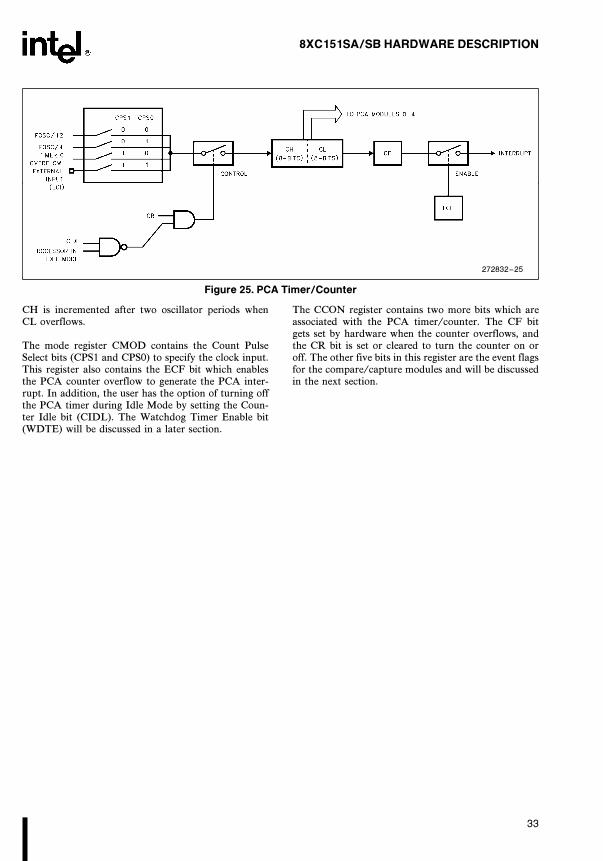
Figure 25. PCA Timer/Counter
CH is incremented after two oscillator periods whenCL overflows.
The mode register CMOD contains the Count PulseSelect bits (CPS1 and CPS0) to specify the clock input.This register also contains the ECF bit which enablesthe PCA counter overflow to generate the PCA inter-rupt. In addition, the user has the option of turning offthe PCA timer during Idle Mode by setting the Coun-ter Idle bit (CIDL). The Watchdog Timer Enable bit(WDTE) will be discussed in a later section.
The CCON register contains two more bits which areassociated with the PCA timer/counter. The CF bitgets set by hardware when the counter overflows, andthe CR bit is set or cleared to turn the counter on oroff. The other five bits in this register are the event flagsfor the compare/capture modules and will be discussedin the next section.
33

8XC151SA/SB HARDWARE DESCRIPTION
CMOD: PCA Counter Mode Register
CMOD Address: 0D9H
Reset State: 00XX X000B
Not Bit Addressable
7 0
CIDL WDTE Ð Ð Ð CPS1 CPS0 ECF
Symbol Function
CIDL Counter idle control: CIDL e 0 programs the PCA Counter to continue functioning duringidle Mode. CIDL e 1 programs it to be gated off during idle.
WDTE Watchdog Timer Enable: WDTE e 0 disables Watchdog Timer function on PCA Module 4.WDTE e 1 enables it.
Ð Not implemented, reserved for future use.*
CPS1 PCA Count Pulse Select bit 1.
CPS0 PCA Count Pulse Select bit 0.
CPS1 CPS0 Selected PCA Input**0 0 Internal clock, Fosc d 12
0 1 Internal clock, Fosc d 4
1 0 Timer 0 overflow
1 1 External clock at ECI/P1.2 pin (max. rate e Fosc d8)
ECF PCA Enable Counter Overflow interrupt: ECF e 1 enables CF bit in CCON to generate aninterrupt. ECF e 0 disables that function of CF.
NOTE:*User software should not write 1s to reserved bits. These bits may be used in future C151 family products to invokenew features. In that case, the reset or inactive value of the new bit will be 0, and its active value will be 1. The valueread from a reserved bit is indeterminate.**Fosc e oscillator frequency
6.2 Capture/Compare Modules
Each of the five compare/capture modules has six pos-sible functions it can perform:
Ð 16-bit Capture, positive-edge triggered
Ð 16-bit Capture, negative-edge triggered
Ð 16-bit Capture, both positive and negative-edgetriggered
Ð 16-bit Software Timer
Ð 16-bit High Speed Output
Ð 8-bit Pulse Width Modulator.
In addition, module 4 can be used as a Watchdog Tim-er. The modules can be programmed in any combina-tion of the different modes.
Each module has a mode register called CCAPMn(n e 0, 1, 2, 3, or 4) to select which function it willperform. Note the ECCFn bit which enables the PCAinterrupt when a module’s event flag is set. The eventflags (CCFn) are located in the CCON register and getset when a capture event, software timer, or high speedoutput event occurs for a given module.
34

8XC151SA/SB HARDWARE DESCRIPTION
CCON: PCA Counter Control Register
CCON Address: 0D8H
Reset State: 00X0 0000B
Bit Addressable
7 0
CF CR Ð CCF4 CCF3 CCF2 CCF1 CCF0
Symbol Function
CF PCA Counter Overflow flag. Set by hardware when the counter rolls over. CD flags aninterrupt if bit ECF in CMOD is set. CF may be set by either hardware or software but canonly be cleared by software.
CR PCA Counter Run control bit. Set by software to turn the PCA counter on. Must be clearedby software to turn the PCA counter off.
Ð Not implemented, reserved for future use.*
CCF4 PCA Module 4 interrupt flag. Set by hardware when a match or capture occurs. Must becleared by software.
CCF3 PCA Module 3 interrupt flag. Set by hardware when a match or capture occurs. Must becleared by software.
CCF2 PCA Module 2 interrupt flag. Set by hardware when a match or capture occurs. Must becleared by software.
CCF1 PCA Module 1 interrupt flag. Set by hardware when a match or capture occurs. Must becleared by software.
CCF0 PCA Module 0 interrupt flag. Set by hardware when a match or capture occurs. Must becleared by software.
NOTE:*User software should not write 1s to reserved bits. The value read from a reserved bit is indeterminate.
PCA Module Modes (CCAPMn Register) shows thecombinations of bits in the CCAPMn register that arevalid and have a defined function. Invalid combinationswill produce undefined results.
Each module also has a pair of 8-bit compare/captureregisters (CCAPnH and CCAPnL) associated with it.These registers store the time when a capture event oc-
curred or when a compare event should occur. For thePWM mode, the high byte regiser CCAPnH controlsthe duty cycle of the waveform.
The next five sections describe each of the compare/capture modes in detail.
35

8XC151SA/SB HARDWARE DESCRIPTION
CCAPMn: PCA Modules Compare/Capture Registers
CCAPMn Address CCAPM0: 0DAH
(n e 0–4) CCAPM1: 0DBH
CCAPM2: 0DCH
CCAPM3: 0DDH
CCAPM3: 0DEH
Reset State: X000 0000B
Not Bit Addressable
7 0
Ð ECOMn CAPPn CAPNn MATn TOGn PWMn ECCFn
Symbol Function
Ð Note implemented, reserved for future use.*
ECOMn Enable Comparator. ECOMn e 1 enables the comparator function.
CAPPn Capture Positive, CAPPn e 1 enables positive edge capture.
CAPNn Capture Negative, CAPNn e 1 enables negative edge capture.
MATn Match. When MATn e 1, a match of the PCA counter with this module’s compare/captureregister causes the CCFn bit in CCON to be set, flagging an interrupt.
TOGn Toggle. When TOGn e 1, a match of the PCA counter with this module’s compare/capture register causes the CEXn pin to toggle.
PWMn Pulse Width Modulation Mode. PWMn e 1 enables the CEXn pin to be used as a pulsewidth modulated output.
ECCFn Enable CCF Interrupt. Enables compare/capture flag CCFn in the CCON register togenerate an interrupt.
NOTE:*User software should not write 1s to reserved bits. The value read from a reserved bit is indeterminate.
PCA Module Modes (CCAPMn Register)
Ð ECOMn CAPPn CAPNn MATn TOGn PWMn ECCFn Module Function
X 0 0 0 0 0 0 0 No operation
X X 1 0 0 0 0 X 16-bit capture by a postive-edge trigger on CEXn
X X 0 1 0 0 0 X 16-bit capture by a negative-edge trigger on CEXn
X X 1 1 0 0 0 X 16-bit capture by a transition on CEXn
X 1 0 0 1 0 0 X 16-bit Software Timer
X 1 0 0 1 1 0 X 16-bit High Speed Output
X 1 0 0 0 0 1 0 8-bit PWM
X 1 0 0 1 x 0 x Watchdog Timer
X e Don’t Care
36

8XC151SA/SB HARDWARE DESCRIPTION
6.3 16-Bit Capture Mode
Both positive and negative transitions can trigger a cap-ture with the PCA. This gives the PCA the flexibility tomeasure periods, pulse widths, duty cycles, and phasedifferences on up to five separate inputs. Setting theCAPPn and/or CAPNn in the CCAPMn mode registerselect the input triggerÐpositive and/or negative tran-sitionÐfor module n. Refer to Figure 26.
The external input pins CEX0 through CEX4 are sam-pled for a transition. When a valid transition is detected(positive and/or negative edge), hardware loads the16-bit value of the PCA timer (CH, CL) into the mod-ule’s capture registers (CCAPnH, CCAPnL). The re-sulting value in the capture registers reflects the PCAtimer value at the time a transition was detected on theCEXn pin.
Upon a capture, the module’s event flag (CCFn) inCCON is set, and an interrupt is flagged if the ECCFnbit in the mode register CCAPMn is set. The PCA in-terrupt will then be generated if it is enabled. Since thehardware does not clear an event flag when the inter-rupt is vectored to, the flag must be cleared in software.
In the interrupt service routine, the 16-bit capture valuemust be saved in RAM before the next capture eventoccurs. A subsequent capture on the same CEXn pinwill write over the first capture value in CCAPnH andCCAPnL.
6.4 16-Bit Software Timer Mode
In the compare mode, the 16-bit value of the PCA tim-er is compared with a 16-bit value pre-loaded in themodule’s compare registers (CCAPnH, CCAPnL). Thecomparison occurs three times per machine cycle inorder to recognize the fastest possible clock input (i.e.(/4 x oscillator frequency). Setting the ECOMn bit inthe mode register CCAPMn enables the comparatorfunction as shown in Figure 27.
For the Software Timer mode, the MATn bit also needsto be set. When a match occurs between the PCA timerand the compare registers, a match signal is generatedand the module’s event flag (CCFn) is set. An interruptis then flagged if the ECCFn bit is set. The PCA inter-rupt is generated only if it has been properly enabled.Software must clear the event flag before the next inter-rupt will be flagged.
272832–26
n e 0, 1, 2, 3 or 4x e Don’t Care
Figure 26. PCA 16-Bit Capture Mode
37

8XC151SA/SB HARDWARE DESCRIPTION
During the interrupt routine, a new 16-bit compare val-ue can be written to the compare registers (CCAPnHand CCAPnL). Notice, however, that a write toCCAPnL clears the ECOMn bit which temporarily dis-ables the comparator function while these registers arebeing updated so an invalid match does not occur. Awrite to CCAPnH sets the ECOMn bit and re-enablesthe comparator. For this reason, user software shouldwrite to CCAPnL first, then CCAPnH.
6.5 High Speed Output Mode
The High Speed Output (HSO) mode toggles a CEXnpin when a match occurs between the PCA timer and apre-loaded value in a module’s compare registers. Forthis mode, the TOGn bit needs to be set in addition tothe ECOMn and MATn bits as seen in Figure 27. Bysetting or clearing the pin in software, the user canselect whether the CEXn pin will change from a logical0 to a logical 1 or vice versa. The user also has theoption of flagging an interrupt when a match event oc-curs by setting the ECCFn bit.
The HSO mode is more accurate than toggling portpins in software because the toggle occurs beforebranching to an interrupt. That is, interrupt latencywill not effect the accuracy of the output. If the userdoes not change the compare registers in an interruptroutine, the next toggle will occur when the PCA timerrolls over and matches the last compare value.
6.6 Watchdog Timer Mode
A Watchdog Timer is a circuit that automatically in-vokes a reset unless the system being watched sends
regular hold-off signals to the Watchdog. These circuitsare used in applications that are subject to electricalnoise, power glitches, electrostatic discharges, etc., orwhere high reliability is required.
The Watchdog Timer function is only available onPCA module 4. In this mode, every time the count inthe PCA timer matches the value stored in module 4’scompare registers, an internal reset is generated. (SeeFigure 28.) The bit that selects this mode is WDTE inthe CMOD register. Module 4 must be set up in eithercompare mode as a Software Timer or High Speed Out-put.
When the PCA Watchdog Timer times out, it resets thechip just like a hardware reset, except that it does notdrive the reset pin high.
To hold off the reset, the user has three options:
(1) periodically change the compare value so it willnever match the PCA timer,
(2) periodically change the PCA timer value so it willnever match the compare value,
(3) disable the Watchdog by clearing the WDTE bitbefore a match occurs and then later re-enable it.
The first two options are more reliable because theWatchdog Timer is never disabled as in option Ý3. Thesecond option is not recommended if other PCA mod-ules are being used since this timer is the time base forall five modules. Thus, in most applications the firstsolution is the best option.
If a Watchdog Timer is not needed, module 4 can stillbe used in other modes.
38

8XC151SA/SB HARDWARE DESCRIPTION
272832–27
n e 0, 1, 2, 3 or 4x e Don’t Care
Figure 27. PCA 16-Bit Comparator Mode: Software Timer and High Speed Output
6.7 Pulse Width Modulator Mode
Any or all of the five PCA modules can be pro-grammed to be a Pulse Width Modulator. The PWMoutput can be used to convert digital data to an analogsignal by simple external circuitry. The frequency of thePWM depends on the clock sources for the PCA timer.With a 16 MHz crystal the maximum frequency of thePWM waveform is 15.6 KHz.
The PCA generates 8-bit PWMs by comparing the lowbyte of the PCA timer (CL) with the low byte of themodule’s compare registers (CCAPnL). Refer to Figure29. When CL k CCAPnL the output is low. When CLt CCAPnL the output is high. The value in CCAPnLcontrols the duty cycle of the waveform. To change thevalue in CCAPnL without output glitches, the usermust write to the high byte register (CCAPnH). Thisvalue is then shifted by hardware into CCAPnL whenCL rolls over from 0FFH to 00H which corresponds tothe next period of the output.
39

8XC151SA/SB HARDWARE DESCRIPTION
272832–28
x e Don’t Care
Figure 28. Watchdog Timer Mode
272832–29
n e 0, 1, 2, 3 or 4x e Don’t Care
Figure 29. PCA 8-Bit PWM Mode
40

8XC151SA/SB HARDWARE DESCRIPTION
272832–30
Figure 30. CCAPnH Varies Duty Cycle
CCAPnH can contain any integer from 0 to 255 to varythe duty cycle from a 100% to 0.4% (see Figure 30).
7.0 SERIAL INTERFACE
The serial port is full duplex, meaning it can transmitand receive simultaneously. It is also receive-buffered,meaning it can commence reception of a second bytebefore a previously received byte has been read fromthe receive register. (However, if the first byte stillhasn’t been read by the time reception of the secondbyte is complete, one of the bytes will be lost). Theserial port receive and transmit registers are both ac-cessed through Special Function Register SBUF. Actu-ally, SBUF is two separate registers, a transmit bufferand a receive buffer. Writing to SBUF loads the trans-mit register, and reading SBUF accesses a physicallyseparate receive register.
The serial port control and status register is the SpecialFunction Register SCON. This register contains themode selection bits (SM0 and SM1); the SM2 bit for themultiprocessor modes (see Multiprocessor Communica-tions section); the Receive Enable bit (REN); the 9thdata bit for transmit and receive (TB8 and RB8); andthe serial port interrupt bits (TI and RI).
The serial port can operate in 4 modes:
Mode 0: Serial data enters and exits through RXD.TXD outputs the shift clock. 8 bits are transmitted/re-ceived: 8 data bits (LSB first). The baud rate is fixed at(/12 the oscillator frequency.
Mode 1: 10 bits are transmitted (through TXD) or re-ceived (through RXD): a start bit (0), 8 data bits (LSBfirst), and a stop bit (1). On receive, the stop bit goesinto RB8 in Special Function Register SCON. Thebaud rate is variable.
Mode 2: 11 bits are transmitted (through TXD) or re-ceived (through RXD): a start bit (0), 8 data bits (LSBfirst), a programmable 9th data bit, and a stop bit (1).Refer to Figure 31. On Transmit, the 9th data bit (TB8in SCON) can be assigned the value of 0 or 1. Or, forexample, the parity bit (P in the PSW) could be movedinto TB8. On receive, the 9th data bit goes into RB8 inSCON, while the stop bit is ignored. (The validity ofthe stop bit can be checked with Framing Error Detec-tion.) The baud rate is programmable to either (/32 or(/64 the oscillator frequency.
272832–31
Figure 31. Data Frame: Modes 1, 2 and 3
41

8XC151SA/SB HARDWARE DESCRIPTION
Mode 3: 11 bits are transmitted (through TXD) or re-ceived (through RXD): a start bit (0), 8 data bits (LSBfirst), a programmable 9th data bit and a stop bit (1). Infact, Mode 3 is the same as Mode 2 in all respectsexcept the baud rate. The baud rate in Mode 3 is vari-able.
In all four modes, transmission is initiated by any in-struction that uses SBUF as a destination register. Re-ception is initiated in Mode 0 by the condition RI e 0and REN e 1. Reception is initiated in the othermodes by the incoming start bit if REN e 1. For moredetailed information on each serial port mode, refer tothe ‘‘Hardware Description of the 8051, 8052, and80C51.’’
7.1 Framing Error Detection
Framing Error Detection allows the serial port to checkfor valid stop bits in modes 1, 2, or 3. A missing stop bitcan be caused, for example, by noise on the serial lines,or transmission by two CPUs simultaneously.
If a stop bit is missing, a Framing Error bit FE is set.The FE bit can be checked in software after each recep-tion to detect communication errors. Once set, the FEbit must be cleared in software. A valid stop bit will notclear FE.
The FE bit is located in SCON and shares the same bitaddress as SM0. Control bit SMOD0 in the PCON reg-ister determines whether the SM0 or FE bit is accessed.If SMOD0 e 0, then accesses to SCON.7 are to SM0.If SMOD0 e 1, then accesses to SCON.7 are to FE.
7.2 Multiprocessor Communications
Modes 2 and 3 provide a 9-bit mode to facilitate multi-processor communication. The 9th bit allows the con-troller to distinguish between address and data bytes.The 9th bit is set to 1 for address bytes and set to 0 fordata bytes. When receiving, the 9th bit goes into RB8 inSCON. When transmitting, TB8 is set or cleared insoftware.
The serial port can be programmed such that when thestop bit is received the serial port interrupt will be acti-vated only if the received byte is an address byte (RB8e 1). This feature is enabled by setting the SM2 bit inSCON. A way to use this feature in multiprocessor sys-tems is as follows.
When the master processor wants to transmit a block ofdata to one of several slaves, it first sends out an ad-dress byte which identifies the target slave. Remember,an address byte has its 9th bit set to 1, whereas a databyte has its 9th bit set to 0. All the slave processorsshould have their SM2 bits set to 1 so they will only beinterrupted by an address byte. In fact, the C151SX hasan Automatic Address Recognition feature which al-lows only the addressed slave to be interrupted. That is,the address comparison occurs in hardware, not soft-ware.
The addressed slave’s software then clears its SM2 bitand prepares to receive the data bytes that will be com-ing. The other slaves are unaffected by these data bytes.They are still waiting to be addressed since their SM2bits are all set.
7.3 Automatic Address Recognition
Automatic Address Recognition reduces the CPU timerequired to service the serial port. Since the CPU isonly interrupted when it receives its own address, thesoftware overhead to compare addresses is eliminated.With this feature enabled in one of the 9-bit modes, theReceive Interrupt (RI) flag will only get set when thereceived byte corresponds to either a Given or Broad-cast address.
The feature works the same way in the 8-bit mode(Mode 1) as in the 9-bit modes, except that the stop bittakes the place of the 9th data bit. If SM2 is set, the RIflag is set only if the received byte matches the Given orBroadcast Address and is terminated by a valid stopbit. Setting the SM2 bit has no effect in Mode 0.
The master can selectively communicate with groups ofslaves by using the Given Address. Addressing allslaves at once is possible with the Broadcast Address.These addresses are defined for each slave by two Spe-cial Function Registers: SADDR and SADEN.
A slave’s individual address is specified in SADDR.SADEN is a mask byte that defines don’t-cares to formthe Given Address. These don’t-cares allow flexibilityin the user-defined protocol to address one or moreslaves at a time. The following is an example of how theuser could define Given Addresses to selectively ad-dress different slaves.
42
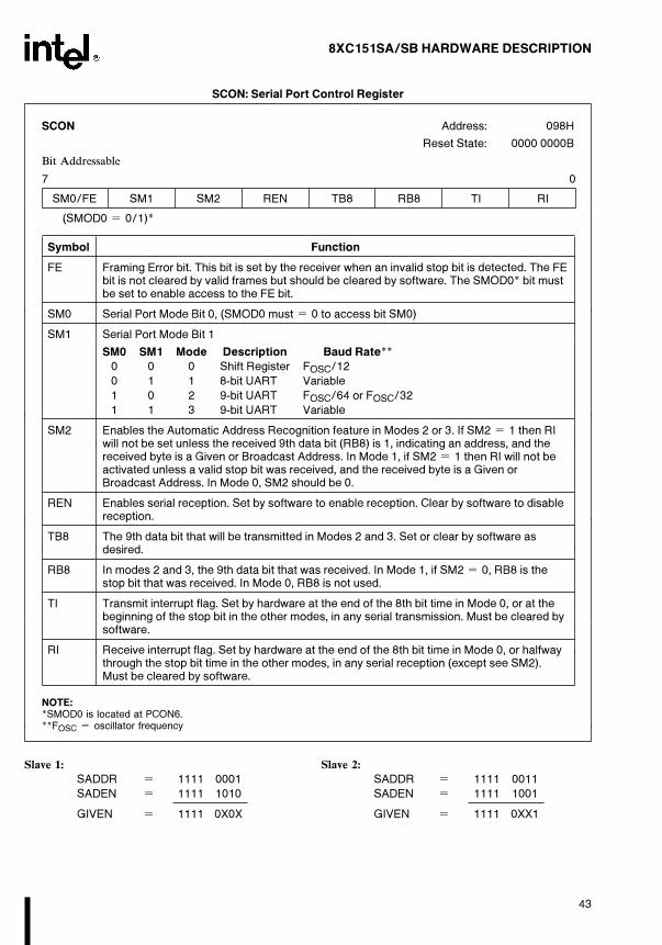
8XC151SA/SB HARDWARE DESCRIPTION
SCON: Serial Port Control Register
SCON Address: 098H
Reset State: 0000 0000B
Bit Addressable
7 0
SM0/FE SM1 SM2 REN TB8 RB8 TI RI
(SMOD0 e 0/1)*
Symbol Function
FE Framing Error bit. This bit is set by the receiver when an invalid stop bit is detected. The FEbit is not cleared by valid frames but should be cleared by software. The SMOD0* bit mustbe set to enable access to the FE bit.
SM0 Serial Port Mode Bit 0, (SMOD0 must e 0 to access bit SM0)
SM1 Serial Port Mode Bit 1
SM0 SM1 Mode Description Baud Rate**0 0 0 Shift Register FOSC/12
0 1 1 8-bit UART Variable
1 0 2 9-bit UART FOSC/64 or FOSC/32
1 1 3 9-bit UART Variable
SM2 Enables the Automatic Address Recognition feature in Modes 2 or 3. If SM2 e 1 then RIwill not be set unless the received 9th data bit (RB8) is 1, indicating an address, and thereceived byte is a Given or Broadcast Address. In Mode 1, if SM2 e 1 then RI will not beactivated unless a valid stop bit was received, and the received byte is a Given orBroadcast Address. In Mode 0, SM2 should be 0.
REN Enables serial reception. Set by software to enable reception. Clear by software to disablereception.
TB8 The 9th data bit that will be transmitted in Modes 2 and 3. Set or clear by software asdesired.
RB8 In modes 2 and 3, the 9th data bit that was received. In Mode 1, if SM2 e 0, RB8 is thestop bit that was received. In Mode 0, RB8 is not used.
TI Transmit interrupt flag. Set by hardware at the end of the 8th bit time in Mode 0, or at thebeginning of the stop bit in the other modes, in any serial transmission. Must be cleared bysoftware.
RI Receive interrupt flag. Set by hardware at the end of the 8th bit time in Mode 0, or halfwaythrough the stop bit time in the other modes, in any serial reception (except see SM2).Must be cleared by software.
NOTE:*SMOD0 is located at PCON6.**FOSC e oscillator frequency
Slave 1:
SADDR e 1111 0001
SADEN e 1111 1010
GIVEN e 1111 0X0X
Slave 2:
SADDR e 1111 0011
SADEN e 1111 1001
GIVEN e 1111 0XX1
43

8XC151SA/SB HARDWARE DESCRIPTION
The SADEN byte are selected such that each slave canbe addressed separately. Notice that bit 0 (LSB) is adon’t-care for Slave 1’s Given Address, but bit 1 e 1for Slave 2. Thus, to selectively communicate with justSlave 1 the master must send an address with bit 1 e 0(e.g. 1111 0000).
Similarly, bit 2 e 0 for Slave 1, but is a don’t-care forSlave 2. Now to communicate with just Slave 2 an ad-dress with bit 2 e 1 must be used (e.g. 1111 0111).
Finally, for a master to communicate with both slavesat once the address must have bit 1 e 1 and bit 2 e 0.
Notice, however, that bit 3 is a don’t-care for bothslaves. This allows two different addresses to selectboth slaves (1111 0001 or 1111 0101). If a third slavewas added that required its bit 3 e 0, then the latteraddress could be used to communicate with Slave 1 and2 but not Slave 3.
The master can also communicate with all slaves atonce with the Broadcast Address. It is formed from thelogical OR of the SADDR and SADEN registers withzeros defined as don’t-cares. The don’t-cares also allowflexibility in defining the Broadcast Address, but inmost applications a Broadcast Address will be 0FFH.
SADDR and SADEN are located at address A9H andB9H, respectively. On reset, the SADDR and SADENregisters are initialized to 00H which defines the Givenand Broadcast Addresses as XXXX XXXX (all don’t-cares). This assures the C151SX serial port to be back-wards compatibility with other MCSÉ-51 productswhich do not implement Automatic Addressing.
7.4 Baud Rates
The baud rate in Mode 0 is fixed:
Mode 0 Baud Rate e
Oscillator Frequency
12
The baud rate in Mode 2 depends on the value of bitSMOD1 in Special Function Register PCON. IfSMOD1 e 0 (which is the value on reset), the baudrate is (/64 the oscillator frequency. If SMOD1 e 1, thebaud rate is (/32 the oscillator frequency.
Mode 2 Baud Rate e 2SMOD1 c
Oscillator Frequency
64
The baud rates in Modes 1 and 3 are determined by theTimer 1 overflow rate, or by Timer 2 overflow rate, orby both (one for transmit and the other for receive).
7.5 Using Timer 1 to Generate BaudRates
When Timer 1 is used as the baud rate generator, thebaud rates in Modes 1 and 3 are determined by theTimer 1 overflow rate and the value of SMOD1 as fol-lows:
Modes 1 and 3Baud Rate
e 2SMOD1 c
Timer 1 Overflow Rate
32
Table 12. Timer 1 Generated Commonly Used Baud Rates
Timer 1
Baud Rate fOSC SMODC/TÝ Mode
Reload
Value
Mode 0 Max: 1 MHz 12 MHz X X X X
Mode 2 Max: 375K 12 MHz 1 X X X
Modes 1, 3: 62.5K 12 MHz 1 0 2 FFH
19.2K 11.059 MHz 1 0 2 FDH
9.6K 11.059 MHz 0 0 2 FDH
4.8K 11.059 MHz 0 0 2 FAH
2.4K 11.059 MHz 0 0 2 F4H
1.2K 11.059 MHz 0 0 2 E8H
137.5 11.986 MHz 0 0 2 1DH
110 6 MHz 0 0 2 72H
110 12 MHz 0 0 1 FEEBH
44

8XC151SA/SB HARDWARE DESCRIPTION
The Timer 1 interrupt should be disabled in this appli-cation. The Timer itself can be configured for either‘‘timer’’ or ‘‘counter’’ operation, and in any of its 3running modes. In most applications, it is configuredfor ‘‘timer’’ operation in the auto-reload mode (highnibble of TMOD e 0010B). In this case, the baud rateis given by the formula:
Modes 1 and 3Baud Rate
e
2SMOD1 c Oscillator Frequency
32 c 12 c [256 b (TH1)]
One can achieve very low baud rates with Timer 1 byleaving the Timer 1 interrupt enabled, and configuringthe Timer to run as a 16-bit timer (high nibble ofTMOD e 0001B), and using the Timer 1 interrupt todo a 16-bit software reload.
Table 12 lists various commonly used baud rates andhow they can be obtained from Timer 1.
7.6 Using Timer 2 to Generate BaudRates
Timer 2 is selected as the baud rate generator by settingTCLK and/or RCLK in T2CON (Table 11). Note thatthe baud rates for transmit and receive can be simulta-neously different. Setting RCLK and/or TCLK putsTimer 2 into its baud rate generator mode, as shown inFigure 32.
The baud rate generator mode is similar to the auto-re-load mode, in that a rollover in TH2 causes the Timer 2registers to be reloaded with the 16-bit value in registersRCAP2H and RCAP2L, which are preset by software.
The baud rates in Modes 1 and 3 are determined byTimer 2’s overflow rate as follows:
Modes 1 and 3 Baud Rates e
Timer 2 Overflow Rate
16
The Timer can be configured for either ‘‘timer’’ or‘‘counter’’ operation. In most applications, it is config-ured for ‘‘timer’’ operation (C/T2Ý e 0). The ‘‘Tim-er’’ operation is different for Timer 2 when it’s beingused as a baud rate generator. Normally, as a timer, itincrements every machine cycle ((/12 the oscillator fre-quency). As a baud rate generator, however, it incre-ments every state time ((/2 the oscillator frequency).The baud rate formula is given below:
Modes 1 and 3Baud Rate
e
Oscillator Frequency
32 c [65536 b (RCAP2H, RCAP2L)]
where (RCAP2H, RCAP2L) is the content ofRCAP2H and RCAP2L taken as a 16-bit unsignedinteger.
272832–32
Figure 32. Timer 2 in Baud Rate Generator Mode
45

8XC151SA/SB HARDWARE DESCRIPTION
Timer 2 as a baud rate generator is shown in Figure 32.This figure is valid only if RCLK and/or TCLK e 1 inT2CON. Note that a rollover in TH2 does not set TF2,and will not generate an interrupt. Therefore, the Timer2 interrupt does not have to be disabled when Timer 2is in the baud rate generator mode. Note too, that ifEXEN2 is set, a 1-to-0 transition in T2EX will setEXF2 but will not cause a reload from (RCAP2H,RCAP2L) to (TH2, TL2). Thus when Timer 2 is in useas a baud rate generator, T2EX can be used as an extraexternal interrupt, if desired.
It should be noted that when Timer 2 is running (TR2e 1) in ‘‘timer’’ function in the baud rate generatormode, one should not try to read or write TH2 or TL2.Under these conditions the Timer is being incrementedevery state time, and the results of a read or write maynot be accurate. The RCAP2 registers may be read, butshouldn’t be written to, because a write might overlap areload and cause write and/or reload errors. The timershould be turned off (clear TR2) before accessing theTimer 2 or RCAP2 registers.
Table 13 lists commonly used baud rates and how theycan be obtained from Timer 2.
Table 13. Timer 2 Generated
Commonly Used Baud Rates
Baud
Rate Freq
Osc Timer 2
RCAP2H RCAP2L
375K 12 MHz FF FF
9.6K 12 MHz FF D9
4.8K 12 MHz FF B2
2.4K 12 MHz FF 64
1.2K 12 MHz FE C8
300 12 MHz FB 1E
110 12 MHz F2 AF
300 6 MHz FD 8F
110 6 MHz F9 57
8.0 WATCHDOG TIMER
The C151SX contains a dedicated, hardware watchdogtimer (WDT) that automatically resets the chip if it isallowed to time out. The WDT provides a means ofrecovering from routines that do not complete success-fully due to software malfunctions. The WDT de-scribed in this section is not associated with the PCAwatchdog timer, which is implemented in software.
The WDT is a 14-bit counter that counts peripheralcycles, i.e. the system clock divided by twelve (FOSC/12). The WDTRST special function register at addressA6H provides control access to the WDT. Two opera-tions control the WDT:
# Device reset clears and disables the WDT
# Writing a specific two-byte sequence to theWDTRST register clears and enables the WDT.
If it is not cleared, the WDT overflows on count3FFFH a 1. With FOSC e 16 MHz, a peripheralcycle is 750 ns and the WDT overflows in 750 c 16384e 12.288 ms. The WDTRST is a write-only register.Attempts to read it return FFH. The WDT itself is notread or write accessible. The WDT does not drive theexternal RESET pin.
8.1 Using the WDT
To use the WDT to recover from software malfunc-tions, the user program should control the WDT asfollows:
1. Following device reset, write the two-byte sequence1EH–E1H to the WDTRST register to enable theWDT. The WDT begins counting from 0.
2. Repeatedly for the duration of program execution,write the two-byte sequence 1EH–E1H to theWDTRST register to clear and enable the WDT be-fore it overflows. The WDT starts over at 0.
If the WDT overflows, it initiates a device reset. Devicereset clears the WDT and disables it.
8.2 WDT During Idle Mode andPowerdown
Operation of the WDT during the power reductionmodes deserves special attention. The WDT continuesto count while the microcontroller is in idle mode. Thismeans the user must service the WDT during idle. Oneapproach is to use a peripheral timer to generate aninterrupt request when the timer overflows. The inter-rupt service routine then clears the WDT, reloads theperipheral timer for the next service period, and putsthe microcontroller back into idle.
The powerdown mode stops all phase clocks. This caus-es the WDT to stop counting and to hold its count. TheWDT resumes counting from where it left off if thepowerdown mode is terminated by INT0/INT1. To en-sure that the WDT does not overflow shortly after exit-ing the powerdown mode, clear the WDT just beforeentering powerdown. The WDT is cleared and disabledif the powerdown mode is terminated by a reset.
46

8XC151SA/SB HARDWARE DESCRIPTION
9.0 INTERRUPTS
Figure 33 illustrates the interrupt control system. TheC151SX has eight interrupt sources; seven maskablesources and the TRAP instruction (always enabled).The maskable sources include two external interrupts(INT0Ý and INT1Ý), three timer interrupts (timers 0,1, and 2), one programmable counter array (PCA) in-terrupt, amd one serial port interrupt. Each interrupt(except TRAP) has an interrupt request flag, which canbe set by software as well as by hardware. For someinterrupts, hardware clears the request flag when itgrants an interrupt. Software can clear any request flagto cancel an impending interrupt.
9.1 External Interrupts
External interrupts INT0Ý and INT1Ý (INTxÝ) pinsmay each be programmed to be level-triggered or edge-triggered, dependent upon bits IT0 and IT1 in theTCON register. If ITx e 0, INTxÝ is triggered by adetected low at the pin. If ITx e 1, INTxÝ is nega-tive-edge triggered. External interrupts are enabled
with bits EX0 and EX1 (EXx) in the IE0 register.Events on the external interrupt pins set the interruptrequest flags IEx in TCON. These request bits arecleared by hardware vectors to service routines only ifthe interrupt is negative-edge triggered. If the interrup-tis level-triggered, the interrupt service routine mustclear the request bit. External hardware must deassertINTxÝ before the service routine completes, or an ad-ditional interrupt is requested. External interrupt pinsmust be deasserted for at least four state times prior toa request.
External interrupt pins are sampled once every fourstate times (a frame length of 666.4 ns at 12 MHz). Alevel-triggered interrupt pin held low or high for anyfive-state time period guarantees detection. Edge-trig-gered external interrupts must hold the request pin lowfor at least five state times. This ensures edge recogni-tion and sets interrupt request bit EXx. The CPU clearsEXx automatically during service routine fetch cyclesfor edge-triggered interrupts.
47

8XC151SA/SB HARDWARE DESCRIPTION
272832–33
Figure 33. Interrupt Control System
48

8XC151SA/SB HARDWARE DESCRIPTION
Table 14. Interrupt Control Matrix
Interrupt NameGlobal
PCATimer Serial Timer
INT1ÝTimer
INT0ÝEnable 2 Port 1 0
Bit Name in IE0 EA EC ET2 ES ET1 EX1 ET0 EX0
Register
Interrupt Priority-
Within-LevelNA 7 6 5 4 3 2 1
(7 e Low Priority,
(1 e High Priority)
Bit Names in:
IPH0 Reserved IPH0.6 IPH0.5 IPH0.4 IPH0.3 IPH0.2 IPH0.1 IPH0.0
IPL0 Reserved IPL0.6 IPL0.5 IPL0.4 IPL0.3 IPL0.2 IPL0.1 IPL0.0
Programmable for
Negative-edgeNA Edge No No No Yes No Yes
Triggered or Level-
Triggered Detect?
Interrupt Request
Flag in CCON,NA
CF, TF2,RI, TI TF1 IE1 TF0 IE0
T2CON, SCON, or CCFx EXF2
TCON Register
Interrupt Request Edge Edge
Flag Cleared by No No No No Yes Yes, Yes Yes,
Hardware? Level No Level No
ISR Vector Address NA 0033H 002BH 0023H 001BH 0013H 000BH 0003H
9.2 Timer Interrupts
Two timer-interrupt request bits TF0 and TF1 (seeTCON register) are set by timer overflow (the excep-tion is Timer 0 in Mode 3). When a timer interrupt isgenerated, the bit is cleared by an on-chip-hardwarevector to an interrupt service routine. Timer interruptsare enabled by bits ET0, ET1, and ET2 in the IE0 regis-ter.
Timer 2 interrupts are generated by a logical OR of bitsTF2 and EXF2 in register T2CON. Neither flag iscleared by a hardware vector to a service routine. Infact, the interrupt service routine must determine ifTF2 or EXF2 generated the interrupt, and then clearthe bit. Timer 2 interrupt is enabled by ET2 in registerIE0.
49

8XC151SA/SB HARDWARE DESCRIPTION
9.3 Programmable Counter Array(PCA) Interrupt
The programmable counter array (PCA) interrupt isgenerated by logical OR of five event flags (CCFx) andthe PCA timer overflow flag (CF) in the CCON regis-ter. All PCA interrupts share a common interrupt vec-tor. Bits are not cleared by hardware vectors to serviceroutines. Normally, interrupt service routines resolveinterrupt requests and clear flag bits. This allows theuser to define the relative priorities of the five PCAinterrupts.
The PCA interrupt is enabled by bit EC in the IE0register. In addition, the CF flag and each of the CCFxflags must also be individually enabled by bits ECF andECCFx in registers CMOD and CCAPMx respectivelyfor the flag to generate an interrupt.
NOTE:
CCFx refers to 5 separate bits, one for eachPCA module (CCF0, CCF1, CCF2, CCF3,CCF4).CCAPMx refers to 5 separate registers, one foreach PCA module (CCAPM0, CCAPM1,CCAPM2, CCAPM3, CCAPM4).
9.4 Serial Port Interrupt
Serial port interrupts are generated by the logical OR ofbits RI and TI in the SCON register. Neither flag iscleared by a hardware vector to the service routine. Theservice routine resolves RI or TI interrupt generationand clears the serial port request flag. The serial portinterrupt is enabled by bit ES in the IE0 register.
9.5 Interrupt Enable
Each interrupt source (with the exception of TRAP)may be individually enabled or disabled by the appro-priate interrupt enable bit in the IE0 register. Note IE0also contains a global disable bit (EA). If EA is set,interrupts are individually enabled or disabled by bits inIE0. If EA is clear, all interrupts are disabled.
50

8XC151SA/SB HARDWARE DESCRIPTION
Interrupt Enable Register
IE0 Address: 0A8H
Reset State: 0000 0000B
7 0
EA EC ET2 ES ET1 EX1 ET0 EX0
BitFunction
Mnemonic
EA Global Interrupt Enable:
Setting this bit enables all interrupts that are individually enabled by bits 0–6. Clearingthis bit disables all interrupts, except the TRAP interrupt, which is always enabled.
EC PCA Interrupt Enable:
Setting this bit enables the PCA interrupt.
ET2 Timer 2 Overflow Interrupt Enable:
Setting this bit enables the timer 2 overflow interrupt.
ES Serial I/O Port Interrupt Enable:
Setting this bit enables the serial I/O port interrupt.
ET1 Timer 1 Overflow Interrupt Enable:
Setting this bit enables the timer 1 overflow interrupt.
EX1 External Interrupt 1 Enable:
Setting this bit enables external interrupt 1.
ET0 Timer 0 Overflow Interrupt Enable:
Setting this bit enables the timer 0 overflow interrupt.
EX0 External Interrupt 0 Enable:
Setting this bit enables external interrupt 0.
9.6 Interrupt Priorities
Each of the seven C151SX interrupt sources may beindividually programmed to one of four priority levels.This is accomplished with the IPH0.x/IPL0.x bit pairs
in the interrupt priority high (IPH0) and interrupt pri-ority low (IPL0) registers. Specify the priority level asshown in Table 15 using IPH0.x as the MSB andIPL0.x as the LSB.
51

8XC151SA/SB HARDWARE DESCRIPTION
Table 15. Level of Priority
IPH0.x (MSB) IPL0.x (LSB) Priority Level
0 0 0 Lowest Priority
0 1 1
1 0 2
1 1 3 Highest Priority
A low-priority interrupt is always interrupted by ahigher priority interrupt but not by another interrupt ofequal or lower priority. The highest priority interrupt isnot interrupted by any other interrupt source. Higherpriority interrupts are serviced before lower priority in-terrupts. The response to simultaneous occurrence ofequal priority interrupts (i.e., sampled within the samefour state interrupt cycle) is determined by a hardwarepriority-within-level resolver as shown in Table 16.
Table 16. Interrupt Priority Within Level
Priority Number * Interrupt Name
1 (Highest Priority) INT0Ý
2 Timer 0
3 INT1Ý
4 Timer 1
5 Serial Port
6 Timer 2
7 (Lowest Priority) PCA
* The C151SX interrupt priority-within-level table differsfrom MCSÉ 51 microcontrollers.
52
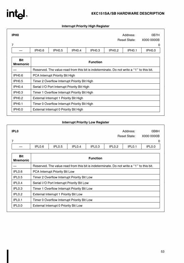
8XC151SA/SB HARDWARE DESCRIPTION
Interrupt Priority High Register
IPH0 Address: 0B7H
Reset State: X000 0000B
7 0
Ð IPH0.6 IPH0.5 IPH0.4 IPH0.3 IPH0.2 IPH0.1 IPH0.0
BitFunction
Mnemonic
Ð Reserved. The value read from this bit is indeterminate. Do not write a ‘‘1’’ to this bit.
IPH0.6 PCA Interrupt Priority Bit High
IPH0.5 Timer 2 Overflow Interrupt Priority Bit High
IPH0.4 Serial I/O Port Interrupt Priority Bit High
IPH0.3 Timer 1 Overflow Interrupt Priority Bit High
IPH0.2 External Interrupt 1 Priority Bit High
IPH0.1 Timer 0 Overflow Interrupt Priority Bit High
IPH0.0 External Interrupt 0 Priority Bit High
Interrupt Priority Low Register
IPL0 Address: 0B8H
Reset State: X000 0000B
7 0
Ð IPL0.6 IPL0.5 IPL0.4 IPL0.3 IPL0.2 IPL0.1 IPL0.0
BitFunction
Mnemonic
Ð Reserved. The value read from this bit is indeterminate. Do not write a ‘‘1’’ to this bit.
IPL0.6 PCA Interrupt Priority Bit Low
IPL0.5 Timer 2 Overflow Interrupt Priority Bit Low
IPL0.4 Serial I/O Port Interrupt Priority Bit Low
IPL0.3 Timer 1 Overflow Interrupt Priority Bit Low
IPL0.2 External Interrupt 1 Priority Bit Low
IPL0.1 Timer 0 Overflow Interrupt Priority Bit Low
IPL0.0 External Interrupt 0 Priority Bit Low
53

8XC151SA/SB HARDWARE DESCRIPTION
272832–34
Figure 34. The Interrupt Process
9.7 Interrupt Processing
Interrupt processing is a dynamic operation that beginswhen a source requests an interrupt and lasts until theexecution of the first instruction in the interrupt serviceroutine (see Figure 34). Response time is the amount oftime between the interrupt request and the resultingbreak in the current instruction stream. Latency is theamount of time between the interrupt request and theexecution of the first instruction in the interrupt serviceroutine. These periods are dynamic due to the presenceof both fixed-time sequences and several variable condi-tions. These conditions contribute to total elapsed time.
Both response time and latency begin with the request.The subsequent minimum fixed sequence comprises theinterrupt sample, poll, and request operations. Thevariables consist of (but are not limited to): specific in-structions in use at request time, internal versus exter-nal interrupt source requests, internal versus externalprogram operation, stack location, presense of waitstates, page-mode operation, and branch pointer length.
NOTE:
In the following discussion external interruptrequest pins are assumed to be inactive for atleast four state times prior to assertion. In thissection all external hardware signals maintainsome setup period (i.e., less than one statetime). Signals must meet VIH and VIL specifi-cations prior to any state time under discus-sion. This setup state time is not included inexamples or calculations for either response orlatency.
54

8XC151SA/SB HARDWARE DESCRIPTION
9.7.1 MINIMUM FIXED INTERRUPT TIME
All interrupts are sampled or polled every four statetimes (see Figure 34). Two of eight interrupts arelatched and polled per state time within any given four-state time window. One additional state time is requiredfor a context switch request. For code branches to jumplocations in the current 64-Kbyte memory region (com-patible with MCS 51 microcontrollers), the contextswitch time is 11 states. Therefore, the minimum fixedpoll and request time is 16 states (4 poll states a 1request state a 11 states for context switch e 16 statetimes).
Therefore, this minimum fixed period rests upon fourassumptions:
# The source request is an internal interrupt with highenough priority to take precedence over other poten-tial interrupts,
# The request is coincident with internal executionand needs no instruction completion time,
# The program uses an internal stack location, and
# The ISR is in on-chip OTPROM/ROM.
9.7.2 VARIABLE INTERRUPT PARAMETERS
Both response time and latency calculations containfixed and variable components. By definition, it is oftendifficult to predict exact timing calculations for real-time requests. One large variable is the completion timeof an instruction cycle coincident with the occurrenceof an interrupt request. Worst-case predictions typicallyuse the longest-executing instruction in an architec-ture’s code set.
9.7.3 RESPONSE TIME VARIABLES
Response time is defined as the start of a dynamic timeperiod when a source requests an interrupt and lastsuntil a break in the current instruction executionstream occurs (see Figure 34). Response time (andtherefore latency) is affected by two primary factors:the incidence of the request relative to the four-state-time sample window and the completion time of in-structions in the response period (i.e., shorter instruc-tions complete earlier than longer instructions).
NOTE:
External interrupt signals require one addition-al state time in comparison to internal inter-rupts. This is necessary to sample and latch thepin value prior to a poll of interrupts. The sam-ple occurs in the first half of the state time andthe poll/request occurs in the second half ofthe next state time. Therefore, this sample andpoll/request portion of the minimum fixed re-sponse and latency time is five states for inter-nal interrupts and six states for external inter-rupts. External interrupts must remain activefor at least five state times to guarantee inter-rupt recognition when the request occurs im-mediately after a sample has been taken (i.e.,requested in the second half of a sample statetime).
55

8XC151SA/SB HARDWARE DESCRIPTION
If the external interrupt goes active one state after thesample state, the pin is not resampled for another threestates. After the second sample is taken and the inter-rupt request is recognized, the interrupt controller re-quests the context switch. The programmer must alsoconsider the time to complete the instruction at themoment the context switch request is sent to the execu-tion unit. If 9 states of a 10-state instruction have com-pleted when the context switch is requested, the totalresponse time is 6 states, with a context switch immedi-ately after the final state of the 10-state instruction (seeFigure 35).
Conversely, if the external interrupt requests service inthe state just prior to the next sample, response is muchquicker. One state asserts the request, one state sam-ples, and one state requests the context switch. If atthat point the same instruction conditions exist, oneadditional state time is needed to complete the 10-stateinstruction prior to the context switch (see Figure 36).The total response time in this case is four state times.The programmer must evaluate all pertinent conditionsfor accurate predictability.
272832–35
Figure 35. Response Time Example Ý1
272832–36
Figure 36. Response Time Example Ý2
9.7.4 COMPUTATION OF WORST-CASELATENCY WITH VARIABLES
Worst-case latency calculations assume that the longestC151SX instruction used in the program must fully ex-ecute prior to a context switch. The instruction execu-tion time is reduced by one state with the assumptionthe instruction state overlaps the request state (there-fore, DIV is 10 state times b 1 e 9 states for latencycalculations). The calculations add fixed and variableinterrupt times to this instruction time to predict laten-cy. The worst-case latency (both fixed and variabletimes included) is expressed by a pseudo-formula:
FIXED TIME 0 VARIABLES 0LONGEST INSTRUCTION 4 MAXIMUM LATENCYPREDICTION
56
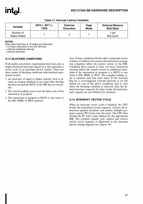
8XC151SA/SB HARDWARE DESCRIPTION
Table 17. Interrupt Latency Variables
VariableINT0Ý, INT1Ý, External Page External Memory
T2EX Execution Mode Wait State
Number of1 2 1
1 per
States Added Bus Cycle
NOTES:Base case fixed time is 16 states and assumes:ÐA 2-byte instruction is the first ISE byteÐInternal peripheral interruptÐInternal execution
9.7.5 BLOCKING CONDITIONS
If all enable and priority requirements have been met, asingle prioritized interrupt request at a time generates avector cycle to an interrupt service routine. There arethree causes of blocking conditions with hardware-gen-erated vectors:
1. An interrupt of equal or higher priority level is al-ready in progress (defined as any point after the flaghas been set and the RETI of the ISR has not execut-ed).
2. The current polling cycle is not the final cycle of theinstruction in progress.
3. The instruction in progress is RETI or any write tothe IE0, IPH0, or IPL0 registers.
Any of these conditions blocks calls to interrupt serviceroutines. Condition two ensures the instruction in prog-ress completes before the system vectors to the ISR.Condition three ensures at least one more instructionexecutes before the system vectors to additional inter-rupts if the instruction in progress is a RETI or anywrite to IE0, IPH0, or IPL0. The complete polling cy-cle is repeated each four state times. If the interruptflag for a level-triggered external interrupt is set butdenied for one of the above conditions and is clearwhen the blocking condition is removed, then the de-nied interrupt is ignored. In other words, blocked inter-rupt requests are not buffered for retention.
9.7.6 INTERRUPT VECTOR CYCLE
When an interrupt vector cycle is initiated, the CPUbreaks the instruction stream sequence, resolves all in-struction pipeline decisions, and pushes multiple pro-gram counter (PC) bytes onto the stack. The CPU thenreloads the PC with a start address for the appropriateISR. The complete sample, poll, request and contextswitch vector sequence is illustrated in the interruptlatency timing diagram (see Figure 34).
57

8XC151SA/SB HARDWARE DESCRIPTION
272832–37
Figure 37. External Clock Drive Waveforms
9.7.7 ISRS IN PROCESS
ISR execution proceeds until the RETI instruction isencountered. The RETI instruction informs the proces-sor the interrupt routine is completed. The RETI in-struction in the ISR pops PC address bytes off the stackand execution resumes at the suspended instructionstream.
With the exception of TRAP, the start addresses ofconsecutive interrupt service routines are eight bytesapart. If consecutive interrupts are used (IE0 and TF0,for example, or TF0 and IE1), the first interrupt rou-tine (if more than seven bytes long) must execute ajump to some other memory location. This preventsoverlap of the start address of the following interruptroutine.
For external clock drive requirements, see the devicedatasheet. Figure 37 shows the clock drive waveform.The external clock source must meet the minimumhigh and low times (TCHCX and TCLCX) and the maxi-mum rise and fall times (TCLCH and TCHCL) to mini-mize the effect of external noise on the clock generatorcircuit. Long rise and fall times increase the chance thatexternal noise will affect the clock circuitry and causeunreliable operation.
The external clock driver may encounter increased ca-pacitance loading at XTAL1 due to the Miller effect ofthe internal inverter as the clock waveform builds up inamplitude following power on. Once the input wave-form requirements are met, the input capacitance re-mains under 20 pF.
10.0 RESET
A device initializes the C151SX and vectors the CPU toaddress 0000H. A reset is required after applying powerat turn-on. A reset is a means of exiting the idle andpowerdown modes or recovering from software mal-functions.
To achieve a valid reset, VCC must be within its normaloperating range (see device datasheet) and the reset sig-nal must be maintained for 64 clock cycles (64 TOSC)after the oscillator has stabilized.
Device reset is initiated in two ways:
# externally, by asserting the RST pin
# internally, if the hardware WDT or the PCA WDTexpires
The power off flag (POF) in the PCON register indi-cates whether a reset is a warm start or a cold start. Acold start reset (POF e 1) is a reset that occurs afterpower has been off or VCC has fallen below 3V, so thecontents of volatile memory are indeterminate. POF isset by hardware when VCC rises from less than 3V toits normal operating level. A warm start reset (POF e
0) is a reset that occurs while the chip is at operatingvoltage, for example, a reset initiated by a WDT over-flow or an external reset used to terminate the idle orpower-down modes.
10.1 Externally Initiated Resets
To reset the C151SX, hold the RST pin at a logic highfor at least 64 clock cycles (64 TOSC) while the oscilla-tor is running. Reset can be accomplished automatical-ly at the time power is applied by capacitively couplingRST to VCC (see Figure 38). The RST pin has aSchmitt trigger input and a pulldown resistor.
58
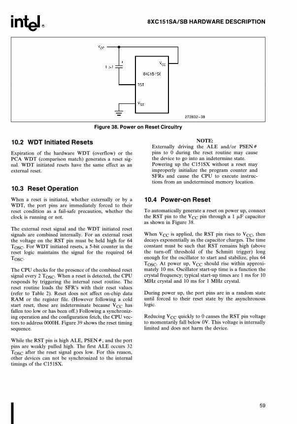
8XC151SA/SB HARDWARE DESCRIPTION
272832–38
Figure 38. Power on Reset Circuitry
10.2 WDT Initiated Resets
Expiration of the hardware WDT (overflow) or thePCA WDT (comparison match) generates a reset sig-nal. WDT initiated resets have the same effect as anexternal reset.
10.3 Reset Operation
When a reset is initiated, whether externally or by aWDT, the port pins are immediately forced to theirreset condition as a fail-safe precaution, whether theclock is running or not.
The external reset signal and the WDT initiated resetsignals are combined internally. For an external resetthe voltage on the RST pin must be held high for 64TOSC. For WDT initiated resets, a 5-bit counter in thereset logic maintains the signal for the required 64TOSC.
The CPU checks for the presence of the combined resetsignal every 2 TOSC. When a reset is detected, the CPUresponds by triggering the internal reset routine. Thereset routine loads the SFR’s with their reset values(refer to Table 2). Reset does not affect on-chip dataRAM or the register file. (However following a coldstart reset, these are indeterminate because VCC hasfallen too low or has been off.) Following a synchroniz-ing operation and the configuration fetch, the CPU vec-tors to address 0000H. Figure 39 shows the reset timingsequence.
While the RST pin is high ALE, PSENÝ, and the portpins are weakly pulled high. The first ALE occurs 32TOSC after the reset signal goes low. For this reason,other devices can not be synchronized to the internaltimings of the C151SX.
NOTE:
Externally driving the ALE and/or PSENÝpins to 0 during the reset routine may causethe device to go into an indetermine state.Powering up the C151SX without a reset mayimproperly initialize the program counter andSFRs and cause the CPU to execute instruc-tions from an undetermined memory location.
10.4 Power-on Reset
To automatically generate a reset on power up, connectthe RST pin to the VCC pin through a 1 mF capacitoras shown in Figure 38.
When VCC is applied, the RST pin rises to VCC, thendecays exponentially as the capacitor charges. The timeconstant must be such that RST remains high (abovethe turn-off threshold of the Schmitt trigger) longenough for the oscillator to start and stabilize, plus 64TOSC. At power up, VCC should rise within approxi-mately 10 ms. Oscillator start-up time is a function thecrystal frequency; typical start-up times are 1 ms for 10MHz crystal and 10 ms for 1 MHz crystal.
During power up, the port pins are in a random stateuntil forced to their reset state by the asynchronouslogic.
Reducing VCC quickly to 0 causes the RST pin voltageto momentarily fall below 0V. This voltage is internallylimited and does not harm the device.
59

8XC151SA/SB HARDWARE DESCRIPTION
272832–39
Figure 39. Reset Timing Sequence
11.0 POWER-SAVING MODES OFOPERATION
For applications where power consumption is critical,the C151SX provides two power reducing modes of op-eration: Idle and Power Down. The input throughwhich backup power is supplied during these opera-tions is VCC. Figure 40 shows the internal circuitrywhich implements these features. In the Idle mode(IDL e 1), the oscillator continues to run and the In-terrupt, Serial Port, PCA, and Timer blocks continueto be clocked, but the clock signal is gated off to theCPU. In Power Down (PD e 1), the oscillator is fro-zen. The Idle and Power Down modes are activated bysetting bits in Special Function Register PCON.
11.1 Idle Mode
An instruction that sets PCON.0 causes that to be thelast instruction executed before going into the Idlemode. In the Idle mode, the internal clock signal isgated off to the CPU, but not to the Interrupt, Timer,and Serial Port functions. The PCA can be pro-grammed either to pause or continue operating duringIdle (refer to the PCA section for more details). TheCPU status is preserved in its entirety: the Stack Point-
er, Program Counter, Program Status Word, Accumu-lator, and all other registers maintain their data duringIdle. The port pins hold the logical states they had atthe time Idle was activated. ALE and PSENÝ hold atlogic high levels.
There are two ways to terminate the Idle Mode. Activa-tion of any enabled interrupt will cause PCON.0 to becleared by hardware, terminating the Idle mode. Theinterrupt will be serviced, and following RETI the nextinstruction to be executed will be the one following theinstruction that put the device into Idle.
The flag bits (GF0 and GF1) can be used to give anindication if an interrupt occurred during normal oper-ation or during Idle. For example, an instruction thatactivates Idle can also set one or both flag bits. WhenIdle is terminated by an interrupt, the interrupt serviceroutine can examine the flag bits.
The other way of terminating the Idle mode is with ahardware reset.
The signal at the RST pin clears the IDL bit directlyand asynchronously. At this time the CPU resumesprogram execution from where it left off; that is, at theinstruction following the one that invoked the IdleMode.
60

8XC151SA/SB HARDWARE DESCRIPTION
272832–40
Figure 40. Idle and Power Down Hardware
PCON: Power Control Register
PCON Address: 087H
Reset State: 00XX 0000B
Not Bit Addressable
7 0
SMOD1 SMOD0 Ð POF GF1 GF0 PD IDL
Symbol Function
SMOD1 Double Baud rate bit. When set to a 1 and Timer 1 is used to generate baud rates, and theSerial Port is used in modes 1, 2, or 3.
SMOD0 When set, Read/Write accesses to SCON.7 are to the FE bit. When clear, Read/Writeaccesses to SCON.7 are to the SM0 bit.
Ð Not implemented, reserved for future use.*
POF Power Off Flag. Set by hardware on the rising edge of VCC. Set or cleared by software.This flag allows detection of a power failure caused reset. VCC must remain above 3V toretain this bit.
GF1 General-purpose flag bit.
GF0 General-purpose flag bit.
PD Power Down bit. Setting this bit activates Power Down operation.
IDL Idle mode bit. Setting this bit activates idle modes operation.
If 1s are written to PD and IDL at the same time, PD takes precedence.
NOTE:*User software should not write 1s to unimplemented bits. The value read from a reserved bit is indeterminate.
61

8XC151SA/SB HARDWARE DESCRIPTION
272832–41
Figure 41. Setup for Programming and Verifying Nonvolatile Memory
12.0 PROGRAMMING ANDVERIFYING NONVOLATILEMEMORY
The C151SX is programmed and verified in the samemanner as the 87C51FX, using same quick-pulse pro-gramming algorithm, which programs at VPP e
12.75V using a series of five 100 ms PROGÝ pulses perbyte. This results in a programming time of approxi-mately 16 seconds for the 16-Kbyte on-chip code mem-ory.
12.1 Programming and VerifyingModes
Table 18 lists the programming and verifying modesand provides details about the setup. The value appliedto port 0 determines the mode. The upper digit specifiesprogram or verify and the lower digit selects whatmemory function is programmed, i.e. on-chip codememory, encryption array, configuration bytes, etc.The addresses applied to port 1 and port 3 address loca-tions in the selected memory function. The encryption
array, lock bits, signature bytes reside in nonvolatilememory outside the memory address space. User con-figuration bytes (UCONFIG0 and UCONFIG1) residein nonvolatile memory at top of the memory addressspace for ROM/OTPROM devices and in externalmemory for devices without ROM/OTPROM.
The controller must be running with an oscillator fre-quency of 4 MHz to 6 MHz. To program, set up thecontroller as shown in Table 18 with the mode of oper-ation (program/verify and memory area) specified onport 0, the address with respect to the starting addressof the memory area applied to ports 1 and 3, and thedata on port 2. Apply a logic high to the RST pin andVCC to EAÝ/VPP. ALE/PSENÝ, normally an outputpin, must be held low externally.
To perform the write operation, raise VPP to 12.75Vand pulse the PROGÝ pin per Table 18. Then returnVPP to 5V. Verification is performed in a similar man-ner but without increasing VPP and without pulsingPROGÝ. The VPP source must be well regulated andfree of glitches. The voltage on the VPP pin must notexceed the specified maximum, even under transientconditions.
62
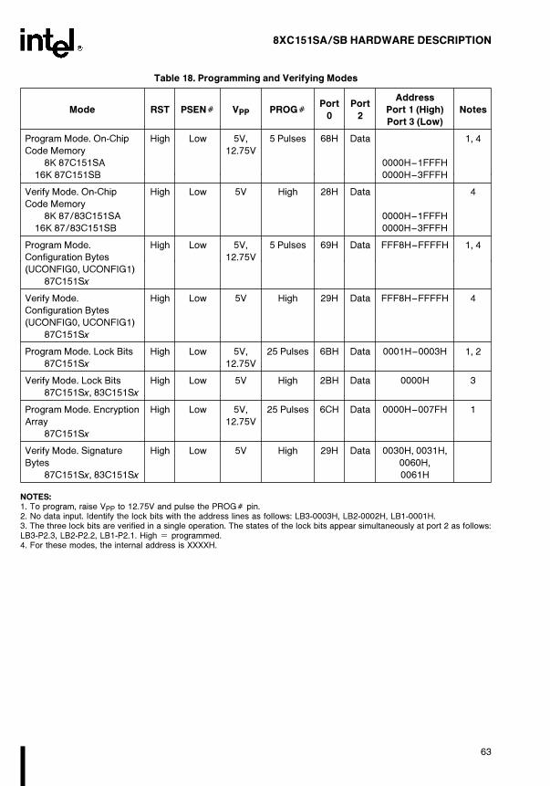
8XC151SA/SB HARDWARE DESCRIPTION
Table 18. Programming and Verifying Modes
Port PortAddress
Mode RST PSENÝ VPP PROGÝ0 2
Port 1 (High) Notes
Port 3 (Low)
Program Mode. On-Chip High Low 5V, 5 Pulses 68H Data 1, 4
Code Memory 12.75V
8K 87C151SA 0000H–1FFFH
16K 87C151SB 0000H–3FFFH
Verify Mode. On-Chip High Low 5V High 28H Data 4
Code Memory
8K 87/83C151SA 0000H–1FFFH
16K 87/83C151SB 0000H–3FFFH
Program Mode. High Low 5V, 5 Pulses 69H Data FFF8H–FFFFH 1, 4
Configuration Bytes 12.75V
(UCONFIG0, UCONFIG1)
87C151Sx
Verify Mode. High Low 5V High 29H Data FFF8H–FFFFH 4
Configuration Bytes
(UCONFIG0, UCONFIG1)
87C151Sx
Program Mode. Lock Bits High Low 5V, 25 Pulses 6BH Data 0001H–0003H 1, 2
87C151Sx 12.75V
Verify Mode. Lock Bits High Low 5V High 2BH Data 0000H 3
87C151Sx, 83C151Sx
Program Mode. Encryption High Low 5V, 25 Pulses 6CH Data 0000H–007FH 1
Array 12.75V
87C151Sx
Verify Mode. Signature High Low 5V High 29H Data 0030H, 0031H,
Bytes 0060H,
87C151Sx, 83C151Sx 0061H
NOTES:1. To program, raise VPP to 12.75V and pulse the PROGÝ pin.2. No data input. Identify the lock bits with the address lines as follows: LB3-0003H, LB2-0002H, LB1-0001H.3. The three lock bits are verified in a single operation. The states of the lock bits appear simultaneously at port 2 as follows:LB3-P2.3, LB2-P2.2, LB1-P2.1. High e programmed.4. For these modes, the internal address is XXXXH.
63

8XC151SA/SB HARDWARE DESCRIPTION
Table 19. Lock Bit Function
Lock Bits ProgrammedProtection Type
LB3 LB2 LB1
Level 1 U U U No program lock features are enabled. On-chip user code isencrypted when verified, if encryption array is programmed.
Level 2 U U P External code is prevented from fetching code bytes from on-chip code memory. Further programming of the on-chipOTPROM is disabled.
Level 3 U P P Same as level 2, plus on-chip code memory verify is disabled.
Level 4 P P P Same as level 3, plus external memory execution is disabled.
NOTE:Other combinations of the lock bits are not defined.
The C151SX stores configuration information in aneight-byte configuration array at FFF8H–FFFFH.UCONFIG0 (FFF8H) and UCONFIG1 (FFF9H) areimplemented; the remaining bytes are reserved for fu-ture use.
12.2 Lock Bit System
The 87C151SX provides a three-level lock system forprotecting user program code stored in the on-chipcode memory from unauthorized access. On the83151SX, only LB1 protection is available. Table 19describes the levels of protection.
12.3 Encryption Array
The 87C151SX and 83C151SX controllers include a128-byte encryption array located in nonvolatile memo-ry outside the memory address space. During verifica-tion of the on-chip code memory, the seven low-orderaddress bits also address the encryption array. As the
byte of the code memory is read, it is exclusive-NOR’ed(XNOR) with the key byte from the encryption array.If the encryption array is not programmed (still all 1s),the user program code is placed on the data bus in itsoriginal, unencrypted form. If the encryption array isprogrammed with key bytes, the user program code isencrypted and can’t be used without knowledge of thekey byte sequence. If the encryption feature is imple-mented, the portion of the on-chip code memory thatdoes not contain program code should be filled with‘‘random’’ byte values other than FFH to prevent theencryption key sequence from being revealed.
To preserve the secrecy of the encryption key byte se-quence, the encryption array can not be verified.
12.4 Signature Bytes
The C151SX contains factory-programmed signaturebytes. These bytes are located in nonvolatile memoryoutside the memory address space at 30H, 31H, and60H. Signature byte values are listed in Table 20.
64

8XC151SA/SB HARDWARE DESCRIPTION
Table 20. Contents of the Signature Bytes
ADDRESS CONTENTS DEVICE TYPE
30H 89H Indicates Intel Devices
31H 48H Indicates MCS 151 Core Product
60H 7BH Indicates 83C151SB Device
60H FBH Indicates 87C151SB Device
60H 7AH Indicates 83C151SA Device
60H FAH Indicates 87C151SA Device
13.0 ON-CIRCUIT EMULATION(ONCE) MODE
The on-circuit emulation (ONCE) mode permits exter-nal testers to test and debug C151SX based systemswithout removing the chip from the circuit board. Aclamp-on emulator or test CPU is used in place of theC151SX which is electrically isolated from the system.
To enter the ONCE mode:
1. Assert RST to initiate a device reset.
2. While holding RST asserted, apply and hold logiclevels to I/O pins as follows: PSENÝ e low, P0.7:5e low, P0.4 e high, P0.3:0 e low (i.e., port 0 e
10H).
3. Deassert RST, then remove the logic levels fromPSENÝ and port 0.
These actions cause the C151SX to enter the ONCEmode. Port 1, 2, and 3 pins are weakly pulled high andport 0, ALE, and PSENÝ pins are floating. Thus thedevice is electrically isolated from the remainder of thesystem which can then be tested by an emulator or testCPU. Note that in the ONCE mode the device oscilla-tor remains active.
65

8XC151SA/SB HARDWARE DESCRIPTION
14.0 ON-CHIP OSCILLATOR
This clock source uses an external quartz crystal con-nected from XTAL1 to XTAL2 as the frequency-deter-mining element (Figure 42). The crystal operates in itsfundamental mode as an inductive reactance in parallelresonance with capacitance external to the crystal. Os-cillator design considerations include crystal specifica-tions, operating temperature range, and parasitic boardcapacitance. Consult the crystal manufacturer’s data-sheet for parameter values. With high quality compo-nents, C1 e C2 e 30 pF is adequate for this applica-tion.
Pins XTAL1 and XTAL2 are protected by on-chipelectrostatic discharge (ESD) devices, D1 and D2,which are diodes parasitic to the RF FETs. They serveas clamps to VCC and VSS. Feedback resistor RF in theinverter circuit, formed from paralled n- and p- channelFETs, permits the PD bit in the PCON register to dis-able the clock during powerdown.
Noise spikes at XTAL1 and XTAL2 can disrupt micro-controller timing. To minimize coupling between otherdigital circuits and the oscillator, locate the crystal andthe capacitors near the chip and connect to XTAL1,XTAL2, and VSS with short, direct traces. To furtherreduce the effects of noise, place guard rings around theoscillator circuitry and ground the metal crystal case.
272832–42
Figure 42. CHMOS On-chip Oscillator
66
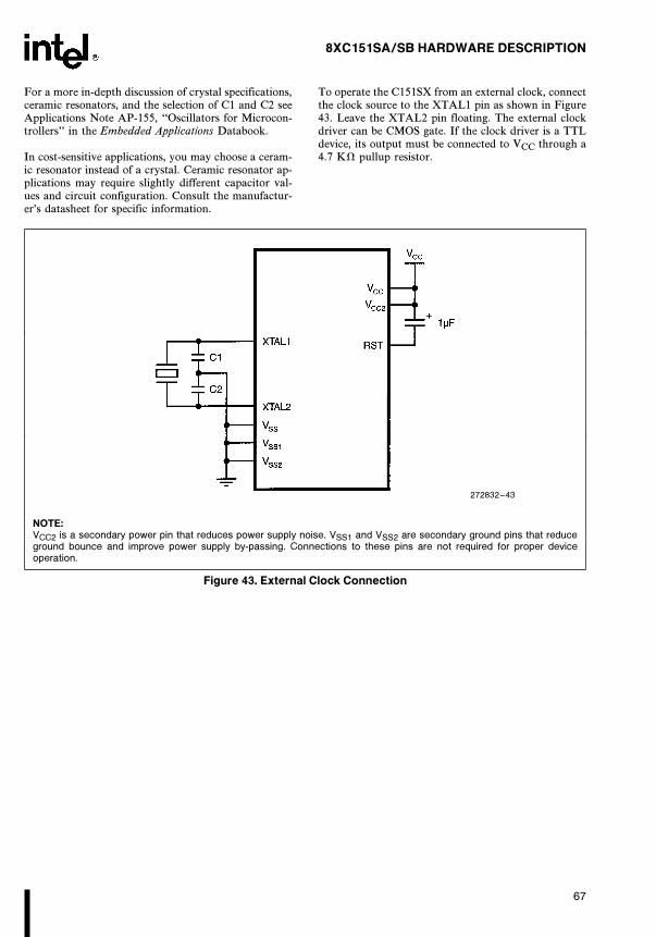
8XC151SA/SB HARDWARE DESCRIPTION
For a more in-depth discussion of crystal specifications,ceramic resonators, and the selection of C1 and C2 seeApplications Note AP-155, ‘‘Oscillators for Microcon-trollers’’ in the Embedded Applications Databook.
In cost-sensitive applications, you may choose a ceram-ic resonator instead of a crystal. Ceramic resonator ap-plications may require slightly different capacitor val-ues and circuit configuration. Consult the manufactur-er’s datasheet for specific information.
To operate the C151SX from an external clock, connectthe clock source to the XTAL1 pin as shown in Figure43. Leave the XTAL2 pin floating. The external clockdriver can be CMOS gate. If the clock driver is a TTLdevice, its output must be connected to VCC through a4.7 KX pullup resistor.
272832–43
NOTE:VCC2 is a secondary power pin that reduces power supply noise. VSS1 and VSS2 are secondary ground pins that reduceground bounce and improve power supply by-passing. Connections to these pins are not required for proper deviceoperation.
Figure 43. External Clock Connection
67

8XC151SA/SB HARDWARE DESCRIPTION
272832–44
Figure 44. External Clock Drive Waveforms
For external clock drive requirements, see the devicedatasheet. Figure 44 shows the clock drive waveform.The external clock source must meet the minimumhigh and low times (TCHCX and TCLCX) and the maxi-mum rise and fall times (TCLCH and TCHCL) to mini-mize the effect of external noise on the clock generatorcircuit. Long rise and fall times increase the chance thatexternal noise will affect the clock circuitry and causeunreliable operation.
The external clock driver may encounter increased ca-pacitance loading at XTAL1 due to the Miller effect ofthe internal inverter as the clock waveform builds up inamplitude following power on. Once the input wave-form requirements are met, the input capacitance re-mains under 20 pF.
ADDITIONAL REFERENCES
The following application notes provide supplementalinformation to this document and can be found in theEmbedded Applications Databook.
1. AP-125 ‘‘Designing Microcontroller Systems forElectrically Noisy Environments’’
2. AP-155 ‘‘Oscillators for Microcontrollers’’
3. 8XC151SA/SB Datasheet
4. 8XC251SA/SB/SP/SQ Datasheets
5. 8XC251SA/SB/SP/SQ User Manual
6. MCSÉ 51 Family User Manual
15.0 INSTRUCTION SET REFERENCETable 21. Summary of Add and Subtract Instructions
Add ADD kdestl,ksrcl dest opnd w dest cond a src opnd
Add with Carry ADDC kdestl,ksrcl (A) w (A) b src opnd a carry bit
Subtract with Borrow SUBB kdestl,ksrcl (A) w (A) b src opnd b carry bit
Mnemonic kdescl,ksrcl Notes Bytes States
ADD A, Rn Reg to Acc 1 1
A, Dir8 Dir Byte to Acc 2 1 (1)
A, @RI Indir Addr to Acc 1 2
A, Ýdata Immediate Data to Acc 2 1
ADDC; A, Rn Reg to/from Acc with Carry 1 1
SUBBA, Dir8 Dir Byte to/from Acc with Carry 2 1 (1)
A, @RI Indir RAM to/from Acc with Carry 1 2
A, Ýdata Immediate Data to/from Acc with Carry 2 1
NOTE:1. If this instruction addresses an I/O port (Px , x e 3:0), add 1 to the number of the states.
68

8XC151SA/SB HARDWARE DESCRIPTION
Table 22. Summary of Increment and Decrement Instructions
Increment INC DPTR (DPTR) w (DPTR) a 1
Increment INC byte byte w byte a 1
Increment INC kdestl,ksrcl dest opnd w dest opnd a src opnd
Decrement DEC byte byte w byte b 1
Mnemonic kdescl,ksrcl Notes Bytes States
INC; A Acc 1 1
DECRn Reg 1 1
Dir8 Dir Byte 2 2 (1)
@RI Indir RAM 1 3
INC DPTR Data Pointer 1 1
NOTE:1. If this instruction addresses an I/O port (Px , x e 0–3), add 2 to the number of the states.
Table 23. Summary of Multiply, Divide, and Decimal-adjust Instructions
Multiply MUL AB (B:A) e A c B
Divide DIV AB (A) e Quotient; (B) e Remainder
Decimal-adjust ACC DA A
for Addition (BCD)
Mnemonic kdescl,ksrcl Notes Bytes States
MUL AB Multiply A and B 1 5
DIV AB Divide A by B 1 10
DA A Decimal Adjust Acc 1 1
69

8XC151SA/SB HARDWARE DESCRIPTION
Table 24. Summary of Logical Instructions
Logical AND ANL kdestl,ksrcl dest opnd w dest opnd A src opnd
Logical OR ORL kdestl,ksrcl dest opnd w dest opnd V src opnd
Logical Exclusive OR XRL kdestl,ksrcl dest opnd w dest opnd V src opnd
Clear CLR A (A) w 0
Complement CPL A (AI) w O(AI)
Rotate RXX A (1)
SWAP A A3:0 Ý A7:4
Mnemonic kdescl,ksrcl Notes Bytes States
ANL; A, Rn Reg to Acc 1 1
ORL;A, Dir8 Dir Byte to Acc 2 1 (1)
XRLA, @RI Indir Addr to Acc 1 2
A, Ýdata Immediate Data to Acc 2 1
Dir8, A Acc to Dir Byte 2 2 (2)
Dir8, Ýdata Immediate Data to Dir Byte 3 3 (2)
CLR A Clear Acc 1 1
CPL A Complement Acc 1 1
RL A Rotate Acc Left 1 1
RLC A Rotate Acc Left Through the Carry 1 1
RR A Rotate Acc Right 1 1
RRC A Rotate Acc Right Through the Carry 1 1
SWAP A Swap Nibbles within the Acc 1 2
NOTES:1. If this instruction addresses an I/O port (Px , x e 0–3), add 1 to the number of the states.2. If this instruction addresses an I/O port (Px , x e 0–3), add 2 to the number of the states.
70

8XC151SA/SB HARDWARE DESCRIPTION
Table 25. Summary of Move Instructions
Move MOV kdestl,ksrcl destination w src opnd
Move Code Byte MOVC kdestl,ksrcl A w code byte
Move to External Mem MOVX kdestl,ksrcl external mem w (A)
Move from External Mem MOVX kdestl,ksrcl A w source opnd in external mem
Mnemonic kdescl,ksrcl Notes Bytes States
MOV A, Rn Reg to Acc 1 1
A, Dir8 Dir Byte to Acc 2 1 (1)
A, @RI Indir RAM to Acc 1 2
A, Ýdata Immediate Data to Acc 2 1
Rn, A Acc to Reg 1 1
Rn, Dir8 Dir Byte to Reg 2 1 (1)
Rn, Ýdata Immediate Data to Reg 2 1
Dir8, A Acc to Dir Byte 2 2 (1)
Dir8, Rn Reg to Dir Byte 2 2 (1)
Dir8, Dir8 Dir Byte to Dir Byte 3 3
Dir8, @RI Indir RAM to Dir Byte 2 3
Dir8, Ýdata Immediate Data to Dir Byte 3 3 (1)
@RI, A Acc to Indir RAM 1 3
@RI, Dir8 Dir Byte to Indir RAM 2 3
@RI, Ýdata Immediate Data to Indir RAM 2 3
DPTR, Ýdata16 Load Data Pointer with a 16-bit Const 3 2
MOVC A, @A a DPTR Code Byte Relative to DPTR to Acc 1 6
A, @A a PC Code Byte Relative to PC to Acc 1 6
MOVX A, @RI External Mem (8-bit Addr) to Acc 1 4
A, @DPTR External Mem (16-bit Addr) to Acc 1 5
@RI, A Acc to External Mem (8-bit Addr) 1 4
@DPTR, A Acc to External Mem (16-bit Addr) 1 5
NOTE:1. If this instruction addresses an I/O port (Px , x e 0–3), add 1 to the number of the states.
71

8XC151SA/SB HARDWARE DESCRIPTION
Table 26. Summary of Exchange, Push, and Pop Instructions
Exchange Contents XCH kdestl,ksrcl A Ý src opndExchange Digit XCH0 kdestl,ksrcl A3:0 Ý on-chip RAM bits 3:0Push PUSH ksrcl SP w SP a 1; (SP) w srcPop POP kdestl dest w (SP); SP w SP b 1
Mnemonic kdescl,ksrcl Notes Bytes States
XCH A, Rn Acc and Reg 1 3
A, DirB Acc and Dir Addr 2 3 (1)
A, @RI Acc and On-chip RAM (8-bit Addr) 1 4
XCHD A, @RI Acc and Low Nibble in On-chip RAM (8-bit Addr) 1 4
PUSH DirB Push Dir Byte onto Stack 2 2
POP Dir Pop Dir Byte from Stack 2 3/3
NOTE:1. If this instruction addresses an I/O port (Px , x e 0–3), add 2 to the number of the states.
Table 27. Summary of Bit Instructions
Clear Bit CLR bit bit w 0Set Bit SETB bit bit w 1Complement Bit CPL bit bit w ObitAND Carry with Bit ANL CY, /bit CY w CY ! bitAND Carry with Complement of Bit ANL CY, bit CY w CY ! ObitOR Carry with Bit ORL CY, bit CY w CY V bitOR Carry with Complement of Bit ORL CY, /bit CY w CY V ObitMove Bit to Carry MOV CY, bit CY w bitMove Bit from Carry MOV bit, CY bit w CY
Mnemonic kdescl,ksrcl Notes Bytes States
CLR CY Clear Carry 1 1
Bit51 Clear Dir Bit 2 2 (1)
SETB CY Set Carry 1 1
Bit51 Set Dir Bit 2 2 (1)
CPL CY Complement Carry 1 1
Bit51 Complement Dir Bit 2 2 (1)
ANL CY, Bit51 AND Dir Bit to Carry 2 1 (2)
ANL/ CY, /Bit51 AND Complemented Dir Bit to Carry 2 1 (2)
ORL CY, Bit51 OR Dir Bit to Carry 2 1 (2)
ORL/ CY, /Bit51 OR Complemented Dir Bit to Carry 2 1 (2)
MOV CY, Bit51 Move Dir Bit to Carry 2 1 (2)
Bit51, CY Move Carry to Dir Bit 2 2 (1)
NOTES:1. If this instruction addresses an I/O port (Px , x e 0–3), add 2 to the number of the states.2. If this instruction addresses an I/O port (Px , x e 0–3), add 1 to the number of the states.
72

8XC151SA/SB HARDWARE DESCRIPTION
Table 28. Summary of Control Instructions
Mnemonic kdescl,ksrcl Notes Bytes States (1)
ACALL Addr11 Absolute Subroutine Call 2 9
LCALL Addr16 Long Subroutine Call 3 9
RET Return from Subroutine 1 6
ERET Extended Subroutine Return 3 10
RETI Return from Interrupt 1 6
AJMP Addr11 Absolute Jump 2 3
LJMP Addr16 Long Jump 3 4
SJMP Rel Short Jump (Relative Addr) 2 3
JMP @A a DPTR Jump Indir Relative to the DPTR 1 5
JC Rel Jump if Carry is Set 2 1/4
JNC Rel Jump if Carry not Set 2 1/4
JB Bit51, Rel Jump if Dir Bit is Set 3 2/5
JNB Bit51, Rel Jump if Dir Bit is not Set 3 2/5
JBC Bit51, Rel Jump if Dir Bit is Set and Clear Bit 3 4/7
JZ Rel Jump if Acc is Zero 2 2/5
JNZ Rel Jump if Acc not Zero 2 2/5
CJNE A, Dir8, Rel Compare Dir Byte to Acc and Jump if not Equal 3 2/5
A, Ýdata, Rel Compare Immediate to Acc and Jump if not Equal 3 2/5
Rn, Ýdata, Rel Compare Immediate to Reg and Jump if not Equal 3 2/5
@RI, Ýdata, Rel Compare Immediate to Indir and Jump if not Equal 3 3/6
DJNZ Rn, rel Decrement Reg and Jump if not Zero 2 2/5
Dir8, Rel Decrement Dir Byte and Jump if not Zero 3 3/6
NOP Ð No Operation 1 1
NOTE:1. For conditional jumps, times are given as not-taken/taken.
73