922 ieee journal of solid-state circuits, vol. 42, no. 4
TRANSCRIPT

922 IEEE JOURNAL OF SOLID-STATE CIRCUITS, VOL. 42, NO. 4, APRIL 2007
Power and Area Minimization for MultidimensionalSignal Processing
Dejan Markovic, Member, IEEE, Borivoje Nikolic, Senior Member, IEEE, and Robert W. Brodersen, Fellow, IEEE
Abstract—Sensitivity-based methodology is applied to optimiza-tion of performance, power and area across several levels of designabstraction for a complex wireless baseband signal processing al-gorithm. The design framework is based on a unified, block-basedgraphical description of the algorithm to avoid design re-entryin various phases of chip development. The use of architecturaltechniques for minimization of power and area for complex signalprocessing algorithms is demonstrated using this framework. Asa proof of concept, an ASIC realization of the MIMO basebandsignal processing for a multi-antenna WLAN is described. Thechip implements a 4 4 adaptive singular value decomposition(SVD) algorithm with combined power and area minimizationachieving a power efficiency of 2.1 GOPS/mW (12-bit add equiv-alent) in just 3.5 mm2 in a standard 90 nm CMOS process. Thecomputational throughput of 70 GOPS is implemented with0.5 M cells at a 100 MHz clock and 385 mV supply, dissipating34 mW of power. With optimal channel conditions the algorithmimplemented can deliver up to 250 Mb/s over 16 sub-carriers.
Index Terms—Circuit optimization, CMOS digital integratedcircuits, design methodology, field-programmable gate arrays,matrix decomposition, MIMO systems, multidimensional signalprocessing, parallel architectures, pipelines, sensitivity.
I. INTRODUCTION
THE SCALING OF CMOS has been enabling integrationof higher complexity systems in each technology genera-
tion. Feature scaling by a factor of 0.7 doubles the density ofdigital logic. This benefit can be exploited in two ways: eitherto decrease the chip size (thus its cost) or to increase the amountof functionality while maintaining the same chip size. In wire-less and wireline communications applications the scaling oftechnology has traditionally been used for implementing moresophisticated signal processing in order to achieve higher datarates and better spectrum utilization.
Scaling of technology has imposed very tight power budgetsfor communications chips. Increased device leakages and de-creased rate of supply voltage scaling, along with the demandfor higher data rates and more functionality, have been steadilyincreasing the chip power consumption. Nowadays, powerconsumption of both fixed and mobile communication devicesis limited either by the heat dissipation and packaging, or by the
Manuscript received August 25, 2006; revised December 19, 2006. This workwas supported by C2S2 under MARCO Contract 2003-CT-888 and BWRCmember companies. Chip fabrication was provided by STMicroelectronics.
D. Markovic is with the Department of Electrical Engineering, University ofCalifornia, Los Angeles, CA 90095 USA (e-mail: [email protected]).
B. Nikolic and R. W. Brodersen are with the Berkeley Wireless ResearchCenter, University of California, Berkeley, CA 94704 USA.
Digital Object Identifier 10.1109/JSSC.2007.892191
battery life. The requirements for high data rate and increasedalgorithmic complexity in next-generation wireless devicespresent a difficulty for meeting the power budgets. Therefore,in designing next-generation wireless systems, algorithm de-signers, system architects and circuit designers face a challengeof how to optimally utilize the benefits of technology scaling ina short development cycle.
The problem that needs to be solved is complex: which al-gorithm optimally uses the underlying technology to achievethe desired data rate, while staying within the power and diesize limits? To answer this, every candidate algorithm has tobe mapped into an architecture that is optimal for a particulartechnology. The architecture choice strongly depends on the re-quired throughput, but also on the underlying technology op-tions, usually defined by the choice of supply and threshold volt-ages. Technologies with high off-state leakage “prefer” deeperpipelined architectures, while the technologies with less leakageprefer memory-oriented and highly parallel architectures. Tomeet the deployment targets, design teams will often settle to afirst architecture that meets the goals. Even when experimentingwith implementing multiple algorithms there is no proof of aclear advantage of one to another; the final choice is ultimatelydependent on a designer that achieves a smaller or lower powerimplementation with shorter design time.
At the lower level, problem of mapping architecture intosilicon can be formulated in many ways. Commonly, there isa required performance level, with acceptable power and areabudget. Since the performance of a communication system isoften dictated by the standard, small power or area are com-monly distinguishing features of a particular implementation.The overall design process, therefore, can be viewed as aconstrained optimization problem, where the power and/or areaare minimized under performance constraints.
This paper presents the methodology to formulate the systemdesign problem as a performance-constrained and area-con-strained power minimization. The problem will be solvedusing sensitivity-based optimization at multiple levels of de-sign abstraction. Design at higher abstraction layers providesmore room for power or area minimization then design at thecircuit-level. However, architectural optimization techniqueshave been largely heuristic, and there is no established sys-tematic way for trading off throughput, power and area. In ourapproach, optimal energy-delay tradeoffs from the circuit-levelare used to characterize multiple architectural realizations andthus guide architectural mapping for an algorithm.
Section II introduces multi-antenna signal processing fordecoupling of multi-path wireless channels, to demonstratethe level of complexity that can be supported with our design
0018-9200/$25.00 © 2007 IEEE

MARKOVIC et al.: POWER AND AREA MINIMIZATION FOR MULTIDIMENSIONAL SIGNAL PROCESSING 923
methodology. The methodology for algorithm-to-architecturemapping is described in Section III, including sensitivity basedoptimization framework, Simulink design description, andASIC design flow. The proposed approach enables power andarea optimizations across the boundary of algorithm, archi-tecture, and circuits, as presented in Section IV. Architecturalexploration of adaptive SVD algorithm is demonstrated inSection V. The power/area reduction concepts are experimen-tally validated as described in Section VII for an architectureoptimized for 0.4 V operation. Section VII concludes the paper.
II. MULTI-ANTENNA SIGNAL PROCESSING
The explosive growth of wireless communications, spurredby the availability of unlicensed spectrum bands, has fueled thedeployment of complex signal processing and coding schemesfor achieving higher data rates and more robust transmission.One direction in algorithms and systems research is in the useof MIMO systems to exploit degrees of freedom in the wirelesschannel and effectively increase its capacity. MIMO technologyhas been already adopted for use in next-generation WLANs.For example, to satisfy a growing need for higher capacity andextended range, OFDM-based WLAN devices [1] are moving tousing MIMO algorithms as being defined in the IEEE 802.11nstandard [2].
The computational requirements of baseband signal pro-cessing for MIMO algorithms are significantly higher thanthose of currently deployed systems. Ideally, a complete MIMOchannel decomposition would be performed independently ineach of the narrowband sub-carriers, which would producea computational increase that outstrips the improvementsprovided by scaling of technology alone. To illustrate the com-plexity, we select a multi-antenna algorithm that can deliver upto 250 Mb/s in 16 frequency sub-channels.
A. Multi-Path MIMO Channel
Multi-antenna technology can be used to improve robustnessor increase capacity of a wireless link [3]. Multiple antennashave traditionally been used as a method to overcome channelfading through increased diversity [4]. Link robustness is im-proved by multi-path averaging as shown in Fig. 1. By sendingthe same information over different paths and averaging overmultiple independently-faded replicas at the receiver, more reli-able communication is achieved. The number of averaging pathscan be artificially increased by sending the same signal overmultiple antennas. For example, if the transmitted signal is repli-cated over different paths, which correspond to transmit an-tennas, the average error probability decays as SNR as op-posed to SNR for the single-antenna case. Under these con-ditions, when the error probability decays as SNR , the di-versity gain is equal to [3]. Furthermore, having both mul-tiple transmit and multiple receive antennas improves the linkreliability by essentially averaging over multiple independently-faded paths. For a system with transmit and receive an-tennas, the maximum achievable diversity gain is .
Another potential of MIMO systems is increased capacity.The goal is to spatially localize transmission beams, so that inde-pendent data streams can be transmitted over multiple antennas
Fig. 1. Multi-path MIMO wireless channel increases robustness throughmulti-path averaging or increases capacity through spatial multiplexing. MIMOchannel is a complex matrix formed of transfer functions between individualantenna pairs.
for increased capacity. This method, known as spatial multi-plexing, takes advantage of fading by constructively combiningpaths that fade independently, which increases the degrees offreedom available for communication. The spatial-multiplexinggain can be quantified with the channel capacity increase. Fos-chini [4] showed that for an system, under certain channelconditions, the capacity of the channel increases linearly withthe number of spatial channels. The number of available spa-tial channels is the minimum between the number of transmitantennas and the number of receive antennas . In a MIMOsystem, channel is a complex matrix formed of transfer func-tions between individual antenna pairs. Vectors and in Fig. 1represent transmit and receive symbols, respectively. The goalis thus to estimate gains of the spatial sub-channels from and
information.MIMO channel decoding can be performed in several dif-
ferent ways. The pioneering work in MIMO decoding [4], [5]by Foschini resulted in formulation of Bell Labs Layered SpaceTime (BLAST) algorithms. In BLAST, codewords are arrangedin a space-time grid. The data is encoded over multiple transmitantennas and distributed in time. Depending on how the data isorganized in the space-time grid, there are diagonal [4] and ver-tical [5] architectures. Another approach to channel decodingis QR decomposition, which for a channel matrix is a fac-torization , where is a unitary matrix and isan upper triangular matrix. This method is traditionally usedto compute sub-spaces in various beam-forming algorithms [6].Full channel decoupling can be done using more computation-ally demanding methods such as singular value decomposition(SVD).
B. Singular Value Decomposition
Singular value decomposition is an optimal way to extractspatial multiplexing gains in MIMO channels [7]. Conceptof the SVD-based channel decoupling is illustrated in Fig. 2.Channel matrix can be represented as a product of , ,and , where and are unitary, and is a diagonal matrix.SVD can be also viewed as a composition of three operations:a rotation , a scaling operation , and another rotation
. When the channel matrix is partially known to thetransmitter, the optimal strategy is to transmit independentstreams in the directions of the eigenvectors of [3].Projection of modulated symbols onto matrix essentiallydirects the transmit symbols along eigen-modes of the fadingchannel. If the received signal is post-processed by rotating

924 IEEE JOURNAL OF SOLID-STATE CIRCUITS, VOL. 42, NO. 4, APRIL 2007
Fig. 2. Concept of singular value decomposition applied to MIMO channelmatrix H. The goal is to estimate gains of spatial MIMO channels, which aregiven by the ��� matrix.
Fig. 3. Adaptive blind-tracking SVD algorithm. Estimation of spatial channelgains is done at the receiver in the U� block.
along matrix, the channel between and appearsfully orthogonal. Then, independent data streams can be sentthrough the spatial sub-channels with gains correspondingto the entries in the matrix. At the receiver, data streamsarrive orthogonally without interference between the streams.The SVD matrices have to be adaptively estimated to tracktime-varying channel conditions.
Finding SVD of a channel matrix is a multidimensional signalprocessing task dealing with vector and matrix arithmetic. Thissort of computation involves hundreds of add and multiply op-erations, and may also need divide and square root. The overallcomplexity is well beyond the complexity of standard communi-cation blocks such as an FFT or a Viterbi decoder, so the choiceof architecture that minimizes power and area of the SVD be-comes an interesting question.
C. Adaptive Blind-Tracking SVD Algorithm
Fig. 3 is a block diagram of an adaptive blind-tracking SVDalgorithm proposed by Poon [8]. The core of the algorithm is inthe and V blocks, which estimate corresponding matrices.Hat symbol is used to indicate estimates. Channel decou-pling is done at the receiver. As long as there is a sizable numberof received symbols within a fraction of the coherence time,the receiver can estimate and from the received data alone.Tracking of the matrix is based on decision-directed estimatesof the transmitted symbols . matrix is periodically sent to thetransmitter through the feedback channel.
MIMO decoder specifications for the chip we implementedare derived from the following system: 4 4 antenna systemwith variable-constellation PSK modulation, 16 MHz ofchannel bandwidth utilized by 16 sub-carriers (correspondingto the narrowband frequency sub-channels). The chip presentedin this paper integrates the algorithm and rotation along
matrix, which is over 80% of complexity of the entire SVD.Back-channel information about the matrix is used at the
Fig. 4. LMS-based estimation of gains in spatial channels. The arithmetic com-plexity is about 300 adders, 400 multipliers, and 8 square roots and dividers.This level of complexity is hard to optimize in RTL.
transmitter, so integration of the tracking algorithm wouldbe required in the complete system realization.
The block performs sequential estimation of the eigen-pairs, eigenvectors and eigenvalues, using the adaptive MMSE-based algorithm from [8]. Traditionally, this kind of tracking isdone by evaluating the eigen-pairs of the autocorrelation ma-trix. The algorithm shown in Fig. 4 reduces matrix arithmeticto vector-based arithmetic with additional square root and divi-sion, which greatly reduces computational complexity. Estima-tion of eigen-pairs starts by finding the dominant eigenvalue ,using the full rank information . The LMS recursive al-gorithm in Fig. 4 estimates , which is the product of the eigen-vector and the eigenvalue . Each symbol period, complexvector is updated with the LMS correction factor. Based on
, the algorithm computes and . Then, the projection ofon the direction of the tracked dominant eigenvector is removed,and the algorithm is applied on the residue to track the seconddominant eigen-mode. The cancellation and tracking processproceeds until all eigen-pairs are estimated. Step-size is adap-tively adjusted based on the estimated eigenvalues. The squareroot and division are implemented using Newton–Rhapson iter-ative formulas, which have quadratic convergence [9]. In imple-mentation terms, this means that each iteration resolves two bitsof accuracy [10]. Under slowly varying input, which is the casewith MIMO channel data, the result can be taken as the initialcondition for the next iteration to obtain the answer in a singleiteration.
Computational complexity of the algorithm can be inferredfrom formulas in Fig. 4 by decomposing complex-valued vectoroperands into equivalent real-valued scalar operands. Overall,the algorithm requires about 300 adders, 400 multipliers, and8 square roots and dividers. Additionally, the operations are dis-tributed around nested feedback loops due to recursive nature ofthe algorithm.
III. DESIGN METHODOLOGY
The design methodology is based on balancing sensitivitiesat multiple levels of design description. Basic building blocks,such as adders and multipliers are characterized at circuit-levelfor power and delay, over varying wordlenghts and switchingactivities. The algorithm is mapped to architecture in a top-downprocess, with physical-level data mapped back into a high-leveldesign description. An energy and area optimal mapping of an

MARKOVIC et al.: POWER AND AREA MINIMIZATION FOR MULTIDIMENSIONAL SIGNAL PROCESSING 925
Fig. 5. Sensitivity-based optimization. Energy-delay sensitivity is the slope oftuning each variable in the energy-delay space. The highest energy efficiency isachieved by equalizing sensitivity to all variables.
algorithm into architecture and a circuit with a required perfor-mance is achieved when all energy-performance and area-per-formance sensitivities for various blocks in the same level ofhierarchy as well as across different levels of hierarchy are bal-anced.
The high-level design description is created in Simulink. Thesame description is used for functional simulation, rapid systemevaluation on an FPGA array, and ASIC synthesis. This unifieddesign description also allows for a seamless FPGA-assistedverification of the fabricated ASIC. The design infrastructureenables large design space exploration including algorithms, ar-chitectures, and circuits, thus enabling for optimization acrossvarious abstraction layers.
A. Sensitivity-Based Optimization Framework
The goal of mapping of an algorithm into architecture isto achieve minimum energy under performance and area con-straints. The plot in Fig. 5 illustrates energy-delay sensitivity,which is simply the slope of a curve in the energy-delay spacethat corresponds to tuning of a circuit-level design variable.The variables at the circuit-level can be gate sizes, transistorthresholds and supply voltages, while they can correspond tologic depth at a higher level. The most energy-efficient designis achieved when the sensitivities to all variables are equal, orwhen the variables reach their limits [11]. Similarly, the mostarea-efficient design is achieved when the area-performancesensitivities are balanced. Area optimization for dedicated DSPalgorithms differs from the optimization for microprocessors[12], [13].
The results from [11] were obtained on simple datapathblocks, using continuous tuning of transistor sizes, supply andthreshold voltage. It has been demonstrated that 65% of energycan be saved without delay penalty or, equivalently, the delaycan be improved by 25% without energy increase, comparedto the design sized for minimum delay at nominal and
. In this work, we demonstrate large energy savings on acomplex design using the same principles of optimization withsmall changes in a conventional ASIC design methodology.
The key observations from prior work [11] are used as guide-lines for the ASIC design: 1) gate sizing is the most effective inreducing the energy near (up to 20%) the minimum delay point;2) voltage scaling is the most effective for large incremental de-lays; and 3) threshold adjustment is the least effective due tobroad energy minimum as a function of leakage-to-switchingratio. In order to apply the sensitivity-based optimization on a
hierarchical, complex design, these principles are applied to atiming-driven logic synthesis with discrete gate sizes.
B. Block Characterization
Circuit-level characterization augments basic design libraryblocks with technology-dependent information for power,speed, and area, thus providing complete information forblock-based architecture design. Basic primitives includesimple operators such as add, multiply, shift, mux, register andso on, so a full characterization over a range of latency andword-size parameters is possible. The logic depth is chosensuch that the registers are inserted between these logic primi-tives when composing a larger function.
Plot in Fig. 6(a) shows typical curves for add and multiplyblocks, for a fixed number of bits, where all points on the curvesare characterized for power and area. For a range of interest, theslope of the E–D curves as a function of logic depth for addersand multipliers are similar, and can be matched to the sensitivityto lower-level parameters (supply and sizing). The difference ingate complexity of these blocks translates into different laten-cies of their implementations, for the equal cycle time.
Concept of balancing sensitivity to supply and gatesize is graphically illustrated in Fig. 6(b). Design sized forminimum delay at nominal supply has very large sensitivity togate sizing. The sensitivity to and is balanced by down-sizing the logic, which results in some delay increase. Asscales down to reach the target delay, has to adjust to trackreduced sensitivity to . Combining results of energy-delayand latency versus cycle time characterization provides insightinto optimal supply voltage, gate size, and logic depth .Pipeline balancing at the block level thus enables hierarchicalexpansion for full algorithm realization.
C. Simulink Design Environment
Design re-entry in various phases of system development isa standard practice today. A design is entered in various formsby different designers or different teams, resulting in heteroge-neous design descriptions. Algorithm developers tend to workin C or Matlab environment, which has an array of built-in func-tions convenient for quick algorithm modeling and verification.SystemC [14] is another behavioral entry, closer to traditionalhardware descriptions like Verilog or VHDL, but requires moresophisticated programming skills. The architectural descriptionis then created separately by hardware designers who have tocompletely re-enter the design in a hardware description lan-guage (HDL). This dramatically limits the possibility of ex-ploring various architectures for a given algorithm or modifyingthe algorithm to better map onto the underlying technology.
We use unified graphical Simulink design environment[15], which is widely adopted by algorithm developers. Analgorithm is entered only once is a graphical block form, thateasily maps onto a corresponding dataflow architecture. Thisapproach enables algorithm verification or hardware emulation,and also provides abstract view of design architecture, therebyavoiding costly design re-entry. The methodology relies ontimed-dataflow block-level representation of an algorithm.Fixed-point block set includes basic operators such as add,

926 IEEE JOURNAL OF SOLID-STATE CIRCUITS, VOL. 42, NO. 4, APRIL 2007
Fig. 6. Block characterization methodology. (a) Block library is augmented with information for speed, power, and area, in addition to existing wordlength andlatency parameters. (b) Latency versus cycle time for a block is characterized over a range of supply voltages. Optimal logic depth (L ), supply (V ) and gatesize (W ) for a block is determined.
multiply, shift, mux, and so on with notion of hardware pa-rameters such as finite wordlength and latency. This is thelevel of abstraction we work with to efficiently optimize thearchitecture.
D. FPGA-Assisted ASIC Design Flow
Design cycle includes algorithm modeling, design optimiza-tions, and final ASIC verification, all carried out using Simulinkenvironment. Once the bit-true, cycle-accurate behavior is es-tablished, the Simulink description of the block interconnects isused to generate the hardware description for mapping the de-sign onto a FPGA array. The same description is also used as anentry into the ASIC tool flow.
The ASIC flow shown in Fig. 7 takes block-level connectivityfrom Simulink and generates HDL for chip synthesis using anin-house tool [16]. The tool builds scripts to synthesize basicprimitives and allows constraints to be passed to synthesis toimprove compilation results. The tool also does first synthesisto map the complete design to the gate level, and HDL simula-tion to verify functional equivalence between the two hardwaredescriptions, using test vectors from Simulink. The synthesizednetlist is then optimized using a set of custom scripts for reg-ister retiming and logic optimization, before going to the finalstage of physical layout synthesis. With technology-dependentcharacterization of basic blocks for speed, power, and area, thearchitecture can be also optimized in Simulink, without the needfor excessive iterations through the design flow.
IV. ALGORITHM–ARCHITECTURE–CIRCUIT CO-DESIGN
Design environment presented in Section III is used to eval-uate various architectural techniques in the energy-area-perfor-mance space. Prior work evaluated the impact of circuit-leveldecisions such as gate sizing and circuit topology on various FIRfilter architectures [17], based on gate size characterization in astandard VLSI synthesis environment. The unified methodologypresented in this paper encompasses more degrees of freedomin the design and is scalable to complex designs.
Fig. 7. ASIC design flow. In-house tool generates HDL for chip synthesisbased on the FPGA Simulink design entry. The ASIC flow maintains func-tional equivalency with the FPGA flow to allow FPGA-based ASIC test. Thearchitecture is optimized in Simulink based on architectural feedback (speed,power, area) from synthesis.
A. Wordlength Optimization
The first step in the design optimization is wordlength re-duction, which is done using FFC, a custom floating-to-fixedpoint conversion tool [18]. The objective is to minimize hard-ware utilization subject to user specified mean-square quantiza-tion error.
The use of FFC is illustrated in Fig. 8. An FFC spec-markerdefines the mean-square error (MSE) specification for desirednodes in the system, typically output, while the hardwarecost estimation block calculates FPGA hardware utilizationin terms of FPGA slices, flip-flops, and look-up tables. Afterthe MSE constraints have been formulated, the FFC tool runsa number of simulations to calculate wordlength sensitivitiesand applies perturbation theory [19] to find the optimal result.Integer bits are determined based on input data dependentrange detection. The optimization is performed hierarchically,to relax the memory requirements and reduce the simulationtime. The tool can also append some guard bits in order to

MARKOVIC et al.: POWER AND AREA MINIMIZATION FOR MULTIDIMENSIONAL SIGNAL PROCESSING 927
Fig. 8. Simulink model of a MIMO transceiver used to evaluate the SVD algorithm. Optimal top-level wordlengths are indicated, the numbers are (total, fractional)bits.
avoid long simulation times. A detailed description of the toolwith examples and a user tutorial can be found in [20].
B. Architectural Transformations
Architectural transformations, such as pipelining, paral-lelism, time-multiplexing and folding are applied successivelyto a bit-true, cycle-accurate Simulink model to minimize powerand area under throughput/latency constraints. Impact of indi-vidual transformations on the overall chip characteristics highlydepends on the circuit-level performance.
1) Parallelism and Pipelining: The concepts of parallelismand pipelining (Fig. 9) are well-known in architecture design[21], [22]. Parallelism distributes computation over severalparallel branches, while pipelining inserts pipeline registersbetween logic blocks. When combined with adjustment insupply voltage, both techniques reduce the energy by relaxingthe delay of the datapath logic (blocks and in Fig. 9). Thearea-energy-delay plane in Fig. 9 shows energy-delay tradeoffin the logic blocks, and the area of corresponding architec-ture. Starting from the reference architecture, parallelism andpipelining relax the delay constraint to reduce energy at theexpense of increased area (shaded blocks). Alternatively, withconstant clock frequencies, parallelism and pipelining trade offthe increase in area for higher throughputs.
2) Time-Multiplexing: Time-multiplexing is another com-monly used architectural technique. The concept is illustratedin Fig. 10 on an example of a datapath, where block is somelogic function that evaluates multiple incoming streams of data.Time-multiplexing reduces the area through resource sharing,but needs a higher clock rate and thus higher supply voltageto maintain the throughput, as shown in the area-energy-delayplane in Fig. 10. Alternatively, time-multiplexing can lower thethroughput by maintaining the clock rate.
3) Data-Stream Interleaving: Data-stream interleaving is amajor technique for area reduction in multidimensional signalprocessing. Recursive operation is the underlying principle inthe LMS-based tracking of eigen-modes, so simple case is ex-amined in Fig. 11 to illustrate the concept. Top diagram illus-trates block-level representation of the recursive operation on
Fig. 9. Parallelism and pipelining increase delay of the underlying logic blocksand reduce energy through voltage scaling. Area of the resulting implementationincreases.
Fig. 10. Time multiplexing reduces delay of the underlying logic blocks andincreases energy through increase in supply voltage. Area of the resulting im-plementation decreases.
the right. The output sample is a sum of a current inputand a delayed and scaled version of a previous output. Clockfrequency corresponds to the sample time. Simple model

928 IEEE JOURNAL OF SOLID-STATE CIRCUITS, VOL. 42, NO. 4, APRIL 2007
Fig. 11. Data-stream interleaving. Independent streams of data are up-sampledand time-interleaved to maximize resource sharing for reduced area.
Fig. 12. Folding allows resource sharing in serially ordered signal processing.Alg block performs a recursive operation and needs deeper pipelining to supportfolding. The example illustrates folding of the U� algorithm from Fig. 4.
shown in the top diagram assumes zero latency of the add andmultiply blocks. The model is refined by adding appropriate la-tency at the output of the add and multiply blocks, re-spectively, as shown in the bottom diagram. This creates anopportunity to interleave multiple streams of data and reducearea compared to the case of direct-mapped parallel realization.Data-stream interleaving is directly applicable to multiple car-riers corresponding to narrowband sub-channels.
If the number of sub-carriers exceeds the latency requiredby arithmetic blocks, balancing registers are inserted. Integers
, , and represent latency of the adder, multiplier, andthe number of balancing pipeline registers, respectively. Tomaintain the overall throughput, incoming streams of dataare up-sampled by and time-interleaved. Data-stream inter-leaving is applicable to parallel execution of independent datastreams.
4) Folding: For time-serial ordering of data streams, foldingas shown in Fig. 12 is used [23]. The Alg block performssome recursive operation such as that illustrated in Fig. 11.The multiplexer can take the output of the Alg block or selectincoming data stream . After processing , the output ofAlg is folded over in time, back to its input, to compute ,
, and as shown in the life-chart. As an example, Fig. 12illustrates folding of four serially ordered Alg blocks, eachprocessing 16 sub-carriers. Each of the carriers is a vector ofreal and imaginary data, sorted in time and space to occupy 16consecutive clock cycles and free up the slots needed to storethe data from sub-sequent Alg blocks.
Fig. 13. Energy-delay characterization of datapath logic is a compact charac-terization for comparing multiple architectural realizations. Area of the resultingimplementation is also considered.
Both interleaving and folding introduce pipeline registersto store the internal state. To maintain the overall throughput,pipelining is combined with up-sampling. This transformationmaps back to approximately the same point in the energy-delayspace, as indicated in Fig. 13. Due to shared pipeline logic,area of the resulting implementation is reduced roughly by thedegree of interleaving or folding (less the area of the additionalpipeline registers).
Energy-delay characterization of datapath logic providessimple framework to evaluate multiple architectural real-izations, as summarized in Fig. 13. This plot is the basisfor architectural selection under fixed throughput constraint.Simple procedure follows: the goal is to move towards desiredpoint on the optimal energy-delay curve, while minimizing thearea. “Reference” point in the energy-delay space, for example,is a good tradeoff point since outside of this region the designbecomes too costly in terms of delay or energy.
5) Loop Retiming: Adding pipeline registers needed forinterleaving and folding raises the question of their optimaldistribution around the loops. Loop retiming is a techniqueof distributing pipeline registers around recursive loops [24].Retiming on a mapped gate-level design involves moving theregisters across combinational logic gates in order to minimizethe critical path. To initiate retiming procedure, the first stepis to assign latency to functional blocks such that all internalcombinational logic blocks have the same position in theenergy-delay space after retiming. This guarantees top-leveloptimality.
The approach to latency assignment is illustrated in Fig. 14on the example of iterative division described by (1):
(1)
This is a simple example with two nested loops, but the conceptsare general. The analysis starts from a data-flow graph (DFG)representation of a function shown in Fig. 14, where , , and
are the latencies of pre-characterized adder, multiplier, andmultiplexer blocks, respectively. This extends the retiming al-gorithm from [25] that assumes equal latency in add and mul-tiply blocks, as applied to FIR filters. Starting from the DFG

MARKOVIC et al.: POWER AND AREA MINIMIZATION FOR MULTIDIMENSIONAL SIGNAL PROCESSING 929
Fig. 14. Loop retiming involves latency assignment to processing blocks. Ex-ample of data-flow graph model of iterative division based on Newton–Rhapsonmethod. (m, a, u indicate latency).
representation, the latency assignment is carried out as follows.For each loop, constraints are formulated as described in (2):
I/O (2)
where and are the number of balancing registers neededto satisfy the loop latency . The first two equations are loopconstraints for the divider block; the third equation is parame-terized I/O latency of the divider. The I/O latency is needed forhierarchical expansion. After formulating loop constraints, thenext step is to solve for the latency parameters . Loopconstraints and appear under-constrained since there aremore variables than equations. This is resolved by the fact thatthe cycle time is common for all blocks. The cycle time deter-mines latency parameters in various functional blocks,based on block characterization in the latency versus cycle timespace [26]. Finally, the balancing latency and is determinedfor each of the loops in order to meet the loop latency constraint
. This modularity decomposes a difficult global loop retimingproblem to a number of very simple feed-forward cases sincethe registers do not need to cross block boundaries.
The latency assignment strategy above can be easilyexpanded to multiple layers of hierarchy. Blocks at each hier-archical level are characterized with internal loop constraintsas well as latency from their primary inputs to their primaryoutputs. For example, I/O latency in (3) indicates the latency ofa divider block at level 1 of hierarchy, . This informationis used to derive I/O latencies and loop constraints at the nextlevel of hierarchy. At the top-level, loop constraints from allthe underlying levels are thus considered.
6) Delayed Iteration: Delayed iteration is another techniqueto consider in the process of improving power and area ofthe architecture. The idea is to relax timing constraints of thepipelined logic by adding an extra cycle. Ideally, all loopsshould have the same loop latency and no balancing registersneeded, which implies the same criticality of the datapathsfrom the performance perspective. When majority of loopshave similar latency and only a few loops are critical (havelong latency), then forcing the same latency constraint on allthe loops would require a large number of additional balancingregisters in the non-critical loops, creating a large timing slackand resulting in excess power consumption. A delayed iterationimproves the design by tolerating delayed data samples in thecritical loops. This effectively extends latency in previouslyperformance critical loops and results in a better balance of
pipeline logic delay. If this is algorithmically possible, require-ments for power and area can be much improved.
V. POWER/AREA OPTIMAL SVD ARCHITECTURE
A directly-mapped fully-parallel SVD architecture exceedsthe area of the baseband signal processing in WLAN appli-cations (typically around 20 mm in commercial chips) by anorder of magnitude. At the same time, the clock speed requiredto implement the algorithm in such a parallel architecture is sig-nificantly lower than what is easily achievable in current tech-nology. By using a series of architectural transformations thearea is brought within the limits. Concurrent architectural andcircuit optimization techniques are used to minimize the energyper operation, starting from a direct-mapped parallel architec-ture at a nominal supply. This process is repeated until all thetechniques are balanced, [27].
A. Design Specifications
Main design specification is the throughput constraint for thealgorithm, which is derived according to the 4 4 16-carriersystem specification outlined in Section III. Since 1 MHz widesub-channels require 1MS/s to process the data, the requirementis thus to process 16 parallel streams of data at a 1 MHz rate.
1) Starting Point: Direct-mapped parallel architecture isused as a starting point in architectural exploration, because thispoint is well defined. Feasible architectures are then derivedfrom the throughput constraint for the algorithm, power andarea budget. A direct-mapped parallel architecture would need1 MHz baseline clock if unit operation of the algorithm(LMS-based update) can be realized with one cycle of latency.
2) Architectural Optimization: Architectural optimization isbased on datapath characterization as shown in Fig. 13 and pre-sented in Section IV-B. The first step is to check the feasibilityof the starting architecture. One recursion of the algorithmrequires 6 real multiply, 11 add, and 2 mux operations. Thisis feasible within 1 s in a 90 nm technology, even at a re-duced , however with exceedingly large area. To minimizethe area, some degree of interleaving and folding is needed, re-sulting in a variety of architectural choices.
B. Architecture Optimized for 0.4 V
The simplest way to minimize area without impacting en-ergy-delay characteristics of pipeline logic, to a first order, isto employ interleaving and folding. The most natural scenariofor the 4 4 algorithm shown in Fig. 4, operating with 16sub-carriers, is to interleave the 16 parallel sub-carriers and foldover 4 antennas. Clock specification for the resulting architec-ture then becomes 64 MHz (1 MHz 16 sub-carriers 4 an-tennas). This speed can be reached at scaled supply of 0.4 V ina 90 nm technology and corresponds to the energy-delay sensi-tivity of 0.8. This is a good tradeoff between energy and delay,corresponding to 0.8% change in energy for 1% change in delay.Interleaving and folding reduce the area by a factor of 36 com-pared to the direct-mapped parallel architecture. The area of thelogic blocks is shared by the sub-carriers and also over antennas,leading to area reduction. The design is further optimized asfollows.

930 IEEE JOURNAL OF SOLID-STATE CIRCUITS, VOL. 42, NO. 4, APRIL 2007
Step 1: Wordlength optimization Starting from all 16-bit real-ization of the algorithm, we apply hierarchical wordlength op-timization for a 30% reduction in energy and area. Area reduc-tion is estimated from the resource estimation tool within FFC,which estimates hardware area based on pre-characterized li-brary blocks. To a first order, this directly translates to energyreduction due to reduced gate capacitance. The next step is logicsynthesis that incorporates gate sizing and supply voltage opti-mizations.
Step 2: Gate size and optimization. In order to maxi-mize energy efficiency, supply voltage scaling and gate sizingare needed. The voltage can be scaled down to 0.4 V, withoutcompromising static VTC characteristic of the logic gates, [27].Since the standard-cell library was characterized at 1 V, thetiming specifications were translated to 1 V according to tran-sistor-level simulations. Designing for 64 MHz at 0.4 V in theSS corner translates to 512 MHz equivalent timing constraintfor logic synthesis under the worst case model (0.9 V, 125 C).
Due to limitation of synthesis tool, we balance the tradeoffswith respect to gate sizing and supply voltage se-quentially. From prior work [11], we know that sizing is themost effective at small incremental delays compared to the min-imum delay. To approximate that, the design is first synthesizedwith a 20% slack, followed by incremental compilation to uti-lize benefits of sizing. The gate sizing step results in a 40%reduction in energy and a 20% reduction in area of the stan-dard-cell implementation, based on synthesis estimates. Gatesizing transformation is also shown graphically in Fig. 15. Withthe supply voltage scaled down to 0.4 V, the sensitivities are bal-anced at 0.8, resulting in the design optimized for target speedof 64 MHz. scaling provides a 7 reduction in energyper operation. At the optimal and , energy-delay curvesof sizing and are tangent as illustrated in Fig. 15, corre-sponding to equal sensitivity [26]. As part of synthesis optimiza-tion on a mapped netlist, loop retiming is performed with
, corresponding to 16 interleaved sub-carriers and foldingover four antennas. This is the final design carried through phys-ical synthesis. Impact of individual techniques on chip energyand area is summarized in Table I. Compared to the 16-bit di-rect-mapped parallel realization with gates optimized for speedat nominal voltage, the total area reduction of the final design is64 and the total energy reduction is 16 . Section VI presentsexperimental results.
VI. EXPERIMENTAL VERIFICATION
Fig. 16 is a die photo of the first ASIC realization of anadaptive 4 4 singular value decomposition. The chip isfully optimized in a standard- 90 nm CMOS process fromSTMicroelectronics. Chip features are summarized in Table II.The core area is 3.5 mm with 88% density of standard-cellplacement in the final design, after clock tree optimization andhold-time fixing buffer insertion. The total chip area with I/Opads is 5.1 mm . Separate supply voltages are used for the chipcore and I/O pads. The core is tunable in a 0.2 V–1 Vrange and the I/O pads run at a 1 V supply. The standardcross-coupled PMOS level converting circuit [28] is used. Adual-well approach is used in the layout to isolate the corefrom I/O supply and maintain the standard-cell height. Level
Fig. 15. SVD algorithm optimization in the area-energy-delay space. The plotshows the impact of interleaving, folding, word-size, gate sizing, and supplyvoltage optimizations on energy/op and area. Compared to 16-bit design withdirect-mapped parallel realization using gates optimized for speed at nominalV , the final design achieves 64� reduction in area and 16� reduction inenergy/op (12-bit add equivalent).
TABLE ISUMMARY OF MAIN OPTIMIZATION TECHNIQUES
Fig. 16. Die photo of 4� 4 SVD chip. The core is optimized for 0.4 Vachieving 100 MHz operation. The chip is also functional at 255 mV with a10 MHz clock.
converting cells are placed at the core boundary, close to theoutput pads. Level converters are used only at the output, whilecore inputs are driven with a full-swing signal. Chip outputsare delivered to the printed circuit board (PCB) through digitalpads which operate at a standard 1 V supply. An extra analogpad, connected to the input of a level converter, is used to allowtesting of the level converter.
Simulink environment is used in experimental verificationthrough real-time hardware co-simulation. This is the final
MARKOVIC et al.: POWER AND AREA MINIMIZATION FOR MULTIDIMENSIONAL SIGNAL PROCESSING 931
TABLE IICHIP FEATURES
Fig. 17. The use of silicon infrastructure for hardware based ASIC verification.FPGA stimulates the ASIC over general purpose I/Os and compares outputs inreal-time.
touch-point between the FPGA and ASIC flows, which alsodemonstrates full functionality of our design infrastructure.
A. FPGA-Based ASIC Verification
An efficient ASIC verification is performed with the use ofan FPGA emulation board, as shown in Fig. 17. The algorithmis programmed onto the FPGA, which stimulates the ASIC overgeneral purpose I/Os using test vectors exported from Simulink.The FPGA feeds the data into the ASIC and samples outputs forreal-time comparison. Outputs of the comparison are stored inblock RAMs on the FPGA, which can be read out through theserial port. Signals that control the read and write ports of theblock RAMs as well as other controls, such as reset and clockenable, are set by the user. User can bring in external clock oruse internally generated clock from the FPGA board.
Communication between the FPGA and the ASIC board isdone through general purpose I/Os operating at 3.3 V, withsingle-ended signaling, as required by the FPGA. Level con-version from 3.3 V (FPGA) to 1 V (ASIC) is realized on theASIC board with a 50 termination resistive dividers, whilethe up-conversion is realized with integrated comparators. TheFPGA chip used in the experiment (Xilinx Virtex-II Pro) has anumber of dedicated 18-bit multipliers, a PowerPC processor, amemory, and a regular FPGA fabric [29]. Dedicated multipliersare used throughout the design in order to save the FPGAfabric for other functional blocks. With this approach, the entiredesign fits in one chip quite easily (13,400 slices, which is lessthan 50% utilization).
B. Measured Functionality
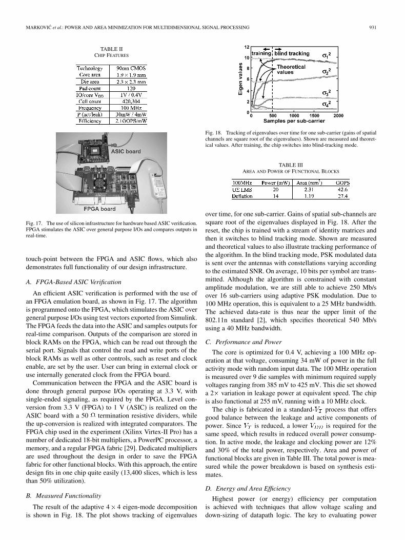
The result of the adaptive 4 4 eigen-mode decompositionis shown in Fig. 18. The plot shows tracking of eigenvalues
Fig. 18. Tracking of eigenvalues over time for one sub-carrier (gains of spatialchannels are square root of the eigenvalues). Shown are measured and theoret-ical values. After training, the chip switches into blind-tracking mode.
TABLE IIIAREA AND POWER OF FUNCTIONAL BLOCKS
over time, for one sub-carrier. Gains of spatial sub-channels aresquare root of the eigenvalues displayed in Fig. 18. After thereset, the chip is trained with a stream of identity matrices andthen it switches to blind tracking mode. Shown are measuredand theoretical values to also illustrate tracking performance ofthe algorithm. In the blind tracking mode, PSK modulated datais sent over the antennas with constellations varying accordingto the estimated SNR. On average, 10 bits per symbol are trans-mitted. Although the algorithm is constrained with constantamplitude modulation, we are still able to achieve 250 Mb/sover 16 sub-carriers using adaptive PSK modulation. Due to100 MHz operation, this is equivalent to a 25 MHz bandwidth.The achieved data-rate is thus near the upper limit of the802.11n standard [2], which specifies theoretical 540 Mb/susing a 40 MHz bandwidth.
C. Performance and Power
The core is optimized for 0.4 V, achieving a 100 MHz op-eration at that voltage, consuming 34 mW of power in the fullactivity mode with random input data. The 100 MHz operationis measured over 9 die samples with minimum required supplyvoltages ranging from 385 mV to 425 mV. This die set showeda 2 variation in leakage power at equivalent speed. The chipis also functional at 255 mV, running with a 10 MHz clock.
The chip is fabricated in a standard- process that offersgood balance between the leakage and active components ofpower. Since is reduced, a lower is required for thesame speed, which results in reduced overall power consump-tion. In active mode, the leakage and clocking power are 12%and 30% of the total power, respectively. Area and power offunctional blocks are given in Table III. The total power is mea-sured while the power breakdown is based on synthesis esti-mates.
D. Energy and Area Efficiency
Highest power (or energy) efficiency per computationis achieved with techniques that allow voltage scaling anddown-sizing of datapath logic. The key to evaluating power

932 IEEE JOURNAL OF SOLID-STATE CIRCUITS, VOL. 42, NO. 4, APRIL 2007
TABLE IVSUMMARY OF 4� 4 MIMO DECODER ASICS
optimality in general is the efficiency metric [30], [31] givenby (3).
(3)
where represents some average operation, such as add ormultiply. Power/energy efficiency is therefore the amount of en-ergy required for some average operation. This means that theefficiency can be improved by scaling down the supply voltageand gate size of the underlying circuits, but this has to be donesimultaneously with architectural selection to maintain the per-formance, and also minimize area/cost of the implementation.
In this study, 12-bit equivalent addition is used as the atomicoperation. Block characterization shows that an equivalent mul-tiply is about 6 times more complex than 12-bit add in termsof area and power. The total computational complexity of thealgorithm implemented is equivalent to 700 12-bit add equiva-lent operations. At 100 MHz, this amounts to 70 GOPS. With34 mW of power, the resulting energy/power efficiency is thus2.1 GOPS/mW.
Presenting the energy efficiency alone could be misleading,since it can be improved by parallelism which increases area.More complete information about the cost of a design is ob-tained by looking into the efficiency of silicon area utilization. Inthis paper, area efficiency is defined as the amount of silicon arearequired to perform an operation per unit time. For highest areaefficiency, the goal is to maximize the utilization of datapathlogic. Interleaving and folding streams of data allows datapathsharing, resulting in the overall chip core area of just 3.5 mm .The area of pipeline registers is about 40% of the total chip area.With 70 GOPS of computational throughput, the chip achieves20 GOPS/mm area efficiency (13.7 GOPS/mm including I/Opads).
A comparison of the the key features of implementationpresented in this paper with other published 4 4 MIMOchips includes modulation, spectral efficiencies, throughputand power, and is summarized in Table IV. For most of thesedesigns, detailed power consumption analysis has not beendisclosed; therefore to asses our design methodology, we
Fig. 19. Area efficiency versus energy efficiency normalized to a 1 V 90 nmprocess. Representative baseband and media ISSCC chips are compared againstthis work.
compare the energy and area efficiency of the SVD chips topublished baseband and media processors [32]–[39]. To makethe comparison fair, the data rate and power are normalized toa 1 V 90 nm technology, and 12-bit wordlengths.
For example, hearing aid DSP processor [39] dissipates660 W of power with a 2.56 MHz clock at 1.05 V, executes50 Million 22-bit operations, with the resulting energy effi-ciency of 75 MOPS/mW in a 0.25 m technology. When scaledto 90 nm and accounting only for switching energy its efficiencyis 2.4 GOPS/mW. If a 12% leakage overhead were included, theresulting efficiency would be 2.1 GOPS/mW, which matchesour result. This stems from the fact that a voltage-scaled 1.05 Vdesign in 0.25 m is equivalent to a 0.42 V in a 1 V 90 nmCMOS. Comparison results are illustrated in Fig. 19. Forexample, the chip presented in [39] achieves similar energyefficiency, but has substantially lower area efficiency, while thechip in [36] reaches similar area efficiency but has lower energyefficiency.
VII. CONCLUSION
This work demonstrates hierarchical energy- and area-ef-ficient mapping of an algorithm into an integrated circuit.Simulink provides the level of abstraction needed for archi-tectural optimizations. The architectural selection is basedon energy-delay-area characterization of datapath logic that

MARKOVIC et al.: POWER AND AREA MINIMIZATION FOR MULTIDIMENSIONAL SIGNAL PROCESSING 933
Fig. 20. Tradeoff between energy efficiency and logic area. Final architecture isoptimized for 0.4 V, which has good static gain for an inverter (shown for processcorners). Other architectural realizations are possible with more parallelism ortime-multiplexing.
allows for comparison of multiple architectural realizations.The choice of architecture is thus highly influenced by powerand performance of the underlying technology. To demonstratethe methodology, a baseband MIMO SVD signal processingalgorithm over multiple carriers has been implemented ina 90 nm CMOS technology, achieving 2.1 GOPS/mW and20 GOPS/mm (13.7 GOPS/mm including I/O pads).
By changing the area or performance constraints, or theoptimization goal, other energy and area efficient architecturescan be derived. For example, these can be obtained by varyingthe level of time-multiplexing or parallelism. Fig. 20 plots thetrade-off between energy efficiency and gate area in variousarchitectures. The dot indicates the design optimized for a0.4 V operation. Starting from this point, energy efficiency canbe traded for smaller area by increasing the level of time-mul-tiplexing, which comes with an increase in supply voltage and,hence, reduced energy efficiency. Going in the direction ofincreased parallelism, the energy efficiency can be improved byfurther scaling down the supply voltage. This result is largelytheoretical, since technology variability limits the minimumpractical supply voltage.
ACKNOWLEDGMENT
The authors thank V. Stojanovic and M. Horowitz for initialwork in sensitivity-based optimization, A. Poon for discussionsabout the SVD algorithm, C. Shi for maintaining the FFC tool,B. Richards for automating the ASIC tool flow, and P. Droz,C. Chang, and H. Chen for help with chip testing infrastructure.The authors acknowledge Xilinx for FPGA hardware support.
REFERENCES
[1] J. Thomson et al., “An integrated 802.11a baseband and MAC pro-cessor,” in IEEE Int. Solid-State Circuits Conf. Dig. Tech. Papers, Feb.2002, pp. 126–127.
[2] IEEE 802.11 Wireless Local Area Networks—The Working Group forWLAN Standards. [Online]. Available: http://grouper.ieee.org/groups/802/11/
[3] D. Tse and P. Viswanath, Fundamentals of Wireless Communication.Cambridge, U.K.: Cambridge Univ. Press, 2005.
[4] G. Foschini, “Layered space-time architecture for wireless communi-cation in a fading environment when using multi-element antennas,”Bell Labs Tech. J., pp. 41–59, 1996.
[5] G. Foschini, G. Golden, R. Valenzuela, and P. Wolniansky, “Simpli-fied processing for high spectral efficiency wireless communicationemploying multi-element arrays,” IEEE J. Sel. Areas Commun., vol.17, no. 11, pp. 1841–1852, Nov. 1999.
[6] D. Rabideau, “Fast, rank adaptive subspace tracking and applications,”IEEE Trans. Signal Process., vol. 44, no. 9, pp. 2229–2244, Sep. 1996.
[7] J. Laurila, K. Kopsa, R. Schurhuber, and E. Bonek, “Semi-blind sep-aration and detection of co-channel signals,” in Proc. Int. Conf. Com-munications, Jun. 1999, vol. 1, pp. 17–22.
[8] A. Poon, D. Tse, and R. W. Brodersen, “An adaptive multiple-antennatransceiver for slowly flat-fading channels,” IEEE Trans. Commun.,vol. 51, no. 11, pp. 1820–1827, Nov. 2003.
[9] C. V. Ramamoorthy, J. R. Goodman, and K. H. Kim, “Some propertiesof iterative square-rooting methods using high-speed multiplication,”IEEE Trans. Comput., vol. C-21, no. 8, pp. 837–847, 1972.
[10] D. Markovic, B. Nikolic, and R. W. Brodersen, “Power and area ef-ficient VLSI architectures for communication signal processing,” inProc. Int. Conf. Communications, Jun. 2006.
[11] D. Markovic, V. Stojanovic, B. Nikolic, M. A. Horowitz, and R. W.Brodersen, “Methods for true energy-performance optimization,” IEEEJ. Solid-State Circuits, vol. 39, pp. 1282–1293, Aug. 2004.
[12] V. Zyuban et al., “Integrated analysis of power and performance forpipelined microprocessors,” IEEE Trans. Comput., vol. 53, no. 8, pp.1004–1016, Aug. 2004.
[13] V. Srinivasan et al., “Optimizing pipelines for power and perfor-mance,” in Proc. IEEE/ACM Int. Symp. Microarchitecture, Nov. 2002,pp. 333–344.
[14] SystemC. [Online]. Available: http://systemc.org[15] W. R. Davis et al., “A design environment for high throughput, low
power dedicated signal processing systems,” IEEE J. Solid-State Cir-cuits, vol. 37, no. 3, pp. 420–431, Mar. 2002.
[16] C. Chang, K. Kuusilinna, B. Richards, A. Chen, N. Chan, and R. W.Brodersen, “Rapid design and analysis of communication systemsusing the BEE hardware emulation environment,” in Proc. IEEE RapidSystem Prototyping Workshop, Jun. 2003.
[17] T. Gemmeke, M. Gansen, H. J. Stockmanns, and T. G. Noll,“Design optimization of low-power high-performance DSP buildingblocks,” IEEE J. Solid-State Circuits, vol. 39, no. 7, pp. 1131–1139,Jul. 2004.
[18] C. Shi and R. W. Brodersen, “Automated fixed-point data-type opti-mization tool for signal processing and communication systems,” inProc. IEEE Design Automation Conf., Jun. 2004, pp. 478–483.
[19] C. Shi and R. W. Brodersen, “A perturbation theory on statisticalquantization effects in fixed-point DSP with non-stationary inputs,”in Proc. Int. Symp. Circuits and Systems (ISCAS 2004), May2004, pp. 373–376.
[20] C. Shi, “Floating-point to fixed-point conversion,” Ph.D. dissertation,Univ. California, Berkeley, 2004.
[21] A. P. Chandrakasan, S. Sheng, and R. W. Brodersen, “Low-powerCMOS digital design,” IEEE J. Solid-State Circuits, vol. 27, no. 4, pp.473–484, Apr. 1992.
[22] J. Rabaey, A. Chandrakasan, and B. Nikolic, Digital Integrated Cir-cuits: A Design Perspective, 2nd ed. Upper Saddle River, NJ: Pren-tice-Hall, 2003.
[23] K. K. Parhi, VLSI Digital Signal Processing Systems. New York:Wiley, 1999.
[24] V. Srinivasan and R. Vemuri, “A retiming based relaxation heuristicfor resource-constrained loop pipelining,” in Proc. 11th Int. Conf. VLSIDesign: VLSI for Signal Processing, Jan. 1998, vol. 2, pp. 435–441.
[25] Y. Yi, R. Woods, L. K. Ting, and C. F. N. Cowna, “High samplingrate retimed DLMS filter implementation in Virtex-II FPGA,” in IEEEWorkshop on Signal Processing Systems, Oct. 2002, pp. 139–145.
[26] D. Markovic, “A power/area optimal approach to VLSI signal pro-cessing,” Ph.D. dissertation, Univ. California, Berkeley, 2006.
[27] D. Markovic, R. W. Brodersen, and B. Nikolic, “A 70 GOPS, 34 mWmulti-carrier MIMO chip in 3.5 mm ,” in Proc. Int. Symp. VLSI Cir-cuits, Jun. 2006, pp. 196–197.
[28] K. Usami et al., “Automated low-power technique exploiting multiplesupply voltages applied to a media processor,” IEEE J. Solid-State Cir-cuits, vol. 33, no. 3, pp. 463–472, Mar. 1998.
[29] BEE2: Berkeley Emulation Engine 2. [Online]. Available: http://bwrc.eecs.berkeley.edu/Research/BEE/BEE2/index.htm

934 IEEE JOURNAL OF SOLID-STATE CIRCUITS, VOL. 42, NO. 4, APRIL 2007
[30] R. Brodersen, “Technology, architecture, and applications,” presentedat the IEEE Int. Solid-State Circuits Conf. Dig. Tech. Papers, SpecialTopic Evening Session: Low Voltage Design for Portable Systems, Feb.2002.
[31] T. A. C. M. Claasen, “High speed: Not the only way to exploit theintrinsic computational power of silicon,” in IEEE Int. Solid-State Cir-cuits Conf. Dig. Tech. Papers, Feb. 1999, pp. 22–25.
[32] S. Santhanam et al., “A low-cost 300 MHz RISC CPU with attachedmedia processor,” in IEEE Int. Solid-State Circuits Conf. Dig. Tech.Papers, Feb. 1998, pp. 298–299.
[33] J. Williams et al., “A 3.2 GOPS multiprocessor DSP for communica-tion applications,” in IEEE Int. Solid-State Circuits Conf. Dig. Tech.Papers, Feb. 2000, pp. 70–71.
[34] T. Ikenaga and T. Ogura, “A fully-parallel 1Mb CAM LSI for real-time pixel-parallel image processing,” in IEEE Int. Solid-State CircuitsConf. Dig. Tech. Papers, Feb. 1999, pp. 264–265.
[35] M. Wosnitza, M. Cavadini, M. Thaler, and G. Troster, “A high pre-cision 1024-point FFT processor for 2-D convolution,” in IEEE Int.Solid-State Circuits Conf. Dig. Tech. Papers, Feb. 1998, pp. 118–119.
[36] F. Arakawa et al., “An embedded processor core for consumer ap-pliances with 2.8 GFLOPS and 36 M polygons/s FPU,” in IEEE Int.Solid-State Circuits Conf. Dig. Tech. Papers, Feb. 2004, pp. 334–335.
[37] M. Strik et al., “Heterogeneous multi-processor for the management ofreal-time video and graphics streams,” in IEEE Int. Solid-State CircuitsConf. Dig. Tech. Papers, Feb. 2000, pp. 244–245.
[38] H. Igura et al., “An 800 MOPS 110 mW 1.5 V parallel DSP for mobilemultimedia processing,” in IEEE Int. Solid-State Circuits Conf. Dig.Tech. Papers, Feb. 1998, pp. 292–293.
[39] P. Mosch et al., “A 720 �W 50 MOPs 1 V DSP for a hearing aid chipset,” in IEEE Int. Solid-State Circuits Conf. Dig. Tech. Papers, Feb.2000, pp. 238–239.
[40] A. Burg et al., “VLSI implementation of MIMO detection using thesphere decoding algorithm,” IEEE J. Solid-State Circuits, vol. 40, no.7, pp. 1566–1577, Jul. 2005.
[41] D. Garrett, G. Woodward, L. Davis, G. Knagge, and C. Nicol, “A 28.8Mb/s 4� 4 MIMO 3G high speed downlink packet access receiver withnormalized least mean square equalization,” in IEEE Int. Solid-StateCircuits Conf. Dig. Tech. Papers, Feb. 2004, pp. 420–421.
[42] D. Garrett, G. Woodward, L. Davis, and C. Nicol, “A 28.8 Mb/s 4� 4MIMO 3G CDMA receiver for frequency selective channels,” IEEE J.Solid-State Circuits, vol. 40, no. 1, pp. 320–330, Jan. 2005.
[43] Z. Guo and P. Nilsson, “A VLSI architecture for the schnorr-euchnerdecoder for MIMO systems,” in Proc. IEEE CAS Symp. EngineeringTechnologies: Frontiers of Mobile and Wireless Communications, Jun.2004, pp. 65–68.
[44] Z. Guo, “MIMO decoding, algorithm and implementation,” Ph.D. dis-sertation, Lund Univ., Lund, Sweden, 2005.
[45] Z. Guo and P. Nilsson, “A VLSI implementation of MIMO detectionfor future wireless communications,” in Proc. IEEE Symp. Personal,Indoor, and Mobile Radio Commun., Sep. 2003, pp. 2852–2856.
Dejan Markovic (S’96–M’06) received the Dipl.Ing.degree from the University of Belgrade, Yugoslavia,in 1998, and the M.S. and Ph.D. degrees from theUniversity of California, Berkeley, in 2000 and 2006,respectively, all in electrical engineering.
In 2006, he joined the faculty of the Electrical En-gineering Department at the University of California,Los Angeles, as an Assistant Professor. His researchis focused on rapid prototyping and optimization ofpower limited digital systems, with emphasis on thenext generation wireless communication devices.
Dr. Markovic was awarded the CalVIEW Fellow Award in 2001 and 2002for excellence in teaching and mentoring of industry engineers through the UCBerkeley distance learning program. In 2004, he was a co-recipient of the BestPaper Award at the IEEE International Symposium on Quality Electronic De-sign.
Borivoje Nikolic (S’93–M’99–SM’06) received theDipl.Ing. and M.Sc. degrees in electrical engineeringfrom the University of Belgrade, Yugoslavia, in 1992and 1994, respectively, and the Ph.D. degree from theUniversity of California at Davis in 1999.
He was on the faculty of the University ofBelgrade from 1992 to 1996. He spent two yearswith Silicon Systems, Inc., Texas InstrumentsStorage Products Group, San Jose, CA, working ondisk-drive signal processing electronics. In 1999, hejoined the Department of Electrical Engineering and
Computer Sciences, University of California at Berkeley, where he is now anAssociate Professor. His research activities include high-speed and low-powerdigital integrated circuits and VLSI implementation of communications andsignal processing algorithms. He is coauthor of the book Digital IntegratedCircuits: A Design Perspective, 2nd ed. (Prentice-Hall, 2003).
Dr. Nikolic received the IBM Faculty Partnership Award in 2005, NSF CA-REER award in 2003, College of Engineering Best Doctoral Dissertation Prizeand Anil K. Jain Prize for the Best Doctoral Dissertation in Electrical and Com-puter Engineering at University of California at Davis in 1999, as well as theCity of Belgrade Award for the Best Diploma Thesis in 1992. For work withhis students and colleagues he received the Best Paper Award at the ACM/IEEEInternational Symposium of Low-Power Electronics in 2005, and the 2004 JackKilby Award for the Outstanding Student Paper at the IEEE International Solid-State Circuits Conference.
Robert W. Brodersen (M’76–SM’81–F’82) re-ceived the Ph.D. degree from the MassachusettsInstitute of Technology, Cambridge, in 1972.
He was then with the Central Research Laboratoryat Texas Instruments for three years. Following that,he joined the Electrical Engineering and ComputerScience faculty of the University of California atBerkeley, where he is now the John Whinnery ChairProfessor and Co-Scientific Director of the BerkeleyWireless Research Center. His research is focusedin the areas of low-power design and wireless
communications and the CAD tools necessary to support these activities.Prof. Brodersen has won best paper awards for a number of journal and con-
ference papers in the areas of integrated circuit design, CAD and communica-tions, including in 1979 the W.G. Baker Award. In 1983, he was co-recipient ofthe IEEE Morris Liebmann Award. In 1986, he received the Technical Achieve-ment Awards in the IEEE Circuits and Systems Society and in 1991 from theSignal Processing Society. In 1988, he was elected to be member of the NationalAcademy of Engineering. In 1996, he received the IEEE Solid-State CircuitsSociety Award and in 1999 received an honorary doctorate from the Universityof Lund in Sweden. In 2000, he received a Millennium Award from the Cir-cuits and Systems Society, the Golden Jubilee Award from the IEEE. In 2001he was awarded the Lewis Winner Award for outstanding paper at the IEEE In-ternational Solid-State Circuits Conference and in 2003 was given an award forbeing one of the top ten contributors over the 50 years of that conference.