a 0.5 v 8‑12 bit 300 ksps sar adc with adaptive conversion
TRANSCRIPT
This document is downloaded from DR‑NTU (https://dr.ntu.edu.sg)Nanyang Technological University, Singapore.
A 0.5 V 8‑12 bit 300 KSPS SAR ADC with adaptiveconversion time detection‑and‑control for highimmunity to PVT variations
Kim, Ju Eon; Yoo, Taegeun; Jung, Dong‑Kyu; Yoon, Dong‑Hyun; Seong, Kiho; Kim, TonyTae‑Hyoung; Baek, Kwang‑Hyun
2020
Kim, J. E., Yoo, T., Jung, D.‑K., Yoon, D.‑H., Seong, K., Kim, T. T.‑K., & Baek, K.‑H. (2020). A 0.5V 8‑12 bit 300 KSPS SAR ADC with adaptive conversion time detection‑and‑control for highimmunity to PVT variations. IEEE Access, 8, 101359‑101368.doi:10.1109/access.2020.2998161
https://hdl.handle.net/10356/145808
https://doi.org/10.1109/ACCESS.2020.2998161
© 2020 IEEE. This journal is 100% open access, which means that all content is freelyavailable without charge to users or their institutions. All articles accepted after 12 June2019 are published under a CC BY 4.0 license, and the author retains copyright. Users areallowed to read, download, copy, distribute, print, search, or link to the full texts of thearticles, or use them for any other lawful purpose, as long as proper attribution is given.
Downloaded on 23 Feb 2022 00:59:14 SGT

Received May 4, 2020, accepted May 25, 2020, date of publication May 28, 2020, date of current version June 10, 2020.
Digital Object Identifier 10.1109/ACCESS.2020.2998161
A 0.5 V 8–12 Bit 300 KSPS SAR ADC With AdaptiveConversion Time Detection-and-Control for HighImmunity to PVT VariationsJU EON KIM 1, (Member, IEEE), TAEGEUN YOO 1, (Member, IEEE),DONG-KYU JUNG 2, (Student Member, IEEE),DONG-HYUN YOON 2, (Student Member, IEEE),KIHO SEONG 2, (Student Member, IEEE), TONY TAE-HYOUNG KIM 1, (Senior Member, IEEE),AND KWANG-HYUN BAEK 2, (Senior Member, IEEE)1School of Electrical and Electronic Engineering, Nanyang Technological University, Singapore 6397982School of Electrical and Electronics Engineering, Chung-Ang University, Seoul 06974, South Korea
Corresponding author: Kwang-Hyun Baek ([email protected])
This work was supported in part by the Technology Innovation Program (or the Industrial Strategic Technology Development Program)and Royalty Free Processor and Software Platform Development for Low Power IoT and Wearable Device Devices funded by the Ministryof Trade, Industry and Energy (MOTIE, South Korea) under Grant 10077381, and in part by the National Research Foundation ofKorea (NRF) Grant funded by the Korea Government (MSIT) under Grant 2020R1A2C1012714.
ABSTRACT In this paper, a low power asynchronous successive approximation register (SAR) analog-to-digital converter (ADC) involving the process, voltage, and temperature (PVT) compensation is presented.A proposed adaptive conversion time detection-and-control technique enhances the power efficiency,covering wide PVT variations. The proposed detection-and-control technique senses PVT variation in anaspect of conversion time, and adaptively controls the operation speed and power consumption. For PVTcompensation, the proposed architecture includes the local supply/ground voltage. The local supply/groundvoltage makes high |VGS| for transistors in the comparator and capacitive digital-to-analog converterswitches, resulting in enhanced operation speed. However, when PVT condition changes to be favorablefor the conversion speed, the |VGS| decreases for low power consumption. 30 chips were measured to verifythe proposed ADC. Having the proposed architecture tested with 10 kHz input frequency, SNDR remainedhigher than 60 dB at unfavorable conditions such as −9 % supply voltage variation, or −20 ◦C temperaturevariation. On the other hand, at favorable conditions such as +9 % supply voltage variation, or 80 ◦Ctemperature variation, the power consumption of SAR ADC decreased without performance degradation.
INDEX TERMS Asynchronous, compensation, low power, process voltage temperature (PVT), successiveapproximation register (SAR) analog-to-digital converter (ADC).
I. INTRODUCTIONThe successive approximation register (SAR) analog-to-digital converters (ADCs) are the most promising candi-date for low power applications such as battery-poweredsensor nodes and bio-medical systems. SAR ADCs operat-ing at low supply voltage for power efficiency have beenreported [1]–[9]. Since using the low supply voltage cancause problems such as leakage current or low signal-to-noise
The associate editor coordinating the review of this manuscript and
approving it for publication was Omid Kavehei .
ratio (SNR), many studies mainly have focused on the leak-age current or low SNR. However, the low supply voltageSAR ADCs are also vulnerable to process, voltage, and tem-perature (PVT) variations. Recently, several ADCs involvedtemperature compensation technique for comparator underthe low supply voltage, and PVT-stabilized technique fordynamic amplifiers [9]–[11]. Besides these problems, conver-sion speed also can be severely affected by PVT variations.Due to the uncertainty of PVT variations, ADCs should havemuch faster conversion speed than target specifications. How-ever, it causes unnecessary power consumption at the PVT
VOLUME 8, 2020 This work is licensed under a Creative Commons Attribution 4.0 License. For more information, see https://creativecommons.org/licenses/by/4.0/ 101359

J. E. Kim et al.: 0.5 V 8–12 Bit 300 KSPS SAR ADC With Adaptive Conversion Time Detection-and-Control
conditions that are favorable for the conversion speed. WhenMOSFET is operating in the subthreshold region, the draincurrent is
ID = I0exp(VGS − VTH
mUT)(1− exp
(−VDSUT
)) (1)
where I0 = µ0Cox(W/L)U2T (m− 1), andµ0,Cox ,UT , andm
denote the carriermobility, gate oxide capacitance, thermody-namic voltage (kT/q), and subthreshold slope factor, respec-tively [9], [12]–[13]. The high sensitivity of drain current toPVT variations can be inferred by using (1) [13]. Fig. 1. showsa normalized conversion time at the worst-case corner andtemperature conditions depending on the supply voltage. Thenormalized conversion time means that the longest conver-sion times are divided by the conversion time that is requiredat the TT, 27 ◦C. When the supply voltage is 1.2 V, the con-version time becomes longer by 1.28-times at the SS and80 ◦C in comparison with the conversion time at the TT and27 ◦C. For 0.5 V supply voltage, the conversion time becomeslonger by 7.66-times at the SS and −20 ◦C in comparisonwith the conversion time at the TT and 27 ◦C. These variationsresult in accuracy degradation due to incomplete conversionin asynchronous SARADC. In other words, the ADCs having1.2 V supply voltage should have 1.28-times faster conver-sion speed than the speed that is required at the TT and 27 ◦C,which prevents performance degradation at the SS and 80 ◦C.However, for the ADCs having 0.5 V supply voltage, theconversion speed should be 7.66-times faster, which impliesmuch larger power consumption. Therefore, in this paper, alow-power SAR ADC with full consideration of PVT vari-ations is proposed. The proposed system detects the PVTvariation by monitoring the conversion speed and then con-trols the supply voltage to reduce power consumption. Fig. 2.shows the PVT compensation and reduction in current bycontrolling the supply voltage depending on PVT condition.As shown in Fig. 2., the conversion time becomes short byincreasing the supply voltage to compensate for the PVTvariations. In the case of the other PVT conditions, the supplyvoltage level becomes lower for low power operation, whichdoes not cause performance degradation. Section II will dis-cuss the proposed architecture for sensing and compensatingthe PVT variation. In sections III and IV, the implementationof the proposed SAR ADC and measurement results will bepresented. Lastly, a conclusion will be drawn in sections V.
II. PVT COMPENSATION SYSTEMFig. 3. shows the conceptual block diagram of the proposedPVT compensation system. The supply voltage generatorsupports the ADC’s global supply voltage, and the IADCrepresents the current. Once the ‘PVT SENSING’ block givesthe information of PVT to the ‘Local supply/ground’ blocks,local supply/ground voltages of ‘comparator’ and ‘switches’of a capacitive digital-to-analog converter (C-DAC) areadjusted. In the SAR ADC operation, the comparison timeof the comparator, and settling time of C-DAC have alarge portion of the overall conversion speed. This problem
FIGURE 1. Normalized conversion time at the worst-case corner andtemperature conditions with various supply voltages from 0.5 V to 1.2 V.
FIGURE 2. (a) The process, voltage, and temperature (PVT) conditions thatrequire acceleration by increasing VDD (supply voltage) and (b) the otherPVT conditions that can reduce the current for low power operation.
becomes worse when the resolution of ADC increases. Thus,the change in local supply/ground voltages for these blockscan control the conversion speed of ADC, as describedin Fig. 2. (a). If PVT changes to be favorable for the con-version speed, local supply/ground voltages become originalvalues like Fig. 2. (b) to reduce the IADC of Fig. 3, whichassuring low power consumption.
A. SENSING THE PVT VARIATIONSPVT SENSING block senses conversion speed (or conver-sion time) to sense the PVT variations. Since SAR ADCdetermines each bit in consecutive order, the least-significant-bit (LSB) decision denotes the end-of-conversion (EOC).
101360 VOLUME 8, 2020

J. E. Kim et al.: 0.5 V 8–12 Bit 300 KSPS SAR ADC With Adaptive Conversion Time Detection-and-Control
FIGURE 3. The conceptual block diagram of the proposed PVTcompensation system.
The detection logic compares the EOCwith the next samplingclock that is synchronized by the reference clock to monitorthe conversion speed [14]. If conversion speed becomes tooslow to complete the conversion, the next sampling clockprecedes the EOC. In this case, the PVT SENSING blockincreases the thermometer code (DDNC) to accelerate theconversion speed. However, at some PVT conditions such asFF corner, higher supply voltage, or 80 ◦C, the acceleratedconversion speed causes large power consumption. There-fore, if the EOC precedes the next sampling clock becauseof fast conversion speed, the PVT SENSING block decreasesthe DDNC to decelerate the conversion speed and reduce thepower consumption. After several sequences of the trackingPVT,DDNC has two repeated codes in the locking state. Fig. 4.shows a locking state and the criteria to prevent the LSB-missing in the locking state. Since the deceleration of conver-sion speed can cause LSB-missing, the PVT SENSING blockcompares the sampling clock with a delayed EOC (DEOC)that is the delayed signal from EOC by Tdelay. Moreover,if the conversion time variation by changing DDNC (1Tcom)is too large, LSB-missing occurs in the locking state. There-fore,1Tcom should be shorter than Tdelay, i.e., detection-and-control has the following criteria.
Tdelay > |1Tcom| (2)
B. COMPENSATING PVT VARIATIONSLocal supply/ground voltage can be easily realized by capac-itor switching by using a temporal voltage shift because allsub-blocks of SAR ADC are the dynamic circuits. The localsupply/ground voltage increases before the operation, and thesub-blocks operate fast with a high |VGS| and |VDS|. Forconvenience, only |VGS| will be mentioned in this paper.After the operation of sub-blocks, the capacitors are chargedagain during the reset phase. The local supply/ground voltagehas a multi-level, and the DDNC determines the voltage level.The number of levels determines the resolution of the con-trol of power consumption. However, increasing the numberof levels leads to the burdens of hardware complexity and
power consumption, which cancels out the benefits. More-over, the maximum number of cycles to find the locking statealso increases.
III. IMPLEMENTATIONFig. 5. shows a block diagram of the proposed SAR ADC.It consists of 8-12-bit reconfigurable split-capacitor C-DAC,detection-N-control (DNC), adaptively accelerating C-DACsettling switch (ACS), and adaptively boosting comparator(ABC) blocks. The following sections show each block indetail.
A. DETECTION-N-CONTROL (DNC)As shown in Fig. 5., the DNC consists of dividers, a phasedetector (PD), a delay block, and a thermometer counter.The PD determines whether the SAR operation is fast ornot by comparing the DEOC with the next sampling clock.If DEOC rises before the next sampling clock, UP/DOWNbecomes LOW. On the contrary, UP/DOWN becomes HIGHif DEOC does not precede the next sampling clock. Depend-ing on the UP/DOWN signal, 4-bit (5 levels) thermometercode (DDNC <3:0>) increases or decreases, and ACS andABC block uses the value to control the local supply/groundvoltage. In this design, after the ADCwakes up, themaximumnumber of cycles is 4. In the case of increasing DDNC <3:0>,the duration for comparison and C-DAC settling gets shorter.The delay block makes the delay time from EOC to DEOC(Tdelay) where the time duration of the delay cell is deter-mined by (2). Delay block consists of inverters, and thenumber of inverters is determined by the worst-case PVTconditions to guarantee the condition of (2). Two T-F/F makethe 1/2 divided and 1/4 divided CK_SAM clock (period ofeach signal is 2× and 4× period of CK_SAM) for PVTdetection, and DDNC update, respectively. In other words, thecompensation procedure is repeated every four conversioncycles and fully utilizes the given conversion time for low-power operations.
B. VDD-BOOSTER AND VSS-SINKER FOR MULTI-LEVELSUPPLY/GROUND VOLTAGETheVDD-Booster andVSS-Sinker blocks generate themulti-level supply/ground voltage adaptively to compensate for thePVT variation. Fig. 6. shows the schematics of VDD-Boosterand VSS-Sinker. The VDD-Booster generates a higher volt-age than the supply voltage by switching the capacitors. Theincreased voltages of the VDDBoost node are proportional tothe number of switched capacitors among the capacitor bank.DACL is a synchronized DDNC by CK signal for capacitorswitching. In the case of VDD-Booster, when CK is HIGH,the capacitors are charged, and the voltage of VDDBoostbecomes VDD. At the falling edge of CK, the gate of MPbecomes HIGH, so that MP turns off. Then, the bottom ofthe capacitor switches from the ground to VDD. To preventthe leakage current by high VDDBoost voltage, the gate andbody nodes of MP rise to VDDBoost voltage. Even if the gateand body nodes of MP do not rise to the VDDBoost voltage,
VOLUME 8, 2020 101361

J. E. Kim et al.: 0.5 V 8–12 Bit 300 KSPS SAR ADC With Adaptive Conversion Time Detection-and-Control
FIGURE 4. A locking state and criteria to prevent the least-significant-bit (LSB) missing.
FIGURE 5. Block diagram of proposed ADC.
the momentary leakage current can be ignored. When CKbecomes HIGH again, the gate of MP becomes LOW, andthe bottom of capacitors switches from VDD to ground. TheVSS-Sinker block operates similarly as the VDD-Boosterblock.
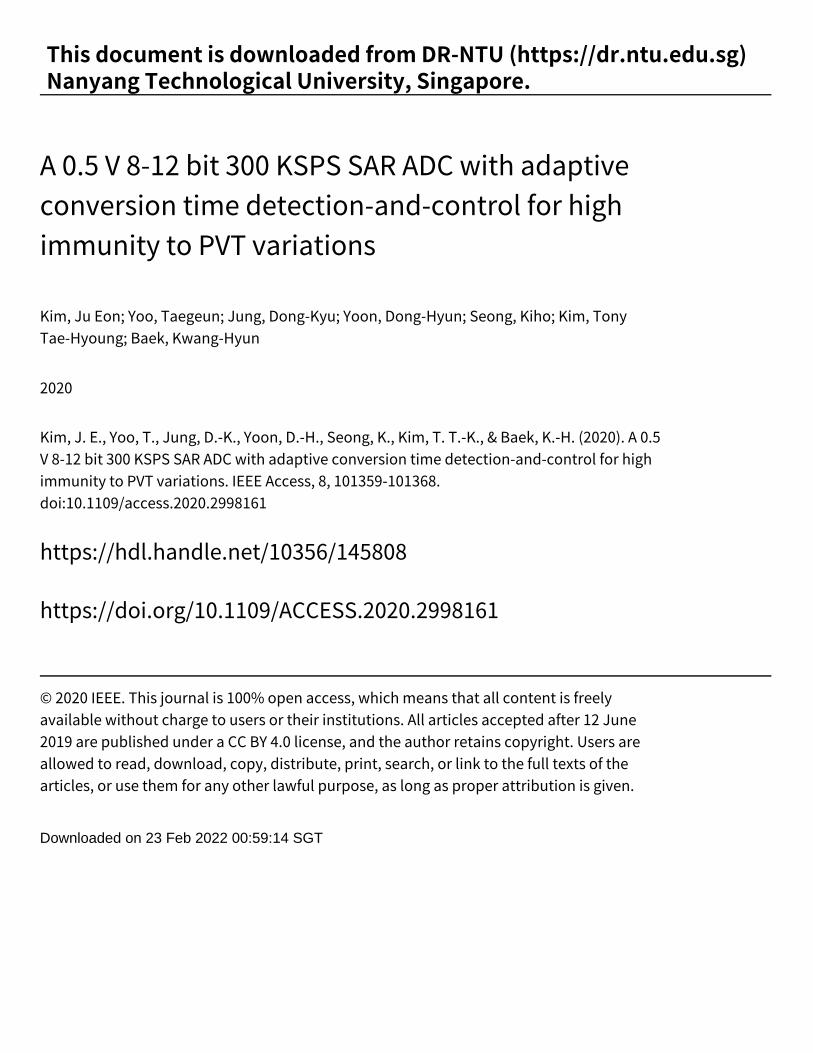
C. ADAPTIVE ACCELERATION C-DAC SETTLINGSWITCH (ACS)Since the capacitance of C-DAC exponentially increaseswith a resolution of ADC, C-DAC settling time shoulddecrease to speed up the SAR operation. Fig. 7. (a) shows
the implementation for adaptively accelerating the C-DACsettling switch (ACS). To enhance the C-DAC settling speed,VDD-Booster and VSS-Sinker are used to S-inverters (smallW/L) driving L-inverters (large W/L) which drive the capac-itors of C-DAC. In the split capacitor C-DAC [15], COMPX(COMPP or COMPN) nodes and MX (M1 or M2) nodeschange fromHIGH to LOW and from LOW to HIGH, respec-tively, during C-DAC switching. In a differential split capac-itor C-DAC, four capacitors (Cn) take a role in one bit, andthus, four S-inverters share a single VDD-Booster and VSS-Sinker. The |VGS|s of PMOS and NMOS in the S-inverter are
101362 VOLUME 8, 2020

J. E. Kim et al.: 0.5 V 8–12 Bit 300 KSPS SAR ADC With Adaptive Conversion Time Detection-and-Control
FIGURE 6. Schematic of (a) VDD-Booster and (b) VSS-Sinker for localsupply/ground voltages.
increased by VDD-Booster and VSS-Sinker blocks. The tem-poral changes in source voltages provide a higher |VGS| to thesmall inverter and help driving L-inverter with higher current.Then, higher |VGS| provided sequentially to L-inverter resultsin the acceleration for the C-DAC switching. Fig. 7. (b) showsthe effect of C-DAC acceleration. At a start of sampling(rising edge of CK_SAM), VDDBoost and VSSSINK nodeschange in advance. After sampling and prior-switchings,COMPX signal changes from HIGH to LOW. Because ofhigher |VGS|, the switching of the bottom plate (CBOT)becomes faster. The capacitances of switching capacitors inthe VDD-Booster and VSS-Sinker blocks are large enoughregarding leakage current and accelerated speed.
The proposed SAR ADC adopts a multi-period clock gen-erator [14]. Themulti-period clock generator selects the num-ber of buffers according to DDNC, controlling the period ofcomparator clocks suitable for the C-DAC switching speed.
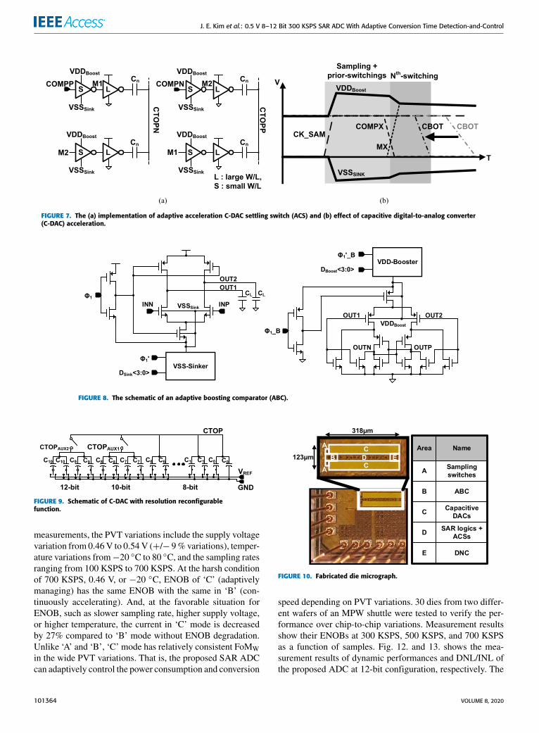
D. ADAPTIVE BOOSTING COMPARATOR (ABC)Fig. 8. shows the schematic of the adaptive boosting com-parator (ABC). The ABC comprises of an integrator-basedamplifier and the latch [16]. VDD-Booster and VSS-Sinkerare used to the second stage and the first stage, respectively.At a reset phase, the voltages of OUT1/OUT2 are VDD, andoutputs of the second stage are LOW. During an evaluationphase, the OUT1/OUT2 nodes decrease with different speedsaccording to the input differences. The second stage uses thedifference between OUT1/OUT2 nodes to determine the out-put of the comparator (OUTN/OUTP). Without acceleration,the discharging for load capacitors of the first stage takesa longer time, and the metastability problem of the secondstage can be even worse. With acceleration, DSink and DBoostsignals that are decoded from DDNC and synchronized withclock(8) switch the bottom of capacitors of VSS-Sinkerand VDD-Booster. Switching capacitors in VSS-Sinker andVDD-Booster blocks increase the |VGS| of input transistors ineach stage. Consequentially, the ABC archives fast discharg-ing and the decision. Table. 1. shows the simulation results
TABLE 1. Simulation results and noise budget.
TABLE 2. Summary of dynamic performance at 8 and 10-bit modes.
of the noise and comparison time (Tcomp) of the ABC. Thenoise includes quantization noise (VQ), thermal noise (VT),and comparator noise (VC). The simulation results show thatthe comparison time at SS corner and −20 ◦C is longer thanthat of TT and 27 ◦C without boosting. However, with theboosting, the comparison time decreases without degradationof SNR compared with TT, 27 ◦C.
E. RECONFIGURABLE C-DACThe proposed SAR ADC also has the resolution reconfig-urable functions [17]. Fig. 9. shows the schematic of theC-DAC with the resolution reconfigurability. External digitalcodes for the reconfigurable operation connect additionalcapacitors to 8-bit C-DAC. The switches between CTOP nodeand CTOPAUX1 or CTOPAUX2 are 2.5V NMOS transistors(I/O transistor), and the gate voltage swing is 2.5V for thelinearity.
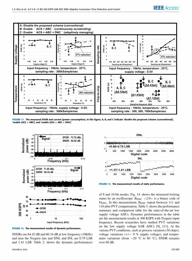
IV. MEASUREMENTSThe prototype was fabricated in 65 nm CMOS, and the sizeis 0.039 mm2 (0.318 mm × 0.123 mm). Fig. 10. showsthe fabricated die micrograph. Even though ADC involvesthe VDD-Booster, VSS-Sinker, and DNC blocks, there isno extra area for them because the C-DAC area dominatesthe ADC area. The temperature chamber changed the chiptemperature, and the power supply changed the supply volt-age. Lastly, 30 chips from 2 wafers were measured to con-sider process variation. Fig. 11. shows the measured ENOBand current where A, B, and C indicate ‘disable the pro-posed scheme (conventional),’ ‘enable (ACS + ABC),’ and‘enable (ACS + ABC + DNC),’ respectively. In these
VOLUME 8, 2020 101363
J. E. Kim et al.: 0.5 V 8–12 Bit 300 KSPS SAR ADC With Adaptive Conversion Time Detection-and-Control
FIGURE 7. The (a) implementation of adaptive acceleration C-DAC settling switch (ACS) and (b) effect of capacitive digital-to-analog converter(C-DAC) acceleration.
FIGURE 8. The schematic of an adaptive boosting comparator (ABC).
FIGURE 9. Schematic of C-DAC with resolution reconfigurablefunction.
measurements, the PVT variations include the supply voltagevariation from 0.46V to 0.54V (+/− 9%variations), temper-ature variations from−20 ◦C to 80 ◦C, and the sampling ratesranging from 100 KSPS to 700 KSPS. At the harsh conditionof 700 KSPS, 0.46 V, or −20 ◦C, ENOB of ‘C’ (adaptivelymanaging) has the same ENOB with the same in ‘B’ (con-tinuously accelerating). And, at the favorable situation forENOB, such as slower sampling rate, higher supply voltage,or higher temperature, the current in ‘C’ mode is decreasedby 27% compared to ‘B’ mode without ENOB degradation.Unlike ‘A’ and ‘B’, ‘C’ mode has relatively consistent FoMWin the wide PVT variations. That is, the proposed SAR ADCcan adaptively control the power consumption and conversion
FIGURE 10. Fabricated die micrograph.
speed depending on PVT variations. 30 dies from two differ-ent wafers of an MPW shuttle were tested to verify the per-formance over chip-to-chip variations. Measurement resultsshow their ENOBs at 300 KSPS, 500 KSPS, and 700 KSPSas a function of samples. Fig. 12. and 13. shows the mea-surement results of dynamic performances and DNL/INL ofthe proposed ADC at 12-bit configuration, respectively. The
101364 VOLUME 8, 2020
J. E. Kim et al.: 0.5 V 8–12 Bit 300 KSPS SAR ADC With Adaptive Conversion Time Detection-and-Control
FIGURE 11. The measured ENOB and current (power consumption). In this figure, A, B, and C indicate ‘disable the proposed scheme (conventional)’,‘enable (ACS + ABC)’, and ‘enable (ACS + ABC + DNC)’.
FIGURE 12. The measurement results of dynamic performance.
SNDRs are 64.42 dB and 60.34 dB at low frequency (10kHz)and near the Nyquist rate and DNL and INL are 0.79 LSBand 1.41 LSB. Table 2. shows the dynamic performances
FIGURE 13. The measurement results of static performance.
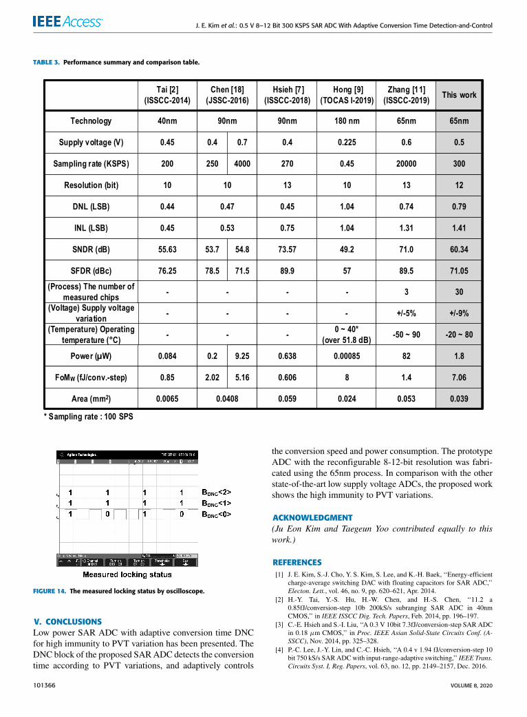
of 8 and 10-bit modes. Fig. 14. shows the measured lockingstatus by an oscilloscope. BDNC <2:0> is a binary code ofDDNC. In this measurement, BDNC repeat between 111 and110 after PVT compensation. Table 3. shows the performancesummary and comparison table for the state-of-the-art lowsupply voltage ADCs. Dynamic performances in the tableare the measurement results at 300 KSPS with Nyquist inputfrequency. Recent researches have studied PVT variationson the low supply voltage SAR ADCs [9], [11]. At thevarious PVT conditions, such as process variation (30 chips),voltage variations (+/− 9 % supply voltage), and temper-ature variations (from −20 ◦C to 80 ◦C), SNDR remainsover 60 dB.
VOLUME 8, 2020 101365
J. E. Kim et al.: 0.5 V 8–12 Bit 300 KSPS SAR ADC With Adaptive Conversion Time Detection-and-Control
TABLE 3. Performance summary and comparison table.
FIGURE 14. The measured locking status by oscilloscope.
V. CONCLUSIONSLow power SAR ADC with adaptive conversion time DNCfor high immunity to PVT variation has been presented. TheDNC block of the proposed SARADC detects the conversiontime according to PVT variations, and adaptively controls
the conversion speed and power consumption. The prototypeADC with the reconfigurable 8-12-bit resolution was fabri-cated using the 65nm process. In comparison with the otherstate-of-the-art low supply voltage ADCs, the proposed workshows the high immunity to PVT variations.
ACKNOWLEDGMENT(Ju Eon Kim and Taegeun Yoo contributed equally to thiswork.)
REFERENCES[1] J. E. Kim, S.-J. Cho, Y. S. Kim, S. Lee, and K.-H. Baek, ‘‘Energy-efficient
charge-average switching DAC with floating capacitors for SAR ADC,’’Electon. Lett., vol. 46, no. 9, pp. 620–621, Apr. 2014.
[2] H.-Y. Tai, Y.-S. Hu, H.-W. Chen, and H.-S. Chen, ‘‘11.2 a0.85fJ/conversion-step 10b 200kS/s subranging SAR ADC in 40nmCMOS,’’ in IEEE ISSCC Dig. Tech. Papers, Feb. 2014, pp. 196–197.
[3] C.-E. Hsieh and S.-I. Liu, ‘‘A 0.3 V 10bit 7.3fJ/conversion-step SAR ADCin 0.18 µm CMOS,’’ in Proc. IEEE Asian Solid-State Circuits Conf. (A-SSCC), Nov. 2014, pp. 325–328.
[4] P.-C. Lee, J.-Y. Lin, and C.-C. Hsieh, ‘‘A 0.4 v 1.94 fJ/conversion-step 10bit 750 kS/s SARADCwith input-range-adaptive switching,’’ IEEE Trans.Circuits Syst. I, Reg. Papers, vol. 63, no. 12, pp. 2149–2157, Dec. 2016.
101366 VOLUME 8, 2020

J. E. Kim et al.: 0.5 V 8–12 Bit 300 KSPS SAR ADC With Adaptive Conversion Time Detection-and-Control
[5] J.-Y. Lin and C.-C. Hsieh, ‘‘A 0.3 v 10-bit 1.17 f SAR ADC with mergeand split switching in 90 nm CMOS,’’ IEEE Trans. Circuits Syst. I, Reg.Papers, vol. 62, no. 1, pp. 70–79, Jan. 2015.
[6] J.-Y. Lin and C.-C. Hsieh, ‘‘A 0.3 v 10-bit SAR ADC with first 2-bit guessin 90-nm CMOS,’’ IEEE Trans. Circuits Syst. I, Reg. Papers, vol. 64, no. 3,pp. 562–572, Mar. 2017.
[7] S.-E. Hsieh and C.-C. Hsieh, ‘‘A 0.4 V 13b 270kS/S SAR-ISDMADCwithan opamp-less time-domain integrator,’’ in IEEE ISSCC Dig. Tech. Papers,Feb. 2018, pp. 240–241.
[8] S.-E. Hsieh and C.-C. Hsieh, ‘‘A 0.44-fJ/Conversion-Step 11-bit 600-kS/sSAR ADC with semi-resting DAC,’’ IEEE J. Solid-State Circuits, vol. 53,no. 9, pp. 2595–2603, Sep. 2018.
[9] H.-C. Hong, L.-Y. Lin, and Y. Chiu, ‘‘Design of a 0.20–0.25-V, sub-nW, rail-to-rail, 10-bit SAR ADC for self-sustainable IoT applications,’’IEEE Trans. Circuits Syst. I, Reg. Papers, vol. 66, no. 5, pp. 1840–1852,May 2019.
[10] H. Huang, S. Sarkar, B. Elies, and Y. Chiu, ‘‘28.4 a 12b 330MS/spipelined-SAR ADC with PVT-stabilized dynamic amplifier achieving<1dB SNDR variation,’’ in IEEE ISSCC Dig. Tech. Papers, Feb. 2017,pp. 472–474.
[11] M. Zhang, C.-H. Chan, Y. Zhu, and R. P. Martins, ‘‘3.5 a 0.6 V 13b20MS/s two-step TDC-assisted SAR ADC with PVT tracking and speed-enhanced techniques,’’ in IEEE ISSCC Dig. Tech. Papers, Feb. 2019,pp. 66–68.
[12] B. Razavi,Design of Analog CMOS Integrated Circuits, 1st ed. New York,NY, USA: McGraw-Hill, 2003, pp. 27–28.
[13] A. Tajalli and Y. Leblebici, Extreme Low-Power Mixed Signal IC Design.New York, NY, USA: Springer, 2010, pp. 16–22.
[14] M. Yoshioka, K. Ishikawa, T. Takayama, and S. Tsukamoto, ‘‘A10-b 50-MS/s 820-µW SAR ADC with on-chip digital calibration,’’IEEE Trans. Biomed. Circuits Syst., vol. 4, no. 6, pp. 410–416,Dec. 2010.
[15] B. P. Ginsburg and A. P. Chandrakasan, ‘‘An energy-efficientcharge recycling approach for a SAR converter with capacitiveDAC,’’ in Proc. IEEE Int. Symp. Circuits Syst., May 2005,pp. 184–187.
[16] W. Kim, H.-K. Hong, Y.-J. Roh, H.-W. Kang, S.-I. Hwang, D.-S. Jo,D.-J. Chang, M.-J. Seo, and S.-T. Ryu, ‘‘A 0.6 v 12 b 10 MS/s low-noise asynchronous SAR-assisted time-interleaved SAR (SATI-SAR)ADC,’’ IEEE J. Solid-State Circuits, vol. 51, no. 8, pp. 1826–1839,Aug. 2016.
[17] M. Yip and A. P. Chandrakasan, ‘‘A resolution-reconfigurable 5-to-10-Bit0.4-to-1 v power scalable SAR ADC for sensor applications,’’ IEEE J.Solid-State Circuits, vol. 48, no. 6, pp. 1453–1464, Jun. 2013.
[18] Y.-J. Chen, K.-H. Chang, and C.-C. Hsieh, ‘‘A 2.02–5.16 fJ/Conversionstep 10 bit hybrid coarse-fine SAR ADC with time-domain quantizer in90 nm CMOS,’’ IEEE J. Solid-State Circuits, vol. 51, no. 2, pp. 357–364,Feb. 2016.
JU EON KIM (Member, IEEE) received the B.S.,M.S., and Ph.D. degrees from the School of Elec-trical and Electronics Engineering, Chung-AngUniversity (CAU), Seoul, South Korea, in 2012,2014, and 2019, respectively. In 2019, he joinedNanyang Technological University, Singapore,as a Research Fellow. His research interestsinclude low-voltage low-power successive approx-imation register (SAR)-type and high-speed high-resolution hybrid-type analog-to-digital converters
(ADCs). He is also interested in high-performance image sensor and displaydriver integrated-circuit designs.
TAEGEUN YOO (Member, IEEE) received theB.S., M.S., and Ph.D. degrees in electrical andelectronics engineering from Chung-Ang Univer-sity, Seoul, South Korea, in 2009, 2011, and2015, respectively. From 2015 to 2016, he was aResearch Professor with Chung-Ang University.In 2016, he joined the Nanyang TechnologicalUniversity, Singapore, as a Research Fellow. Hisresearch interests include power management ICsand low-power data converters. He received the
Encouragement and Silver Awards at the Samsung Electronics Human-TechPaper Award, in 2011 and 2014, respectively. He also received the SilkroadAward at the IEEE International Solid State Circuits Conference (ISSCC),in 2014.
DONG-KYU JUNG (Student Member, IEEE)received the B.S. and M.S. degrees from theSchool of Electrical and Electronics Engineer-ing, Chung-Ang University (CAU), Seoul, SouthKorea, in 2014 and 2016, respectively. He is cur-rently pursuing the Ph.D. degree in electrical andelectronics engineering with CAU. His researchinterest includes low-power data converters. He isalso interested in high-performance clock and datarecovery (CDR) and high-speed SerDes circuits.
DONG-HYUN YOON (Student Member, IEEE)received the B.S. and M.S. degrees from theSchool of Electrical and Electronics Engineer-ing, Chung-Ang University (CAU), Seoul, SouthKorea, in 2014 and 2016, respectively. He iscurrently pursuing the Ph.D. degree in electri-cal and electronics engineering with CAU. Hisresearch interests include high-resolution high-speed digital-to-analog converters (DACs) anddirect digital frequency synthesizers (DDSs). He is
also interested in low-noise phase-locked loop (PLL), high-performanceclock-and-data recovery (CDR), and ultrahigh-speed serializer/deserializer(SerDes) circuits.
KIHO SEONG (Student Member, IEEE) receivedthe B.S. degree from the School of Electrical andElectronics Engineering, Chung-Ang University(CAU), Seoul, South Korea, in 2018, where heis currently pursuing the M.S. degree in elec-trical and electronics engineering. His researchinterest includes high-speed analog-to-digitalconverter (ADC).
VOLUME 8, 2020 101367

J. E. Kim et al.: 0.5 V 8–12 Bit 300 KSPS SAR ADC With Adaptive Conversion Time Detection-and-Control
TONY TAE-HYOUNG KIM (Senior Member,IEEE) received the B.S. and M.S. degrees in elec-trical engineering from Korea University, Seoul,South Korea, in 1999 and 2001, respectively,and the Ph.D. degree in electrical and computerengineering from the University of Minnesota,Minneapolis, MN, USA, in 2009. From 2001 to2005, he was with Samsung Electronics, where heperformed research on the design of high-speedSRAM memories, clock generators, and IO inter-
face circuits. From 2007 to 2009, he was with the IBM T. J. WatsonResearch Center and Broadcom Corporation, where he performed researchon circuit reliability, low-power SRAM, and battery backed memory design.In 2009, he joined Nanyang Technological University, where he is currentlyan Associate Professor. He has authored or coauthored more than 110 journaland conference papers and has 17 U.S. and Korean patents registered. Hiscurrent research interests include low-power and high-performance digital,mixed-mode, and memory circuit design, ultralow-voltage circuits and sys-tems design, variation and aging tolerant circuits and systems, and circuittechniques for 3-D ICs. He has served numerous conferences as a CommitteeMember. He was a recipient of the Best Demo Award at APCCAS 2016; theLow Power Design Contest Award at ISLPED 2016; Best Paper Awards atISOCC 2011 and ISOCC 2014; the AMD/CICC Student Scholarship Awardat the IEEE CICC2008; the Departmental Research Fellowship from theUniversity of Minnesota, in 2008; the DAC/ISSCC Student Design ContestAward, in 2008; the Samsung Humantec Thesis Award, in 2008, 2001, and1999; and the ETRI Journal Paper of the Year Award, in 2005. He is theChair of the IEEE Solid-State Circuits Society Singapore Chapter. He servesas an Associate Editor for the IEEE TRANSACTIONS ON VERY LARGE SCALE
INTERGRATION (VLSI) SYSTEMS.
KWANG-HYUN BAEK (Senior Member, IEEE)received the B.S. and M.S. degrees from KoreaUniversity, Seoul, South Korea, in 1990 and 1998,respectively, and the Ph.D. degree in electricalengineering from the University of Illinois atUrbana–Champaign (UIUC), IL, USA, in 2002.From 2000 to 2006, he was a Senior Scientistwith the Department of High-Speed Mixed-SignalICs, Rockwell Scientific Company, formerly theRockwell Science Center (RSC), Thousand Oaks,
CA, USA. At RSC, he was involved in the development of high-speed dataconverters [analog-to-digital converter (ADC)/digital-to-analog converter(DAC)] and direct digital frequency synthesizers (DDFS). He was withSamsung Electronics, from 1990 to 1996. Since 2006, he has been withthe School of Electrical and Electronics Engineering, Chung-Ang University(CAU), Seoul, where he is currently a FacultyMember. His research interestsinclude high-performance analog and digital circuits, such as low-powerADCs, high-speed DACs, hybrid frequency synthesizers (PLLs and DDFSs),high-speed interface circuits (CDRs and SerDes), PMIC, and near threshold-voltage (NTV) circuits.
101368 VOLUME 8, 2020