a 10w low cost ofdm transceiver (lcot) - defense … · a 10w low cost ofdm transceiver (lcot) ......
TRANSCRIPT

AFFTC-PA-12422
A 10W Low Cost OFDM Transceiver (LCOT)
Pallavi Sandhiya
AIR FORCE FLIGHT TEST CENTER EDWARDS AFB, CA
2/19/13
AFFTC
Approved for public release; distribution is unlimited.
AIR FORCE FLIGHT TEST CENTER EDWARDS AIR FORCE BASE, CALIFORNIA
AIR FORCE MATERIEL COMMAND UNITED STATES AIR FORCE

REPORT DOCUMENTATION PAGE Form Approved
OMB No. 0704-0188 Public reporting burden for this collection of information is estimated to average 1 hour per response, including the time for reviewing instructions, searching existing data sources, gathering and maintaining the data needed, and completing and reviewing this collection of information. Send comments regarding this burden estimate or any other aspect of this collection of information, including suggestions for reducing this burden to Department of Defense, Washington Headquarters Services, Directorate for Information Operations and Reports (0704-0188), 1215 Jefferson Davis Highway, Suite 1204, Arlington, VA 22202-4302. Respondents should be aware that notwithstanding any other provision of law, no person shall be subject to any penalty for failing to comply with a collection of information if it does not display a currently valid OMB control number. PLEASE DO NOT RETURN YOUR FORM TO THE ABOVE ADDRESS. 1. REPORT DATE (19-02-2013)
2. REPORT TYPE Technical
3. DATES COVERED (From - To) 3/12 -- 10/12
4. TITLE AND SUBTITLE A 10W Low Cost OFDM Transceiver (LCOT)
5a. CONTRACT NUMBER 5b. GRANT NUMBER 5c. PROGRAM ELEMENT NUMBER 6. AUTHOR(S)
Pallavi Sandhiya
5d. PROJECT NUMBER MIPR 1LO80WI599 5e. TASK NUMBER 5f. WORK UNIT NUMBER 7. PERFORMING ORGANIZATION NAME(S) AND ADDRESS(ES)
NASA/GSFC/WFF, BLDG E-106/RM 215, Wallops Island, VA 23337
8. PERFORMING ORGANIZATION REPORT NUMBER AFFTC-PA-12422
9. SPONSORING / MONITORING AGENCY NAME(S) AND ADDRESS(ES) Tom Young, EA
10. SPONSOR/MONITOR’S ACRONYM(S) N/A
11. SPONSOR/MONITOR’S REPORT NUMBER(S) 12. DISTRIBUTION / AVAILABILITY STATEMENT
Approved for public release A: distribution is unlimited.
13. SUPPLEMENTARY NOTES CA: Air Force Flight Test Center Edwards AFB CA CC: 012100
14. ABSTRACT Increasing demand for higher data throughput coupled with limitations on available spectrum has motivated several efforts focused on the development of new higher efficiency waveforms for use in the challenging aeronautical telemetry environment. The OFDM waveform uses space, frequency and time diversity, as well as innovative signal processing techniques to achieve five times the spectral efficiency of legacy PCM/FM while maintaining a similar detection efficiency There is a strong need for greater channel capacity. The technical challenge involves the generation of complex LDPC codes, generation of OFDM modulation signal, and generation of a 10 W high PAPR amplifier inside a small and ruggedized enclosure The NASA Low Cost TDRSS Transceiver (LCT2) platform solves this technical challenge by using state of the art COTS RF devices for the analog front and back ends, and by incorporating a Field Programmable Gate Array (FPGA) as its main digital signal processing engine.
15. SUBJECT TERMS A 10W Low Cost OFDM Transceiver (LCOT), Transceiver, OFDM, power amplifier, S band, PCM/FM 16. SECURITY CLASSIFICATION OF: Unclassified
17. LIMITATION OF ABSTRACT
18. NUMBER OF PAGES
19a. NAME OF RESPONSIBLE PERSON
412 TENG/EN (Tech Pubs) a. REPORT
Unclassified b. ABSTRACT
Unclassified c. THIS PAGE
Unclassified None 35 19b. TELEPHONE NUMBER (include area code)
661-277-8615 Standard Form 298 (Rev. 8-98)
Prescribed by ANSI Std. Z39.18
1
A 10W LOW COST OFDM TRANSCEIVER (LCOT)
Pallavi Sandhiya, Nazrul Zaki, Rickey Satterfield, Steve Bundick, Keith Thompson and Charles Grant
NASA/GSFC Wallops Flight Facility, Wallops Island, VA
1.0 ABSTRACT
This paper details design, development and test of the Low Cost OFDM Transceiver (LCOT) LCT2-040-2200 module at S band. The goal of the project is to provide a low cost transmit and receive unit for demonstrating OFDM communication on a flight platform. The LCOT module is built to transmit and receive OFDM signals. It transmits OFDM signals at 10W power out through a custom built high power amplifier and conforms to the IEEE 802.11.g spectral emissions mask. Key Words: Transceiver, OFDM, power amplifier, S band
2.0 INTRODUCTION Increasing demand for higher data throughput coupled with limitations on available spectrum has motivated several efforts focused on the development of new higher efficiency waveforms for use in the challenging aeronautical telemetry environment where there is a strong need for greater channel capacity The OFDM waveform uses space, frequency and time diversity, as well as innovative signal processing techniques to achieve five times the spectral efficiency of legacy PCM/FM while maintaining a similar detection efficiency. The technical challenge involves the generation of complex LDPC codes, generation of OFDM modulation signal, and generation of a 10 W high PAPR amplifier inside a small and ruggedized enclosure. The Low Cost OFDM Transceiver (LCOT) is based on NASA’s legacy LCT2 platform and solves this technical challenge by using state of the art COTS RF devices for the analog front and back ends, and by incorporating Field Programmable Gate Arrays (FPGA) as its main digital signal processing engine. Figure 2.0 shows the implementation of the LCOT system in flight configuration.

2
3.0 LCOT SYSTEM SPECIFICATIONS
This section details the specifications of the LCOT system and its main components. The section begins with a table of specifications as well as a description of the required spectral emissions mask.
3.1 TRANSCEIVER REQUIREMENTS
The specifications of the LCOT module determine the required performance of the transceiver in order to comply with the link budget. An abbreviated specification table is given in Table 3.1.
3.2 OFDM TRANSMIT SPECTRAL MASK The LCOT module was required to transmit 10W and to conform to the IEEE 802.11.g transmit spectral mask. The specifications are shown in Figure 3.0 below. IEEE defines the permitted distribution of signal power for each 802.11 layer amendment and to which the measured Spectral Mask must be compared: When transmitting in a 20 MHz channel, the transmitted spectrum must have a 0 dBr bandwidth not exceeding 18 MHz, –20 dBr at 11 MHz frequency offset, –28 dBr at 20 MHz frequency offset, and the maximum of –45 dBr and –53 dBm/MHz at 30 MHz frequency offset and above. The transmitted distribution of power of the transmitted signal must fall within the Spectral Mask shown in Figure 3.0.
Figure 2.0: LCOT system flight

3
Table 3.1: LCOT Module Specifications
Parameter Range Notes 1.0 Transmitter
1.1 RF Power Output 10W min. Matched load assumed
1.2 Output Impedance 50 Ω
1.3 Load VSWR < 2:1 1.4 Frequency Range 2200 MHz
1.5 Spurious Outputs > -20 dBr (at 11% of Fc)> -28 dBr (at 20% of Fc)> -40 dBr (within 50MHz of Fc)
Specified at 2.2GHz
1.6 Spectral Mask OFDM 2.0 Modulation Performance 2.1 Modulation Modes QPSK OFDM or 16-QAM
OFDM User programmable
2.2 Data Rates < 15 Mbps QPSK < 28 Mbps 16-QAM
2.3 Carrier Suppression > 30 dB 2.5 Forward error correction LDPC Rate 1/2, 2/3, 3/4 or 4/5 Code rate programmable via
user control/status interface 3.0 Receiver 3.1 Center Frequency 2377.5 MHz 3.2 Input Impedance 50 Ω 3.3 Noise Figure < 2.5 dB 3.7 Modulation OFDM ( QPSK or 16-QAM ) 3.8 Data rate < 15 Mbps QPSK
< 28 Mbps 16-QAM
4.0 Power Interface 4.1 Input Voltage 28 VDC 4.2 Power 112 W, 4A (Rx mode only)
154 W, 5.5A (Tx & Rx)
4.3 Idle Current 4A 7.0 A Current limit for in-rush 5.0 User interfaces 5.1 RS232 control/status Serial Asynchronous UART 5.2 LVDS Serial Data Output
Interface VCM: 1.2V Diff Output Voltage Magnitude: 247mV/454mV min/max into 100Ω differential load.
Differential Data and clock
5.3 LVDS Serial Data Input Interface
VCM: 1.2V Diff Input Threshold: 100mV min. Diff Termination: 100Ω
Differential Data and clock
5.4 Ethernet UDP/IP Data Interface
10/100Base-T
6.0 Mechanical 6.1 Size 5.5 "x 5" x2.25" 6.2 Weight 3 lbs (approx)

4
4.0 LCOT SYSTEM DESCRIPTION
The dynamic range of the LCOT system is 36dB when tested in the lab using loop back mode. In this mode, the output of the LCOT at 10W, 2200MHz is attenuated and down-converted through a series of mixers to translate the signal to the LCOT receiver frequency at 2377.5MHz. The slant range is 110km and is recorded at the point where the receiver ceases to be error free under these conditions.
4.2 DESIGN APPROACH
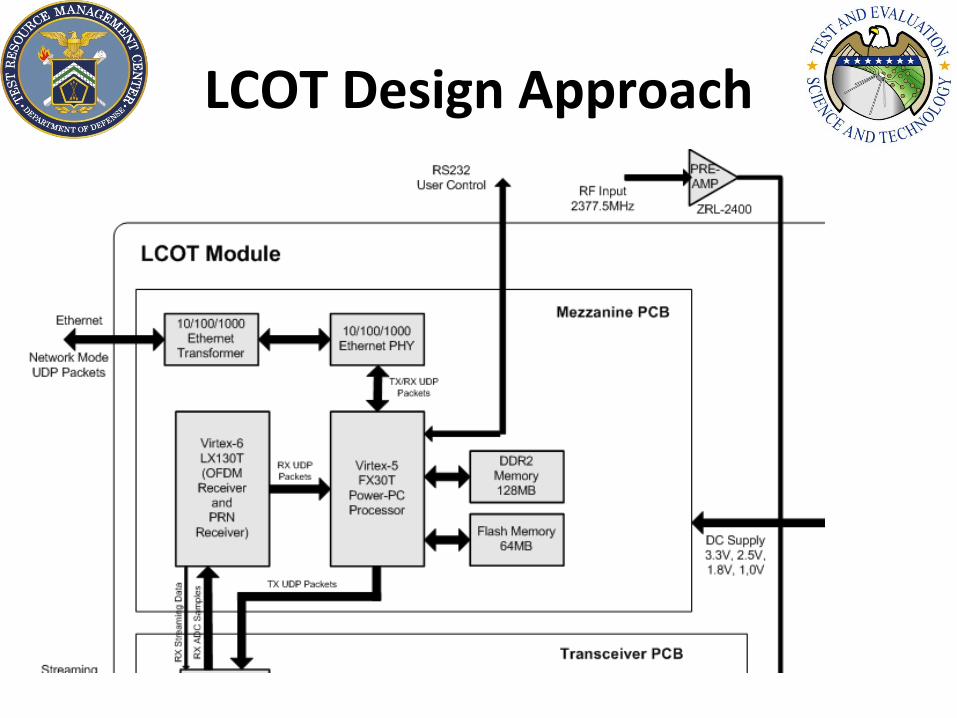
The LCOT module consists of the mezzanine section, transceiver, HPA module and DC/DC converter board. The interfaces between the various sections are shown in the system diagram in Figure 4.2 below. The main inputs are the RF input, the DC power input, the Ethernet, the RS232 control and the LVDS I/O. The main outputs are the RF output from the HPA and the LVDS outputs.
4.3 SUBSYSTEMS In this section, the individual subsystems for the LCOT module are described in detail. DC/DC CONVERTER: The LCOT is powered off two Vicor Converters. The PA DC converter is V24C28T100BL2. The 5V converter is V24C5H100BG2. These are shown in Figure 4.3 below. Voltage regulators are used on each subsidiary power line to supply individual voltages to the mezzanine, transceiver and HPA boards. The input power to the LCOT is 28V and 6A.
Figure 3.0: IEEE 802.11g Transmit Spectral mask for 20 MHz channel.

5
Figure 4.2: System diagram for the LCOT module.
Figure 4.3: Photograph of the DC/DC converters for the LCOT module.

6
TRANSCEIVER BOARD: The transceiver board is shown in Figure 4.4 below. The transmitter receives user data from the LVDS serial clock and data (streaming mode), the network UDP (network mode), or from the internal PRN generator (streaming mode). The Virtex-4 FPGA performs LDPC encoding and OFDM modulation of the received user data. The real (I) and imaginary (Q) components of the OFDM signal are converted into analog domain using two AD9772A DACs. The AD8346 modulator generates an S-Band (2200MHz) OFDM signal from the two I and Q analog signals. The S-Band signal is amplified to a medium power level (0-4dBm) for input to the high power amplifier module. On the receive side, the RF receive frequency is set to 2377.5MHz. This RF signal is fed through a pre-amp, ZRL-2400, and then through two stages of low noise -amplification. The HLX synthesizer mixes with the input RF frequency to down-convert to 70MHz. The AD8370 variable gain amplifier is part of the receiver AGC. Its gain is adjusted during OFDM short preamble period and then held constant for the remaining of the OFDM packet. The resulting down-converted signal is fed through to the ADC. The ADC feeds the digitized signal to the Virtex-4 FPGA and on to the Virtex-6 FPGA on the mezzanine for OFDM demodulation.
Figure 4.4: Photograph of the Transceiver board (RF side). MEZZANINE BOARD : The mezzanine board consists of Virtex-5 and Virtex-6 FPGAs. The Virtex-6 FPGA receives the digitized OFDM signal from the Virtex-4 FPGA on the transceiver board. The Virtex-6 FPGA performs demodulation and LDPC decoding of the OFDM signal. The recovered UDP packets are fed to the Virtex-5 FPGA for network output, whilst the recovered streaming data is fed to the Virtex-4 FPGA for LVDS serial clock and data output. The streaming data is also fed to the internal PRN receiver for BER calculation.

7
The Virtex-5 FPGA includes an embedded Power-PC processor that performs networking (TCP/UDP/IP) stack for LCOT. The processor also provides the user control interface through the UART port. The processor system diagram is shown in Figure 4.5 below. The processor clock speed is 400MHz whilst the system bus speed is 100MHz.
Figure 4.5: PowerPC 440 System Block Diagram
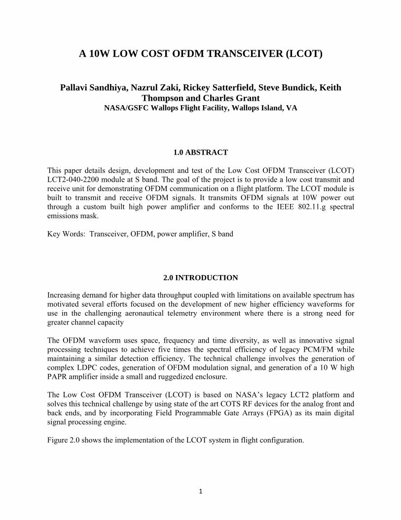
POWER AMPLIFIER : The devices used in the LCT2-040-2200 power amplifier module were GaN devices manufactured by Nitronex. These were seen to be the optimum choice in terms of available output power, bandwidth and efficiency. Three devices were used, NPTB00004, NPTB00050 and NPT25100, to form a three stage high power amplifier. The three stage LCOT power amplifier was simulated on ADS. The S parameters and nonlinear models for the transistor devices were obtained from Nitronex. The first stage was designed for maximum gain and good input return loss. The second stage was designed for flat gain. The third stage was designed for maximum power delivered to the load. All stages were designed to be unconditionally stable. The dimensions of the LCOT PA are 3.74 x 1.24 inches. The layout is shown below in Figure 4.6 along with a description of the various sections of the module.
8
5.0 TEST RESULTS
Measurements of the LCOT were taken in the lab at Edwards Air Force Base. A test transceiver was used to generate a two way link to test successful and error free demodulation of the received OFDM signal. In addition, the transmitted signal at 10W average output power met the IEEE 802.11g transmit spectral mask and data was received with no errors over the full dynamic range. Figure 5.1 shows a photograph of the LCOT module during testing. The small ruggedized enclosure is suitable for mounting on a flight platform. Figure 5.2 shows a plot of the OFDM transmitted signal captured on a spectrum analyzer at 10W average output power.
Figure 4.6: The four main components are shown: NPTB00004, NPTB00050, NPT25100 and the CAD215 circulator.

9
Figure 5.2 : Demonstration of Full Duplex streaming mode operation from Flight unit to
test transceiver. LCOT Flight unit output power at transmit port is at 10W
Figure 5.1: Photograph of the LCOT module (pre-amp not shown).

10
6.0 CONCLUSIONS
The LCOT unit meets the technical challenge of LDPC codes, generation of OFDM modulation signal, and transmission of 10 W high PAPR signal inside a small and ruggedized enclosure. The LCOT module achieves a low cost solution by using off-the-shelf RF devices for the analog front and back ends and also incorporates a Field Programmable Gate Array (FPGA) as its main digital signal processing engine. The 10W transmitted signal passes the IEEE 802.11g spectral mask specifications.
7.0 ACKNOWLEDGMENTS
The authors would like to thank the SET team at Edwards Air Force Base for the use of their lab equipment and facilities during testing.

Session B.2 Spectrum Efficient Technologies
GET CONNECTED to LEARN, SHARE, AND ADVANCE.
Track Chair: Mr. Tom Young
This project is funded by the Test Resource Management Center (TRMC) Test and Evaluation/Science & Technology (T&E/S&T) Program through the U.S. Army Program Executive Office for Simulation, Training, and Instrumentation (PEO STRI) under Contract No. MIPR1LO80W1599.
412TW-PA-12422 Distribution Statement A: Distribution is unlimited. Any opinions, findings and conclusions or recommendations expressed in this material are those of the author(s) and do not necessarily reflect the views of the Test Resource Management Center (TRMC) and Evaluation/Science & Technology (T&E/S&T) Program and/or the U.S. Army Program Executive Office for Simulation, Training, & Instrumentation (PEO STRI).
Approval: 412 TW-PA-12422

A 10W Low Cost OFDM Transceiver (LCOT)
Presenter : Dr. Pallavi Sandhiya LCOT Team : Steve Bundick, Nazrul Zaki, Rickey
Satterfield, Keith Thompson, Chuck Grant
05/16/2012
AFFTC

Outline of Presentation
• Introduction/Motivation • Specifications • LCOT System Design approach • Subsystems • Packaging and interface • Test Results • Conclusions

Introduction – Increasing demand for higher data throughput coupled with
limitations on available spectrum has motivated several efforts focused on the development of new higher efficiency waveforms for use in the challenging aeronautical telemetry environment.
– The OFDM waveform uses space, frequency and time diversity, as well as innovative signal processing techniques to achieve five times the spectral efficiency of legacy PCM/FM while maintaining a similar detection efficiency
– There is a strong need for greater channel capacity.

Introduction
– The technical challenge involves the generation of complex LDPC codes, generation of OFDM modulation signal, and generation of a 10 W high PAPR amplifier inside a small and ruggedized enclosure
– The NASA Low Cost TDRSS Transceiver (LCT2) platform solves this technical challenge by using state of the art COTS RF devices for the analog front and back ends, and by incorporating a Field Programmable Gate Array (FPGA) as its main digital signal processing engine.

Specifications Parameter Range Notes 1.0 Transmitter 1.1 RF Power Output 10W min. Matched load assumed 1.2 Output Impedance 50 Ω 1.4 Frequency Range 2200 MHz 1.5 Spurious Outputs > -20 dBr (at 11% of Fc), > -28 dBr (at 20% of
Fc), > -40 dBr ( within 50 MHz of Fc) Specified at 2.2GHz
2.0 Modulation Performance 2.1 Modulation Modes QPSK OFDM or 16-QAM OFDM Modulation mode
programmable 2.2 Data Rates < 15 Mbps QPSK, < 28 Mbps 16-QAM 3.0 Receiver 3.1 Center Frequency 2377.5 MHz 3.2 Input Impedance 50 Ω 3.3 Noise Figure < 2.5 dB 4.0 Power Interface 4.1 Input Voltage 28 VDC 4.2 Power 112 W, 4A (Receiver mode only)
154 W, 5.5A (Transmit & Receive)
5.0 User interfaces 5.1 RS232 control/status Serial Asynchronous UART 5.2 LVDS Serial Data Input/ Output
Interface VCM: 1.2V Diff Output Voltage Magnitude: 247mV/454mV min/max into 100Ω differential load.
Differential Data and clock
5.4 Ethernet UDP/IP Data Interface 10/100Base-T 6.0 Mechanical 5.5 "x 5" x2.25“, 3lbs

Flight Configuration
LCOT Flight Unit
LCOT Ground Unit
OFDM Transmission 110Km range at 27MB/s
TEST BER
LCOT Internal BER
2200 MHz
2377.5 MHz

OFDM Spectral Mask The LCOT module was required to transmit 10W and to conform to the IEEE 802.11.g transmit spectral mask.. IEEE defines the permitted distribution of signal power for each 802.11 layer amendment and to which the measured Spectral Mask must be compared
LCOT Design Approach

LCOT Design Approach

DC/DC Converter The LCOT is powered off two Vicor Converters. Voltage regulators are used on each subsidiary power line to supply individual voltages to the
mezzanine, transceiver and HPA boards.
The input power to the LCOT is 28V and 6A.

Transceiver Board The transmitter receives user data from the LVDS serial clock and data (streaming mode) or the network UDP (network mode). The Virtex-4 FPGA performs LDPC encoding and OFDM modulation of the received user data. The real (I) and imaginary (Q) components of the OFDM signal are converted into analog domain using an AD9772A DAC

Transceiver Board
On the Tx side the modulator generates an S-Band (2200MHz) OFDM signal from the two I and Q analog signals. The S-Band signal is amplified to a medium power level (0-4dBm) for input to the high power amplifier module.
On the Rx side, the RF receive frequency is set to 2377.5MHz. This RF signal is fed through a pre-amp and then through two stages of low noise -amplification. The HLX synthesizer mixes with the input RF frequency to down-convert to 70MHz and is fed to the receiver AGC. The resulting down-converted signal is fed through to the ADC and on to the Virtex-4, Virtex-6 FPGA on the mezzanine for OFDM demod.

Mezzanine Board The mezzanine board consists of Virtex-5 and Virtex-6 FPGAs. These perform demodulation and LDPC decoding of the OFDM signal.
The Virtex-5 FPGA includes an embedded Power-PC processor that performs networking (TCP/UDP/IP) stack for LCOT. The processor also provides the user control interface through the UART port.

Power amplifier module The LCOT power amplifier module consist of three Gallium nitride devices (GaN). These were seen to be the optimum choice in terms of available output power, bandwidth and efficiency. The PA runs off a 30V power supply and draws 3.8A

Power amplifier module
stage3
stage2
stage1
The three stage LCOT power amplifier was simulated on ADS using nonlinear models for the transistor devices The first stage was designed for maximum gain and good input return loss. The second stage was designed for flat gain. The third stage was designed for maximum power delivered to the load. All stages were designed to be unconditionally stable.

Power amplifier module The LCOT PA was driven from the signal generated by the transceiver board. The input OFDM signal to the PA has a total power of 4.86dBm. At 10W output power, the LCOT PA passes the IEEE 802.11g transmit spectrum mask.

Packaging and Interface

Bit rates
Modulation RATE Bit rate Streaming Mode 16-QAM 4/5 31.6Mbps
16-QAM 3/4 29.5Mbps 16-QAM 2/3 26.5Mbps 16-QAM 1/2 20.2Mbps
QPSK 4/5 16.2Mbps QPSK 3/4 15.2Mbps QPSK 2/3 13.6Mbps QPSK 1/2 10.3Mbps
UDP mode 16-QAM 4/5 30.2Mbps 16-QAM 3/4 28.2Mbps 16-QAM 2/3 25.3Mbps 16-QAM 1/2 19.3Mbps
QPSK 4/5 15.5Mbps QPSK 3/4 14.5Mbps QPSK 2/3 13.0Mbps QPSK 1/2 9.8Mbps
Below are the maximum bit rates achievable for all modulations and with Inter-frame time interval set to 0.0us.

Transmission Spectrum
•Demonstration of Full Duplex streaming mode operation from Flight unit to test transceiver .
•Plot shows LCOT Flight unit calibrated output power at transmit port at 10W

Receive on test setup
•Demonstration of Full Duplex streaming mode operation from Flight unit to test transceiver
•Plot shows test transceiver receive port.

Receive on Flight unit
•Demonstration of Full Duplex streaming mode operation from Flight unit to test transceiver.
•Plot shows receive port of flight unit.

Conclusions
• The LCOT unit meets the technical challenge of LDPC codes, generation of OFDM modulation signal, and transmission of 10 W high PAPR signal inside a small and ruggedized enclosure
• The LCOT platform uses state of the art COTS RF devices for the analog front and back ends, incorporates a Field Programmable Gate Array (FPGA) as its main digital signal processing engine.
•The 10W transmitted signal passes the IEEE 802.11g spectral mask specifications

QUESTIONS?