a 130 nm operational amplifier: design and schematic level ... · keywords–cmos, integrated...
TRANSCRIPT
A 130 nm Operational Amplifier: Design and Schematic Level Simulation
Aleksandar PajkanovicFaculty of Technical Sciences
University of Novi [email protected]
Abstract—In this paper an operational amplifier of generalpurpose is presented. The unified current-control model isused to synthesize a standard, two-stage topology based circuit.The design procedure is discussed thoroughly and every stepis explained in details. The results obtained include openloop gain of 74 dB, the gain-bandwidth product of 100 MHzand the phase margin higher than 46◦. Supply voltage andtemperature coefficients are analyzed and discussed withinthe paper. Process variations are investigated through corneranalysis. The results presented are obtained through schematiclevel simulations using the Spectre Simulator from CadenceDesign System and a standard 130 nm CMOS technologyprocess.
Keywords–CMOS, integrated circuits, op amp design, unifiedcurrent-control model, schematic level simulations
I. INTRODUCTION
The operational amplifier represents one of the mostuseful and one of the most used building blocks for analogintegrated circuits. Even though it was established 80 yearsago, by Harry Black [1], the fundamental idea remains thesame: to make an amplifier stable over temperature changesand power-supply variations, we build an extremely highgain amplifier and introduce it in the negative feedbackconfiguration.
The term operational amplifier (op amp) was used for thefirst time in 1947, in [2] where certain applications of thecircuit were also presented. In the following two decades, opamps became more and more popular with the developmentof the bipolar integrated circuits technology [3]. The firstcomprehensive study of the op amps circuit was givenby Solomon in [4]. During more than half a century ofdevelopment, the op amp has been used in a variety of ap-plications, such as: instrumentation amplifiers, continuous-time and switched capacitor filters, D/A and A/D converters,non-linear analog operators, signal generators and voltageregulators [5], [6], [7].
In this paper, the design and synthesis of a two-stagefrequency compensated op amp are performed using theunified current-control model (UICM) [7], [8]. Open loopgain achieved at nominal conditions is 74 dB, whereas phasemargin and gain-bandwidth product are 46◦and 100 MHz,respectively. Process, voltage and temperature (PVT) vari-ations and stability are also analyzed within this paper.Simulations are performed using the Cadence Design Systemtoolchain a standard 130 nm CMOS technology process.
II. MODEL USED
The design methodology is based on the UICMmodel [7], [8]. It is a current-based MOSFET model thatuses the concept of inversion level. According to the UICMmodel, the drain current can be split into the forward (IF )and reverse (IR) currents:
ID = IF − IR = IS(if − ir), (1)
where IS is the normalization specific current, and if and irare inversion levels, forward and reverse, respectively. Theforward and reverse currents depend on the gate to sourceand gate to drain voltages, respectively. If the transistoroperates in saturation, we have:
IF � IR, thus: ID ≈ IF = IS · if . (2)
The normalization current is a function of the technology:
IS =μCoxφ2
T n
2
W
L, (3)
where μ represents the charge mobility, Cox gate-oxidecapacitance per area, φT thermal voltage, n slope factor andW/L transistor aspect ratio.
The inversion level value signifies the transistor operationregion in the following way: if if < 1, the transistoroperates in weak inversion and if if > 100 the transistoroperates in strong inversion region. If 1 < if < 100, thetransistor operates in moderate inversion region. The voltageand current are related in the following manner [7]:
VP − VS(D)
φT
=√
1 + if(r)−3+ln(√
1 + if(r) − 1)
, (4)
where VP is the pinch-off voltage, given as the differenceof the gate potential and the zero bias threshold voltage(modified by the slope factor):
VP ≈VG − VT0
n, if VG ≈ VT0. (5)
Transistor drain-source saturation voltage is calculated as:
VDSsat = φT
(√1 + if + 3
), (6)
while the transconductance is given as:
gm =2ID
nφT
(√1 + if + 1
) . (7)
Further detailed description of the model can be foundin [7] and [8].
7th International Conference on Computational Intelligence, Communication Systems and Networks (CICSyN)
978-1-4673-7016-5/15 $31.00 © 2015 IEEE
DOI 10.1109/CICSyN.2015.50
212
7th International Conference on Computational Intelligence, Communication Systems and Networks (CICSyN)
978-1-4673-7016-5/15 $31.00 © 2015 IEEE
DOI 10.1109/CICSyN.2015.50
212
7th International Conference on Computational Intelligence, Communication Systems and Networks (CICSyN)
978-1-4673-7016-5/15 $31.00 © 2015 IEEE
DOI 10.1109/CICSyN.2015.50
249
7th International Conference on Computational Intelligence, Communication Systems and Networks (CICSyN)
978-1-4673-7016-5/15 $31.00 © 2015 IEEE
DOI 10.1109/CICSyN.2015.50
249
7th International Conference on Computational Intelligence, Communication Systems and Networks (CICSyN)
978-1-4673-7016-5/15 $31.00 © 2015 IEEE
DOI 10.1109/CICSyN.2015.50
249
7th International Conference on Computational Intelligence, Communication Systems and Networks (CICSyN)
978-1-4673-7016-5/15 $31.00 © 2015 IEEE
DOI 10.1109/CICSyN.2015.50
249
7th International Conference on Computational Intelligence, Communication Systems and Networks (CICSyN)
978-1-4673-7016-5/15 $31.00 © 2015 IEEE
DOI 10.1109/CICSyN.2015.50
249
7th International Conference on Computational Intelligence, Communication Systems and Networks (CICSyN)
978-1-4673-7016-5/15 $31.00 © 2015 IEEE
DOI 10.1109/CICSyN.2015.50
249
III. THE PROPOSED CIRCUIT THEORY OVERVIEW
One way to increase the voltage gain of a single-stageamplifier is to use cascode topology, since in this waythe output impedance is increased. Such an approach alsoimplies stacked transistors (telescopic and folded cascodetopologies [7]), which means that the output swing andthe overdrive voltage are reduced. This issue is even moresignificant when advanced technology nodes are in question,since the supply voltage also scales. A possible solutionis to use cascaded stages instead. Such comfort is paid byintroducing another pole in the system, which appears as aconsequence of the second amplifying stage. Another pole inthe system, if not handled properly, can put in question thecircuit transient response. Therefore, a part of the two-stageop amp design is the task of frequency compensation.
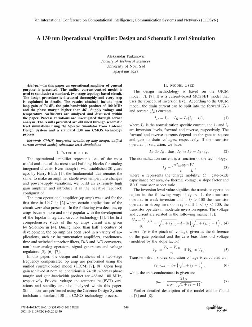
The proposed circuit schematic is shown in Fig. 1. Thetopology is standard and commonly used and it consists of adifferential amplifier (first stage), a common source amplifier(second stage) and the frequency compensating network. Inthis case, the compensating network consists only of thefeedback capacitor, CC . The detailed discussion and the fullexplanation of the frequency compensation technique andthe Miller effect are beyond the scope of this paper, andhere only a short overview is given.
Frequency compensation is generally required in a two-stage op amp in order to avoid the op amp in a feedbackconfiguration being unstable or having an unacceptablyunder-damped oscillatory time response. Namely, for thestability of the feedback amplifier a necessary conditionis that the phase delay introduced by the open-loop gainand the feedback network at the unity-gain frequency doesnot exceed 180◦. In other words, to obtain a time responsewithout excessive overshoot, a phase margin (PM) of 45◦isneeded [6]. An op amp characterized by such a feature willbe stable, i.e. will not oscillate when connected in feedbackconfiguration.
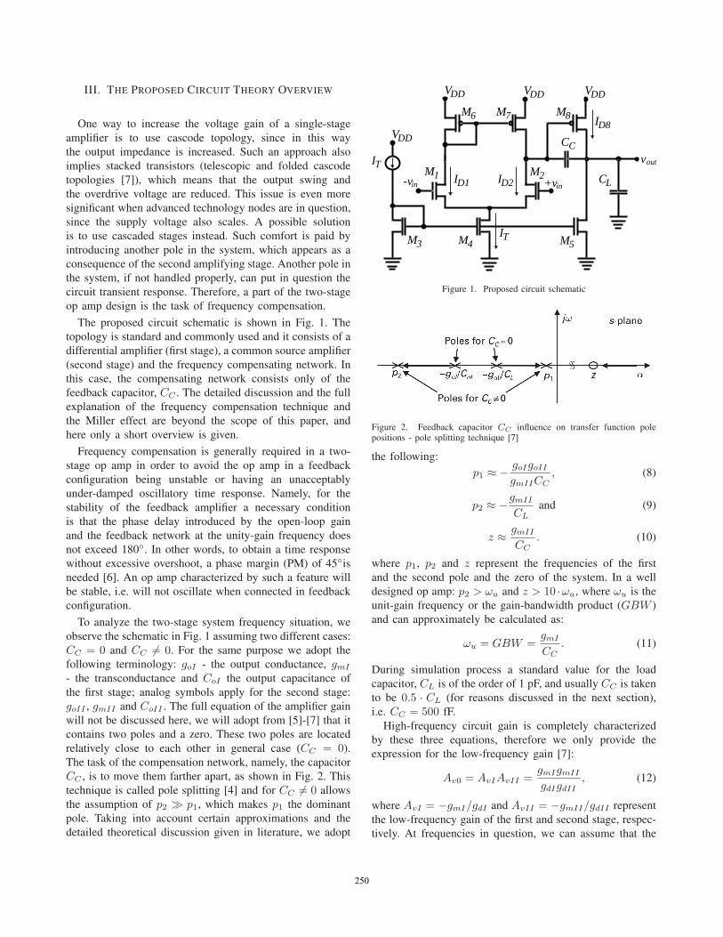
To analyze the two-stage system frequency situation, weobserve the schematic in Fig. 1 assuming two different cases:CC = 0 and CC �= 0. For the same purpose we adopt thefollowing terminology: goI - the output conductance, gmI
- the transconductance and CoI the output capacitance ofthe first stage; analog symbols apply for the second stage:goII , gmII and CoII . The full equation of the amplifier gainwill not be discussed here, we will adopt from [5]-[7] that itcontains two poles and a zero. These two poles are locatedrelatively close to each other in general case (CC = 0).The task of the compensation network, namely, the capacitorCC , is to move them farther apart, as shown in Fig. 2. Thistechnique is called pole splitting [4] and for CC �= 0 allowsthe assumption of p2 � p1, which makes p1 the dominantpole. Taking into account certain approximations and thedetailed theoretical discussion given in literature, we adopt
��� ��� ���
����
�� ��
���� �� ��
��
���
��� �
�� �� ��
��
���� ���� ��
Figure 1. Proposed circuit schematic
Figure 2. Feedback capacitor CC influence on transfer function polepositions - pole splitting technique [7]
the following:p1 ≈ −
goIgoII
gmIICC
, (8)
p2 ≈ −gmII
CL
and (9)
z ≈gmII
CC
. (10)
where p1, p2 and z represent the frequencies of the firstand the second pole and the zero of the system. In a welldesigned op amp: p2 > ωu and z > 10 ·ωu, where ωu is theunit-gain frequency or the gain-bandwidth product (GBW )and can approximately be calculated as:
ωu = GBW =gmI
CC
. (11)
During simulation process a standard value for the loadcapacitor, CL is of the order of 1 pF, and usually CC is takento be 0.5 · CL (for reasons discussed in the next section),i.e. CC = 500 fF.
High-frequency circuit gain is completely characterizedby these three equations, therefore we only provide theexpression for the low-frequency gain [7]:
Av0 = AvIAvII =gmIgmII
gdIgdII
, (12)
where AvI = −gmI/gdI and AvII = −gmII/gdII representthe low-frequency gain of the first and second stage, respec-tively. At frequencies in question, we can assume that the
213213250250250250250250

following is valid [7]:
gmI ≈ gm1 gdI ≈ gd2 + gd6
gmII ≈ gm8 gdII ≈ gd5 + gd8(13)
where gm1 and gm8 represent the transconductances oftransistors M1 and M8, and gd2, gd5, gd6 and gd8 representthe output conductances of transistors M2, M5, M6 and M8.
IV. OP AMP DESIGN USING UICM
Before employing the UICM to design the op amp, certainvalues need to be assumed. Short-channel effects severelyaffect transistor operation in advanced technology nodes [9],where 130 nm belongs. This technology intrinsic frequencylimit is of the order of 100 GHz at minimum channellengths. Since this circuit is intended for applications ofthe order of MHz, it is not mandatory to use minimumchannel length. This means that we have the liberty touse larger channel lengths, so that the short-channel effectsare not dominant. Therefore, in this paper Lmin = 500nm. Further, we assume the minimum transistor width,because the mismatch is inversely proportional to the devicesize [10]. In order to improve device matching, we determinethat no transistor channel width should be smaller than tentimes the minimum assumed length: wmin = 5 μm. For thetransistor model in use, the nominal voltage is VDD = 3.3V. All transistors must operate in saturation (if � ir) andthe drain-source saturation voltages are of the order of 0.3V. For the simplicity of calculations, we assume that theinversion level is the same for all transistors in the circuit.
Using the transistor model approximate parameters, it ispossible to calculate the sheet normalization current for n-channel:
ISHN =ISN
W/L=
μNCoxφ2T n
2= 61 nA, (14)
and for p- channel devices:
ISHP =ISP
W/L=
μP Coxφ2T n
2= 13.4 nA. (15)
Since it directly defines the transistor working point,we first calculate the inversion level. Taking into accountequations given in section II of this paper and the schematicin Fig. 1, the easiest way to obtain the inversion level isto assume VDSsat4 = 0.3 V for transistor M4and applyequation (6):
if =
(VDSsat4
φT
− 3
)2
− 1 = 73.44 ≈ 80. (16)
Therefore, the transistors operate in moderate inversion.Next, we determine the tail current, i.e. ID4, the drain
current of M4. In order to do so we notice that ID4 =ID1 + ID2 = 2 · ID1 and actually first calculate ID1 usingequation (7):
ID1 = ID2 =gm1nφT
2
(√(if + 1) + 1
). (17)
The unknown value of gm1 is obtained using equations (11)and (13) as:
gm1 = ωu · CC = 2π · 100 · 106 · 500 · 10−15 =
= 314 · 10−6 ≈ 350μS, (18)
where a bit higher transconductance value is taken to guaran-tee the needed performance. Using (18) in (17), we obtainID1 = 44.56 μA ≈ 45 μA, which enables us to find thegeometry ratios of transistors M1 and M2:(
W
L
)1
=
(W
L
)2
=ID1
ISHN if= 9.53 ≈ 10. (19)
Since Lmin = 500 nm, we write: W1 = W2 = 5 μm.Keeping in mind, ID4 = 2·ID1, it follows W4 = 2·W1 = 10μm.
From Fig. 1, we see that ID6 = ID7 = ID1. Thisconclusion, along equation (15) enables the M6 and M7
geometry calculation as follows:(W
L
)6
=
(W
L
)7
=ID1
ISHP if= 41.97 ≈ 42, (20)
which further means that W6 = W7 = 21 μm.Since transistor M3 should be identical to M4, we now
have all the information needed to simulate the op amp firststage - the differential amplifier. This is done to check thetransistors DC operating points. Running the simplest DCsimulation, we find that the M1 operating point is a bitdifferent, but acceptable: ID1 = 46 μA and gm1 = 360μS. We also check the DC gain by reading the outputconductance values and using equations (12) and (13:
AvI =gm1
gd2 + gd7=
360
1.83 + 4.40≈ 58. (21)
where minus sign is omitted since it represents only the180◦phase shift. This gain magnitude does not satisfy thestarting requirement of Av0 =74 dB, where the first stageshould provide the gain of 37 dB, i.e. 70. Since the mainpurpose of the PMOS transistors, M6 and M7, is to act asloads and that their output conductance directly influencesthe DC gain - we will improve AvI by decreasing gd7. Thetransistor output conductance is inversely proportional to thechannel length. Therefore, to obtain an acceptable level ofgain in the first stage, we increase the M6 and M7 channellengths to L6 = L7 = 600 nm and adopt the new valuesof channel widths accordingly: W6 = W7 = 28.6 μm.Rerunning the DC simulation, we find AvI = 36.52 dBwhich is acceptable.
The second stage transistor operating points and geome-tries we derive from the phase margin requirement. The PMis actually the difference in phase of the output and the inputsignal at ωu frequency. Since this circuit transfer function ischaracterized by a zero and two poles, phase difference ofoutput and input is:
PM (ω) = tan−1(ω
z
)−tan−1
(ω
p1
)−tan−1
(ω
p2
). (22)
214214251251251251251251
Since we are interested in the value of PM at ω = ωu, weuse equations (8)-(11) to obtain:
PM (ωu) = tan−1
(ωu
10 · ωu
)−
− tan−1
(gmI
CC
·gmIICC
gdIgdII
)− (23)
− tan−1
(ωu
p2
).
The first member of this equation is 0.1 and the second oneis, according to (12), the op amp DC gain, Av0. Assumingthat Av0 = 74 dB as required and remembering (13), wewrite:
PM (ωu) = 84.29◦ − tan−1
(ωu
p2
)≥ 45◦ (24)
which further yields: p2 ≥ 1.22 · ωu. Equations (10), (11)and (24) provide us with the conditions:
gm8 ≥ 10 · gm1 and CC ≥ 0.13CL. (25)
The first condition we match by setting gm8 = 3.5 mS,while the second one is already fulfilled. Applying (17)to M8, we obtain its drain current: ID8 = ID5 = 465μA, which, using (15) and (19) further yields the geometryratio: W8/L8 = 434 μm. According to (12) and (13), gd8
decisively influences the second stage gain, so we keepthe channel length modification, i.e. L8 =600 nm andW8 = 260.4 μm. The M5 is calculated in the same manner:W5 = 48 μm.
Finally, all the circuit components are calculated and theDC simulation of the op amp yields promising values:
AvII =gm2
gd5 + gd8=
3400
14.63 + 35.37≈ 68 = 37 dB. (26)
Running a simple AC analysis, we find that Av0 of around74 dB and PM of 53◦are satisfactory, but that ωu is only80 MHz. The easiest change that we can make to the circuit,without affecting the transistor operation points is to vary theCC . According to condition (25), we can make CC as low as130 fF. Even though decreasing its capacitance does increaseωu, this procedure also decreases the PM, e.g. at CC =200 fF, ωu = 110 MHz but PM = 39◦. Therefore, wemust turn to the first condition in (25) and further increasegm8/gm1 ratio, e.g. gm8 = 12 ·gm1. In this case, the secondstage transistor geometries are: (W8/L8) = (312.6 μm / 600nm) and (W5/L5) = (57.5 μm / 500 nm).
After some fine tuning through the feedback capacitorvariation, we find that the requirements of 74 dB, 100 MHzand 46◦in the nominal case are fulfilled for the capacitorvalue of CC=290 fF. Such performance is paid by powerconsumption of 2.61 mW for a supply voltage of 3.3 V.
V. SIMULATION RESULTS
In Fig. 3 the op amp in open loop configuration ACsimulation results are given. As designed in section IV, thecircuit shows the fulfillment of the given requirements in thenominal conditions, i.e. at room temperature, supply voltageof 3.3 V and using the transistor model of typical values.The unity-gain frequency, ωu = 2π · fu is 2π·100 MHz,while the DC gain is 73.91 dB and PM is 46◦. Further, theop amp transfer function poles and zero are also shown.The dominant pole, p1, is the one which introduces thegain decrease of -20 dB per decade and the phase shift of90◦, marked as 3 dB frequency in the figure. The secondpole introduces the additional -20 dB per decade to thegain decrease at frequency of 210 MHz. Obviously it isbeyond fu, which means that we successfully employed thefrequency compensation technique through the feedback ca-pacitor CC to remove its influence on the op amp operationat frequencies of interest. The zero is shown at frequencyof beyond 2 GHz. Therefore, both conditions mentioned insection III theory discussion, p2 > ωu and z > 10 · ωu arefulfilled.
For the input signal amplitude of 1 μV and frequency of20 kHz, both input and output are shown in Fig. 4. Thecircuit introduces a time delay of 4.4 μs. From Fig. 5 weconclude that the op amp output takes an interval of 65 μto settle.
In Tab. I process, voltage and temperature (PVT) vari-ations influences to the op amp characteristics are shown.Process variations are analyzed through running the sim-ulations with different component nodes. Namely, the DCcurrent ideal source shown in Fig. 1 is actually replaced by aresistor model available for the 130 nm technology process.Also, the process variations of the feedback capacitor areincluded in the worst case analysis. Voltage variations areintroduced by setting the supply voltage to ±10 % values ofthe nominal, i.e. 2.97 V and 3.63 V. Temperature influenceis analyzed by varying the temperature over the whole rangefor which the technology models are valid, namely -40◦upto 125◦.Besides these simulations performed with the op amp
in the open loop configuration, the stability analysis isperformed for the nominal case. For this simulation, the opamp is connected in the closed loop configuration with unityfeedback. This stability simulation purpose is to show thecircuit’s behavior when the loop is closed and determinewhether there is a possibility to oscillate. The op ampdesigned in this paper, because of all the precautions takenand careful calculations in section IV does not oscillate andthe characteristics for this configuration are given in Tab. I.
Important characteristics of an op amp also include:common-mode rejection ratio (CMRR), power supply re-jection ratio (PSRR), input common mode range (ICMR−and ICMR+), output range (VOmax and VOmin) and slew
215215252252252252252252
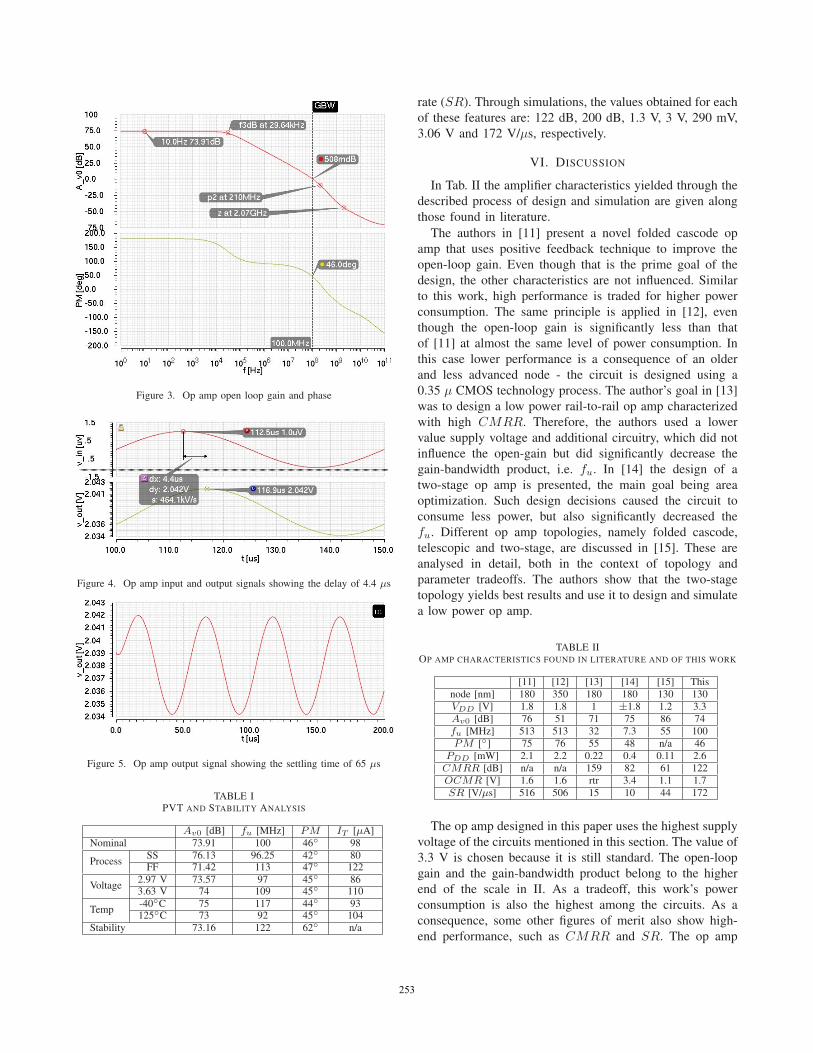
Figure 3. Op amp open loop gain and phase
Figure 4. Op amp input and output signals showing the delay of 4.4 μs
Figure 5. Op amp output signal showing the settling time of 65 μs
TABLE IPVT AND STABILITY ANALYSIS
Av0 [dB] fu [MHz] PM IT [μA]Nominal 73.91 100 46◦ 98
ProcessSS 76.13 96.25 42◦ 80FF 71.42 113 47◦ 122
Voltage2.97 V 73.57 97 45◦ 863.63 V 74 109 45◦ 110
Temp-40◦C 75 117 44◦ 93125◦C 73 92 45◦ 104
Stability 73.16 122 62◦ n/a
rate (SR). Through simulations, the values obtained for eachof these features are: 122 dB, 200 dB, 1.3 V, 3 V, 290 mV,3.06 V and 172 V/μs, respectively.
VI. DISCUSSION
In Tab. II the amplifier characteristics yielded through thedescribed process of design and simulation are given alongthose found in literature.
The authors in [11] present a novel folded cascode opamp that uses positive feedback technique to improve theopen-loop gain. Even though that is the prime goal of thedesign, the other characteristics are not influenced. Similarto this work, high performance is traded for higher powerconsumption. The same principle is applied in [12], eventhough the open-loop gain is significantly less than thatof [11] at almost the same level of power consumption. Inthis case lower performance is a consequence of an olderand less advanced node - the circuit is designed using a0.35 μ CMOS technology process. The author’s goal in [13]was to design a low power rail-to-rail op amp characterizedwith high CMRR. Therefore, the authors used a lowervalue supply voltage and additional circuitry, which did notinfluence the open-gain but did significantly decrease thegain-bandwidth product, i.e. fu. In [14] the design of atwo-stage op amp is presented, the main goal being areaoptimization. Such design decisions caused the circuit toconsume less power, but also significantly decreased thefu. Different op amp topologies, namely folded cascode,telescopic and two-stage, are discussed in [15]. These areanalysed in detail, both in the context of topology andparameter tradeoffs. The authors show that the two-stagetopology yields best results and use it to design and simulatea low power op amp.
TABLE IIOP AMP CHARACTERISTICS FOUND IN LITERATURE AND OF THIS WORK
[11] [12] [13] [14] [15] Thisnode [nm] 180 350 180 180 130 130VDD [V] 1.8 1.8 1 ±1.8 1.2 3.3Av0 [dB] 76 51 71 75 86 74fu [MHz] 513 513 32 7.3 55 100PM [◦] 75 76 55 48 n/a 46
PDD [mW] 2.1 2.2 0.22 0.4 0.11 2.6CMRR [dB] n/a n/a 159 82 61 122OCMR [V] 1.6 1.6 rtr 3.4 1.1 1.7SR [V/μs] 516 506 15 10 44 172
The op amp designed in this paper uses the highest supplyvoltage of the circuits mentioned in this section. The value of3.3 V is chosen because it is still standard. The open-loopgain and the gain-bandwidth product belong to the higherend of the scale in II. As a tradeoff, this work’s powerconsumption is also the highest among the circuits. As aconsequence, some other figures of merit also show high-end performance, such as CMRR and SR. The op amp
216216253253253253253253
phase margin is at the lower limit of acceptability, but stillgood enough as proven in section IV. This circuit is designedwith no application as a goal, but it is of a general purpose.Once it is applied to a specific task, the tradeoffs can beoptimized.
The parameters and the whole Tab. II are in no way adirect one-on-one comparison between the designed circuitsand in no mean are given to claim that one or another op ampis better or worse. As discussed in the previous passage, allof the circuits mentioned, including the one developed in thispaper, are designed with different ideas of their respectiveauthors and therefore show different characteristics. Thepurpose of Tab. II is only to show that the results yielded bythe design process presented in sections III-V of this paperare of the order of magnitude found in recent literature.
VII. CONCLUSION
The op amp designed and simulated in this paper satisfiesthe initial requirements of 74 dB DC gain, 100 MHz gain-bandwidth product and 46◦of phase margin in nominalconditions. The combination of calculations using the UICMmodel and Spectre Simulator from Cadence Design Systemsallows quite straightforward and clear circuit synthesis pro-cess.
Stability analysis shows that the op amp developed is notsubject to oscillations when in closed loop configurations.This characteristic is ensured through careful design whilefulfilling all the conditions predefined through the theorydiscussion provided within the paper.
PVT variations analysis shows that the circuit is suscep-tible to these influences, but never failing for more than 8 %of the nominal case. Additional simulations performed giveinsight in more important op amp features, such as CMRRand PSRR, all of which are also satisfying.
In future work, the first step is the circuit layout throughwhich special attention is to be dedicated to process andmismatch variations. Temperature and voltage variations arealso to be improved. High performance set by the initialrequirements is accompanied by somewhat higher powerconsumption. When this op amp is applied to a specific task,there might be room for the optimization of this trade-off.
ACKNOWLEDGMENT
This work is funded from the European Union’s SeventhFramework Program for research, technological develop-ment and demonstration under grant agreement no. 289481- project SENSEIVER.
REFERENCES
[1] R. Mancini, Op Amps For Everyone. Texas Instruments, 2002.[2] J. Ragazzini, R. Randall, and F. Russell, “Analysis of problems in
dynamics by electronic circuits,” Proceedings of the IRE, vol. 35,no. 5, pp. 444–452, 1947.
[3] T. H. Lee, “Tales of the continuum: A subsampled history of analogcircuits,” Solid-State Ciruit Society Newsletter, vol. Fall, pp. 38–51,2010.
[4] J. Solomon, “The monolithic op amp: A tutorial study,” IEEE Journalof Solid-State Circuits, vol. 9, no. 6, pp. 314–332, 1974.
[5] B. Razavi, Design of Analog CMOS Integrated Circuit. McGraw-Hill, 2001.
[6] P. Allen and D. Holberg, CMOS Analog Circuit Design, 2nd. OxfordUniversity Press, 2002.
[7] M. C. Schneider and C. Galup-Montoro, CMOS Analog Design UsingAll-Region MOSFET Modeling. Cambridge University Press, 2010.
[8] A. I. A. Cunha, M. C. Schneider, and C. Galup-Montoro, “An mostransistor model for analog circuit design,” IEEE Journal of Solid-State Circuits, vol. 33, no. 10, pp. 1510–1519, 1998.
[9] Y. Tsividis and C. McAndrew, Operation and Modeling of the MOStransistor, 3rd Ed. Oxford University Press, 2011.
[10] P. Kinget, “Device mismatch and tradeoffs in the design of analogcircuits,” IEEE Journal of Solid-State Circuits, vol. 40, no. 6, pp.1212–1224, 2005.
[11] S. Farahmand and H. Shamsi, “Positive feedback technique for dc-gain enhancement of folded cascode op-amps,” in New Circuits andSystems Conference (NEWCAS), 2012 IEEE 10th International, 2012,pp. 261–264.
[12] A. Dadashi, S. Sadrafshari, K. Hadidi, and A. Khoei, “An enhancedfolded cascode op-amp using positive feedback and bulk amplificationin 0.35 um cmos process,” Analog Integrated Circuits and SignalProcessing, vol. 67, no. 2, pp. 2535–2542, 2010.
[13] T. Thongleam, S. Suwansawang, and V. Kasensuwan, “Low-voltagehigh gain, high cmrr and rail-to-rail bulk-driven op-amp using feed-forward technique,” in Communications and Information Technologies(ISCIT), 2013 13th International Symposium on, Sept 2013, pp. 596–599.
[14] K. Raut, R. Kshirsagar, and A. Bhagali, “A 180 nm low powercmos operational amplifier,” in Computational Intelligence on Power,Energy and Controls with their impact on Humanity (CIPECH), 2014Innovative Applications of, Nov 2014, pp. 341–344.
[15] M. Hamzah, A. Jambek, and U. Hashim, “Design and analysis ofa two-stage cmos op-amp using silterra’s 0.13 um technology,” inComputer Applications and Industrial Electronics (ISCAIE), 2014IEEE Symposium on, April 2014, pp. 55–59.
217217254254254254254254