a 20-ghz 130-nm cmos front-end using baluns on glass...
TRANSCRIPT

LUND UNIVERSITY
PO Box 117221 00 Lund+46 46-222 00 00
A 20-GHz 130-nm CMOS Front-End using Baluns on Glass Carrier
Törmänen, Markus; Sjöland, Henrik
Published in:Proc. 2008 IEEE 2nd International Conference on Signals, Circuits & Systems
Published: 2008-01-01
Link to publication
Citation for published version (APA):Törmänen, M., & Sjöland, H. (2008). A 20-GHz 130-nm CMOS Front-End using Baluns on Glass Carrier. InProc. 2008 IEEE 2nd International Conference on Signals, Circuits & Systems (pp. 138-141)
General rightsCopyright and moral rights for the publications made accessible in the public portal are retained by the authorsand/or other copyright owners and it is a condition of accessing publications that users recognise and abide by thelegal requirements associated with these rights.
• Users may download and print one copy of any publication from the public portal for the purpose of privatestudy or research. • You may not further distribute the material or use it for any profit-making activity or commercial gain • You may freely distribute the URL identifying the publication in the public portalTake down policyIf you believe that this document breaches copyright please contact us providing details, and we will removeaccess to the work immediately and investigate your claim.

Download date: 15. Jul. 2018

A 20-GHz 130-nm CMOS Front-Endusing Baluns on Glass Carrier
Markus TormanenDepartment of Electrical and Information Technology
Lund University, Box 118, 221 00 Lund Sweden
Email: [email protected]
Henrik SjolandDepartment of Electrical and Information Technology
Lund University, Box 118, 221 00 Lund Sweden
Email: [email protected]
Abstract—A 20-GHz 130-nm CMOS front-end using baluns onglass carrier is presented. The front-end consists of a CMOS diefeaturing a differential two-stage LNA, a passive double balancedmixer, and output buffers, which is flip-chipped on a glass carrierwhere baluns are realized for the RF and LO signals. The front-end measures a conversion gain of 11 dB, a noise figure of 7 dB,a 60 dB LO to RF isolation, an ICP1dB of -16 dBm, an IIP3 of-5.2 dBm, and an IIP2 of +34.5 dBm. The power consumption,excluding output buffers, is 38 mW. Furthermore, the RF inputis well protected as it can withstand a simulated 3 kV HBM ESDevent.
I. INTRODUCTION
The evolution of high data rate wireless communica-
tion systems has increased the demand for more band-
width, which can be fulfilled by employing more and wider
bands at higher frequencies for communications. The scal-
ing of CMOS has now made it a viable technology for
high frequency cost sensitive consumer applications. Pub-
lications have demonstrated high performance CMOS re-
ceiver front-ends at 60 GHz [1], and 24 GHz [2].
Differential receiver topologies are known to have higher
linearity and a higher degree of stability compared to single-
ended topologies, at the expense of higher power consump-
tion. These properties were reported already 1965 [3]. A disad-
vantage of differential topologies is that the antenna signal typ-
ically is single-ended, and that a balun then is needed to con-
vert it to differential form. To achieve good noise perfor-
mance the balun must have low losses, which makes it dif-
ficult to realize on chip.
This paper presents measurement results of a front-end using
a differential topology for increased linearity, and capacitive
cross-coupling for increased LO to RF isolation. The CMOS
die is flip-chipped on a glass carrier, where low loss baluns
are realized for the RF and LO input signals.
II. CIRCUIT DESIGN
The block schematic of the front-end is shown in Fig. 1.
It consists of a differential two-stage LNA, a passive double
balanced mixer, and open drain output buffers. The baluns on
the glass carrier, to generate the differential RF and LO input
signals, are also shown in the figure.
The first stage of the LNA is an inductively degen-
erated common-source stage with a cascode device as
IF+
IF-
LO
RF
Fig. 1. Front-end block schematic
shown in Fig. 2. This topology provides good input match-
ing, a low noise figure, and high reverse isolation. To fur-
ther increase the differential isolation, a capacitive cross-
coupling technique is used. Capacitors C1 and C2 form volt-
age dividers used to feed part of the output signal to the gate
of the opposite cascode devices. By setting the voltage divi-
sion ratio correctly, the currents due to the drain-source con-
ductance of the cascode devices can be cancelled for differ-
ential signals. Techniques like this will become more impor-
tant when the MOS transistors are scaled to shorter chan-
nel lengths, since the drain-source conductance then in-
creases. Spiral shunt inductors, Lsh, are used at the input to res-
onate with the capacitances of the pad and the flip-chip
bump. The shunt inductors also provide good ESD protec-
tion to the input transistor gates. The gate inductance, Lg, is re-
alized by two wires close to each other, and a small loop,
which can be seen in the die photograph, Fig. 11. Dif-
ferential inductors are used to provide inductive degenera-
tion, Ls, and to resonate the output, La. The ouput of the
first stage is loaded by the input impedance of the sec-
ond stage of the LNA.
The second stage of the LNA is a differential common-
source stage with cascode devices and capacitive cross-
coupling, as shown in Fig. 3. The output is resonated by a dif-
ferential inductor, Lb, and is also loaded by the in-
put impedance of the mixer.
Having a two-stage LNA provides sufficiant gain for a pas-
sive mixer to be used. In this circuit, a double-balanced pas-
sive mixer is used. To enable measurements, open-drain buffers
designed to drive 50 Ω loads are connected to the ouputs
of the mixer. The mixer and open-drain buffers are shown
in Fig. 4. The RF signal is AC-coupled to the mixer, pre-
2008 International Conference on Signals, Circuits and Systems
978-1-4244-2628-7/08/$25.00 ©2008 IEEE -1-

Vb Vb
Va Va
in+ in-
La/2 La/2
Ls/2 Ls/2Lg Lg
Lsh
C1
C1C2 C2
Lsh
out- out+
Fig. 2. First stage of the LNA
Vd Vd
Vc Vc
in+ in-
Lb/2 Lb/2
C1
C1C2 C2
out- out+
Fig. 3. Second stage of the LNA
venting DC-current, and setting the DC-voltage to zero
through 40 kΩ resistors. In this way fast NMOS mixer de-
vices can be used.
This circuit uses differential single turn and two turn spi-
ral inductors. Their geometries were found by using Fast-
Henry in combination with the in-house inductor optimiza-
tion tool, Indentro [4]. Patterned ground shields in metal 1 are
used beneath the inductors to block capacitively coupled sub-
strate losses. The simulated inductance, quality factor, and
self resonance frequency of the inductors are shown in Ta-
ble I.
Vbias
RF-
in
RF+
IF+ IF-
LO+ LO-
LO+LO-
out
Fig. 4. Passive mixer and output buffer
TABLE IINDUCTOR DATA
Inductor Turns Inductance (pH) Q fs (GHz)
Lg 1 170 15 140
Lsh 2 220 18 56
Ls 1 230 27 126
La 1 180 29 130
Lb 1 240 32 97
15 20 25 30−50
−40
−30
−20
−10
0
f (GHz)S
11 (
dB
)
chip 1
15 20 25 30−50
−40
−30
−20
−10
0
f (GHz)
S1
1 (
dB
)
chip 2
15 20 25 30−50
−40
−30
−20
−10
0
f (GHz)
S1
1 (
dB
)
chip 3
Fig. 5. Measured input matching of the three chips
III. LAYOUT
To minimize parasitic capacitance between the common-
source and cascode transistors of the LNA, and thereby the
noise contribution of the cascode device, a double-gate tran-
sistor layout was used [5]. The reduced capacitance also
has a positive effect on the gain. The joint layout is indi-
cated by the double gate transistor symbols used in Fig. 2
and 3.
The chip layout was designed as symmetrical as possi-
ble to minimize amplitude and phase errors. The die photo
is shown in Fig. 11, where the padframe area measures
19.4 19.5 19.6 19.7 19.8
6
7
8
9
10
11
12
f (GHz)
Co
nv
ersi
on
gai
n &
No
ise
fig
ure
(dB
)
← Conversion gain
← Noise figure
chip1
chip2
chip3
Fig. 6. Measured conversion gain & noise figure with LO = 19.6 GHz
2008 International Conference on Signals, Circuits and Systems
-2-
−60 −50 −40 −30 −20 −10 0−80
−60
−40
−20
0
IIP3 = −5.2dBm
Pin (dBm)
Pout
(dB
m)
chip1
chip2
chip3
Fig. 7. Measured third order nonlinearity
−60 −40 −20 0 20 40−80
−60
−40
−20
0
20
40
60
IIP2 = + 34.5dBm
Pin (dBm)
Pout
(dB
m)
chip1
chip2
chip3
Fig. 8. Measured second order nonlinearity
1435μm x 985μm. The die was flip-chipped on a glass car-
rier, which is shown in Fig. 12. The chip can seen in the mid-
dle of the figure and the baluns for the RF and LO in-
puts can be seen on the left and right sides of the chip. The pad-
frame area of the carrier measures 5620μm x 4960μm. The car-
rier was then glued to a PCB, and DC connections (supply, bias
and ground) and IF outputs were wire-bonded from the car-
rier to the PCB.
IV. RESULTS
Three samples of the front-end have been measured. In-
struments used were Rhode & Schwarz spectrum ana-
lyzer (FSU50), Agilent network analyzer (E8361A) and sig-
nal generators (E8257D).
The measurements were performed with a probestation us-
ing Cascade Microtech ground-signal-ground (GSG) probes
for the RF and LO input signals on the carrier. The IF out-
puts were connected to a Minicircuits balun, T2-1T (0.07
to 200 MHz), through bias-T:s. The best performance of
19.4 19.5 19.6 19.7 19.8−60
−59
−58
−57
−56
−55
−54
−53
−52
−51
LO frequency (GHz)
pow
er @
RF
(dB
m)
LO @ + 9.1 dBm
LO @ + 4.1 dBm
chip1
chip2
chip3
Fig. 9. Measured LO-RF isolation
0 0.5 1 1.5 2−4
−3
−2
−1
0
1
2
3
4
ES
D (
kV
)
− 3kV Event
+ 3kV Event
0 0.5 1 1.5 2−4
−3
−2
−1
0
1
2
3
4
time (ns)
Inp
ut
gat
e &
Sh
un
t in
du
cto
r (V
)
Input gate
Shunt inductor
Fig. 10. Simulated HBM ESD events
the front-end was found at 1.35 V supply and 28 mA cur-
rent for the LNA. The power consumption is then 38 mW,
excluding the buffers. The open-drain buffers were bi-
ased to a drain voltage of 1.35 V and a drain cur-
rent of 8.4 mA each, which gives a total power con-
sumption of 60 mW. The following results were mea-
sured at this bias point.
The measured input matching for the three chips is shown
in Fig. 5. The matching is good just below 20 GHz, where also
the highest gain is observed. A second resonance that could
not be seen in simulations was observed for all chips. This is
probably due to improper modeling of the transition from chip
to carrier.
The conversion gain and noise figure have also been mea-
sured, Fig. 6, where the LO frequency and amplitude was kept
at 19.6 GHz and 9.1 dBm, respectively. At about 19.6 GHz,
close to zero-IF, the conversion gain is above 11 dB and the
noise figure below 7 dB.
The linearity was measured using two tone tests, one for
2008 International Conference on Signals, Circuits and Systems
-3-

Fig. 11. Die photograph (1435μm x 985μm)
third order and one for second order intermodulation.
The two tones and the LO frequency were chosen such
that the intermodulation product occured at an IF of 3 MHz.
When measuring the second order nonlinearity a fifth or-
der low-pass filter with a cut off frequency of 5 MHz was
used to prevent intermodulation of the first order IF out-
put tones (placed at 20 MHz and 23 MHz) in the spectrum ana-
lyzer. The input-referred 1 dB compression point, ICP1dB , and
third-order intermodulation, IIP3, are shown in Fig. 7. The
ICP1dB and IIP3 measures -16 dBm and -5.2 dBm, respec-
tively. The second-order intermodulation measures +34.5 dBm
and is shown in Fig. 8.
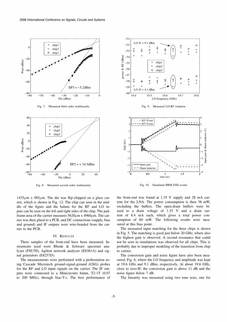
The LO to RF isolation has been measured at two different
LO amplitudes, Fig. 9. As can be seen in the figure the isolation
is at least 60 dB.
The ESD protection at the RF input has been simulated us-
ing the human body model (HBM), [6] [7]. A capaci-
tor of 100 pF is first charged and then discharged through
a 1500 Ω resistor to the test circuit. In Fig. 10 the volt-
ages at the shunt inductor and input gate of the LNA are plot-
ted for two simulated ESD events, +3 kV and -3 kV, with
a rise time of 1 ns. As can be seen in the figure, the in-
put gate of the LNA is well protected. For the negative event
the gate is also protected by a diode used to prevent an-
tenna errors during the chip fabrication, hence the lower volt-
age at the gate in Fig. 10.
V. CONCLUSION
A 20-GHz front-end in 130-nm CMOS using baluns
on glass carrier has been presented. It achieves a conver-
sion gain of 11 dB and a NF of 7 dB. The balanced topol-
ogy enables a measured third-order input referred inter-
Fig. 12. Photograph of the die mounted on carrier (5620μm x 4960μm)
cept point, IIP3, of -5.2 dBm, a second-order input referred in-
tercept, IIP2, of +34.5 dBm, and an input-referred 1 dB com-
pression point, ICP1dB , of -16 dBm. The front-end uses a dif-
ferential cross-coupling to increase the LO to RF isola-
tion and measures an isolation of 60 dB. The RF in-
put is well protected by a shunt inductor, and according to sim-
ulations it can withstand a 3 kV HBM ESD event.
VI. ACKNOWLEDGMENT
The authors would like to thank Ericsson AB in Molndal
Sweden for financing this research as part of a MEDEA+
project (2T401 HI-MISSION). They would also like to thank
Infineon Technologies for access to the state-of-the-art CMOS
technology, STMicroelectronics for access to their glass car-
rier technology, and the Knut and Alice Wallenberg foun-
dation for financial support in building up the high fre-
quency measurement laboratory.
REFERENCES
[1] B. Razavi, “A 60-GHz CMOS Receiver Front-End,” IEEE JSSC, vol. 41,no. 1, pp. 17–22, Jan. 2006.
[2] X. Guan and A. Hajimiri, “A 24GHz CMOS Front-end,” in Proc. ESS-CIRC, Sep. 2002, pp. 155–158.
[3] R. S. Engelbrecht and K. Kurokawa, “A wideband low noise L-band bal-anced transistor amplifier,” Proc. IEEE, vol. 53, no. 3, pp. 237–247, Mar.1965.
[4] N. Troedsson, http://www.indentro.com, 2008.[5] F. Stubbe, S. V. Kishore, C. Hull, and V. D. Torre, “A CMOS RF-receiver
front-end for 1 GHz applications,” in Symp. VLSI Circuits Dig. Tech.Papers, Honolulu, June 1998, pp. 80–83.
[6] STM5.1-1998, ANSI/ESD STANDARD Revised: Electrostatic DischargeSensitivity Testing - Human Body Model, http://www.esda.org, 2008.
[7] JESD22-A114A, JEDEC STANDARD Human Body Model,http://www.jedec.org, 2008.
2008 International Conference on Signals, Circuits and Systems
-4-