a 2.4 ghz 4 mw integer-n inductorless rf synthesizer · in the presence of charge pump (cp)...
TRANSCRIPT
626 IEEE JOURNAL OF SOLID-STATE CIRCUITS, VOL. 51, NO. 3, MARCH 2016
A 2.4 GHz 4 mW Integer-N Inductorless RFSynthesizer
Long Kong, Student Member, IEEE, and Behzad Razavi, Fellow, IEEE
Abstract—The high phase noise of ring oscillators has generallydiscouraged their use in RF synthesis. This paper introduces aninteger-N synthesizer that employs a type-I loop to achieve a widebandwidth, allowing the use of ring oscillators, and a master-slavesampling loop filter along with harmonic traps to suppress spurs.A 2.4 GHz prototype fabricated in 45 nm digital CMOS technologyprovides a loop bandwidth of 10 MHz and a spur level of −65 dBc.The phase noise is −114 dBc/Hz at 1 MHz offset.
Index Terms—Frequency synthesizer, harmonic trap, phase-locked loop (PLL), reference spur, voltage-controlled oscillator(VCO), Δ modulator.
I. INTRODUCTION
R F SYNTHESIS has generally shied away from ring oscil-lators due to their much more severe phase noise-power
trade-offs than those of LC topologies. Today’s multiband,multimode radios, however, require a number of synthesizersand can greatly benefit from compact, flexible implementationsafforded by ring oscillators.
This paper proposes a phase-locked loop (PLL) architecturethat can achieve a wide loop bandwidth, thus suppressing thevoltage-controlled oscillator (VCO) phase noise and allowingthe use of a ring topology. An integer-N synthesizer based onthis architecture also incorporates “harmonic traps” on the VCOcontrol line to reduce the output sidebands [1]. Most of the con-cepts introduced here are applicable to other PLL and oscillatortopologies as well. Implemented in the TSMC 45 nm digitalCMOS technology, an experimental prototype exhibits a phasenoise of −114 dBc/Hz up to 10 MHz offset with a spur levelof −65 dBc.
Section II provides the motivation for this work and reviewsthe bandwidth limitations of traditional PLLs. Section IIIdescribes the evolution of the proposed synthesizer architec-ture. Section IV deals with phase noise considerations, andSection V is concerned with spur reduction. Section VI presentsthe experimental results.
Manuscript received August 24, 2015; revised December 14, 2015; acceptedDecember 17, 2015. Date of publication February 05, 2016; date of cur-rent version March 02, 2016. This paper was approved by Associate EditorWaleed Khalil. This work was supported in part by the Qualcomm InnovationFellowship Program, in part by the Broadcom Fellowship Program, and in partby Realtek Semiconductor.
The authors are with the Department of Electrical Engineering, University ofCalifornia, Los Angeles, CA 90095-1594 USA (e-mail: [email protected]).
Color versions of one or more of the figures in this paper are available onlineat http://ieeexplore.ieee.org.
Digital Object Identifier 10.1109/JSSC.2015.2511157
II. BACKGROUND
A. General Considerations
The need for LC oscillators in RF synthesis has been solid-ified by various studies revealing that the white-noise-inducedphase noise of ring oscillators trades primarily with the powerconsumption [2], [3] and is relatively independent of the num-ber of stages. However, ring oscillators do present compellingadvantages. 1) They occupy a smaller area and can be readilyplaced within a transceiver layout with less serious concernsregarding proximity effects. 2) They entail much less couplingto and from other circuits. 3) They achieve a wider tuning rangeand can be multiplexed to cover decades of frequencies. 4) Theyreadily generate multiple phases.
That the phase noise of ring oscillators is difficult to improveat the circuit level forces us to higher levels of abstraction. Forexample, [4] processes the signals in an RF receiver (RX) so asto suppress the phase noise in reciprocal mixing. This approach,however, does not correct for the effect of phase noise on thereceived signal constellation and the error vector magnitude(EVM) (e.g., in the absence of a blocker), nor is it applicable tothe transmitter (TX). It is interesting to note that 1) applicationsentailing significant reciprocal mixing, e.g., GSM, actuallyplace tighter requirements on the TX phase noise, and 2) appli-cations specifying the phase noise by the EVM, e.g., IEEE802.11 a/b/g, impose equally stringent phase noise constraintson RX and TX. In other words, the TX phase noise is at leastas critical as the RX phase noise in most systems. It is thereforedesirable to seek a solution that can be applied to both.
B. PLL Bandwidth Limitations
Another level of abstraction at which phase noise reduc-tion can be considered is the synthesizer architecture. The loopbandwidth is generally constrained by three factors: 1) the PLLreference frequency, f REF; for example, in a mobile phone envi-ronment, only a crystal oscillator around 20 MHz is available;2) the PLL stability limit, often called “Gardner’s Limit,” andgenerally accepted to be around fREF/10 for type-II topologies;and 3) the ripple amplitude on the VCO control line and hencethe output spur level. In the presence of charge pump (CP) non-idealities, the loop bandwidth is reduced to typically fREF/20or less if spurs lower than −60 dBc are required [5]–[9].
It is helpful to briefly review the different bandwidthsencountered in PLL analysis: 1) the input–output transfer func-tion has a certain 3 dB bandwidth, which we call the “PLLbandwidth” fBW in this paper; 2) the loop transmission has
0018-9200 © 2015 IEEE. Personal use is permitted, but republication/redistribution requires IEEE permission.See http://www.ieee.org/publications_standards/publications/rights/index.html for more information.
KONG AND RAZAVI: A 2.4 GHz 4 mW INTEGER-N INDUCTORLESS RF SYNTHESIZER 627
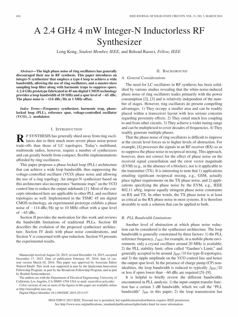
Fig. 1. (a) Traditional type-I PLL architecture. (b) Settling behavior with bandwidth of 5.6 MHz.
a unity-gain bandwidth fUGB; and 3) the VCO noise transferfunction, a high-pass response, also has a 3 dB bandwidthfn, VCO. For example, a type-II PLL with a charge pump currentIp, a loop filter capacitor C1, a VCO gain KVCO, a divide ratioN , and a unity damping factor provides 2πfBW ≈ 2.5ωn =2.5
√IpKVCO/(2π NC1), 2πfUGB ≈ 2.1ωn, and
2πfn, VCO ≈ 1.55ωn. (1)
For example, if fUGB is chosen in the range of fREF/20 tofREF/10, then
0.037fREF < fn, VCO < 0.074fREF. (2)
As mentioned above, [5]–[9] choose a loop bandwidth lessthan fREF/20, thus falling on the low side of (2).
III. PROPOSED WIDEBAND PLL
Our approach to suppressing the VCO phase noise is todevelop a PLL topology that avoids Gardner’s limit and, ifnecessary, deal with the ripple on the control voltage by addi-tional techniques. We assume fREF = 20 MHz. Let us considera type-I PLL architecture. Shown in Fig. 1(a), such a loopcontains only one integrator and can, in principle, remain sta-ble with a wide bandwidth. For example, Fig. 1(b) depictsthe circuit’s transient behavior with (R1C1)
−1= 2π(40 MHz),
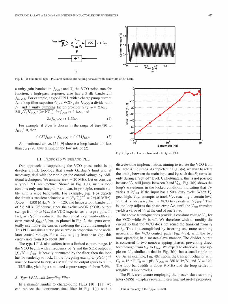
KVCO = 1500 MHz/V, N = 120, and hence a loop bandwidthof 5.6 MHz. Of course, since the exclusive-OR (XOR) outputswings from 0 to VDD, the VCO experiences a large ripple. Infact, as R1C1 is reduced, the theoretical loop bandwidth caneven exceed fREF/2, but, as plotted in Fig. 2, the spurs even-tually rise above the carrier, rendering the circuit meaningless.This PLL sustains a static phase error in proportion to the oscil-lator control voltage. For a Vcont ranging from 0 to VDD, thiserror varies from 0 to about 180◦.
The type-I PLL also suffers from a limited capture range. Ifthe VCO begins with a frequency of f1 and the XOR output at|f1/N − fREF| is heavily attenuated by the filter, then the loophas no tendency to lock. In the foregoing example, (R1C1)
−1
must be lowered to 2π(0.47 MHz) for the output spurs to fall to−35.5 dBc, yielding a simulated capture range of about 7.4%.
A. Type-I PLL with Sampling Filter
In a manner similar to charge-pump PLLs [10], [11], wecan replace the continuous-time filter in Fig. 1(a) with a
Fig. 2. Spur level versus bandwidth for type-I PLL.
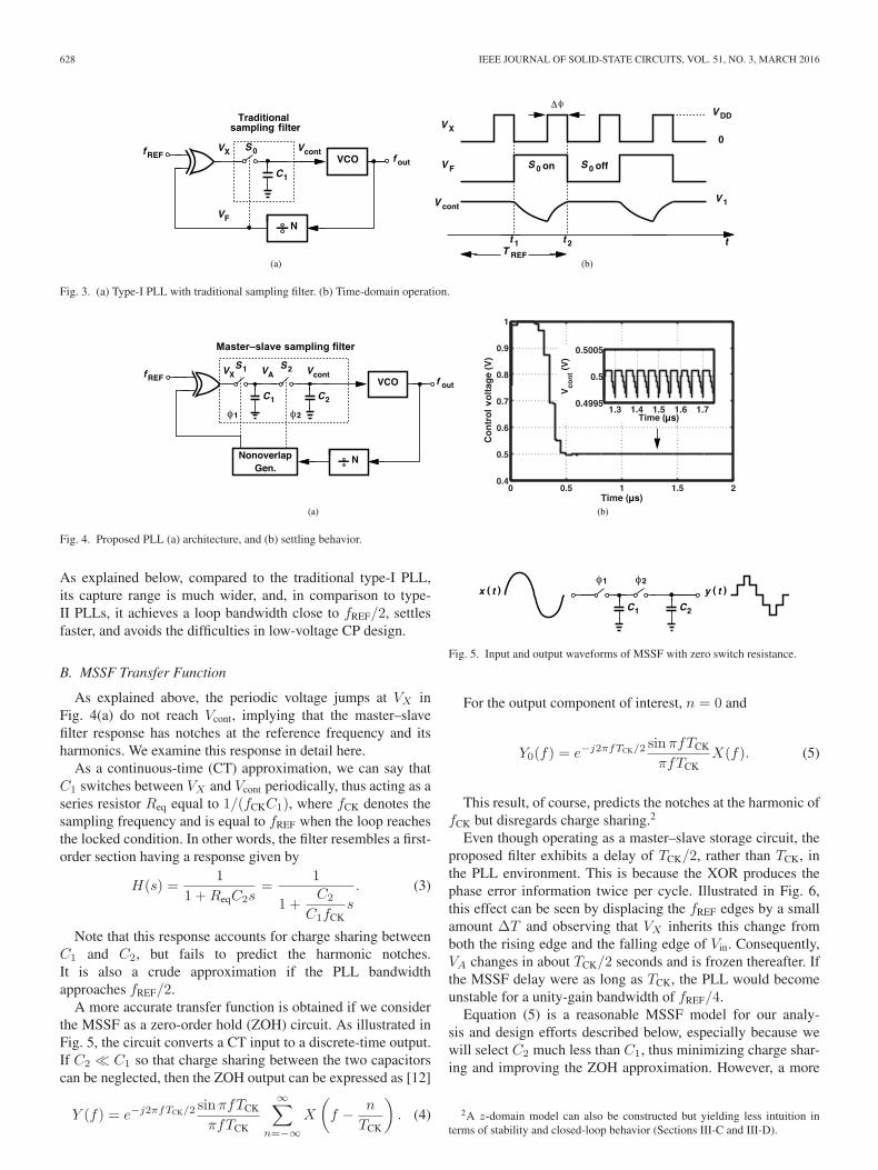
discrete-time implementation, aiming to isolate the VCO fromthe large XOR jumps. As depicted in Fig. 3(a), we wish to selectthe timing between the main input and VF such that S0 turns ON
only during a “settled” level. Unfortunately, this is not possiblebecause VX still jumps between 0 and VDD. Fig. 3(b) shows theloop’s waveforms in the locked condition, indicating that VX
varies at 2fREF if the input has a 50% duty cycle. When VF
goes high, Vcont attempts to track VX , reaching a certain levelV1 that is necessary for the VCO to operate at NfREF.1 Thatis, the loop adjusts the phase error Δφ, until the Vcont transientyields a value of V1 at the end of one TREF.
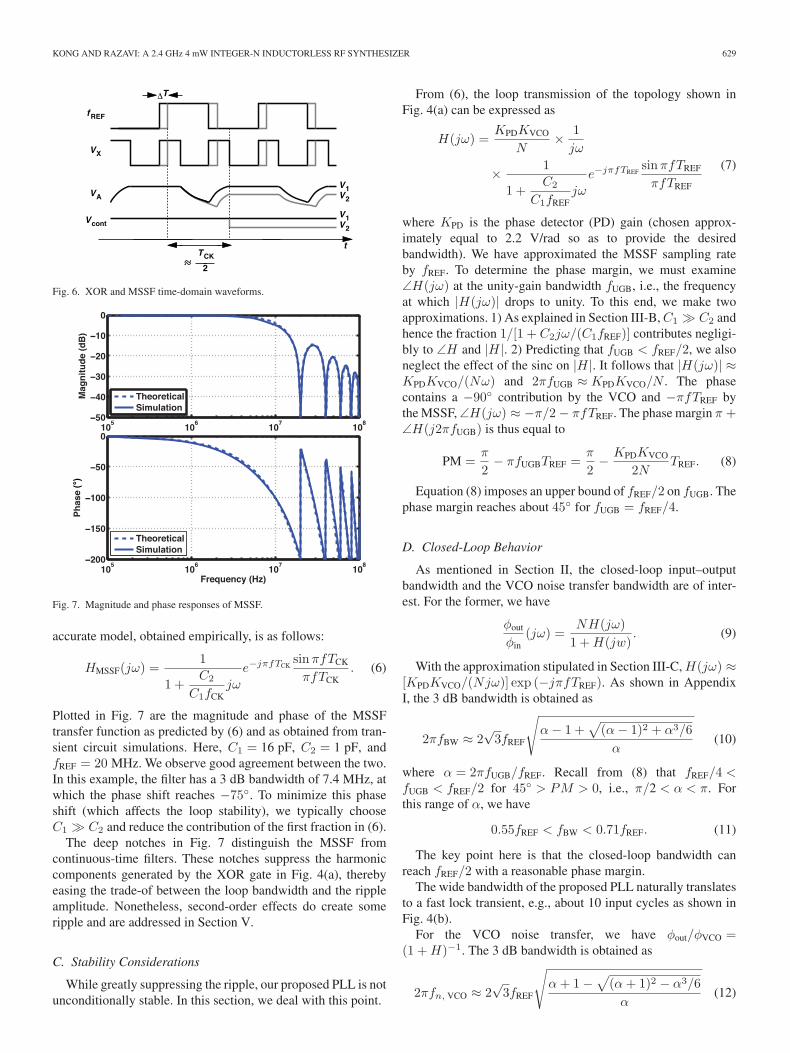
The above technique does provide a constant voltage V1, forthe VCO while S0 is off. We therefore wish to modify thecircuit so that the VCO does not sense the transient from t1to t2. This is accomplished by inserting one more samplingnetwork in the VCO control path [Fig. 4(a)], with the twonow operating in a master–slave manner. The divider outputis converted to two nonoverlapping phases, preventing directfeedthrough from VX to Vcont. We expect to observe a large rip-ple on C1, similar to that in Fig. 3(b), but a small ripple onC2. As an example, Fig. 4(b) shows the transient behavior withC1 = 16 pF, C2 = 1 pF, KVCO = 280 MHz/V, and N = 120.The loop bandwidth is about 9 MHz and the loop settles inroughly 10 input cycles.
The PLL architecture employing the master–slave samplingfilter (MSSF) displays several interesting and useful properties.
1This is true only if the ripple is small.
628 IEEE JOURNAL OF SOLID-STATE CIRCUITS, VOL. 51, NO. 3, MARCH 2016
Fig. 3. (a) Type-I PLL with traditional sampling filter. (b) Time-domain operation.
Fig. 4. Proposed PLL (a) architecture, and (b) settling behavior.
As explained below, compared to the traditional type-I PLL,its capture range is much wider, and, in comparison to type-II PLLs, it achieves a loop bandwidth close to fREF/2, settlesfaster, and avoids the difficulties in low-voltage CP design.
B. MSSF Transfer Function
As explained above, the periodic voltage jumps at VX inFig. 4(a) do not reach Vcont, implying that the master–slavefilter response has notches at the reference frequency and itsharmonics. We examine this response in detail here.
As a continuous-time (CT) approximation, we can say thatC1 switches between VX and Vcont periodically, thus acting as aseries resistor Req equal to 1/(fCKC1), where fCK denotes thesampling frequency and is equal to fREF when the loop reachesthe locked condition. In other words, the filter resembles a first-order section having a response given by
H(s) =1
1 +ReqC2s=
1
1 +C2
C1fCKs. (3)
Note that this response accounts for charge sharing betweenC1 and C2, but fails to predict the harmonic notches.It is also a crude approximation if the PLL bandwidthapproaches fREF/2.
A more accurate transfer function is obtained if we considerthe MSSF as a zero-order hold (ZOH) circuit. As illustrated inFig. 5, the circuit converts a CT input to a discrete-time output.If C2 � C1 so that charge sharing between the two capacitorscan be neglected, then the ZOH output can be expressed as [12]
Y (f) = e−j2πfTCK/2sinπfTCK
πfTCK
∞∑n=−∞
X
(f − n
TCK
). (4)
Fig. 5. Input and output waveforms of MSSF with zero switch resistance.
For the output component of interest, n = 0 and
Y0(f) = e−j2πfTCK/2sinπfTCK
πfTCKX(f). (5)
This result, of course, predicts the notches at the harmonic offCK but disregards charge sharing.2
Even though operating as a master–slave storage circuit, theproposed filter exhibits a delay of TCK/2, rather than TCK, inthe PLL environment. This is because the XOR produces thephase error information twice per cycle. Illustrated in Fig. 6,this effect can be seen by displacing the fREF edges by a smallamount ΔT and observing that VX inherits this change fromboth the rising edge and the falling edge of Vin. Consequently,VA changes in about TCK/2 seconds and is frozen thereafter. Ifthe MSSF delay were as long as TCK, the PLL would becomeunstable for a unity-gain bandwidth of fREF/4.
Equation (5) is a reasonable MSSF model for our analy-sis and design efforts described below, especially because wewill select C2 much less than C1, thus minimizing charge shar-ing and improving the ZOH approximation. However, a more
2A z-domain model can also be constructed but yielding less intuition interms of stability and closed-loop behavior (Sections III-C and III-D).
KONG AND RAZAVI: A 2.4 GHz 4 mW INTEGER-N INDUCTORLESS RF SYNTHESIZER 629
Fig. 6. XOR and MSSF time-domain waveforms.
Fig. 7. Magnitude and phase responses of MSSF.
accurate model, obtained empirically, is as follows:
HMSSF(jω) =1
1 +C2
C1fCKjω
e−jπfTCKsinπfTCK
πfTCK. (6)
Plotted in Fig. 7 are the magnitude and phase of the MSSFtransfer function as predicted by (6) and as obtained from tran-sient circuit simulations. Here, C1 = 16 pF, C2 = 1 pF, andfREF = 20 MHz. We observe good agreement between the two.In this example, the filter has a 3 dB bandwidth of 7.4 MHz, atwhich the phase shift reaches −75◦. To minimize this phaseshift (which affects the loop stability), we typically chooseC1 � C2 and reduce the contribution of the first fraction in (6).
The deep notches in Fig. 7 distinguish the MSSF fromcontinuous-time filters. These notches suppress the harmoniccomponents generated by the XOR gate in Fig. 4(a), therebyeasing the trade-of between the loop bandwidth and the rippleamplitude. Nonetheless, second-order effects do create someripple and are addressed in Section V.
C. Stability Considerations
While greatly suppressing the ripple, our proposed PLL is notunconditionally stable. In this section, we deal with this point.
From (6), the loop transmission of the topology shown inFig. 4(a) can be expressed as
H(jω) =KPDKVCO
N× 1
jω
× 1
1 +C2
C1fREFjω
e−jπfTREFsinπfTREF
πfTREF
(7)
where KPD is the phase detector (PD) gain (chosen approx-imately equal to 2.2 V/rad so as to provide the desiredbandwidth). We have approximated the MSSF sampling rateby fREF. To determine the phase margin, we must examine∠H(jω) at the unity-gain bandwidth fUGB, i.e., the frequencyat which |H(jω)| drops to unity. To this end, we make twoapproximations. 1) As explained in Section III-B, C1 � C2 andhence the fraction 1/[1 + C2jω/(C1fREF)] contributes negligi-bly to ∠H and |H|. 2) Predicting that fUGB < fREF/2, we alsoneglect the effect of the sinc on |H|. It follows that |H(jω)| ≈KPDKVCO/(Nω) and 2πfUGB ≈ KPDKVCO/N . The phasecontains a −90◦ contribution by the VCO and −πfTREF bythe MSSF, ∠H(jω) ≈ −π/2− πfTREF. The phase margin π +∠H(j2πfUGB) is thus equal to
PM =π
2− πfUGBTREF =
π
2− KPDKVCO
2NTREF. (8)
Equation (8) imposes an upper bound of fREF/2 on fUGB. Thephase margin reaches about 45◦ for fUGB = fREF/4.
D. Closed-Loop Behavior
As mentioned in Section II, the closed-loop input–outputbandwidth and the VCO noise transfer bandwidth are of inter-est. For the former, we have
φout
φin(jω) =
NH(jω)
1 +H(jw). (9)
With the approximation stipulated in Section III-C, H(jω) ≈[KPDKVCO/(Njω)] exp (−jπfTREF). As shown in AppendixI, the 3 dB bandwidth is obtained as
2πfBW ≈ 2√3fREF
√α− 1 +
√(α− 1)2 + α3/6
α(10)
where α = 2πfUGB/fREF. Recall from (8) that fREF/4 <fUGB < fREF/2 for 45◦ > PM > 0, i.e., π/2 < α < π. Forthis range of α, we have
0.55fREF < fBW < 0.71fREF. (11)
The key point here is that the closed-loop bandwidth canreach fREF/2 with a reasonable phase margin.
The wide bandwidth of the proposed PLL naturally translatesto a fast lock transient, e.g., about 10 input cycles as shown inFig. 4(b).
For the VCO noise transfer, we have φout/φVCO =(1 +H)−1. The 3 dB bandwidth is obtained as
2πfn, VCO ≈ 2√3fREF
√α+ 1−√
(α+ 1)2 − α3/6
α(12)
630 IEEE JOURNAL OF SOLID-STATE CIRCUITS, VOL. 51, NO. 3, MARCH 2016
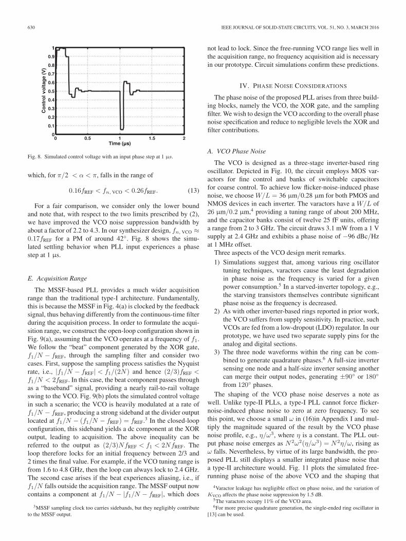
Fig. 8. Simulated control voltage with an input phase step at 1 µs.
which, for π/2 < α < π, falls in the range of
0.16fREF < fn, VCO < 0.26fREF. (13)
For a fair comparison, we consider only the lower boundand note that, with respect to the two limits prescribed by (2),we have improved the VCO noise suppression bandwidth byabout a factor of 2.2 to 4.3. In our synthesizer design, fn, VCO ≈0.17fREF for a PM of around 42◦. Fig. 8 shows the simu-lated settling behavior when PLL input experiences a phasestep at 1 µs.
E. Acquisition Range
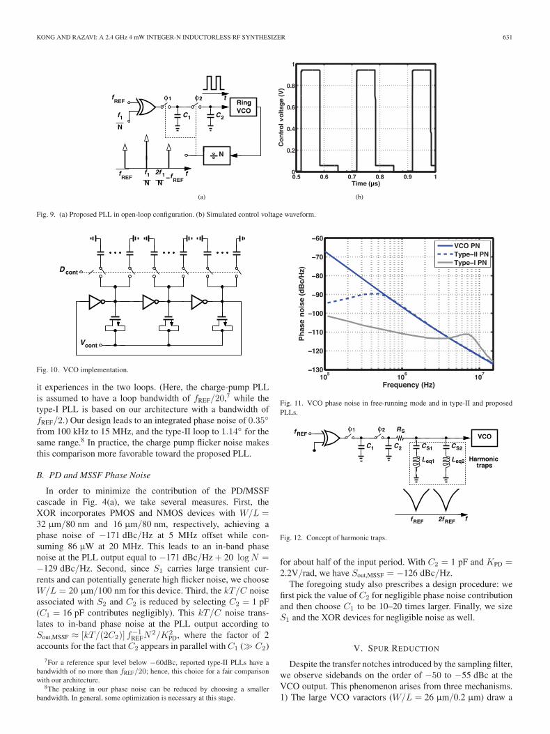
The MSSF-based PLL provides a much wider acquisitionrange than the traditional type-I architecture. Fundamentally,this is because the MSSF in Fig. 4(a) is clocked by the feedbacksignal, thus behaving differently from the continuous-time filterduring the acquisition process. In order to formulate the acqui-sition range, we construct the open-loop configuration shown inFig. 9(a), assuming that the VCO operates at a frequency of f1.We follow the “beat” component generated by the XOR gate,f1/N − fREF, through the sampling filter and consider twocases. First, suppose the sampling process satisfies the Nyquistrate, i.e., |f1/N − fREF| < f1/(2N) and hence (2/3)fREF <f1/N < 2fREF. In this case, the beat component passes throughas a “baseband” signal, providing a nearly rail-to-rail voltageswing to the VCO. Fig. 9(b) plots the simulated control voltagein such a scenario; the VCO is heavily modulated at a rate off1/N − fREF, producing a strong sideband at the divider outputlocated at f1/N − (f1/N − fREF) = fREF.3 In the closed-loopconfiguration, this sideband yields a dc component at the XORoutput, leading to acquisition. The above inequality can bereferred to the output as (2/3)NfREF < f1 < 2NfREF. Theloop therefore locks for an initial frequency between 2/3 and2 times the final value. For example, if the VCO tuning range isfrom 1.6 to 4.8 GHz, then the loop can always lock to 2.4 GHz.The second case arises if the beat experiences aliasing, i.e., iff1/N falls outside the acquisition range. The MSSF output nowcontains a component at f1/N − |f1/N − fREF|, which does
3MSSF sampling clock too carries sidebands, but they negligibly contributeto the MSSF output.
not lead to lock. Since the free-running VCO range lies well inthe acquisition range, no frequency acquisition aid is necessaryin our prototype. Circuit simulations confirm these predictions.
IV. PHASE NOISE CONSIDERATIONS
The phase noise of the proposed PLL arises from three build-ing blocks, namely the VCO, the XOR gate, and the samplingfilter. We wish to design the VCO according to the overall phasenoise specification and reduce to negligible levels the XOR andfilter contributions.
A. VCO Phase Noise
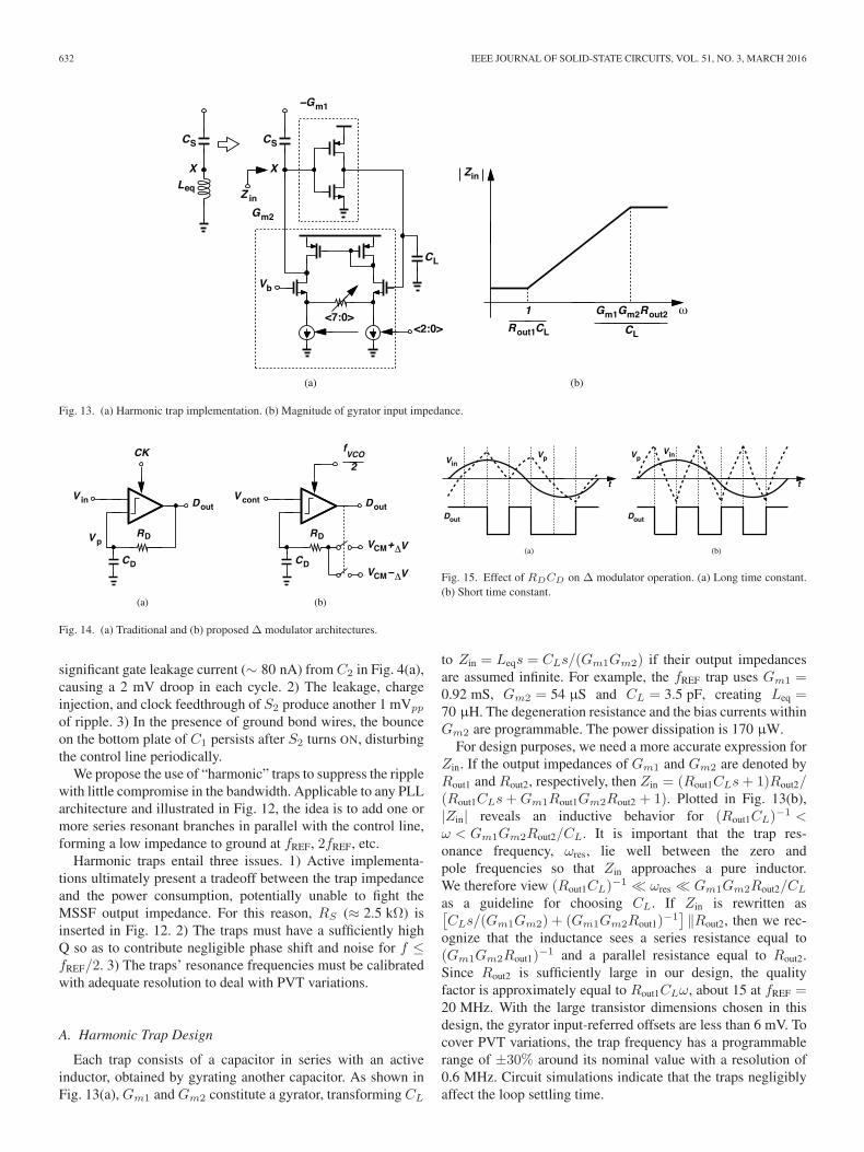
The VCO is designed as a three-stage inverter-based ringoscillator. Depicted in Fig. 10, the circuit employs MOS var-actors for fine control and banks of switchable capacitorsfor coarse control. To achieve low flicker-noise-induced phasenoise, we choose W/L = 36 µm/0.28 µm for both PMOS andNMOS devices in each inverter. The varactors have a W/L of26 µm/0.2 µm,4 providing a tuning range of about 200 MHz,and the capacitor banks consist of twelve 25 fF units, offeringa range from 2 to 3 GHz. The circuit draws 3.1 mW from a 1 Vsupply at 2.4 GHz and exhibits a phase noise of −96 dBc/Hzat 1 MHz offset.
Three aspects of the VCO design merit remarks.
1) Simulations suggest that, among various ring oscillatortuning techniques, varactors cause the least degradationin phase noise as the frequency is varied for a givenpower consumption.5 In a starved-inverter topology, e.g.,the starving transistors themselves contribute significantphase noise as the frequency is decreased.
2) As with other inverter-based rings reported in prior work,the VCO suffers from supply sensitivity. In practice, suchVCOs are fed from a low-dropout (LDO) regulator. In ourprototype, we have used two separate supply pins for theanalog and digital sections.
3) The three node waveforms within the ring can be com-bined to generate quadrature phases.6 A full-size invertersensing one node and a half-size inverter sensing anothercan merge their output nodes, generating ±90◦ or 180◦
from 120◦ phases.
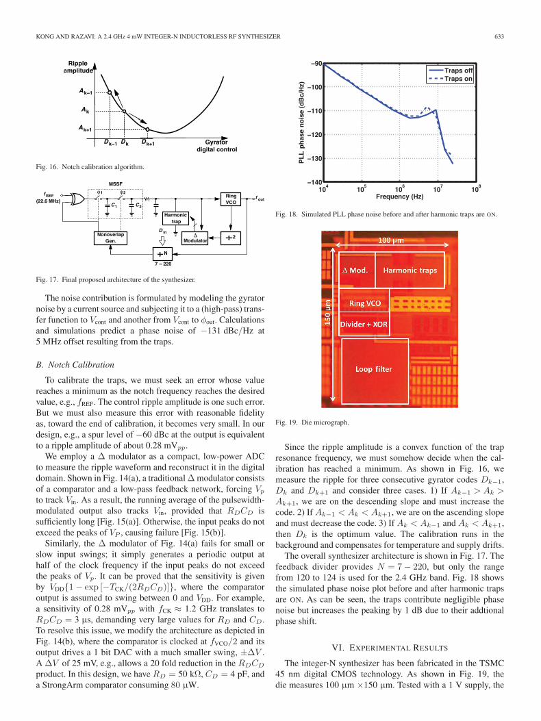
The shaping of the VCO phase noise deserves a note aswell. Unlike type-II PLLs, a type-I PLL cannot force flicker-noise-induced phase noise to zero at zero frequency. To seethis point, we choose a small ω in (16)in Appendix I and mul-tiply the magnitude squared of the result by the VCO phasenoise profile, e.g., η/ω3, where η is a constant. The PLL out-put phase noise emerges as N2ω2(η/ω3) = N2η/ω, rising asω falls. Nevertheless, by virtue of its large bandwidth, the pro-posed PLL still displays a smaller integrated phase noise thata type-II architecture would. Fig. 11 plots the simulated free-running phase noise of the above VCO and the shaping that
4Varactor leakage has negligible effect on phase noise, and the variation ofKVCO affects the phase noise suppression by 1.5 dB.
5The varactors occupy 11% of the VCO area.6For more precise quadrature generation, the single-ended ring oscillator in
[13] can be used.
KONG AND RAZAVI: A 2.4 GHz 4 mW INTEGER-N INDUCTORLESS RF SYNTHESIZER 631
Fig. 9. (a) Proposed PLL in open-loop configuration. (b) Simulated control voltage waveform.
Fig. 10. VCO implementation.
it experiences in the two loops. (Here, the charge-pump PLLis assumed to have a loop bandwidth of fREF/20,7 while thetype-I PLL is based on our architecture with a bandwidth offREF/2.) Our design leads to an integrated phase noise of 0.35◦
from 100 kHz to 15 MHz, and the type-II loop to 1.14◦ for thesame range.8 In practice, the charge pump flicker noise makesthis comparison more favorable toward the proposed PLL.
B. PD and MSSF Phase Noise
In order to minimize the contribution of the PD/MSSFcascade in Fig. 4(a), we take several measures. First, theXOR incorporates PMOS and NMOS devices with W/L =32 µm/80 nm and 16 µm/80 nm, respectively, achieving aphase noise of −171 dBc/Hz at 5 MHz offset while con-suming 86 µW at 20 MHz. This leads to an in-band phasenoise at the PLL output equal to −171 dBc/Hz + 20 logN =−129 dBc/Hz. Second, since S1 carries large transient cur-rents and can potentially generate high flicker noise, we chooseW/L = 20 µm/100 nm for this device. Third, the kT/C noiseassociated with S2 and C2 is reduced by selecting C2 = 1 pF(C1 = 16 pF contributes negligibly). This kT/C noise trans-lates to in-band phase noise at the PLL output according toSout,MSSF ≈ [kT/(2C2)] f
−1REFN
2/K2PD, where the factor of 2
accounts for the fact that C2 appears in parallel with C1 (� C2)
7For a reference spur level below −60dBc, reported type-II PLLs have abandwidth of no more than fREF/20; hence, this choice for a fair comparisonwith our architecture.
8The peaking in our phase noise can be reduced by choosing a smallerbandwidth. In general, some optimization is necessary at this stage.
Fig. 11. VCO phase noise in free-running mode and in type-II and proposedPLLs.
Fig. 12. Concept of harmonic traps.
for about half of the input period. With C2 = 1 pF and KPD =2.2V/rad, we have Sout,MSSF = −126 dBc/Hz.
The foregoing study also prescribes a design procedure: wefirst pick the value of C2 for negligible phase noise contributionand then choose C1 to be 10–20 times larger. Finally, we sizeS1 and the XOR devices for negligible noise as well.
V. SPUR REDUCTION
Despite the transfer notches introduced by the sampling filter,we observe sidebands on the order of −50 to −55 dBc at theVCO output. This phenomenon arises from three mechanisms.1) The large VCO varactors (W/L = 26 µm/0.2 µm) draw a
632 IEEE JOURNAL OF SOLID-STATE CIRCUITS, VOL. 51, NO. 3, MARCH 2016
Fig. 13. (a) Harmonic trap implementation. (b) Magnitude of gyrator input impedance.
Fig. 14. (a) Traditional and (b) proposed Δ modulator architectures.
significant gate leakage current (∼ 80 nA) from C2 in Fig. 4(a),causing a 2 mV droop in each cycle. 2) The leakage, chargeinjection, and clock feedthrough of S2 produce another 1 mVpp
of ripple. 3) In the presence of ground bond wires, the bounceon the bottom plate of C1 persists after S2 turns ON, disturbingthe control line periodically.
We propose the use of “harmonic” traps to suppress the ripplewith little compromise in the bandwidth. Applicable to any PLLarchitecture and illustrated in Fig. 12, the idea is to add one ormore series resonant branches in parallel with the control line,forming a low impedance to ground at fREF, 2fREF, etc.
Harmonic traps entail three issues. 1) Active implementa-tions ultimately present a tradeoff between the trap impedanceand the power consumption, potentially unable to fight theMSSF output impedance. For this reason, RS (≈ 2.5 kΩ) isinserted in Fig. 12. 2) The traps must have a sufficiently highQ so as to contribute negligible phase shift and noise for f ≤fREF/2. 3) The traps’ resonance frequencies must be calibratedwith adequate resolution to deal with PVT variations.
A. Harmonic Trap Design
Each trap consists of a capacitor in series with an activeinductor, obtained by gyrating another capacitor. As shown inFig. 13(a), Gm1 and Gm2 constitute a gyrator, transforming CL
Fig. 15. Effect of RDCD on Δ modulator operation. (a) Long time constant.(b) Short time constant.
to Zin = Leqs = CLs/(Gm1Gm2) if their output impedancesare assumed infinite. For example, the fREF trap uses Gm1 =0.92 mS, Gm2 = 54 µS and CL = 3.5 pF, creating Leq =70 µH. The degeneration resistance and the bias currents withinGm2 are programmable. The power dissipation is 170 µW.
For design purposes, we need a more accurate expression forZin. If the output impedances of Gm1 and Gm2 are denoted byRout1 and Rout2, respectively, then Zin = (Rout1CLs+ 1)Rout2/(Rout1CLs+Gm1Rout1Gm2Rout2 + 1). Plotted in Fig. 13(b),|Zin| reveals an inductive behavior for (Rout1CL)
−1 <ω < Gm1Gm2Rout2/CL. It is important that the trap res-onance frequency, ωres, lie well between the zero andpole frequencies so that Zin approaches a pure inductor.We therefore view (Rout1CL)
−1 � ωres � Gm1Gm2Rout2/CL
as a guideline for choosing CL. If Zin is rewritten as[CLs/(Gm1Gm2) + (Gm1Gm2Rout1)
−1] ‖Rout2, then we rec-
ognize that the inductance sees a series resistance equal to(Gm1Gm2Rout1)
−1 and a parallel resistance equal to Rout2.Since Rout2 is sufficiently large in our design, the qualityfactor is approximately equal to Rout1CLω, about 15 at fREF =20 MHz. With the large transistor dimensions chosen in thisdesign, the gyrator input-referred offsets are less than 6 mV. Tocover PVT variations, the trap frequency has a programmablerange of ±30% around its nominal value with a resolution of0.6 MHz. Circuit simulations indicate that the traps negligiblyaffect the loop settling time.
KONG AND RAZAVI: A 2.4 GHz 4 mW INTEGER-N INDUCTORLESS RF SYNTHESIZER 633
Fig. 16. Notch calibration algorithm.
Fig. 17. Final proposed architecture of the synthesizer.
The noise contribution is formulated by modeling the gyratornoise by a current source and subjecting it to a (high-pass) trans-fer function to Vcont and another from Vcont to φout. Calculationsand simulations predict a phase noise of −131 dBc/Hz at5 MHz offset resulting from the traps.
B. Notch Calibration
To calibrate the traps, we must seek an error whose valuereaches a minimum as the notch frequency reaches the desiredvalue, e.g., fREF. The control ripple amplitude is one such error.But we must also measure this error with reasonable fidelityas, toward the end of calibration, it becomes very small. In ourdesign, e.g., a spur level of −60 dBc at the output is equivalentto a ripple amplitude of about 0.28 mVpp.
We employ a Δ modulator as a compact, low-power ADCto measure the ripple waveform and reconstruct it in the digitaldomain. Shown in Fig. 14(a), a traditional Δ modulator consistsof a comparator and a low-pass feedback network, forcing Vp
to track Vin. As a result, the running average of the pulsewidth-modulated output also tracks Vin, provided that RDCD issufficiently long [Fig. 15(a)]. Otherwise, the input peaks do notexceed the peaks of VP , causing failure [Fig. 15(b)].
Similarly, the Δ modulator of Fig. 14(a) fails for small orslow input swings; it simply generates a periodic output athalf of the clock frequency if the input peaks do not exceedthe peaks of Vp. It can be proved that the sensitivity is givenby VDD{1− exp [−TCK/(2RDCD)]}, where the comparatoroutput is assumed to swing between 0 and VDD. For example,a sensitivity of 0.28 mVpp with fCK ≈ 1.2 GHz translates toRDCD = 3 µs, demanding very large values for RD and CD.To resolve this issue, we modify the architecture as depicted inFig. 14(b), where the comparator is clocked at fVCO/2 and itsoutput drives a 1 bit DAC with a much smaller swing, ±ΔV .A ΔV of 25 mV, e.g., allows a 20 fold reduction in the RDCD
product. In this design, we have RD = 50 kΩ, CD = 4 pF, anda StrongArm comparator consuming 80 µW.
Fig. 18. Simulated PLL phase noise before and after harmonic traps are ON.
Fig. 19. Die micrograph.
Since the ripple amplitude is a convex function of the trapresonance frequency, we must somehow decide when the cal-ibration has reached a minimum. As shown in Fig. 16, wemeasure the ripple for three consecutive gyrator codes Dk−1,Dk and Dk+1 and consider three cases. 1) If Ak−1 > Ak >Ak+1, we are on the descending slope and must increase thecode. 2) If Ak−1 < Ak < Ak+1, we are on the ascending slopeand must decrease the code. 3) If Ak < Ak−1 and Ak < Ak+1,then Dk is the optimum value. The calibration runs in thebackground and compensates for temperature and supply drifts.
The overall synthesizer architecture is shown in Fig. 17. Thefeedback divider provides N = 7− 220, but only the rangefrom 120 to 124 is used for the 2.4 GHz band. Fig. 18 showsthe simulated phase noise plot before and after harmonic trapsare ON. As can be seen, the traps contribute negligible phasenoise but increases the peaking by 1 dB due to their addtionalphase shift.
VI. EXPERIMENTAL RESULTS
The integer-N synthesizer has been fabricated in the TSMC45 nm digital CMOS technology. As shown in Fig. 19, thedie measures 100 µm ×150 µm. Tested with a 1 V supply, the
634 IEEE JOURNAL OF SOLID-STATE CIRCUITS, VOL. 51, NO. 3, MARCH 2016
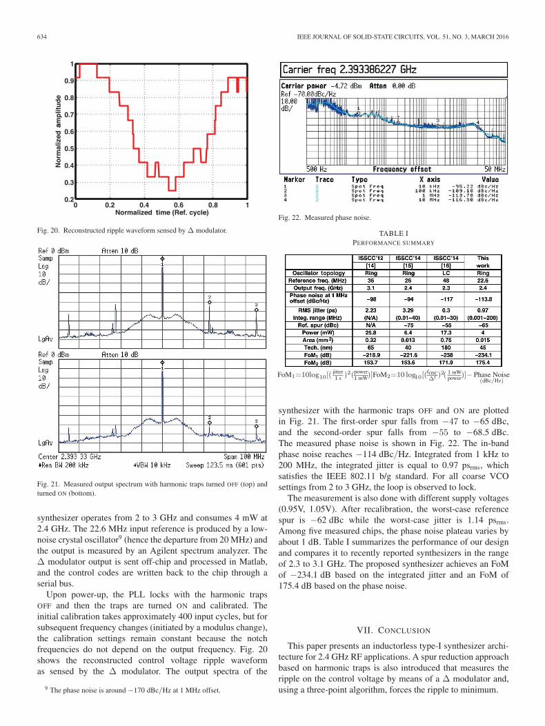
Fig. 20. Reconstructed ripple waveform sensed by Δ modulator.
Fig. 21. Measured output spectrum with harmonic traps turned OFF (top) andturned ON (bottom).
synthesizer operates from 2 to 3 GHz and consumes 4 mW at2.4 GHz. The 22.6 MHz input reference is produced by a low-noise crystal oscillator9 (hence the departure from 20 MHz) andthe output is measured by an Agilent spectrum analyzer. TheΔ modulator output is sent off-chip and processed in Matlab,and the control codes are written back to the chip through aserial bus.
Upon power-up, the PLL locks with the harmonic trapsOFF and then the traps are turned ON and calibrated. Theinitial calibration takes approximately 400 input cycles, but forsubsequent frequency changes (initiated by a modulus change),the calibration settings remain constant because the notchfrequencies do not depend on the output frequency. Fig. 20shows the reconstructed control voltage ripple waveformas sensed by the Δ modulator. The output spectra of the
9 The phase noise is around −170 dBc/Hz at 1 MHz offset.
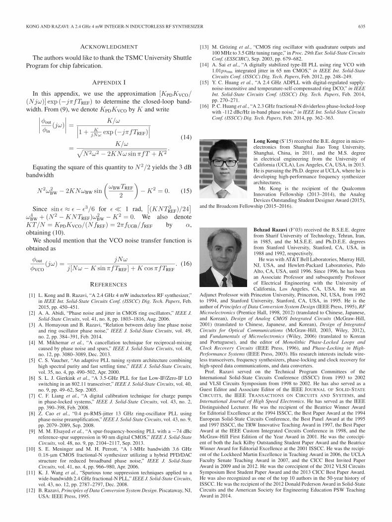
Fig. 22. Measured phase noise.
TABLE IPERFORMANCE SUMMARY
FoM1=10log10[(jitter1 s )2(power
1 mW)]FoM2=10 log10[(fOSCΔf )
2( 1 mWpower)]− Phase Noise
(dBc/Hz)
synthesizer with the harmonic traps OFF and ON are plottedin Fig. 21. The first-order spur falls from −47 to −65 dBc,and the second-order spur falls from −55 to −68.5 dBc.The measured phase noise is shown in Fig. 22. The in-bandphase noise reaches −114 dBc/Hz. Integrated from 1 kHz to200 MHz, the integrated jitter is equal to 0.97 psrms, whichsatisfies the IEEE 802.11 b/g standard. For all coarse VCOsettings from 2 to 3 GHz, the loop is observed to lock.
The measurement is also done with different supply voltages(0.95V, 1.05V). After recalibration, the worst-case referencespur is −62 dBc while the worst-case jitter is 1.14 psrms.Among five measured chips, the phase noise plateau varies byabout 1 dB. Table I summarizes the performance of our designand compares it to recently reported synthesizers in the rangeof 2.3 to 3.1 GHz. The proposed synthesizer achieves an FoMof −234.1 dB based on the integrated jitter and an FoM of175.4 dB based on the phase noise.
VII. CONCLUSION
This paper presents an inductorless type-I synthesizer archi-tecture for 2.4 GHz RF applications. A spur reduction approachbased on harmonic traps is also introduced that measures theripple on the control voltage by means of a Δ modulator and,using a three-point algorithm, forces the ripple to minimum.
KONG AND RAZAVI: A 2.4 GHz 4 mW INTEGER-N INDUCTORLESS RF SYNTHESIZER 635
ACKNOWLEDGMENT
The authors would like to thank the TSMC University ShuttleProgram for chip fabrication.
APPENDIX I
In this appendix, we use the approximation [KPDKVCO/(Njω)] exp (−jπfTREF) to determine the closed-loop band-width. From (9), we denote KPDKVCO by K and write∣∣∣∣φout
φin(jω)
∣∣∣∣ = K/ω∣∣∣1 + KjNω exp (−jπfTREF)
∣∣∣=
K/ω√N2ω2 − 2KNω sinπfT +K2
.
(14)
Equating the square of this quantity to N2/2 yields the 3 dBbandwidth
N2ω2BW − 2KNωBW sin
(ωBWTREF
2
)−K2 = 0. (15)
Since sin ε ≈ ε− ε3/6 for ε � 1 rad,[(KNT 3
REF)/24]
ω4BW + (N2 −KNTREF)ω
2BW −K2 = 0. We also denote
KT/N = KPDKVCO/(NfREF) = 2πfUGB/fREF by α,obtaining (10).
We should mention that the VCO noise transfer function isobtained as
φout
φVCO(jω) =
jNω
j[Nω −K sinπfTREF] +K cosπfTREF. (16)
REFERENCES
[1] L. Kong and B. Razavi, “A 2.4 GHz 4 mW inductorless RF synthesizer,”in IEEE Int. Solid-State Circuits Conf. (ISSCC) Dig. Tech. Papers, Feb.2015, pp. 450–451.
[2] A. A. Abidi, “Phase noise and jitter in CMOS ring oscillators,” IEEE J.Solid-State Circuits, vol. 41, no. 8, pp. 1803–1816, Aug. 2006.
[3] A. Homayoun and B. Razavi, “Relation between delay line phase noiseand ring oscillator phase noise,” IEEE J. Solid-State Circuits, vol. 49,no. 2, pp. 384–391, Feb. 2014.
[4] M. Mikhemar et al., “A cancellation technique for reciprocal-mixingcaused by phase noise and spurs,” IEEE J. Solid-State Circuits, vol. 48,no. 12, pp. 3080–3089, Dec. 2013.
[5] C. S. Vaucher, “An adaptive PLL tuning system architecture combininghigh spectral purity and fast settling time,” IEEE J. Solid-State Circuits,vol. 35, no. 4, pp. 490–502, Apr. 2000.
[6] S. L. J. Gierkink et al., “A 3.5-GHz PLL for fast Low-IF/Zero-IF LOswitching in an 802.11 transceiver,” IEEE J. Solid-State Circuits, vol. 40,no. 9, pp. 49–62, Sep. 2005.
[7] C. F. Liang et al., “A digital calibration technique for charge pumpsin phase-locked systems,” IEEE J. Solid-State Circuits, vol. 43, no. 2,pp. 390–398, Feb. 2008.
[8] Z. Cao et al., “0.4 ps-RMS-jitter 13 GHz ring-oscillator PLL usingphase-noise preamplification,” IEEE J. Solid-State Circuits, vol. 43, no. 9,pp. 2079–2089, Sep. 2008.
[9] M. M. Elsayed et al., “A spur-frequency-boosting PLL with a −74 dBcreference-spur suppression in 90 nm digital CMOS,” IEEE J. Solid-StateCircuits, vol. 48, no. 9, pp. 2104–2117, Sep. 2013.
[10] S. E. Meninger and M. H. Perrott, “A 1-MHz bandwidth 3.6 GHz0.18-µm CMOS fractional-N synthesizer utilizing a hybrid PFD/DACstructure for reduced broadband phase noise,” IEEE J. Solid-StateCircuits, vol. 41, no. 4, pp. 966–980, Apr. 2006.
[11] K. J. Wang et al., “Spurious tone suppression techniques applied to awide-bandwidth 2.4 GHz fractional-N PLL,” IEEE J. Solid-State Circuits,vol. 43, no. 12, pp. 2787–2797, Dec. 2008.
[12] B. Razavi, Principles of Data Conversion System Design. Piscataway, NJ,USA: IEEE Press, 1995.
[13] M. Grözing et al., “CMOS ring oscillator with quadrature outputs and100 MHz to 3.5 GHz tuning range,” in Proc. 29th Eur. Solid-State CircuitsConf. (ESSCIRC), Sep. 2003, pp. 679–682.
[14] A. Sai et al., “A digitally stabilized type-III PLL using ring VCO with1.01psrms integrated jitter in 65 nm CMOS,” in IEEE Int. Solid-StateCircuits Conf. (ISSCC) Dig. Tech. Papers, Feb. 2012, pp. 248–249.
[15] Y. C. Huang et al., “A 2.4 GHz ADPLL with digital-regulated supply-noise-insensitive and temperature-self-compensated ring DCO,” in IEEEInt. Solid-State Circuits Conf. (ISSCC) Dig. Tech. Papers, Feb. 2014,pp. 270–271.
[16] P. C. Huang et al., “A 2.3 GHz fractional-N dividerless phase-locked-loopwith -112 dBc/Hz in-band phase noise,” in IEEE Int. Solid-State CircuitsConf. (ISSCC) Dig. Tech. Papers, Feb. 2014, pp. 362–363.
Long Kong (S’15) received the B.E. degree in micro-electronics from Shanghai Jiao Tong University,Shanghai, China, in 2011, and the M.S. degreein electrical engineering from the University ofCalifornia (UCLA), Los Angeles, CA, USA, in 2013.He is pursuing the Ph.D. degree at UCLA, where he isdeveloping high-performance frequency synthesizerarchitectures.
Mr. Kong is the recipient of the QualcommInnovation Fellowship (2013–2014), the AnalogDevices Outstanding Student Designer Award (2015),
and the Broadcom Fellowship (2015–2016).
Behzad Razavi (F’03) received the B.S.E.E. degreefrom Sharif University of Technology, Tehran, Iran,in 1985, and the M.S.E.E. and Ph.D.E.E. degreesfrom Stanford University, Stanford, CA, USA, in1988 and 1992, respectively.
He was with AT&T Bell Laboratories, Murray Hill,NJ, USA, and Hewlett-Packard Laboratories, PaloAlto, CA, USA, until 1996. Since 1996, he has beenan Associate Professor and subsequently Professorof Electrical Engineering with the University ofCalifornia, Los Angeles, CA, USA. He was an
Adjunct Professor with Princeton University, Princeton, NJ, USA, from 1992to 1994, and Stanford University, Stanford, CA, USA, in 1995. He is theauthor of Principles of Data Conversion System Design (IEEE Press, 1995), RFMicroelectronics (Prentice Hall, 1998, 2012) (translated to Chinese, Japanese,and Korean), Design of Analog CMOS Integrated Circuits (McGraw-Hill,2001) (translated to Chinese, Japanese, and Korean), Design of IntegratedCircuits for Optical Communications (McGraw-Hill, 2003, Wiley, 2012),and Fundamentals of Microelectronics (Wiley, 2006) (translated to Koreanand Portuguese), and the editor of Monolithic Phase-Locked Loops andClock Recovery Circuits (IEEE Press, 1996), and Phase-Locking in High-Performance Systems (IEEE Press, 2003). His research interests include wire-less transceivers, frequency synthesizers, phase-locking and clock recovery forhigh-speed data communications, and data converters.
Prof. Razavi served on the Technical Program Committees of theInternational Solid-State Circuits Conference (ISSCC) from 1993 to 2002and VLSI Circuits Symposium from 1998 to 2002. He has also served as aGuest Editor and Associate Editor of the IEEE JOURNAL OF SOLID-STATE
CIRCUITS, the IEEE TRANSACTIONS ON CIRCUITS AND SYSTEMS, andInternational Journal of High Speed Electronics. He has served as the IEEEDistinguished Lecturer. He was the recipient of the Beatrice Winner Awardfor Editorial Excellence at the 1994 ISSCC, the Best Paper Award at the 1994European Solid-State Circuits Conference, the Best Panel Award at the 1995and 1997 ISSCC, the TRW Innovative Teaching Award in 1997, the Best PaperAward at the IEEE Custom Integrated Circuits Conference in 1998, and theMcGraw-Hill First Edition of the Year Award in 2001. He was the corecipi-ent of both the Jack Kilby Outstanding Student Paper Award and the BeatriceWinner Award for Editorial Excellence at the 2001 ISSCC. He was the recipi-ent of the Lockheed Martin Excellence in Teaching Award in 2006, the UCLAFaculty Senate Teaching Award in 2007, and the CICC Best Invited PaperAward in 2009 and in 2012. He was the corecipient of the 2012 VLSI CircuitsSymposium Best Student Paper Award and the 2013 CICC Best Paper Award.He was also recognized as one of the top 10 authors in the 50-year history ofISSCC. He was the recipient of the 2012 Donald Pederson Award in Solid-StateCircuits and the American Society for Engineering Education PSW TeachingAward in 2014.