a 420uw 100ghz-gbw cmos programmable-gain amplifier leveraging the cross-coupled pair regeneration
TRANSCRIPT

5.6 : A 420 W 100GHz-GBW CMOS Programmable-Gain Amplifier Leveraging the Cross-Coupled Pair
Regeneration© 2016 IEEE International Solid-State Circuits Conference 1 of 18
A 420 W 100GHz-GBW CMOS
Programmable-Gain Amplifier Leveraging
the Cross-Coupled Pair Regeneration
M.Sautto1,2, F.Quaglia2, G.Ricotti2 and A. Mazzanti1
1University of Pavia - Italy, 2STMicroelectronics, Milan - Italy.

5.6 : A 420 W 100GHz-GBW CMOS Programmable-Gain Amplifier Leveraging the Cross-Coupled Pair
Regeneration© 2016 IEEE International Solid-State Circuits Conference 2 of 18
Outline
Introduction
Circuit description
Measurement
Conclusions

5.6 : A 420 W 100GHz-GBW CMOS Programmable-Gain Amplifier Leveraging the Cross-Coupled Pair
Regeneration© 2016 IEEE International Solid-State Circuits Conference 3 of 18
Programmable Gain Amplifier (PGA)
Key building block in signal processing for ultrasound, wireless, disk drives,
etc;
Required to provide fixed output swing from a wide range input signal level;
Main design challenges:
• Accurate dB-linear gain control;
• Very high GBW (20MHz BW with 60dB gain leads to 20GHz GBW).
Control Signal
PG
A G
ain
[dB
]

5.6 : A 420 W 100GHz-GBW CMOS Programmable-Gain Amplifier Leveraging the Cross-Coupled Pair
Regeneration© 2016 IEEE International Solid-State Circuits Conference 4 of 18
# of Stages
OP
1d
BP
enalty (
dB
)
Multi-stage PGAs
Multi-stage amplifiers commonly exploited for high GBW at low power;
Limited gain variation in each stage simplifies dB-linear gain control;
Penalty of gain compression, particularly at low gain:
Av, -3dB
1 2 N
Av, -3dB Av, -3dB
OP1dB Penalty10dB gain
60dB gain

5.6 : A 420 W 100GHz-GBW CMOS Programmable-Gain Amplifier Leveraging the Cross-Coupled Pair
Regeneration© 2016 IEEE International Solid-State Circuits Conference 5 of 18
PGA Leveraging RegenerationVdd Vdd Vdd
Mp-a Mp-b
Mn-aMn-b
gm,in gm,in
Ca Cb
Vin-
Vout+ Vout- Vin+
2
2
2
2
2 21
3
3
Regeneration enables linear-in-dB gain control and ultra-wide GBW in
a single stage;
Negative resistor realized with two cross-coupled pairs;
Amplification divided in 4 steps within a clock period TCK.

5.6 : A 420 W 100GHz-GBW CMOS Programmable-Gain Amplifier Leveraging the Cross-Coupled Pair
Regeneration© 2016 IEEE International Solid-State Circuits Conference 6 of 18
1: Reset
Output capacitors short-circuited;
Common mode set to Vdd/2 for higher output swing.
Vdd Vdd Vdd
Mp-a Mp-b
Mn-aMn-b
gm,in gm,in
Ca Cb
Vin-
Vout+ Vout-Vin+
2
2
2
2
2 21
3
3
t
t
Vout
Tres
TCK
1
3
2
Re
se
t

5.6 : A 420 W 100GHz-GBW CMOS Programmable-Gain Amplifier Leveraging the Cross-Coupled Pair
Regeneration© 2016 IEEE International Solid-State Circuits Conference 7 of 18
2: Sampling
Differential input pre-amplified and sampled.
Vdd Vdd Vdd
Mp-a Mp-b
Mn-aMn-b
gm,in gm,in
Ca Cb
Vin-
Vout+ Vout-Vin+
2
2
2
2
2 21
3
3
t
t
Vout
Tres Tsmp
TCK
1
3
2
Re
se
t
Sam
plin
g

5.6 : A 420 W 100GHz-GBW CMOS Programmable-Gain Amplifier Leveraging the Cross-Coupled Pair
Regeneration© 2016 IEEE International Solid-State Circuits Conference 8 of 18
3: Regeneration
XCPs on shunt Ca,b with negative resistance (-1/gm,xc);
Output rises exponentially with a positive time constant (gm,xc/ Ca,b):
Vdd Vdd Vdd
Mp-a Mp-b
Mn-aMn-b
gm,in gm,in
Ca Cb
Vin-
Vout+ Vout-Vin+
2
2
2
2
2 21
3
3
t
t
Vout
Tres Tsmp Treg
TCK
1
3
2
Re
se
t
Sam
plin
g
Regen.

5.6 : A 420 W 100GHz-GBW CMOS Programmable-Gain Amplifier Leveraging the Cross-Coupled Pair
Regeneration© 2016 IEEE International Solid-State Circuits Conference 9 of 18
4: Hold
All switches are turned off;
Final value of Vout stored on output capacitors.
Vdd Vdd Vdd
Mp-a Mp-b
Mn-aMn-b
gm,in gm,in
Ca Cb
Vin-
Vout+ Vout-Vin+
2
2
2
2
2 21
3
3
t
t
Vout
Tres Tsmp Treg Thld
TCK
1
3
2
Re
se
t
Sam
plin
g
Regen.
Hold

5.6 : A 420 W 100GHz-GBW CMOS Programmable-Gain Amplifier Leveraging the Cross-Coupled Pair
Regeneration© 2016 IEEE International Solid-State Circuits Conference 10 of 18
Gain Bandwidth Product
Bandwidth trades linearly with gain in dB yielding extraordinary GBW
improvement;
Ex.:Design parameters Regenerative Amplifier
Transconductance Amplifier
[Pala-Schonwalder, TCAS-09]

5.6 : A 420 W 100GHz-GBW CMOS Programmable-Gain Amplifier Leveraging the Cross-Coupled Pair
Regeneration© 2016 IEEE International Solid-State Circuits Conference 11 of 18
Equivalent Input Noise
Cross-coupled pairs contribution independent of gm,xc;
Moderate gain in the sampling phase sufficient to make it negligible.
Ex.:
gm,in gm,xc
Vin
Ca,bIn
Tsmp
Tres
Treg
In
Vout
Input
transconductor
Cross-coupled
pair

5.6 : A 420 W 100GHz-GBW CMOS Programmable-Gain Amplifier Leveraging the Cross-Coupled Pair
Regeneration© 2016 IEEE International Solid-State Circuits Conference 12 of 18
Timing Generation
Cascaded generators to ensure
non-overlapping phases;
Treg changed linearly controlling
I0 with a simple DAC;
Jitter causes SNR limitation:

5.6 : A 420 W 100GHz-GBW CMOS Programmable-Gain Amplifier Leveraging the Cross-Coupled Pair
Regeneration© 2016 IEEE International Solid-State Circuits Conference 13 of 18
Measurement
180nm CMOS
(BCD STMicroelectronics)
Power Consumption = 420 W
Total Area = 0.03 mm2
BALUN PGA BUFFERSIGNAL GENERATOR OSCILLOSCOPEDIFF.
PROBE

5.6 : A 420 W 100GHz-GBW CMOS Programmable-Gain Amplifier Leveraging the Cross-Coupled Pair
Regeneration© 2016 IEEE International Solid-State Circuits Conference 14 of 18
Scope Screenshots
5.6 : A 420 W 100GHz-GBW CMOS Programmable-Gain Amplifier Leveraging the Cross-Coupled Pair
Regeneration© 2016 IEEE International Solid-State Circuits Conference 15 of 18
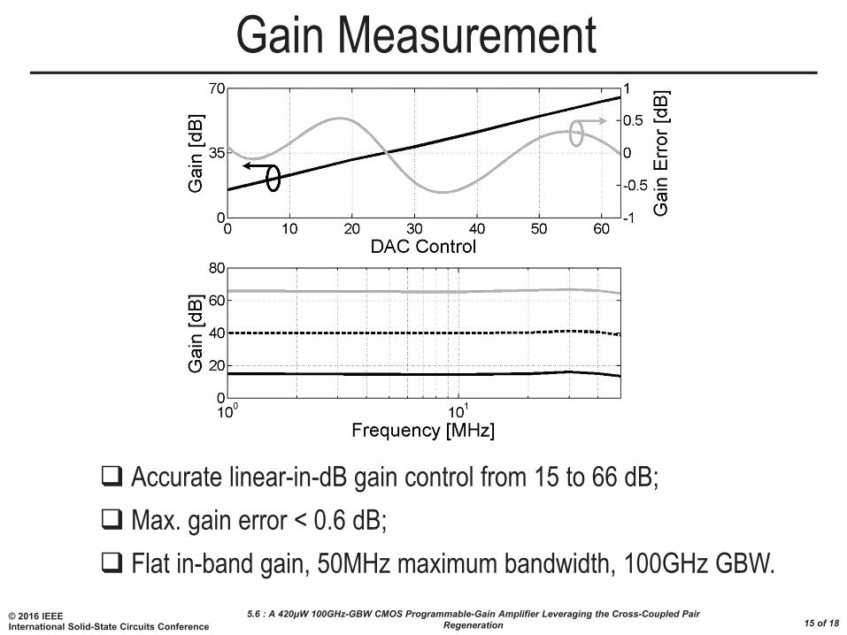
Gain Measurement
Accurate linear-in-dB gain control from 15 to 66 dB;
Max. gain error < 0.6 dB;
Flat in-band gain, 50MHz maximum bandwidth, 100GHz GBW.

5.6 : A 420 W 100GHz-GBW CMOS Programmable-Gain Amplifier Leveraging the Cross-Coupled Pair
Regeneration© 2016 IEEE International Solid-State Circuits Conference 16 of 18
Linearity Measurement
OP1dB = -2 dBV @ 45dB gain;
THD < -40dB from 10dB back off down;
OIP3 = 4.3 dBV calculated from IM3 test.

5.6 : A 420 W 100GHz-GBW CMOS Programmable-Gain Amplifier Leveraging the Cross-Coupled Pair
Regeneration© 2016 IEEE International Solid-State Circuits Conference 17 of 18
Summary of the PerformanceJSSC-13 TCAS-14 JSSC-15 This work
Technology 65nm 150nm 180nm 180nm
Active Area [mm2] 0.01 0.05 0.07 0.03
Gain Range [dB] -13 / 63 -5.5 / 28 3.6 / 59.6 15 / 66
dB-linear Gain Range [dB] 50 34 56 51
OP1dB [dBm] - 5.6 -3 8
OIP3 [dBm] 11.5 13 / 17.3 8 14.3
Input Noise [nV/(Hz)0.5] 3.5 11.14 10.6 10.7
Bandwidth [MHz] 14.8 60 63.5 50
GBW [GHz] 21 1.5 60.6 100
N of stages 3 1 15 1
Power [mW] 2.16 7.56 1.12 0.42
Highest OP1dB, state-of-the-art linearity and noise performance;
Record GBW with the lowest power consumption.

5.6 : A 420 W 100GHz-GBW CMOS Programmable-Gain Amplifier Leveraging the Cross-Coupled Pair
Regeneration© 2016 IEEE International Solid-State Circuits Conference 18 of 18
Conclusions
A sampled-time PGA leveraging the cross-coupled pair regeneration
has been presented;
Regeneration naturally leads to dB-linear gain control and
outperforms the linear GBW trade-off in a single stage;
Measurements demonstrate a record 100GHz GBW, the highest
OP1dB with state-of-the-art noise performance and lowest power
consumption.