a 9 a, addressable gen2 sensor tag for biosignal acquisition
TRANSCRIPT

2198 IEEE JOURNAL OF SOLID-STATE CIRCUITS, VOL. 45, NO. 10, OCTOBER 2010
A 9 �A, Addressable Gen2 Sensor Tagfor Biosignal Acquisition
Daniel Yeager, Student Member, IEEE, Fan Zhang, Student Member, IEEE, Azin Zarrasvand, Student Member, IEEE,Nicole T. George, Thomas Daniel, and Brian P. Otis, Senior Member, IEEE
Abstract—Biosensors present exciting opportunities in novelmedical and scientific applications. However, sensor tags presentedto date cannot interface with practical sensors, lack addressability,and/or require a custom (high-cost) interrogator. Our tag providesthese features via ultra-low-power circuitry including a low-noisebiosignal amplifier, unique tag ID generator, calibration-free3 MHz oscillator, and EPC C1 Gen2 protocol compatibility. In ad-dition to design details and measurement data from the fabricatedIC, we present in vivo muscle temperature measurement from anuntethered in-flight hawkmoth.
Index Terms—Biomedical, implantable electronics, RFID, lowpower, analog.
I. INTRODUCTION
C OMPELLING applications in both the scientific andmedical monitoring of biosignals have created a demand
for wireless, unobtrusive sensors to collect this data. Examplebiosignals include temperature, blood pressure, heart rate,blood glucose level, and neural activity. In scientific applica-tions, measurement of these biosignals helps researchers studycomplex biological systems, the effect of various diseases, andresearch treatments. In clinical settings, these signals are usedby a doctor or patient to either detect disease at onset or helpadminister treatment.
Measurement of biosignals presents several challenges. Mostimportantly, the sensor must be unobtrusive to the user. This in-volves minimizing the size and weight of the sensor as well asmaximizing the sensor lifespan. A means of wireless data col-lection is necessary for scientific research, where data shouldbe available in real-time, and for implantable medical biosen-sors where data is otherwise inaccessible. A number of solu-tions have been proposed including use of a small battery topower the sensor or an inductive link to power and communicatewith the sensor. Unfortunately, battery-powered sensors suffer
Manuscript received April 23, 2010; revised July 10, 2010; accepted July 17,2010. Date of current version September 24, 2010. This paper was approved byAssociate Editor Kenneth Shepard. This work was supported by the NationalScience Foundation ECS Award 0824265, the Komen Endowed Chair, the Of-fice of Naval Research (ONR) MURI grant to T. Daniel, and Intel Labs Seattle.
D. Yeager, F. Zhang, and B. Otis are with the Department of Electrical En-gineering, University of Washington, Seattle, WA 98195 USA e-mail: ([email protected]; http://wireless.ee.washington.edu).
A. Zarrasvand was with the Department of Electrical Engineering, Universityof Washington, Seattle, WA 98195 USA, and is now with the MicroelectronicsDepartment, Raytheon Corporation, Andover, MA 01810 USA.
N. George and T. Daniel are with the Department of Biology, University ofWashington, Seattle, WA 98195 USA.
Color versions of one or more of the figures in this paper are available onlineat http://ieeexplore.ieee.org.
Digital Object Identifier 10.1109/JSSC.2010.2063930
Fig. 1. Biosignal acquisition system.
from short lifespan due to the size and weight constraints of thebattery. Inductively-coupled devices suffer from short wirelessrange (on the order of cm).
We propose the use of passive radio frequency identifica-tion (RFID) technology to address many of the challenges ofbiosignal sensors. Most importantly, passive RFID allows wire-less, battery-free operation at meter ranges (see Fig. 1). Thisenables wearable and implantable biosensors with an unlim-ited lifespan, small size, and sub-gram weight. Many passivesensor tags reported to date have employed simple ring oscil-lator temperature sensors with no protocol or addressability.However, realistic applications demand accurate processing of
V-level biosignals and compatibility with industry standardRFID protocols.
We present a fully-passive 900 MHz RFID tag IC withaddressability, full EPC Class 1 Generation 2 (Gen2) protocolcompatibility, a 1.25 V integrated noise chopper-stabi-lized micropower sensor interface amplifier, and an 8b ADC.The communication range is 3 m with an off-the-shelf RFIDreader, enabling previously impossible recording scenarios likein-flight recording from small insects. A significant improve-ment in performance beyond the state-of-the-art was achievedby utilizing a novel self-calibrating on-chip frequency refer-ence, subthreshold digital logic, a low-noise chopper amplifier,8b ADC, and a unique chip ID generator.
II. PRIOR WORK
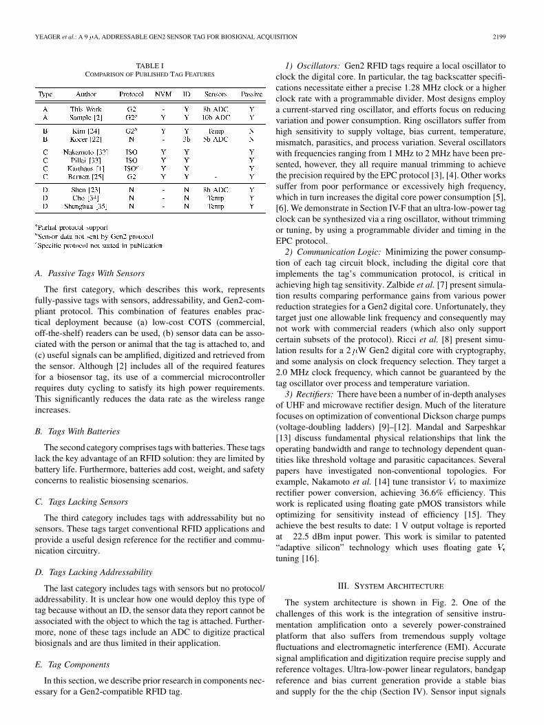
A plethora of RFID-related research has appeared in theliterature, predominately since Karthaus’ [1] influential andwidely-cited paper in 2003. The recent technological feasi-bility of RFID, coupled with numerous application spaces andwidespread commercial adoption, have galvanized academicresearch in this field. A number of full tag implementationshave been presented in the literature, and they are grouped byfeature set in Table I.
0018-9200/$26.00 © 2010 IEEE
YEAGER et al.: A 9 A, ADDRESSABLE GEN2 SENSOR TAG FOR BIOSIGNAL ACQUISITION 2199
TABLE ICOMPARISON OF PUBLISHED TAG FEATURES
A. Passive Tags With Sensors
The first category, which describes this work, representsfully-passive tags with sensors, addressability, and Gen2-com-pliant protocol. This combination of features enables prac-tical deployment because (a) low-cost COTS (commercial,off-the-shelf) readers can be used, (b) sensor data can be asso-ciated with the person or animal that the tag is attached to, and(c) useful signals can be amplified, digitized and retrieved fromthe sensor. Although [2] includes all of the required featuresfor a biosensor tag, its use of a commercial microcontrollerrequires duty cycling to satisfy its high power requirements.This significantly reduces the data rate as the wireless rangeincreases.
B. Tags With Batteries
The second category comprises tags with batteries. These tagslack the key advantage of an RFID solution: they are limited bybattery life. Furthermore, batteries add cost, weight, and safetyconcerns to realistic biosensing scenarios.
C. Tags Lacking Sensors
The third category includes tags with addressability but nosensors. These tags target conventional RFID applications andprovide a useful design reference for the rectifier and commu-nication circuitry.
D. Tags Lacking Addressability
The last category includes tags with sensors but no protocol/addressability. It is unclear how one would deploy this type oftag because without an ID, the sensor data they report cannot beassociated with the object to which the tag is attached. Further-more, none of these tags include an ADC to digitize practicalbiosignals and are thus limited in their application.
E. Tag Components
In this section, we describe prior research in components nec-essary for a Gen2-compatible RFID tag.
1) Oscillators: Gen2 RFID tags require a local oscillator toclock the digital core. In particular, the tag backscatter specifi-cations necessitate either a precise 1.28 MHz clock or a higherclock rate with a programmable divider. Most designs employa current-starved ring oscillator, and efforts focus on reducingvariation and power consumption. Ring oscillators suffer fromhigh sensitivity to supply voltage, bias current, temperature,mismatch, parasitics, and process variation. Several oscillatorswith frequencies ranging from 1 MHz to 2 MHz have been pre-sented, however, they all require manual trimming to achievethe precision required by the EPC protocol [3], [4]. Other workssuffer from poor performance or excessively high frequency,which in turn increases the digital core power consumption [5],[6]. We demonstrate in Section IV-F that an ultra-low-power tagclock can be synthesized via a ring oscillator, without trimmingor tuning, by using a programmable divider and timing in theEPC protocol.
2) Communication Logic: Minimizing the power consump-tion of each tag circuit block, including the digital core thatimplements the tag’s communication protocol, is critical inachieving high tag sensitivity. Zalbide et al. [7] present simula-tion results comparing performance gains from various powerreduction strategies for a Gen2 digital core. Unfortunately, theytarget just one allowable link frequency and consequently maynot work with commercial readers (which also only supportcertain subsets of the protocol). Ricci et al. [8] present simu-lation results for a 2 W Gen2 digital core with cryptography,and some analysis on clock frequency selection. They target a2.0 MHz clock frequency, which cannot be guaranteed by thetag oscillator over process and temperature variation.
3) Rectifiers: There have been a number of in-depth analysesof UHF and microwave rectifier design. Much of the literaturefocuses on optimization of conventional Dickson charge pumps(voltage-doubling ladders) [9]–[12]. Mandal and Sarpeshkar[13] discuss fundamental physical relationships that link theoperating bandwidth and range to technology dependent quan-tities like threshold voltage and parasitic capacitances. Severalpapers have investigated non-conventional topologies. Forexample, Nakamoto et al. [14] tune transistor to maximizerectifier power conversion, achieving 36.6% efficiency. Thiswork is replicated using floating gate pMOS transistors whileoptimizing for sensitivity instead of efficiency [15]. Theyachieve the best results to date: 1 V output voltage is reportedat 22.5 dBm input power. This work is similar to patented“adaptive silicon” technology which uses floating gatetuning [16].
III. SYSTEM ARCHITECTURE
The system architecture is shown in Fig. 2. One of thechallenges of this work is the integration of sensitive instru-mentation amplification onto a severely power-constrainedplatform that also suffers from tremendous supply voltagefluctuations and electromagnetic interference (EMI). Accuratesignal amplification and digitization require precise supply andreference voltages. Ultra-low-power linear regulators, bandgapreference and bias current generation provide a stable biasand supply for the the chip (Section IV). Sensor input signals

2200 IEEE JOURNAL OF SOLID-STATE CIRCUITS, VOL. 45, NO. 10, OCTOBER 2010
Fig. 2. Block diagram of the system.
(e.g., EEG, EMG, thermocouple) are first amplified with theon-chip low-noise chopper-stabilized amplifier (Section V). An8b SAR ADC then digitizes the sensor data. The sensor data isassociated with a person or animal by means of a unique tagID (UID). This UID leverages process variation in the startupconfiguration of an SRAM, thus eliminating the need fornon-volatile memory [17]. Random numbers (RN) are requiredin the Gen2 protocol for anticollision and (weak) encryptionof reader-to-tag data. These are generated by sampling the(unpredictable) clock phase at the downlink baseband edgesand passing it through an LFSR. Finally, the on-chip controllerlogic encodes the RN, UID, and ADC data into a Gen2-com-patible packet in response to reader commands (Query/ReqRN,Ack, and Read, respectively) (Section VI). The UID and sensordata are available for real-time use by a PC through an ethernetconnection to the reader.
IV. ANALOG CORE
The analog core is responsible for generating accurate biascurrents and voltages for the chip, which in turn enables accuratebiosignal amplification and digitization. Total measured powerconsumption for the analog blocks is 1.2 A. The various circuitblocks are described in the following subsections:
A. Rectifier
The RF rectifier employs a 6-stage voltage-doubling chargepump topology. High sensitivity and efficiency are achieved byusing zero- diode-connected nMOS devices. Measured per-formance is plotted in Fig. 3. An off-chip L-match networktransforms the impedance to 50 ; alternately, this matchingnetwork can be easily absorbed into the antenna as in commer-cial designs.
B. Bias Current Generation
Bias currents for the chip are generated by a 45 nA ref-erence, shown in Fig. 4. Despite the use of thick-oxide devices(which allow up to 3.6 V unregulated supply voltage), the biasgenerator starts reliably at 0.6 V. The high output impedance ofthe cascode devices maintains a constant output current of 45 nA
Fig. 3. Measured rectifier efficiency versus output voltage and input power.
from 0.6 V to 3.6 V as shown in Fig. 5(a). Process and mis-match variation is minimized through use of relatively-large de-vice sizes as well as precision resistors. Simulated Monte Carlovariation is 2.8 nA (6%) without trimming [see Fig. 5(b)]. Mea-sured bias current consumption for the full analog core corre-sponded well with the anticipated current based on simulationof the bias current reference.
Many startup circuits for bias current references consumesignificant static current. The startup circuit shown in Fig. 4uses MOS-bipolar pseudo-resistors (M2, M3) as an area-effi-cient means of creating very large resistances (e.g., 100 G ),which minimize static current. A 200 fF capacitor provides fasttransient startup when the circuit is powered on and preventsoscillation of the startup circuitry. In addition, supply noise willnot cause disturbances in steady-state operation because thegates of M5 and M7 are pulled to ground. Transistors M1, M2,and M4 ensure that the gates of M5 and M7 are fully dischargedin spite of off-resistance variation across process corners.
C. Bandgap Reference and Supply Regulation
A stable reference voltage is obtained through an ultra-low-power bandgap reference, shown in Fig. 6(a). The total supplycurrent is 220 nA, and the measured output voltage is stable towithin 4 mV of the nominal 1.2 V across 0–100 C.
Three low-drop-out linear regulators provide stable suppliesfor the 0.7 V digital core, the 1.2 V analog core, and an auxiliary1.8 V supply for any off-chip ICs, respectively. The 1.2 V and

YEAGER et al.: A 9 A, ADDRESSABLE GEN2 SENSOR TAG FOR BIOSIGNAL ACQUISITION 2201
Fig. 4. Bias current generator schematic.
Fig. 5. Bias current generator performance. (a) Simulated bias current versus supply voltage. (b) Simulated Monte Carlo bias current distribution (process andmismatch).
1.8 V regulators utilize the bandgap voltage reference voltage,which provides a precise, temperature-independent voltage ref-erence for the biosignal amplifier and ADC. The 0.7 V regulatoris generated by sensing the transistor . This creates a CTATsupply voltage that automatically compensates for process andtemperature variation in the digital blocks.
The regulators employ a straightforward single-stage op-ampwith 60 dB gain and 100 nA current consumption. The 0.7 Vand 1.2 V regulators use unity-gain feedback, while the 1.8 Vuses resistive feedback. On-chip mega-ohm resistors are used in1.8 V regulator feedback network to limit the quiescent current.Low precision (but well-matched) resistors can be afforded be-cause the ratio, not the absolute value, of two resistors sets theaccuracy of the output voltage.
D. Demodulator
Reader-to-tag communication employs pulse-intervalencoding (PIE). Specifically, the duration of the positivepulsewidth determines whether each bit is a zero or one. Posi-tive pulses are delineated by a short negative pulse of duration
PW, which is as small as 1.66 s. This sets the lower limit onthe demodulator bandwidth to approximately 1.2 MHz.
The digital core measures and converts the positive pulse du-rations into data and clock. However, the received signal (theoutput of the rectifier) is not a suitable digital signal due to thefinite time constants in the rectifier. The purpose of the demod-ulator is to recover a logic-level (rail to rail) signal from the rec-tifier output. The demodulator inputs are the rectifier output anda low-pass-filtered version of the rectifier output. The low-passfilter has an approximately 16 kHz bandwidth to filter out thenegative pulses.
The demodulator schematic is shown in Fig. 8. The firststage provides differential to single-ended conversion. Thesecond stage significantly boosts the signal swing in order toachieve logic level voltages. Thick-oxide buffers with a lowsupply voltage (0.7 V) prevent crowbar current that could resultfrom the limited slew rate of the low-power comparator. Thedifferential pair is biased with 75 nA, and the common-sourcestage is biased with 300 nA which only draws current when thereader carrier is on. The unity gain bandwidth of demodulatoris set to 2 MHz. This ensures reliable recovery of the input

2202 IEEE JOURNAL OF SOLID-STATE CIRCUITS, VOL. 45, NO. 10, OCTOBER 2010
Fig. 6. Bias voltage and supply generation schematics. (a) Bandgap reference schematic. (b) Voltage regulator schematic.
Fig. 7. Measured regulator performance. (a) Line regulation for the 1.8 V (top), 1.2 V (middle) and 0.7 V (bottom) regulators. (b) Load regulation.
Fig. 8. Analog demodulator that is used to recover a logic-level baseband signal from the rectifier output.
signal (up to 1.2 MHz) under a wide range of temperature andprocess corners.
E. Modulator
RFID tags communicate with the interrogator by either ab-sorbing or reflecting the RF carrier sent by the interrogator. A
single transistor switch is used to modulate the tag reflectioncoefficient. A thick-oxide (IO) high- device is used to pre-vent breakdown when the tag is near the reader (at which pointgreater than 10 dBm can be expected at the tag antenna). Ex-perimental results demonstrate that the tag is downlink limited,and the return loss with the modulator enabled is 0.6 dB.

YEAGER et al.: A 9 A, ADDRESSABLE GEN2 SENSOR TAG FOR BIOSIGNAL ACQUISITION 2203
Fig. 9. Three-stage ring oscillator schematic and prescale divider.
Fig. 10. Oscillator performance versus temperature and divider operation. The red dashed lines denote the acceptable residual error as per the EPC specification.(a) Measured and simulated oscillator frequency versus temperature. (b) Divider output residual error versus input (oscillator) frequency.
F. Oscillator
Many tags use a 1.5 MHz clock, which requires the tag oscil-lator PVT stability to meet Gen2 timing specifications ( 15%for 640 kHz uplink) as the integer divider residual exceeds theallotted tolerance. Resistor trimming [4], bias current tuning[3], phase locking, and quartz references have been proposedto compensate for PVT variation but are prohibitive due to cost,power and size constraints. We propose a 3 MHz temperature-stabilized ring oscillator, shown in Fig. 9, which lowers the di-vider residual such that PVT compensation can be performedby the integer divider. The oscillator consumes 260 nA from the0.7 V digital supply. We take three approaches to improve sta-bility. First, large device size and careful layout limit processvariation to 13% (measured, Fig. 10(a)). Second, the dividerresidual is centered at zero, which reduces the peak residual bya factor of 2 (Fig. 10). Third, a novel temperature compensationshown in Fig. 9 tunes the oscillator bias current by measuringand compensating the temperature coefficient. As tempera-ture decreases, decreases. The negative coeffi-cient increases the current through , providing the oscil-lator increased current to compensate for the temperature vari-ation. Careful design of the transistor inversion coefficient andvalue of , results in a first-order temperature coefficientcancellation.
G. ADC
An 8-bit successive-approximation register (SAR) ADC dig-itizes the amplified biosignals. Virtually no static current is con-sumed through the use of a discrete-time comparator. Completetesting and characterization of the ADC is presented in [18].
H. Unique ID Generation
In order to associate sensor data from a tag with the objectthat the tag is attached to, the tag must have a unique ID. Tra-ditionally, the tag is manually programmed with a specified IDby the interrogator, which is stored in a non-volatile memory(NVM) such as flash, EEPROM, or resistor fuse array. How-ever, these NVM require large voltages and currents, which inturn degrade tag performance due to increased power consump-tion. We instead employ lithographic uncertainty and randomdopant fluctuation to create a unique, random ID for each tag[17]. Specifically, the tag reads the power-on state of a 128-bitSRAM array. This technique allows reliable identification ofICs without explicit programming steps. On average, 95% of thebits are stable, and unstable bits are easily filtered out via appli-cation-level software. Note that unstable ID bits do not impairGen2 protocol compatibility due to the use of random numbersas tag handles.

2204 IEEE JOURNAL OF SOLID-STATE CIRCUITS, VOL. 45, NO. 10, OCTOBER 2010
Fig. 11. Schematic of fully-differential chopper-stabilized low-noise amplifier. Compensation capacitors and nulling resistors are not included for simplicity.
Fig. 12. Chopper amplifier architecture.
V. BIOSIGNAL AMPLIFIER
A. Chopper-Stabilized Low-Noise Amplifier Design
Our multi-purpose sensing tag is designed for a variety ofsensor interfaces, including biosignal detection, thermocouplereadout, and gas detection. These applications demand an ex-tremely low noise floor ( 2 V input referred) under a rel-atively low bandwidth ( 1 kHz). When the signals of interestfall below a few hundred Hertz, the dominating circuit noisesshift from the thermal noise to 1/f and popcorn noise [19]. Ex-cess low-frequency noise can undermine the system’s signal-to-noise ratio (SNR) and cause errors in the measurement. As a re-sult, we use a chopper-stabilized topology to suppress 1/f noiseand offset that plague sub-micron CMOS processes.
Closed-loop chopper-stabilization has been adopted recently[20], [21], [19] to suppress gain and sensitivity errors, as wellas to prevent saturation due to amplifier offset. Among the re-cent implementations, [19] provides the best figure-of-merit sofar. AC feedback is employed to ensure all signals entering theamplifier are well above 1/f noise corner. However, separate ac-tive input-biasing circuitry is used, and higher supply voltage isrequired due to single-ended approach.
As shown in Figs. 11 and 12, we employ a fully-differentialclosed-loop architecture to ensure sufficient linearity and supplyrejection. Operating transistors in the subthreshold region en-ables the use of a power-efficient telescopic-cascode op-amptopology under low supply voltages. Signal up-conversion oc-curs at the gate of the input transistors, which are biased in weakinversion to maximize the transconductance. We introduce a

YEAGER et al.: A 9 A, ADDRESSABLE GEN2 SENSOR TAG FOR BIOSIGNAL ACQUISITION 2205
Fig. 13. Measured transfer function and noise plot of the low-noise chopper-stabilized biosignal amplifier. (a) Chopper-Amplifier Gain Magnitude Plot,(b) Chopper-Amplifier Noise Plot.
Fig. 14. EPC Gen2 digital core with sensor data interface.
novel dual-feedback technique to simultaneously set the mid-band gain of the amplifier through , and bias the amplifier’sinput node through high-resistance pseudo-resistors. Chopperswitches are included in both the signal and biasing paths to notonly guarantee negative feedback around the amplifier, but alsoavoid using additional input-biasing circuitry as in [19]. Werealize the chopper modulator with a minimally-sized CMOStransmission gate to minimize charge injection. The inputcapacitance is 15 pF. When modulated with a 10 kHzchopper clock, the input impedance (1.06 M ) is high enoughto avoid loading the electrodes for biomedical applications. Theratio of and establishes a 40 dB midband gain. issized slightly smaller (140 fF) to take into account the additionof parasitic and switch capacitances.
Two additional sets of chopper switches are added in the firststage of the amplifier: one set of switches is placed at the drainsof the input transistors to demodulate the ac signal down to base-band and modulate the input offsets up to the chopper frequency;another pair is placed at the drains of the pMOS current sourceto modulate their flicker noise up to a higher frequency. At theoutput of the amplifier, the signal returns to baseband while theoffsets and flicker noise are modulated up to high frequency andthen filtered by the amplifier’s second stage. The second stageis implemented as common-source to increase the output swingunder low supply voltages. The output is then fed back to thesumming node at the input of the amplifier after being modu-lated up to the chopper frequency. In order to avoid large passivedevices, we implemented continuous-time tunable Gm-C filtersto reduce ripple at the output of the amplifier. The input-referrednoise from the ripple filter (Gm-C filters) is designed to be negli-
gible. The six achievable bandwidths of the Gm-C filters are log-arithmically spread between 150 Hz to 400 Hz. The tunabilityof the filters is realized through digital control of the transcon-ductor current.
B. Low-Noise Amplifier Measurement Results
Fig. 13(a) plots the gain magnitude with chopping on andoff. The midband gain for both cases is approximately 38.5 dB.When the chopper clock is off, the amplifier operates as a con-ventional AC-coupled amplifier and has a high-pass corner of0.2 Hz. Amplification is preserved down to DC when chopper-stabilization is enabled. The tunable low-pass corner is set to230 Hz in this measurement.
Fig. 13(b) illustrates the input-referred noise of the amplifierwith chopping on and off. Low frequency spot noise is reducedby more than a decade when the chopper is enabled. The mea-sured integrated noise from 0.05 Hz to 100 Hz is 1.25 Vwhen the chopper switches are on, compared to 4.46 Vwhen the chopper switches are off.
VI. DIGITAL CORE
A high level block diagram of the digital core is shown inFig. 14. The Receive block performs clock and data recovery(CDR) on the PIE signal. A Packet Parse block decodes EPCcommands and stores relevant information for the Controllerand Prescaler. The Controller block decides what packet tosend after receiving a packet from the reader, and enables thetransmitter logic if appropriate. The Sequencer constructs an

2206 IEEE JOURNAL OF SOLID-STATE CIRCUITS, VOL. 45, NO. 10, OCTOBER 2010
Fig. 15. EPC Gen2-compliant sensor data protocol.
TABLE IISENSOR TAG PERFORMANCE
Fig. 16. Schematic of the cross section of Manduca dorsolongitudinal muscletemperature measurement.
EPC-compliant packet including preamble and CRC, and theEncoder converts the data bit stream to Miller or FM0 encoding.
VII. SENSOR DATA PROTOCOL
Interoperability with COTS readers requires Gen2 protocolcompatibility. Fig. 15 illustrates how the protocol works andhow sensor data is retrieved. The Query and ReqRN commandsimplement anticollision in the protocol. These commands re-quire random numbers, which are generated by sampling the(unpredictable) clock phase at the downlink baseband edges andpassing it through an LFSR. The tag identifier (ID) is queried viathe Ack command, and the ID is generated by the UID, as de-scribed in Section IV.H. Finally, sensor data is returned throughthe Read command. An example measured ID returned by oneof our tags is shown in Fig. 15.
VIII. PERFORMANCE
This system was fabricated in a 0.13 m CMOS process.The die photo is shown in Fig. 19. A ground shield made ofthe 4- m-thick top aluminum metal covers the entire die toreduce the impact of EMI, capacitive, and light sensitivityon the extremely high impedance internal instrumentationnodes. First-silicon functionality was ensured through exten-sive FPGA testing of the digital core with a commercial RFIDreader through a passive RFID analog front end composed of
Fig. 17. Measured temperature versus time from a tethered moth.
Fig. 18. Measured temperature versus time from an untethered moth.
Fig. 19. Chip and board micrographs.
discrete COTS ICs (see [2] for a schematic). Mixed signal sim-ulations were performed to verify the communication interfacesbetween the digital core and the analog blocks (UID, ADC, anddemodulator).
Table II compares the performance of this work to other tagspresented in the literature. For a comparison of tag features,

YEAGER et al.: A 9 A, ADDRESSABLE GEN2 SENSOR TAG FOR BIOSIGNAL ACQUISITION 2207
Fig. 20. Photograph showing an untethered moth with the RFID measurement sensor.
refer back to Table I. This work compares favorably to othersensor tags without resorting to duty cycling [2], [22], lossof Gen2 compatibility [23], or elimination of the ADC [24].Drawing comparisons to tags lacking sensors and/or address-ability (all remaining tags) is less meaningful, but [1] and [25]clearly achieve the best RF sensitivity for a fully-passive tag.In part, our use of a linear regulator, ADC and more complexstate machine simply limit the achievable sensitivity.
IX. IN VIVO, IN-FLIGHT BIOSIGNAL ACQUISITION
The ability to monitor in vivo biosignals such as temperatureand motor patterns in an organism without altering the kine-matic output is invaluable to many fields of biology, and is par-ticularly important in understanding the control of movementin humans and other animals. Currently, there is only a generalunderstanding of how temperature affects muscle performance.Though the temperature dependence of muscle contraction hasalready been established from in vitro preparations, the ability tocorrelate locomotor and kinematic performance with body tem-perature has thus far been hindered by obtrusive sensors [26],[27].
The hawkmoth, Manduca sexta, provides a well-documentedmodel system in which to develop an understanding betweenbiosignal output and behavior. Like other endotherms, Manducautilizes the heat released from synchronous isometric musclecontractions to generate an elevated core temperature [28]. In-creased muscle temperature allows these insects to increase theirwing beat frequency and thus produce greater mechanical poweroutput [29].
We used our sensing tag with a COTS RFID reader to recordthe in-flight temperature of the dominant flight muscles ofManduca (the dorsolongitudinal muscles: DLM sensu [30]).The copper-constantan thermocouple was inserted into theDLM , approximately 3 mm below the dorsal aspect of the cu-ticle (Fig. 16). Using the instantaneous read-out of our wirelesssensor, we can correlate the rate of heat production during flight
TABLE IIICOMPARISON OF PUBLISHED (MEASURED) TAG PERFORMANCE
Duty cycling required at this input power.Calculated based on 20% rectifier efficiency and 50% modulation losses.Process includes Schottky diodes.No power numbers reported, but authors claim 36.6% rectifier efficiency and
4.3m range given 4W EIRP.Simulation result, no measurements reported.
TABLE IVRFID SENSOR SPECIFICATIONS
with the observed kinematic response. Both rapid and largescale changes in body temperature will reveal how Manducathermoregulates according to its energetic requirements.
Results from tethered and untethered temperature mea-surements show that the temperature of the DLM increasedwith time, stabilizing around 29 C for the tethered moth and30–35 C for the untethered moth (Figs. 17 and 18). Becausethe behavior of the moth is uncontrolled, the untethered datashow the moth resting at the 4 minute and 7 minute time marks.The tethered data represent one continued period of activity by
2208 IEEE JOURNAL OF SOLID-STATE CIRCUITS, VOL. 45, NO. 10, OCTOBER 2010
the moth. The temperature is different between the two trialsdue to different implant depths of the thermocouple as well asdifferent characteristics of the moth.
Fig. 19 shows the PCB used for this experiment, whichmeasures less than 1 cm and weighs 0.25 g. Additional ther-mocouple gain is achieved using on-board 1.8 V micropoweropamps that are powered from our on-chip 1.8 V regulators. Aphotograph of the moth wearing the system is shown in Fig. 20.Including the antenna and thermocouple, the entire systemweighs 0.35 g. Full system specifications are listed in Table IV.The power of our moth-worn system is two orders of magnitudelower than an active radio- based tag [31]. This work enablesthe first long-term in-flight recording of an insect by removingboth the wires and batteries from the recording equipment.
X. CONCLUSION
For many wirelessly-deployed sensors, periodic batteryreplacement is costly at best and infeasible at worst. Two keyfeatures of RFID make it attractive for wireless sensor de-ployment: power is wirelessly and deliberately supplied to thetag, and backscatter modulation allows for nearly-zero powertag-to-reader communication. Coupling this technology withbiomedical applications promises exciting advances in medicaldelivery. Specifically, Gen2 compatibility, tag addressability,and the ability to interface with useful sensors will enable thesebiosensors to be deployed as medical and research tools.
Our multi-purpose sensing tag was designed for a variety ofsensor interfaces such as such as EMG (electromyograms), ther-mocouple readout, and gas detection. These applications de-mand an extremely low noise floor ( 2 V input referred)under a relatively low bandwidth ( 1 kHz). Furthermore, thetag lifespan should not be limited by battery life. This paperdemonstrates the feasibility of in vivo, untethered, in-flight tem-perature recording of insects. The key novelty is that this long-term wireless recording was previously unattainable due to thesize, weight, and lifespan of conventional sensors.
REFERENCES
[1] U. Karthaus and M. Fischer, “Fully integrated passive UHF RFIDtransponder IC with 16.7-�W minimum RF input power,” IEEE J.Solid-State Circuits, vol. 38, no. 10, pp. 1602–1608, Oct. 2003.
[2] A. P. Sample, D. J. Yeager, P. S. Powledge, A. V. Mamishev, and J. R.Smith, “Design of an RFID-based battery-free programmable sensingplatform,” IEEE Trans. Instrumentation and Measurement, vol. 57, no.11, pp. 2608–2615, Nov. 2008.
[3] F. Cilek, K. Seemann, D. Brenk, J. Essel, J. Heidrich, R. Weigel, andG. Holweg, “Ultra low power oscillator for UHF RFID transponder,”in Proc. 2008 IEEE Int. Frequency Control Symp., May 2008, pp.418–421.
[4] R. Barnett and J. Liu, “A 0.8 V 1.52 MHz MSVC relaxation oscillatorwith inverted mirror feedback reference for UHF RFID,” in Proc. IEEECustom Integrated Circuits Conf. (CICC’06), Sep. 2006, pp. 769–772.
[5] C. Klapf, A. Missoni, W. Pribyl, G. Holweg, and G. Hofer, “Analysesand design of low power clock generators for RFID TAGs,” in Researchin Microelectronics and Electronics 2008 (PRIME 2008), Apr. 2008,pp. 181–184.
[6] F. Song, J. Yin, H. Liao, and R. Huang, “Ultra-low-power clock gen-eration circuit for EPC standard UHF RFID transponders,” ElectronicsLett., vol. 44, no. 3, pp. 199–201, 2008, 31.
[7] I. Zalbide, J. Vicario, and I. Velez, “Power and energy optimization ofthe digital core of a Gen2 long range full passive RFID sensor tag,” inProc. 2008 IEEE Int. Conf. RFID, Apr. 2008, pp. 125–133.
[8] A. Ricci, M. Grisanti, I. De Munari, and P. Ciampolini, “Design of a2 �W RFID baseband processor featuring an AES cryptography prim-itive,” in Proc. 15th IEEE Int. Conf. Electronics, Circuits and Systems(ICECS 2008), Sep. 2008, pp. 376–379.
[9] T. Umeda, H. Yoshida, S. Sekine, Y. Fujita, T. Suzuki, and S. Otaka,“A 950 MHz rectifier circuit for sensor networks with 10 m-distance,”in 2005 IEEE Int. Solid-State Circuits Conf. (ISSCC) Dig. Tech. Papers,Feb. 2005, vol. 1, pp. 256–597.
[10] G. De Vita and G. Iannaccone, “Design criteria for the RF section ofUHF and microwave passive RFID transponders,” IEEE Trans. Mi-crow. Theory Tech., vol. 53, no. 9, pp. 2978–2990, Sep. 2005.
[11] R. Barnett, S. Lazar, and J. Liu, “Design of multistage rectifiers withlow-cost impedance matching for passive RFID tags,” in 2006 IEEERadio Frequency Integrated Circuits (RFIC) Symp. Dig. Papers, Jun.2006, p. 4.
[12] J. Yi, W.-H. Ki, and C.-Y. Tsui, “Analysis and design strategy of UHFmicro-power CMOS rectifiers for micro-sensor and RFID applica-tions,” IEEE Trans. Circuits Syst. I: Reg. Papers, vol. 54, no. 1, pp.153–166, Jan. 2007.
[13] S. Mandal and R. Sarpeshkar, “Low-power CMOS rectifier design forRFID applications,” IEEE Trans. Circuits Syst. I: Reg. Papers, vol. 54,no. 6, pp. 1177–1188, Jun. 2007.
[14] H. Nakamoto, D. Yamazaki, T. Yamamoto, H. Kurata, S. Yamada, K.Mukaida, T. Ninomiya, T. Ohkawa, S. Masui, and K. Gotoh, “A passiveUHF RFID tag LSI with 36.6% efficiency CMOS-only rectifier andcurrent-mode demodulator in 0.35 �m FeRAM technology,” in 2006IEEE Int. Solid-State Circuits Conf. (ISSCC) Dig. Tech. Papers, Feb.2006, pp. 1201–1210.
[15] T. Le, K. Mayaram, and T. Fiez, “Efficient far-field radio frequencyenergy harvesting for passively powered sensor networks,” IEEE J.Solid-State Circuits, vol. 43, no. 5, pp. 1287–1302, May 2008.
[16] R. Glidden, C. Bockorick, S. Cooper, C. Diorio, D. Dressler, V. Gutnik,C. Hagen, D. Hara, T. Hass, T. Humes, J. Hyde, R. Oliver, O. Onen, A.Pesavento, K. Sundstrom, and M. Thomas, “Design of ultra-low-costUHF RFID tags for supply chain applications,” IEEE Commun. Mag.,vol. 42, no. 8, pp. 140–151, Aug. 2004.
[17] Y. Su, J. Holleman, and B. Otis, “A digital 1.6 pJ/bit chip identificationcircuit using process variations,” IEEE J. Solid-State Circuits, vol. 43,no. 1, pp. 69–77, Jan. 2008.
[18] J. Holleman, A. Mishra, C. Diorio, and B. Otis, “A micro-power neuralspike detector and feature extractor in. 13 �m CMOS,” in Proc. IEEECustom Integrated Circuits Conf. (CICC 2008), 2008, pp. 333–336.
[19] T. Denison, K. Consoer, W. Santa, A. Avestruz, J. Cooley, and A. Kelly,“A 2�W 100nV/
�Hz chopper-stabilized instrumentation amplifier for
chronic measurement of neural field potentials,” IEEE J. Solid-StateCircuits, vol. 42, no. 12, pp. 2934–2945, Dec. 2007.
[20] K. Makinw and J. Huijsing, “A wind sensor with an integrated low-offset instrumentation amplifier,” in Proc. 8th IEEE Int. Conf. Elec-tronics, Circuits and Systems (ICECS 2001), 2001, pp. 1505–1508.
[21] R. Yazicioglu, P. Merken, R. Puers, and C. Van Hoof, “A 60�W60nV/
�Hz readout front-end for portable biopotential acquisition
systems,” IEEE J. Solid-State Circuits, vol. 42, no. 5, pp. 1100–1110,May 2007.
[22] F. Kocer and M. Flynn, “A new transponder architecture with on-chipADC for long-range telemetry applications,” IEEE J. Solid-State Cir-cuits, vol. 41, no. 5, pp. 1142–1148, May 2006.
[23] H. Shen, L. Li, and Y. Zhou, “Fully integrated passive UHF RFID tagwith temperature sensor for environment monitoring,” in Proc. 7th Int.Conf. ASIC (ASICON’07), Oct. 2007, pp. 360–363.
[24] S. Kim, J.-H. Cho, H.-S. Kim, H. Kim, H.-B. Kang, and S.-K.Hong, “An EPC Gen2 compatible passive/semi-active UHF RFIDtransponder with embedded FeRAM and temperature sensor,” in Proc.IEEE Asian Solid-State Circuits Conf. (ASSCC’07), Nov. 2007, pp.135–138.
[25] R. Barnett, G. Balachandran, S. Lazar, B. Kramer, G. Konnail, S. Ra-jasekhar, and V. Drobny, “A passive UHF RFID transponder for EPCGen2 with �14 dBm sensitivity in 0.13 �m CMOS,” in 2007 IEEEInt. Solid-State Circuits Conf. (ISSCC) Dig. Tech. Papers, Feb. 2007,pp. 582–623.
[26] A. Bennett, “Thermal dependence of muscle function,” Amer. J.Physiol.—Regulatory, Integrative and Comparative Physiology, vol.247, no. 2, p. 217, 1984.
[27] R. Josephson, “Contraction dynamics of flight and stridulatory musclesof Tettigoniid insects,” J. Experiment. Biol., vol. 108, no. 1, p. 77, 1984.
[28] B. Heinrich, “Thermoregulation in endothermic insects,” Science, vol.185, no. 4153, p. 747, 1974.

YEAGER et al.: A 9 A, ADDRESSABLE GEN2 SENSOR TAG FOR BIOSIGNAL ACQUISITION 2209
[29] R. Stevenson and R. Josephson, “Effects of operating frequency andtemperature on mechanical power output from moth flight muscle,” J.Experiment. Biol., vol. 149, no. 1, p. 61, 1990.
[30] Y. Kondoh and Y. Obara, “Anatomy of motoneurones innervatingmesothoracic indirect flight muscles in the silkmoth, Bombyx mori,” J.Experiment. Biol., vol. 98, no. 1, p. 23, 1982.
[31] D. Daly, P. Mercier, M. Bhardwaj, A. Stone, Z. Aldworth, T. Daniel,J. Voldman, J. Hildebrand, and A. Chandrakasan, “A pulsed UWB re-ceiver SoC for insect motion control,” IEEE J. Solid-State Circuits, vol.45, no. 1, p. 153, Jan. 2010.
[32] H. Nakamoto, D. Yamazaki, T. Yamamoto, H. Kurata, S. Yamada, K.Mukaida, T. Ninomiya, T. Ohkawa, S. Masui, and K. Gotoh, “A pas-sive UHF RF identification CMOS tag IC using ferroelectric RAM in0.35-�m technology,” IEEE J. Solid-State Circuits, vol. 42, no. 1, pp.101–110, Jan. 2007.
[33] V. Pillai, H. Heinrich, D. Dieska, P. Nikitin, R. Martinez, and K. Rao,“An ultra-low-power long range battery/passive RFID tag for UHF andmicrowave bands with a current consumption of 700 nA at 1.5 V,” IEEETrans. Circuits Syst. I: Reg. Papers, vol. 54, no. 7, pp. 1500–1512, Jul.2007.
[34] N. Cho, S.-J. Song, S. Kim, S. Kim, and H.-J. Yoo, “A 5.1-�W UHFRFID tag chip integrated with sensors for wireless environmental mon-itoring,” in Proc. 31st European Solid-State Circuits Conf. (ESSCIRC2005), Sep. 2005, pp. 279–282.
[35] Z. Shenghua and W. Nanjian, “A novel ultra low power temperaturesensor for UHF RFID tag chip,” in Proc. IEEE Asian Solid-State Cir-cuits Conf. (ASSCC’07), Nov. 2007, pp. 464–467.
Daniel J. Yeager (S’05) received the B.S. degree(cum laude) and the M.S. degree in electrical engi-neering from the University of Washington, Seattle.He is currently working toward the Ph.D. degree inelectrical engineering at the University of Californiaat Berkeley.
During 2007, he worked at Intel Research Seattle,developing a programmable passive RFID tag that isnow used by over 30 research groups to study novelRFID applications. He has published in a broad rangeof RFID topics including encryption, neural and EEG
brain recording, strain measurement for aircraft and buildings, capacitive userinterfaces, and battery-free data logging. His research interests include wirelesssensing and energy scavenging, especially for biomedical applications.
Mr. Yeager’s work is supported by the National Science Defense and Engi-neering Grant.
Fan Zhang (S’08) received the B.S. degree inelectrical engineering and computer sciences fromthe University of California at Berkeley in 2007, andthe M.S. degree in electrical engineering from theUniversity of Washington, Seattle, in 2009. She iscurrently working toward the Ph.D. degree.
From 2006 to 2007, she interned at Agilent Tech-nologies, Santa Clara, CA. In 2009, she interned atIntel Corporations, Hillsboro, OR, and worked onmodeling of sigma-delta phase-locked loops. Hercurrent research interests include low-power analog
and RF circuit design for biomedical applications.Ms. Zhang was a corecipient of the 2010 DAC/ISSCC Student Design Contest
Award.
Azin Zarrasvand received the B.S.E.E. degreefrom the Iran University of Science and Technology,Tehran, Iran, in 1999, and the M.S.E.E. degree fromthe University of Washington, Seattle, in 2009.
Her interests are in low-power circuits and sys-tems. She has recently joined the MicroelectronicsDepartment at Raytheon Corporation, Andover, MA.
Nicole T. George received the Bachelor’s degree inbiology from the University of California at Berkeleyin 2006. She is currently pursuing the Ph.D. degree inthe Department of Biology at the University of Wash-ington, Seattle.
Her research currently focuses on the mechanicaland functional consequences of temperature gradi-ents within insect flight muscle.
Ms. George’s work is supported by the NSF Grad-uate Research Fellowship Program. She is a memberof the Society for Integrative and Comparative Bi-
ology and the Biophysical Society.
Thomas Daniel received the M.S. degree in biologyfrom the University of Wisconsin in 1978 and thePh.D. degree in biology from Duke University in1982.
From 1982 to 1984, he was the Bantrell Fellowin Engineering Sciences at the California Instituteof Technology. Since then, he has been on thefaculty in Biology at the University of Washington,Seattle, where he served as its inaugural chair during2001–2008. He is also Adjunct Professor in theDepartment of Bioengineering and a Professor in the
University of Washington Graduate Neurobiology and Behavior. His researchfocuses on the control and dynamics of animal locomotion.
Brian P. Otis (S’96–M’05–SM’10) received the B.S.degree in electrical engineering from the Universityof Washington, Seattle, and the M.S. and Ph.D. de-grees in electrical engineering from the University ofCalifornia at Berkeley.
He joined the faculty of the University ofWashington as Assistant Professor of ElectricalEngineering in 2005. His primary research interestsare ultra-low-power RFIC design and bioelectricalinterface circuits and systems. He previously heldpositions at Intel Corp. and Agilent Technologies.
Dr. Otis served as an Associate Editor of the IEEE TRANSACTIONS ON
CIRCUITS AND SYSTEMS PART II. He received the U.C. Berkeley Seven RosenFunds Award for innovation in 2003, was a corecipient of the 2002 ISSCC JackRaper Award for an Outstanding Technology Directions Paper, and a recipientof the National Science Foundation CAREER Award in 2009.