(a) (b) - university of california, berkeleyee140/fa15/homework/hw4...(a) (b) title microsoft word -...
TRANSCRIPT
EE 140 / EE 240A ANALOG INTEGRATED CIRCUITS FALL 2015 C. Nguyen
PROBLEM SET #4
Issued: Tuesday, Sep. 22, 2015
Due (at 8 a.m.): Wednesday, Sep. 30, 2015, in the EE 140/240A HW box near 125 Cory.
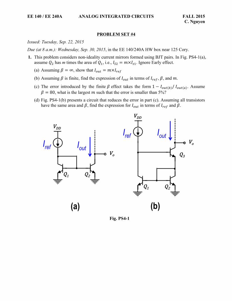
1. This problem considers non-ideality current mirrors formed using BJT pairs. In Fig. PS4-1(a), assume 𝑄! has m times the area of 𝑄!, i.e., 𝐼!! = 𝑚×𝐼!!. Ignore Early effect.
(a) Assuming 𝛽 = ∞, show that 𝐼!"# = 𝑚×𝐼!"#
(b) Assuming 𝛽 is finite, find the expression of 𝐼!"# in terms of 𝐼!"#, 𝛽, and 𝑚.
(c) The error introduced by the finite 𝛽 effect takes the form 1− 𝐼!"# ! / 𝐼!"# ! . Assume 𝛽 = 80, what is the largest 𝑚 such that the error is smaller than 5%?
(d) Fig. PS4-1(b) presents a circuit that reduces the error in part (c). Assuming all transistors have the same area and 𝛽, find the expression for 𝐼!"# in terms of 𝐼!"# and 𝛽.
Fig. PS4-1
Q2 Q1
VDD
Vo Iout Iref
Q2 Q1
Vo Iout Iref
VDD
Q3
(a) (b)
EE 140 / EE 240A ANALOG INTEGRATED CIRCUITS FALL 2015 C. Nguyen
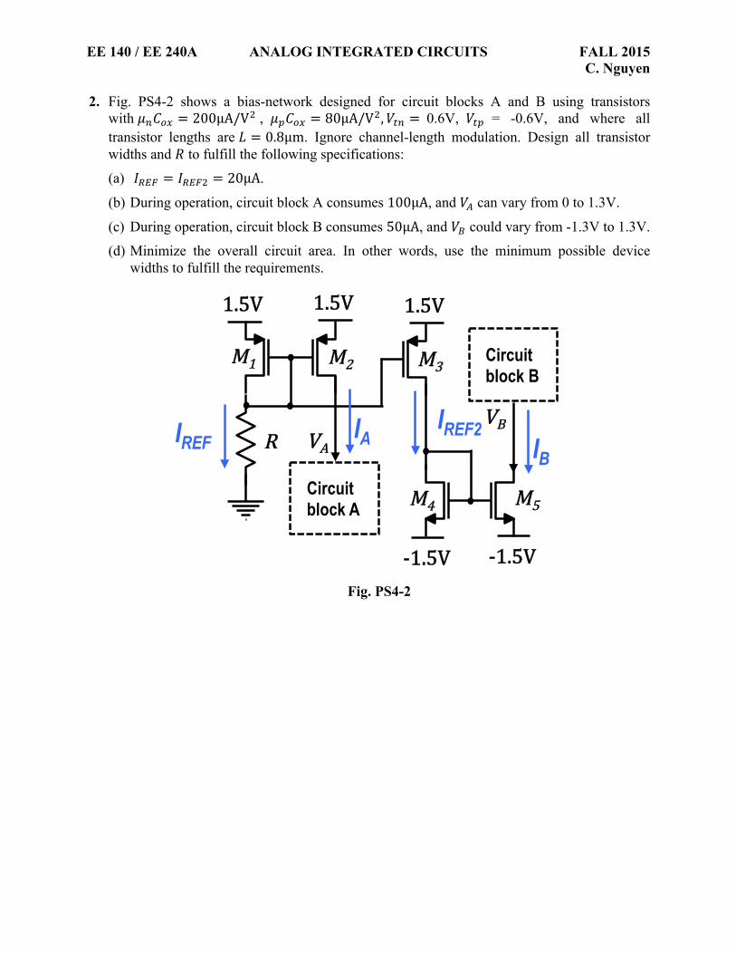
2. Fig. PS4-2 shows a bias-network designed for circuit blocks A and B using transistors
with 𝜇!𝐶!" = 200µμA/V! , 𝜇!𝐶!" = 80µμA/V!,𝑉!" = 0.6V, 𝑉!" = -0.6V, and where all transistor lengths are 𝐿 = 0.8µμm. Ignore channel-length modulation. Design all transistor widths and 𝑅 to fulfill the following specifications:
(a) 𝐼!"# = 𝐼!"#! = 20µμA.
(b) During operation, circuit block A consumes 100µμA, and 𝑉! can vary from 0 to 1.3V.
(c) During operation, circuit block B consumes 50µμA, and 𝑉! could vary from -1.3V to 1.3V.
(d) Minimize the overall circuit area. In other words, use the minimum possible device widths to fulfill the requirements.
Fig. PS4-2
M5
!1.5V
M4
!1.5V
1.5V 1.5V 1.5V
Circuit block A
Circuit block B
M2 M3 M1
IA IB IREF R
IREF2 VA VB

EE 140 / EE 240A ANALOG INTEGRATED CIRCUITS FALL 2015 C. Nguyen
3. For the transistors in the amplifier shown in Fig. PS4-3, 𝜇!𝐶!" = 800µμA/V! , 𝜇!𝐶!" =
400µμA/V!,𝑉!" = 0.8V, 𝑉!" = −0.8V, and 𝜆! = 𝜆! = 0.05V!!. The signal source 𝑉!"# is a small sinusoidal signal with no DC component.
(a) Neglecting channel-length modulation, design the value of 𝑉!"#$ such that the output swing is maximized.
(b) Find the midband voltage gain 𝑉!/𝑉!"#, 𝑅!", and 𝑅!"#.
(c) How large can 𝑉!"# swing (peak-to-peak) while 𝑀! and 𝑀! stay in saturation?
Fig. PS4-3
3.3V 3.3V
M2 M3
100µA
10µm
1µm
10µm
1µm
Vbias M1 5µm
1µm
Rs,=,50Ω
Vsig
Rin
Rout Vo

EE 140 / EE 240A ANALOG INTEGRATED CIRCUITS FALL 2015 C. Nguyen
4. Consider the BiCMOS amplifier shown in fig. PS4-4(a). The BJT has 𝑉!" = 0.7V, 𝛽 =200,
𝐶! = 0.8pF, and 𝑓! = 600MHz. The NMOS transistor has 𝑉! = 1V, 𝜇!𝐶!"𝑊/𝐿 = 2mA/V!, 𝐶!" = 2pF, and 𝐶!" = 1pF. The large feedback resistor 𝑅! helps with biasing, among other purposes. This problem considers the effect of 𝑅! .
(a) Find the dc bias current for 𝑀! and 𝑄!.
(b) Assuming 𝑅! = ∞, find the midband voltage gain 𝑉!/𝑉!"# , 𝑅!" , and 𝜔! of the circuit. You can neglect 𝐶!" and 𝐶!".
(c) Redo part (b) with 𝑅! = 10MΩ. Apply Miller theorem on 𝑅! . How does 𝑅! affect 𝑉!/𝑉!"#, 𝑅!", and 𝜔!?
(d) To mitigate the effect of 𝑅! one could cut 𝑅! into 2 segments and insert a large capacitor between them as in Fig. PS4-4(b). Redo part (c) with 𝑅! replaced with this new feedback network.
Fig. PS4-4
M1
Rs&=&7kΩ
RG&=&10MΩ
2V
Rsig&=&100kΩ
RC&=&3kΩ
RL&=&1kΩ ∞
∞Vsig
Rin
Q2
5V
Vo RG&=&10MΩ
RG1=&5MΩ RG2&=&5MΩ
∞
(a) (b)