a comparative study of electromagnetic dosimetric ... · temperature gain or from an electric...
TRANSCRIPT

Department of Electroscience
-
Master of Science Thesis Niklas Aronsson & Daniel Askeroth
April 2002
A Comparative Study ofElectromagnetic Dosimetric
Simulations and Measurements

1
Abstract In this master thesis a comparative evaluation between SEMCAD simulations and MapSAR measurements were made. SEMCAD is an electromagnetics simulation platform derived from the Finite Difference Time Domain method, FDTD. MapSAR is a measurements-tool for quick SAR assessment. Specific Absorption Rate, SAR, is a quantity expressing the amount of radiated power absorbed in a specific material. This is also the quantity in which health guidelines for Radio Frequency, RF, devices are set. The parameter used in this thesis was the maximum Peak SAR (i.e. not mass averaged SAR). SAR was the comparative quantity used since it is MapSAR’s primary readout and it is also a quantity that provides an easy comparison. A simplified cellular phone was used during this thesis, allowing a variety of test configurations and facilitating the import of the phone design into SEMCAD. The results of this thesis indicate that changes in SAR relative the reference phone-design’s SAR was coherent between simulations and measurements (for most cases). However, most changes in SAR are within the level of uncertainty, hindering a more explicit analysis of the results. Another cause for concern is that the absolute readings from the two systems differ by a factor two. In this thesis, this is compensated for by looking at relative changes to understand the impact of change in phone design.

2
Preface This master thesis was written during the winter 2001/2002 in Lund under the supervision of Daniel Sjöberg, PhD, at the Department of Electroscience. We would also like to thank Ramadan Plicanic, MScEE. for assistance during the DASY3-measurements. Other people deserving our gratitude are Kenneth Håkansson, MScEE for assisting us during the tedious soldering jobs and to André da Silva Frazão, MScEE, Thomas Bolin, MScAP&EE, for their revision of our thesis. For assisting us in the design of test cases Zhinong Ying, Licentiate has earned our appreciation. Lund March 2002 Niklas Aronsson & Daniel Askeroth
3
ABSTRACT ............................................................................................................................ 1
PREFACE ............................................................................................................................... 2
1 INTRODUCTION.................................................................................................................. 6
1.1 Background.......................................................................................................................................... 6
1.2 SAR-Specific Absorption Rate .......................................................................................................... 6
1.3 Depth of Penetration........................................................................................................................... 7
1.3 Antennas for Cellular Phones............................................................................................................ 8 1.3.1 The Patch Antenna....................................................................................................................... 10
1.4 Finite Difference Time Domain (FDTD), The Maxwell Equations ............................................. 10
1.5 Yee’s Algorithm................................................................................................................................. 12
1.6 Numerical Stability ........................................................................................................................... 12
1.7 Boundary Conditions........................................................................................................................ 13 1.7.1 Absorbing Boundary Conditions ................................................................................................. 13 1.7.2 Conducting Boundary Condition................................................................................................. 13 1.7.3 Periodic Boundary Condition ...................................................................................................... 14
1.8 Implementation ................................................................................................................................. 14
2. MEASUREMENTS AND SIMULATIONS........................................................................... 15
2.1 The Box Phone................................................................................................................................... 15
2.2 Antenna Matching Procedure.......................................................................................................... 16
2.3 Variations in the Box Phone Configuration................................................................................... 17 2.3.1 Reference Layout ......................................................................................................................... 17 2.3.2 Ground Positions.......................................................................................................................... 17 2.3.3 Resistors Layouts ......................................................................................................................... 17
2.4 MapSAR Measurement Equipment................................................................................................ 18 2.4.1 MapSAR Measurements .............................................................................................................. 18
2.5 SEMCAD Introduction .................................................................................................................... 19
3 RESULTS .......................................................................................................................... 20
3.1 70-µm Copper Tape Layer............................................................................................................... 20
3.2 4-µm Aluminium Layer.................................................................................................................... 22
3.3 Display Opening ................................................................................................................................ 23
3.4 Resistor Measurements .................................................................................................................... 24
3.5 Reliability of the Measurement Procedure .................................................................................... 25

4
4 DISCUSSION..................................................................................................................... 26
5. REFERENCES.................................................................................................................. 28
APPENDIX A: SOLIDS SPECIFICATIONS .......................................................................... 29
A.1 Box Phone Specifications................................................................................................................. 29
A.2 Antenna and Carrier Specifications............................................................................................... 29
A.3 Spherical Phantom........................................................................................................................... 29
A.4 Material Data.................................................................................................................................... 30
APPENDIX B: A SEMCAD PRIMER .................................................................................... 31
B.1 About.................................................................................................................................................. 31
B.2 Model Design with SEMCAD ......................................................................................................... 31
B.3 Sources and Sensors ......................................................................................................................... 32
B.4 Grid Settings ..................................................................................................................................... 34
B.5 Model Visualisation.......................................................................................................................... 37
B.6 Simulation Settings........................................................................................................................... 37
B.7 Starting a Simulation ....................................................................................................................... 40
B.8 Post-Processing ................................................................................................................................. 41
APPENDIX C MAPSAR MANUAL........................................................................................ 44
C.1 Introduction ...................................................................................................................................... 44
C.2 Description of the Graphical User Interface................................................................................. 44
C.3 Step by Step Measurements Guide for MapSAR ......................................................................... 47
APPENDIX D: MEASUREMENTS RESULTS ...................................................................... 48
D.1 Measurement Results....................................................................................................................... 48
D.2 Reference Designs: Near Field-Plots ............................................................................................. 49
D.3 Ground Positions: Near Field-Plots ............................................................................................... 50
D.4 Resistors: Near Field-Plots.............................................................................................................. 52
D.5 Ground Positions with Display: Near Field Plots......................................................................... 53
APPENDIX E: NUMERICAL RESULTS OF SEMCAD SIMULATIONS................................ 54
E.1 Perfect Conducting Front Layer .................................................................................................... 54

5
E.2 Perfect Conducting and Non Perfect Layers Comparison .......................................................... 54
E.3 Resistor Simulations without Display Opening ............................................................................ 54
E.4 Resistor Simulations with Display Opening .................................................................................. 54
E.5 No Front Layer ................................................................................................................................. 54
APPENDIX F: DASY3 MEASUREMENTS............................................................................ 55
F.1 DASY3 Results .................................................................................................................................. 55
F.2 DASY3 SAR Distribution Plots....................................................................................................... 55
APPENDIX G: ACRONYMS ................................................................................................. 58

6
1 Introduction Wire-less communication has become an important factor in everyday life for millions of people around the world. The widespread use of these radio frequency transmitters has made the safety concerns a hot topic and safety regulations have accordingly been set to limit the exposition. To help manufacturers comply with these safety standards it is vital to quickly assess the amount of radiation at any given stage of research and development without going through the hassle of certified testing. This thesis evaluates two different approaches, simulating antenna transmitters as well as using a simple small-scale workbench-measuring device. 1.1 Background The cellular phone market has increased substantially during the last decade. Along with market growth the possible risks related to the use of cellular phones have become an issue. As a measure of exposure to electromagnetic radiation SAR, Specific Absorption Rate, has been used. SAR translates to the loss in transmitted energy that is absorbed in human tissues, usually brain tissue. To meet with consumer demands concerning safety, standardisation institutes such as IEEE, Institute of Electrical and Electronics Engineers, and ICNIRP, International Commission on Non-Ionizing Radiation Protection, have set guidelines for the maximum SAR to enable a comparison between the various cellular phone manufacturers and models. The SAR value has now become mandatory for the manufacturers to be included with the phone. All new models have to meet with guidelines and legal restrictions so all phone models have to be tested. To prevent a phone prototype from having to be partially redesigned after failing to meet with maximum SAR regulations the ability to simulate or assess the maximum SAR at an early stage has become essential. SAR-simulations of a realistic cellular phone interacting with a head phantom are very computation-intensive. Therefore simulation tools capable of meaningful simulations such as SEMCAD have not been available until recently. The simulation programs are derivatives of numeric methods such as MoM, Method of Moment, FEM Finite Element Method, and FDTD, the Finite Difference Time Domain. FDTD has become the most common method due to its ability to work with complex problems over a wide range of frequencies. 1.2 SAR-Specific Absorption Rate SAR is a quantity that describes the amount of absorbed radiated effect for a specific material at a certain frequency. The quantity can be derived from either the temperature gain or from an electric field. The method used for measurements derives the radiated effect from the electric field since the difference in temperature is too small to measure in the cellular phone frequency band due to the low energies involved at these low frequencies (i.e. non-ionising radiation). SAR has become the most frequently used quantity involved when health issues are discussed. According to the ANSI/IEEE (American National Standard Institute/Institute of Electrical and
7
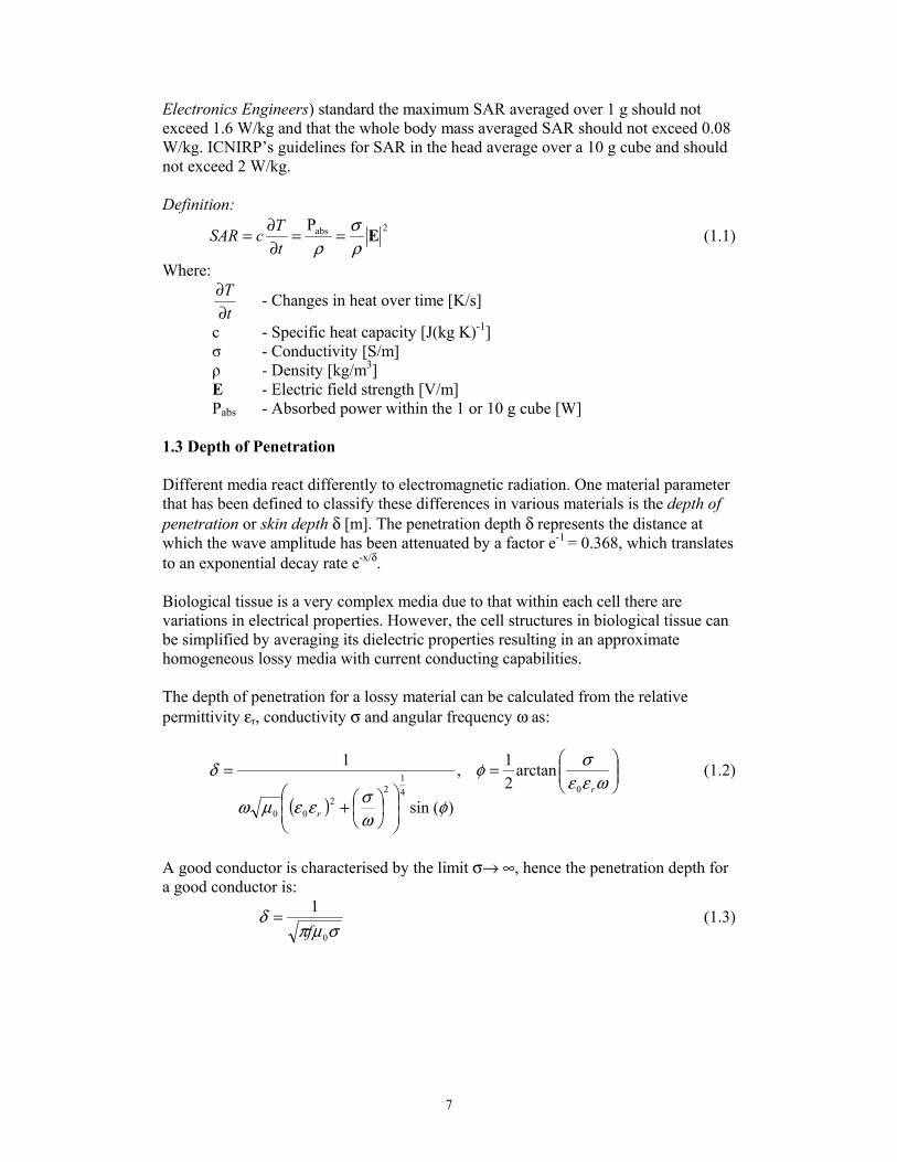
Electronics Engineers) standard the maximum SAR averaged over 1 g should not exceed 1.6 W/kg and that the whole body mass averaged SAR should not exceed 0.08 W/kg. ICNIRP’s guidelines for SAR in the head average over a 10 g cube and should not exceed 2 W/kg. Definition:
2absPE
ρσ
ρ==
∂∂=
tTcSAR (1.1)
Where:
tT
∂∂ - Changes in heat over time [K/s]
c - Specific heat capacity [J(kg K)-1] σ - Conductivity [S/m] ρ - Density [kg/m3]
E - Electric field strength [V/m] Pabs - Absorbed power within the 1 or 10 g cube [W] 1.3 Depth of Penetration Different media react differently to electromagnetic radiation. One material parameter that has been defined to classify these differences in various materials is the depth of penetration or skin depth δ [m]. The penetration depth δ represents the distance at which the wave amplitude has been attenuated by a factor e-1 = 0.368, which translates to an exponential decay rate e-x/δ. Biological tissue is a very complex media due to that within each cell there are variations in electrical properties. However, the cell structures in biological tissue can be simplified by averaging its dielectric properties resulting in an approximate homogeneous lossy media with current conducting capabilities. The depth of penetration for a lossy material can be calculated from the relative permittivity εr, conductivity σ and angular frequency ω as:
( )
=
+
=ωεε
σφ
φωσεεµω
δr
r
041
22
00
arctan21,
)(sin
1 (1.2)
A good conductor is characterised by the limit σ→ ∞, hence the penetration depth for a good conductor is:
σµπδ
0
1f
= (1.3)

8
Conductor (copper) Brain tissue (homogenous)Angular Frequency ω [rad/s] 2π900×106 2π900×106 Permittivity ε0 [F/m] (36π)-1×10⁻⁹ (36π)-1×10⁻⁹ Relative Permittivity εr 1 42 Permeability µ0 [H/m] 4π×107 4π×107 Conductivity σ [S/m] 5.8×10⁷ 1.1 Attenuation Constant α [m-1] 4.54×10⁵ 31.0 Depth of Penetration δ [m] 2.0×10⁻⁶ 3.2×10⁻² Table 1.1 A comparison between conductor and a lossy material at 900 MHz As seen in the comparison in Table 1.1, the attenuation is very large in a good conductor, which makes it well suited to block undesired radiation. For more information on penetration depth in lossy media see [6] and [8]. 1.3 Antennas for Cellular Phones An antenna is a transmitting and/or receiving instrument for electromagnetic communication. The antenna can be approached from two directions, either as a radiator in free space or as an electrical component in an electrical circuit. Every antenna has a specific radiation pattern describing its field properties. The radiation pattern is defined “as a mathematical function or a graphical representation of the radiation properties of the antenna as a function of space coordinates. In most cases, the radiation pattern is determined in the far-field region and is represented as a function of the directional coordinates. Radiation properties include power flux density, radiation intensity, field strength, directivity, phase or polarization.“[1, p.28]
Figure 1.1 Spherical Coordinates Antenna performance parameters such as gain and directivity can be derived from the far-field radiation pattern. These two parameters are closely related where the relative gain parameter is defined as “the ratio of the power gain in a given direction to the power gain of a reference antenna in its referenced direction.”[1, p.58] The directivity is "the ratio of the radiation intensity in a given direction from the antenna to the radiation intensity averaged over all directions.”[1, p.39]

9
∞≤≤ SWR1
0,log20 1111 ≤<∞−Γ= SS
1→Γ⇒∞→SWR
When describing the antenna as an electrical component the voltage reflection coefficient Γ is defined as the ratio of the complex amplitudes of the reflected and incident voltage waves at the load. For passive components the reflection coefficient satisfies 1≤Γ and can be calculated as:
ZL - load impedance and Z0 - characteristic impedance (1.4)
From the voltage return coefficient another interesting parameter can be derived. The Standing Wave Ratio, SWR or Voltage SWR as it is also known, is defined as:
(1.5)
The standing wave ratio is a very good measure to determine whether the antenna is correctly matched to the desired frequency and whether it meets with the desired bandwidth. In the extreme cases with SWR=1 all the power is transmitted and the other extreme can be interpreted as if none of the power was transmitted to the antenna since:
(1.6)
Analogously with the SWR the Return Loss S11 can be derived from the voltage return coefficient. S11 is defined as the return loss from the transmitter and back.
(1.7)
The S11 parameter displays the amount of power reflected at a specific frequency. Both the return loss and the standing wave ratio are two different visualisations of the same parameters representing the resonance frequency and the return-damping factor, see Figures 1.2 and 1.3.
Figure 1.2 Figure 1.3 Standing Wave Ratio (single band) Return Loss S11 (dual band) The most common types of cellular phone antennas used today are retractable (telescope), helical and internal (patch) antennas, but since this thesis only concern the patch antenna the others will be excluded from further presentation.
0
0ZZZZ
L
L+−
=Γ
Γ−Γ+
==11
min
maxEE
SWR

10
1.3.1 The Patch Antenna Patch antennas in cellular phones are internal antennas. The patch antenna is a thin metal sheet etched on a dielectric carrier structure. The metal patch plane is parallel to the ground plane, see Figure 1.4. The metal patch can take on various shapes such as circular, rectangular or irregular. Another important parameter is the feed point that has to be considered since it plays a significant role to the characteristic impedance. The antenna feed structure might differ, but usually the patch is fed from a pogo pin (a spring-mounted conductor) or a micro strip.
Figure 1.4. The Single-band Patch Antenna Simplified half-wave patch parameters from Figure 1.4 can be calculated, however since these parameters will be altered due to reflections from the cellular phone cover and to changes in load parameters no effort has been made to do so. The antenna feed placement will also alter the results, so to optimise the antenna performance the whole phone model has to be tested. For more information concerning antennas see [4] and [11]. 1.4 Finite Difference Time Domain (FDTD), The Maxwell Equations Electromagnetics is the study of electric charges or in this case electric fields, i.e. spatial distributions. There are three ways to predict electromagnetic fields and their effects on different materials; by experiment, analysis or computation. Most problems have the complexity to make a theoretical analysis impossible and experimentation can be prohibitively costly and time consuming. Several numerical methods are today available for electromagnetic computational analysis like Methods of Moments (MoM), Finite Element Method (FEM) and Finite Difference Time Domain (FDTD). These applications have become more and more useful with the increasing accessibility of computer power that the last decades have brought. FDTD is well suited for calculating transients as well as single frequencies or continuous wave sources.

11
The Maxwell equations describe the electromagnetic field behaviour completely as long as the data, such as the material properties and initial conditions, are known. In equation 1.14-17 the Maxwell equations are presented in their differential form.
t∂∂−=×∇ BE Faraday’s law of electromagnetic induction (1.14)
t∂∂+=×∇ DJH Ampère’s circuital law (1.15)
0=•∇ B (1.16)
ρ=•∇ D Gauss’s law (1.17)
The four Maxwell equations are not independent since 1.16-17 can be derived from 1.14-15 using the equation of continuity (
t∂∂−=•∇ ρJ ). In order to solve equations
1.14-15 the following two constitutive equations are needed, which describe the material’s behaviour.
ED ε= Where 0εεε r= (1.18) HB µ= Where 0µµµ r= (1.19)
The symbols used above are defined and known as the following quantities. B is the magnetic flux density [Vs/m2 or Tesla] D is the electric displacement [As/ m2] E is the electric field intensity [V/m] H is the magnetic field Intensity [A/m] J is the current density [A/m2] The permittivity ε0 [As/Vm] is for free space whereas εr is the relative permittivity, and is dependent on the material in question, which can also be said for the permeability µ [Vs/Am]. For free space the permeability is µ0 and µr has material dependencies. All relative constants are dimensionless by definition. If the E-field is discretised in space and time with a uniform step and only field values at these points are stored, this can be written as equation 1.20.
),,,(,,
tnzkyjxiEE n
kji∆∆∆∆= (1.20)
Using the terminology below one can substitute derivatives with an approximate difference. Equation 1.21 shows the finite difference formula for the first derivative.
t
EE
tt
EEE
nkji
nkji
tkji
tkji
t tt ∆
−≈
−
−=∂
−+
→− 2
1,,
1,,
12
,,,,12
012lim (1.21)

12
1.5 Yee’s Algorithm Yee penned his algorithm in 1966 [9], since then extensive research have expanded and enhanced the original idea and applied it to a wide range of problems. The recent upswing in its popularity is undoubtedly thanks to the decreasing cost of computer calculations. The Yee algorithm uses a numerical solution to Maxwell’s curl equations using a discretised differential form. The big novelty in Yee’s algorithm was his grid definition that greatly decreased the amount of memory required. The E-field is defined on one grid and the H-field on another in the time domain. Both grids are offset in time and space. Each field is updated with a leapfrog scheme and a finite difference form of the curl using the values of the surrounding cells. The electric field is solved at one moment in time and then the magnetic field is solved at the next moment (half a time step) similar to the game, leapfrog. This is repeated until the simulation is done. For a general presentation of the FDTD method and Yee’s algorithm, see [5] and [7].
Figure 1.5 The Yee Cell 1.6 Numerical Stability To ensure a stable and converging solution the cell size and time step must be wisely chosen. Choosing a grid too fine the simulation will be penalised with an unnecessary long computational time and in most cases not result in increased accuracy. It is clear that the cell size should be shorter than the wavelength of interest. The cell size suggested by the Nyquist theorem (i.e. two samples per wavelength) will normally not suffice due to the approximate nature of FDTD computation. A more realistic cell size would be somewhere between 1/10 and 1/20 of the wavelength. It is possible to use non-uniform cells with a finer cell size (grid) near complex areas, although these areas may have to be interpolated both in time and/or space with the rest of the grid. For solids with penetrable materials the wavelength is shorter inside these for a given frequency thus requiring a smaller cell size. Cells also have to be small enough to give an accurate model of the actual geometry. Rounded objects will suffer from the “staircase” effect when modelling them with rectangular cells, i.e. the problem of building circles and other non-rectangular objects with cubes.

13
After the cell size has been set, next step is to determine a suitable time step ∆t. The Courant-Friedrich-Levy criterium sets the limit for a stable solution (Figure 1.26).
222 )(1
)(1
)(1
1
zyxc
t
∆+
∆+
∆
≤∆ Courant-Friedrich-Levy criterium (1.26)
Here ∆x, ∆y and ∆z are the mesh size for the smallest cell to be found globally in the grid for each axis. The parameter c is the speed of light within the cell material. The rule of thumb is that a propagating wave must not travel through more than one cell in one time step. Larger time steps than the one given with the above condition will quickly result in instability. 1.7 Boundary Conditions Antenna models using FDTD are usually located in free space making a boundary condition necessary to make sure that the reflected fields do not bounce back into the computation space, since a infinite computational volume is impossible. Using an Outer Radiation Boundary Condition (ORBC) to absorb incoming fields at the outer limits is the only solution, otherwise the calculations have to be aborted when the reflected wave reaches the outer computational limit. Also since the outer co-ordinates cannot be updated using the normal finite difference equations an ORBC is needed for simulations. Several types of boundary approximations are available to enclose the computational space. SEMCAD offers the three types of Boundary Conditions described in the following paragraphs [2].
1.7.1 Absorbing Boundary Conditions Absorbing Boundary Conditions (ABC) simulates materials that absorbs outgoing waves or free space conditions. Ideally they should allow any outgoing wave to exit without any reflection. A popular technique that can be described as a material absorber is the Perfectly Matched Layer technique (PML). This has been shown to be one of the most accurate algorithms. Other ABC’s that SEMCAD has implemented are the first and second order Mur and the Higdon operator (up to the 4th order) that offers better performance than PML but may be not as numerically exact.
1.7.2 Conducting Boundary Condition The Conducting Boundary Condition (CBC) does simply what the name suggests. The computational space is truncated with a perfectly conducting plane that can be perfect electrically (PEC) or magnetically conducting (PMC). Incoming tangential E- or H-fields components are set to zero.

14
1.7.3 Periodic Boundary Condition Periodic Boundary Condition can simulate periodic boundaries. Values from the other side of the grid are used for periodic computation. 1.8 Implementation A FDTD simulation basically contains three steps. First the grid must be built and defined and the initial conditions set. The number of cells in each dimension must be determined as well as the size of each cell and the electrical properties of each cell. Other specifications necessary are where and what to be monitored and for how many time steps the computation shall proceed. After the time step has been set according to the smallest cell size using the Courant-Friedrich-Levy criterion the fields can be updated. After the initial specifications are set, the second part can commence. This is the heart of the simulation where the field is advanced step after step. When the criteria for terminating the simulation have been fulfilled the final part of a FDTD simulation can begin, the post processing. This is where the calculated data is processed and then presented in any manner desired by the user.

15
2. Measurements and Simulations To make an evaluation of the MapSAR and the SEMCAD utilities possible a suitable comparison quantity had to be selected. For this thesis SAR was chosen since it is the best presented output from MapSAR. Different comparison scenarios were designed to alter the near field, aiming at making the results significant. This chapter is intended to clarify the methods and scenarios used. 2.1 The Box Phone For this master thesis a simplified cellular phone was used, referred to as the Box phone from here on. The reason for using a simplified phone design is to minimise the number of cells needed during simulations in SEMCAD, thereby minimising the number of simplifications needed for the simulated model. Another concern for the simplified model was doubts about SEMCAD’s ability to simulate complex models, like a faithful representation of a real phone, and simply because it facilitates changes in the phone. The box phone is made of plastic materials, see Figure 2.1. For further details see Appendix A. It transmits with an internal dual band antenna (PIFA) fitted on a plastic carrier mounted on the antenna ground plane. Several fronts, each with different conductive layers, were tested with the phone. Different scenarios for interaction with these front layers will be discussed further on.
Figure 2.1 The Box Phone The simulated Box phone differs geometrically from the actual one in two major aspects, it has no battery and no opening around the battery to allow an on/off switch. Other minor differences are that the simulated phone lacks assorted details such as screws and bolts to fit the antenna carrier onto the ground plane, the PCB.
16
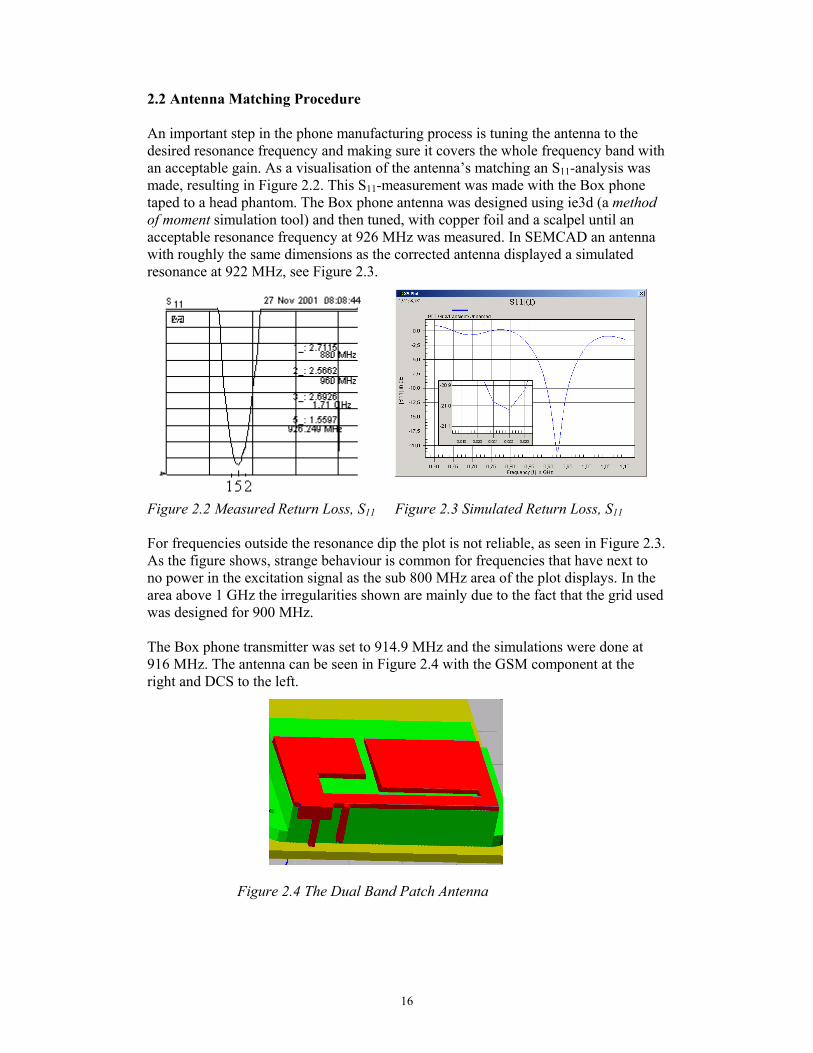
2.2 Antenna Matching Procedure An important step in the phone manufacturing process is tuning the antenna to the desired resonance frequency and making sure it covers the whole frequency band with an acceptable gain. As a visualisation of the antenna’s matching an S11-analysis was made, resulting in Figure 2.2. This S11-measurement was made with the Box phone taped to a head phantom. The Box phone antenna was designed using ie3d (a method of moment simulation tool) and then tuned, with copper foil and a scalpel until an acceptable resonance frequency at 926 MHz was measured. In SEMCAD an antenna with roughly the same dimensions as the corrected antenna displayed a simulated resonance at 922 MHz, see Figure 2.3.
Figure 2.2 Measured Return Loss, S11 Figure 2.3 Simulated Return Loss, S11 For frequencies outside the resonance dip the plot is not reliable, as seen in Figure 2.3. As the figure shows, strange behaviour is common for frequencies that have next to no power in the excitation signal as the sub 800 MHz area of the plot displays. In the area above 1 GHz the irregularities shown are mainly due to the fact that the grid used was designed for 900 MHz. The Box phone transmitter was set to 914.9 MHz and the simulations were done at 916 MHz. The antenna can be seen in Figure 2.4 with the GSM component at the right and DCS to the left.
Figure 2.4 The Dual Band Patch Antenna

17
2.3 Variations in the Box Phone Configuration To test SEMCAD’s ability to simulate complex models, different scenarios aiming to alter the electromagnetic characteristics of the Box phone were evaluated. These approaches involve alterations in the conductive shield and ground positions.
2.3.1 Reference Layout Figure 2.5 shows the standard front layouts used. These will later be used as the basis of both measurements and simulations for the schemes discussed in the following paragraphs.
a.) No conductive shield b.) 4 or 70-µm thick conductive shield c.) Display opening and a 2-mm gap d.) Display opening with a conductive
display patch and a 2-mm gap
Figure 2.5 Reference Layout
2.3.2 Ground Positions All ground positions used are accounted for in Figure 2.6. Two different materials were used for the front layers, a 70-µm thick copper-tape and a 4-µm thick layer of aluminium.
Figure 2.6 Ground Positions
2.3.3 Resistors Layouts An interesting feature for this thesis available in the SEMCAD simulation platform is electromagnetic models of electric circuits, such as resistors, capacitors and inductors. To test SEMCAD’s ability to handle this feature two rather basic schemes using a resistor at the centre of the phone over a 2-mm gap as well as two resistors parallel at each side over the same gap. These layouts can be seen in Figure 2.7.

18
a.) Single resistor, either 5 or 10 Ω. b.) Two resistors parallel, each 10 or 20 Ω. c.) As b.) with display patch
Figure 2.7 Resistor Configuration 2.4 MapSAR Measurement Equipment SAR measurements were performed with MapSAR benchtop SAR assessment equipment, Figure 2.8, developed by Index SAR. It consists of a spherical phantom, an E-field probe with amplifier and a data converter. For the placement of the phone there is also positioning-rack, allowing movements in all directions, with a partial rotation, constructed in plastics to counteract reflections. All SAR readings measured with the MapSAR system in this thesis are not averaged over mass. Non-averaged readings from MapSAR are calculated from measured E-fields in the liquid.
Figure 2.8 The MapSAR Equipment The probe movement is restricted to spherical coordinates with a fixed radius and origin of coordinates in the centre of the spherical phantom. A plastic arm is mounted on the sphere to render tracing of the probe movements through a drawing board. The drawing board has an underlay with a pattern suggesting the probe-movement. Using coordinates from the drawing board, the MapSAR software can determine the probe position. The software keeps track of the maximum SAR and plots a 2D graph of the SAR where each point is displayed on top of an imported image of the phone model.
2.4.1 MapSAR Measurements Before starting a measurement the E-field probe is positioned at the start position; Figures 2.9-10 in the probe’s horizontally suspended position. The object that is to be measured is positioned in the phone holder touching the sphere.
Figure 2.9 Figure 2.10 “Start-position” from a lateral view “Start-position” from the top view

19
The measurement procedure basically consists of six steps: i.) Placing the probe in the start position relative the phone (Figures. 2.9 & 2.10). ii.) Taking an initial SAR-reading at the start position for comparison with (v.). iii.) Scanning the phone surface using the mask design on the Wacom-board as a
reference. iv.) Scanning extensively around the maximum SAR position(s) to determine the
absolute maximum. v.) Comparing the final SAR-reading at the start position to the initial (ii.) to
determine the drift i.e. changes in SAR-reading. vi.) Noting the maximum SAR-readout. The readings can be exported as raw data (text file) with coordinates, phone outline and conductivity for further analysis and the 2D plot produced in the main window can be saved as a windows bitmap file. To minimise errors the measurements for each phone configuration were made twenty times to avoid aberrations due to phone position and to minimise other possible sources of uncertainty. Another possible source of uncertainty could be differences in batteries; to be able to distinguish battery problems in the results two batteries with similar properties were selected and then replaced every ten measurements. For a more extensive guide to the MapSAR benchtop SAR assessment equipment see Appendix C. 2.5 SEMCAD Introduction SEMCAD is an electromagnetics simulation platform using a FDTD solver. It is very well suited for simulating antenna designs, dosimetry, electromagnetic interference (EMI)/ electromagnetic compatibility (EMC) and optics involving complex objects. SEMCAD (the Simulation platform for EMC, Antenna Design and Dosimetry) is developed by Schmid & Partner Engineering AG (SPEAG) in conjunction with several Swiss universities. It offers a graphical user interface for computer-aided design called ACIS made by Spatial coupled with SPEAG’s FDTD implementation for a slick user-friendly interface. Please refer to Appendix B and the SEMCAD Reference Manual [2] for information on how to set up and run simulations.

20
3 Results 3.1 70-µm Copper Tape Layer Copper tape (70-µm thick) was put on the inside of the front piece. A short piece of conducting elastomer (conductive rubber) was used to ground the copper tape on the front with the main board holding the carrier as well as the circuit board. The objective here is to see how placing a ground at various positions interacts with the copper layer. For maximum convenience the different ground positions is listed again in Figure 3.1.
Figure 3.1 Ground Positions Ground positions C, D and E1+E2 are the only ones showing a significant SAR deviation compared to the case with floating copper layer according to the MapSAR measurements with respect to the margins of error. As Figure 3.2 shows, the highest SAR value comes with grounding at position C and the lowest values with grounding at E1+E2. SAR is decreased by almost 40 % comparing those two values.
0.460.46
0.430.47
0.430.53
0.370.42
0.450.33
0.450.46
0.42
0 0.1 0.2 0.3 0.4 0.5 0.6
Floating
A
B1
B2
B1 + B2
C
D
E1
E2
E1 + E2
F1
F2
F1 + F2
SAR (W/Kg)
Figure 3.2 Measured SAR Values with 70-µm Copper Layer for Various Ground Positions
21
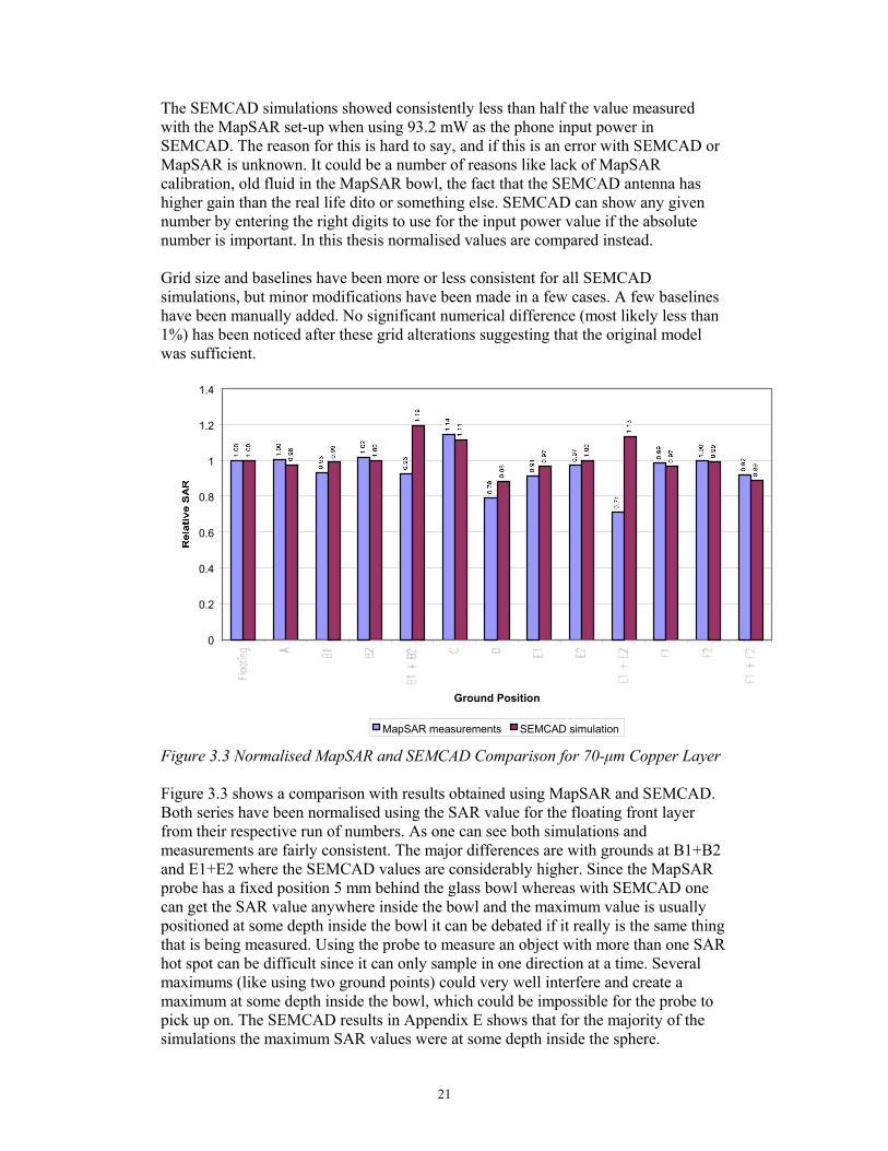
The SEMCAD simulations showed consistently less than half the value measured with the MapSAR set-up when using 93.2 mW as the phone input power in SEMCAD. The reason for this is hard to say, and if this is an error with SEMCAD or MapSAR is unknown. It could be a number of reasons like lack of MapSAR calibration, old fluid in the MapSAR bowl, the fact that the SEMCAD antenna has higher gain than the real life dito or something else. SEMCAD can show any given number by entering the right digits to use for the input power value if the absolute number is important. In this thesis normalised values are compared instead. Grid size and baselines have been more or less consistent for all SEMCAD simulations, but minor modifications have been made in a few cases. A few baselines have been manually added. No significant numerical difference (most likely less than 1%) has been noticed after these grid alterations suggesting that the original model was sufficient.
0
0.2
0.4
0.6
0.8
1
1.2
1.4
Ground Position
MapSAR measurements SEMCAD simulation
Figure 3.3 Normalised MapSAR and SEMCAD Comparison for 70-µm Copper Layer Figure 3.3 shows a comparison with results obtained using MapSAR and SEMCAD. Both series have been normalised using the SAR value for the floating front layer from their respective run of numbers. As one can see both simulations and measurements are fairly consistent. The major differences are with grounds at B1+B2 and E1+E2 where the SEMCAD values are considerably higher. Since the MapSAR probe has a fixed position 5 mm behind the glass bowl whereas with SEMCAD one can get the SAR value anywhere inside the bowl and the maximum value is usually positioned at some depth inside the bowl it can be debated if it really is the same thing that is being measured. Using the probe to measure an object with more than one SAR hot spot can be difficult since it can only sample in one direction at a time. Several maximums (like using two ground points) could very well interfere and create a maximum at some depth inside the bowl, which could be impossible for the probe to pick up on. The SEMCAD results in Appendix E shows that for the majority of the simulations the maximum SAR values were at some depth inside the sphere.
22
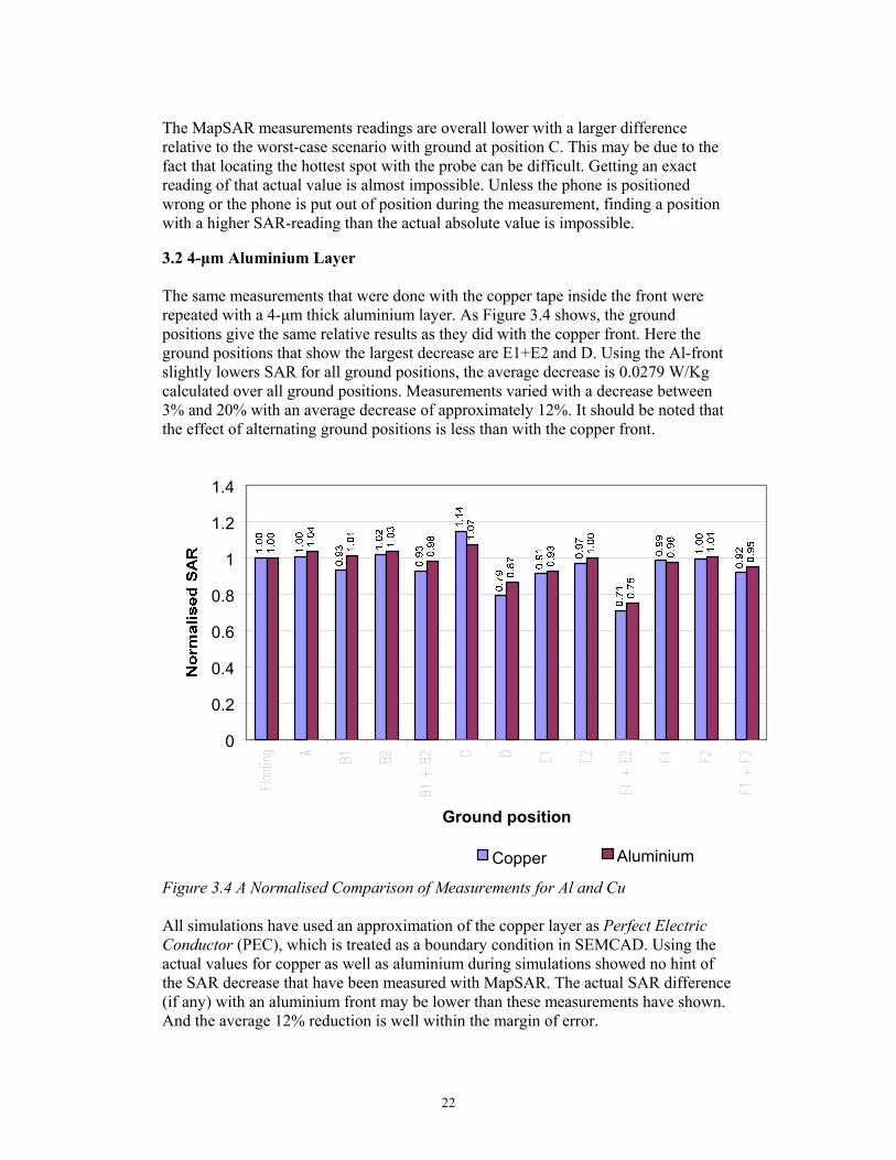
The MapSAR measurements readings are overall lower with a larger difference relative to the worst-case scenario with ground at position C. This may be due to the fact that locating the hottest spot with the probe can be difficult. Getting an exact reading of that actual value is almost impossible. Unless the phone is positioned wrong or the phone is put out of position during the measurement, finding a position with a higher SAR-reading than the actual absolute value is impossible. 3.2 4-µm Aluminium Layer The same measurements that were done with the copper tape inside the front were repeated with a 4-µm thick aluminium layer. As Figure 3.4 shows, the ground positions give the same relative results as they did with the copper front. Here the ground positions that show the largest decrease are E1+E2 and D. Using the Al-front slightly lowers SAR for all ground positions, the average decrease is 0.0279 W/Kg calculated over all ground positions. Measurements varied with a decrease between 3% and 20% with an average decrease of approximately 12%. It should be noted that the effect of alternating ground positions is less than with the copper front.
0
0.2
0.4
0.6
0.8
1
1.2
1.4
Ground position
Copper AluminumAluminium
Figure 3.4 A Normalised Comparison of Measurements for Al and Cu All simulations have used an approximation of the copper layer as Perfect Electric Conductor (PEC), which is treated as a boundary condition in SEMCAD. Using the actual values for copper as well as aluminium during simulations showed no hint of the SAR decrease that have been measured with MapSAR. The actual SAR difference (if any) with an aluminium front may be lower than these measurements have shown. And the average 12% reduction is well within the margin of error.

23
As a comparison between copper and aluminium fronts, measurements with no ground position for each case were made on a DASY3-system. For more information regarding the DASY3 system see [3]. Just as in SEMCAD and MapSAR the difference between copper and aluminium fronts was minimal and well within the margin of error. The DASY3 showed a 7% higher reading for aluminium than for copper. These measurements were performed for the left cheek position. 3.3 Display Opening Measurements were done using the copper tape but with a rectangular opening where a display normally would be positioned. As earlier the effects of using a ground between the PCB and the copper front was investigated. There was some interesting resonance with ground positions D and E1+E2 as can be seen in Figure 3.5. Both SEMCAD and MapSAR readings shows the same behaviour but with a greater resonance shown with MapSAR. This may be due to the small differences in the position and size of the display opening between the actual phone and our SEMCAD model. For the non-resonant ground positions the results were very close.
0
1
2
3
4
5
6
Floating B1+B2 D E1+E2 F1+F2
Ground Position
MapSAR (Normalised with floating) SEMCAD (Normalised with floating)
Figure 3.5 SAR Comparison with Display Opening

24
3.4 Resistor Measurements For this measurement series the copper layer was separated by a 2 mm gap. The upper half of the copper layer still had the display opening. Resistors were soldered to the front to join the two parts in different configurations. All resistor configurations can be seen in Figure 3.6.
Figure 3.6 Measurement Cases Using Resistors Case 1: A single 10 Ω resistor. Case 2: Two 20 Ω resistors parallel at each side. Case 3: A single 5 Ω resistor in the centre. Case 4: Two 10 Ω resistors parallel at each side. Case 5: As Case 2 with floating display patch. Case 6: No resistors. As Figure 3.7 shows the results were somewhat similar. Simulations showed no major numerical difference for the different cases and the measurements suggest the same tendency with one exception. Measured values for Case 1 is somewhat higher than simulated.
1,11
0,87
1,02
0,89
0,89
1,00
0,91
0,90 0,
95
0,90 0,93 1,
00
0,0000
0,2000
0,4000
0,6000
0,8000
1,0000
1,2000
Case 1 Case 2 Case 3 Case 4 Case 5 Case 6
Nor
mal
ised
SA
R
Measured Simulated
Figure 3.7 Simulation and Measurement Comparison with Resistors

25
3.5 Reliability of the Measurement Procedure To examine the reliability of the MapSAR measurements a statistical survey of the results were made. The reliability of the SAR-measurements had a maximum deviation of between 4% and 10.5% for 20 measurements including one battery change on the same phone configuration. The standard deviation ranged between 2% and 6%, see Appendix D. Another factor of uncertainty is the antenna mismatch, which might result in up to 15% bias. The mismatch factor of the antenna was derived via a comparison between the Gain parameter for SWR 2 and 3. A set of light emitting diodes show how well matched the phone is at any given moment, all measurements showed a SWR between 2 and 3. To determine the gain more precisely than this is not possible without tests and it is this uncertainty that the before mentioned 15% comes from. The antenna mismatch is the result of changes in the impedance due to modifications of the phone. The worst-case scenario adds up to a 25.5% deviation between two single measurements.

26
4 Discussion One thing that became clear during this thesis is that some tools are better suited than others for a given task. First of all the MapSAR system has a very small measurement area due to the spherical shape of the phantom. The spot on the phone with the maximum SAR should be positioned next to the probe’s resting position. Accredited testing uses a head and shoulder SAM phantom, approximating a head phantom with a sphere instead takes some consideration. For measurement positions with a tilted phone, some phone shapes gives two touch positions (i.e. where the phone is touching the SAM phantom). With a ground position that moves the peak SAR to the lower part of the phone, a MapSAR reading measuring the top of the phone will show a reduced SAR readout. A DASY3 reading where the lower part of the phone is right next to the cheek as well as the ear will not display the same value as the MapSAR where the probe is at a greater distance from the more transmitting part of the phone. The DASY3 probe will get much closer to the lower part of the phone as well and pick up a ‘normal’ value. The MapSAR system should thus only be used for measurement around the maximum value, i.e. the area with the hotspot should be positioned next to the probe to make up for the differences between a spherical bowl and a head SAM where a larger area of the phone will be close to the SAM. This can be seen as worst-case scenario measurements, finding the maximum SAR anywhere on the phone regardless of its position and if it can be measured with a SAM phantom. SEMCAD simulations are ideal for visualising hotspots. Using the simulation post-processing is a good basis for MapSAR measurements since the user can easily determine the locations likely to show a high SAR in reality as well. However using MapSAR to find the location of maximum SAR on a phone surface can be done fairly quickly and to later use that position for a more thorough measurement of the absolute value as reference. The strength of the MapSAR is the short measurement time, which makes it ideal for comparative tests. This is one of the biggest selling arguments of the MapSAR system. Another benefit it has over a complex robotic set-up is that the liquid is sealed which gives it a longer life. Also since each measurement takes 2-3 minutes at the most it is less likely that the batteries will drain during a measurement or that the characteristics of the measured object will change due to overheating. SEMCAD is a very useful tool when it comes to getting an idea of how complex structures such as models of cellular phones will interact with surrounding structures. Seemingly identical antenna geometrical dimensions in SEMCAD as the real world original design did result in slightly different antenna characteristics. Maybe the SEMCAD model requires a more detailed representation (like a cad file of the actual phone). The real antenna was cut out by hand and messed up with the soldering iron, which makes it impossible to model down to a certain degree of accuracy. Another difference is to which extent the electric properties given to solids in the SEMCAD simulations are accurate. While the differences in antenna performance may not be significant it may lead to somewhat different absolute numerical results but should be of no concern for relative comparisons between different simulation scenarios. Using SEMCAD as a serious

27
development tool requires a fast computer, the faster the more realistic and rewarding simulations are possible. MapSAR usually reported a SAR value twice as high as the SEMCAD simulations. This may be due to the differences in antenna gain or perhaps the fact that the measured power from the phone had been measured without the mismatch that were present during all measurements. Due to the fact that MapSAR is designed for averaged measurements (the probe’s position was set with this in mind) it may not be ideal to compare peak SAR. The MapSAR set up requires a corrective factor for comparisons with DASY3 measurements due to its 4mm thick bowl whereas SAM phantoms often use a 2mm thick shell. An uncorrected MapSAR value will thus be lower than a DASY3 reading. With careful calibration some MapSAR measurements could be fairly accurate, if the procedure is done carefully, and the differences between a spherical and a SAM phantom are kept in mind. This causes some practical issues regarding where on the test object measurements shall be done as discussed earlier. Using a complex head phantom in SEMCAD is very feasible. It is not a very big part of the head that interacts with the phone especially with the depth of penetration in mind. Figure 4.1 shows how the complex shape of a SAM phantom is approximated in a SEMCAD simulation. There is no real loss in accuracy with a more crude head approximation, as shown in the picture to the right below, so the choice of tissue for SAR extraction should be made with respect to whatever measurement method one aims to simulate. With an efficient grid design using a head phantom must not imply more cells than a spherical phantom (Figure 4.2).
Figure 4.1 Head Phantom Figure 4.2 Spherical Phantom Both SEMCAD simulation and MapSAR simulations are fine tools for relative studies of antennas. As seen in chapter 3 the normalised results show the same tendencies for each test scenario with a few exceptions. The only really useful SAR measurement is done on accredited systems like the DASY3 but it should be possible with reference measurements from an accredited system to predict the actual value from results using SEMCAD and/or MapSAR. MapSAR with its spherical phantom makes it less versatile than SEMCAD and harder to compare with results using a head phantom.
28
5. References
[1.] Balanis, A. C., “Antenna Theory: Analysis and Design”, 2nd edition, John Wiley & Sons Inc. 1997
[2.] “SEMCAD Reference Manual”. Bundled with SEMCAD and available at: http://www.semcad.com/downloads_free/SEMCAD_RefManual.pdf
[3.] http://www.speag.com [4.] Fujimoto, K. and James, J. R., ”Mobile Antenna Systems Handbook”, 2nd edition, Artech
House Publishers, 2001 [5.] Kunz, K. S., and Luebbers, R. J., “The Finite Difference Time Domain Method for
Electromagnetics”, CRC Press 1999 [6.] Cheng, D. K., “Field and Wave Electromagnetics”. 2nd edition, Addison-Wesley 1989 [7.] A. Taflove. “Computational electrodynamics: The Finite-Difference Time-Domain
Method”. Artech House, Boston, London, 1995. [8.] C. Gabriel, S. Gabriel and E. Corthout, “The dielectric properties of biological tissues: 1-3”,
Phys. Med. Biol. 41, 1996. pp. 2232-2293. [9.] K.S Yee. Numerical Solution of initial boundary problems involving Maxwell’s equations
in isotropic media. IEEE Trans. Antennas Propagat.,14. March 1966. [10.] “Indexsar, Mapsar Sytem Manual”. 2001 [11.] Stutzman, W. L. and Thiele, G. A., “Antenna Theory and Design”, 2nd edition, John Wiley
& Sons Inc. 1998 [12.] ”SEMCAD Tutorial”. Bundled with SEMCAD and available at:
http://www.semcad.com/downloads_free/SEMCAD_Tutorial.pdf

29
Appendix A: Solids Specifications A.1 Box Phone Specifications The Box phone has the following outer dimensions: 100×50×20 mm, see Figure A.1. All walls of the outer casing are 2 mm thick. It is a simplified model of a cellular phone with straight edges. Material characteristics used for SEMCAD simulations are listed in Table A.1.
Figure A.1 Cross Section of the Outer Casing A.2 Antenna and Carrier Specifications A dual-band (900 and 1800 MHz) Micro strip Patch Antenna was designed for the box phone. This was fitted on a carrier made of Noryl. The carrier with mounted antenna was screwed on to the copper ground plane (the rectangular area in Figure A.2). Table A.1 lists the material properties.
Figure A.2 Carrier and Antenna A.3 Spherical Phantom A spherical phantom (see Figure A.3) with the outer diameter of 200 mm and an inner diameter of 192 mm was used as a model of the MapSAR bowl (made of a glass-like plastic material called Pyrex) with the same dimensions. The bowl is filled with a complex mixture of fluids simply referred to in this thesis as the liquid. Electromagnetic properties for the liquid as well as Pyrex are described in Table A.1.

30
Figure A.3 Spherical Phantom A.4 Material Data ρ
3m
kg σ
mS εr µr
Plastic 1000 0 2.9 1 Noryl 1000 0 2.7 1 Copper (PCB) 8920 5.9 107 1 1 Pyrex 2500 0.99 4.6 1 Liquid 9990 1 41.5 0.97 Table A.1. Box Phone Material Properties Used in SEMCAD

31
Appendix B: A SEMCAD Primer B.1 About Here follows some hints for successful simulations with SEMCAD. This should be suitable for the novice user and hopefully be useful for the more experienced users as well. It aims to cover most aspects of simulation settings for mobile phone type simulations. This text is written for SEMCAD 1.4 Final (build 38). B.2 Model Design with SEMCAD Modelling is fairly straightforward in SEMCAD. To start a new model design click on the New Project icon (the blank paper sheet at the far left) and the user will be prompted to input the name for this project. Everything will be saved under a folder with this particular name in the projects folder located is in the SEMCAD installation folder as default, this can be useful to know when making backups or migrating projects to other computers. The next dialog box is the global model properties (Figure B.1). SEMCAD uses dimensionless global units for its axes instead of any real length unit so enter the corresponding real life length in meters in the dialog box. This can be set more or less arbitrary since one isn’t limited to the global unit length as the shortest length. Settings are always specified in model units.
Figure B.1 Global Model Properties The tools for building solids should be more or less self-explanatory, but it can be useful to keep reference points at corners and other locations of objects that can be of assistance when moving or resizing objects, see Figure B.1 how to set point coordinates. Point coordinates are also useful when building solids. Instead of entering coordinates for a solid one can use the mouse to drag and model using points entered earlier. Points are not attached to solids in any way they are merely a quick way to use that particular coordinate. Unless the point coordinates as well is selected (when performing an operation like moving or resizing) the actual coordinates used will not be affected.
Figure B.2 The Point Coordinates Dialog Box

32
By checking the box marked Relative in Figure B.2 the new coordinate will be relative to the one last entered. If the point (10,10,10) was the last entered coordinate, entering (-10, -10, 10) with the box Relative checked the resulting coordinate is at the absolute position (0,0,20). Chapter 6.2.1 of the SEMCAD reference Manual and the Tutorial do a good job describing the tools available for making solids of all shapes and sizes. Learning by doing should be the best approach here and anyone with some CAD experience should feel at home in no time. Be sure to give every object an identifying name to help future editing. Solids saved in ACIS SAT or SAB and binary STL file formats can be imported. However it is not possible to edit imported solids in any way in SEMCAD. Some desirable operations that are impossible are uniting, subtracting or intersecting (gives the area common to two solids) an imported solid with an imported or non-imported solid. It is possible to group solids, points, sources and sensors into groups. Clicking the new group window as shown in Figure B.3 creates a new folder in your objects list. Grouping each solid and it’s point coordinates into a group or folder as the case may be of their own makes it much easier to perform certain operations or to hide all of them from the model view at once. To move any object into a group highlight it and choose cut using the right mouse button or use the standard windows short-cut Control-X, then double click the folder representing the group you want the object to be moved to. Then use Control-V to paste the object into its new group or select Edit | Paste from the menu.
Figure B.3 New Group Icon B.3 Sources and Sensors For electromagnetic field excitation there are three sources available in SEMCAD. These are the Plane Wave Source, Wave-guide Source and Edge Source. Only the Edge Source (see Figure B.4 below) will be discussed and used in this thesis. The Edge Source applies an electric field on one single edge and requires two points in space and will appear as a line in the model. These points have to be perpendicular to the coordinate axes. There are a few options available for specifying the properties of the Edge Source, which will be discussed later. We will only use the Edge Source as a Voltage Source that have internal resistance taking energy out of the grid making the generated pulses decay faster and reaching the steady state earlier.
Figure B.4 The Edge Source

33
To record the fields during the simulation and extract data for presentation some kind of sensor has to be included. The sensors available in SEMCAD correspond to the different types of sources used and which aspects of the simulation that is of interest. With the Edge Source an Edge Sensor (see Figure B.5 below) is vital during antenna simulations to extract certain interesting transient behaviours (such as S11 and SWR plots) that can be helpful when matching antennas. This sensor should be positioned at the exact place of the source and requires two coordinates that are parallel to one of the grid axes as well. Using an Edge Source in phasor mode during a harmonic simulation presents the gap impedance, voltage, current, power, SWR and S11. The four first mentioned dimensions are complex numbers. With an Edge Source in time mode only the voltage and current are recorded, both of which can be plotted for the whole duration of the simulation. These can be useful to verify that the simulation has not diverged since they both should display a periodic signal resembling the sinus wave that excites the model.
Figure B.5 The Edge Sensor The field sensor (see Figure B.6) records B and H-fields and features such post processing calculation options as various SAR plots (if run in quasi-harmonic mode) and Standing Wave as well as other information. Recording area for the field sensor can be a box or a surface (SAR only available within a box model). Field sensors don’t lend itself very well to time domain simulations due to the extreme storage space required.
Figure B.6 The Field Sensor The far-field sensor (shown in Figure B.7) must be modelled as a box. The box sensor should enclose all components interacting in a simulation. A near-to-far-field transformation makes it possible to place the sensor nearby the radiating structures, at a distance of only a few cells. Far-field sensors can only be run in quasi-harmonic mode and presents the far-field patterns as well as several parameters that can be calculated. These include the maximum radiation intensity, effective angle, directivity, front to back ratio and the half power beam width. For more information read section 9.2.3 of the SEMCAD reference guide.
Figure B.7 The Far-Field Sensor

34
Other available sensors are port, voltage and current sensors that will not be used nor discussed here (instead see the SEMCAD reference manual). The port sensor is similar to the edge sensor but can be positioned as a rectangular loop instead of a straight line as the Edge Sensor requires. Voltage and Current sensors do just what their names suggest.
Figure B.8 Lumped Elements It is possible to model circuit components in SEMCAD. Resistors, Inductors, and Capacitors are available and all are inserted into the model in the same way. Just as the Edge Source a lumped element requires a length of the minimum step size and two points aligned with one of the grid axes. A single edge of the field is updated according to the settings of the lumped element. How to set its characteristics will be described later on in this text. Figure B.8 shows the lumped element icon. B.4 Grid Settings After the model has been successfully designed it is time to set the simulation settings. Save the project and click the Simulations tab to move on (see Figure B.9). SEMCAD uses an automatic grid generator that adds base lines at material discontinuities and sources. It is designed to make most of the work independently but can be tweaked by the user for certain needs. The single most important factor for a successful simulation is the grid settings.
Figure B.9 The Simulations Tab As mentioned earlier a minimum step less than one tenth of the wavelength is recommended. For GSM (890-915MHz) with a wavelength around 30 cm a theoretical maximum step size would be 3 cm (in free space, less for materials). However a global max step of 13 mm is more realistic and should be sufficient for most GSM band simulations. SEMCAD does not set these options in any way, the user has to carefully consider and set these options. On the top left part of the screen below the simulation folder is the default grid icon (Figure B.10). Highlighting that icon, right clicking and choosing properties brings up the grid settings (Figure B.11). Here are the settings for the global maximum and minimum step size step as well as the ratio, extents and boundary conditions for all axes. The ratio is the maximum rate at which nearby cells can grow. Say that a cell is 0.3 units in a given dimension the neighbouring cell can have a maximum width of 1.3 times 0.3 units if we use the numbers in Figure B.11.
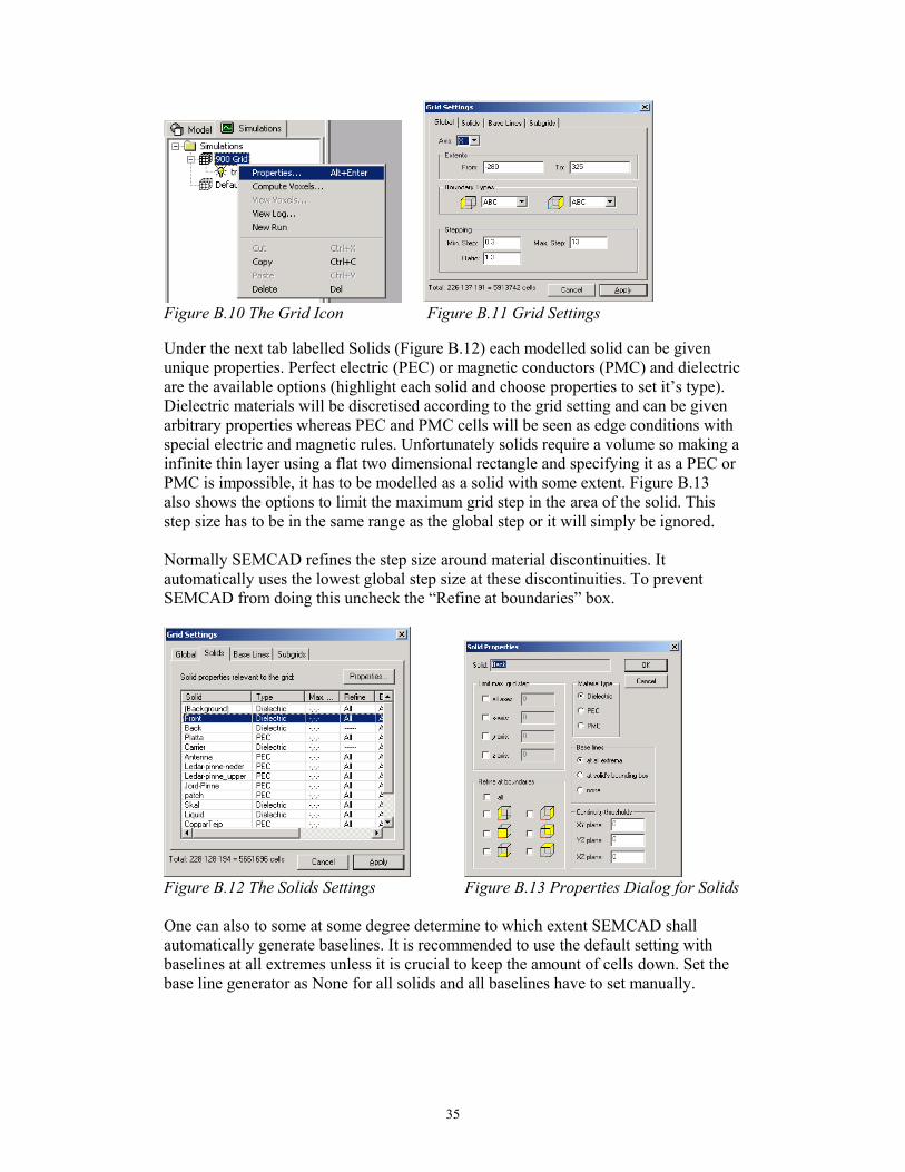
35
Figure B.10 The Grid Icon Figure B.11 Grid Settings Under the next tab labelled Solids (Figure B.12) each modelled solid can be given unique properties. Perfect electric (PEC) or magnetic conductors (PMC) and dielectric are the available options (highlight each solid and choose properties to set it’s type). Dielectric materials will be discretised according to the grid setting and can be given arbitrary properties whereas PEC and PMC cells will be seen as edge conditions with special electric and magnetic rules. Unfortunately solids require a volume so making a infinite thin layer using a flat two dimensional rectangle and specifying it as a PEC or PMC is impossible, it has to be modelled as a solid with some extent. Figure B.13 also shows the options to limit the maximum grid step in the area of the solid. This step size has to be in the same range as the global step or it will simply be ignored. Normally SEMCAD refines the step size around material discontinuities. It automatically uses the lowest global step size at these discontinuities. To prevent SEMCAD from doing this uncheck the “Refine at boundaries” box.
Figure B.12 The Solids Settings Figure B.13 Properties Dialog for Solids One can also to some at some degree determine to which extent SEMCAD shall automatically generate baselines. It is recommended to use the default setting with baselines at all extremes unless it is crucial to keep the amount of cells down. Set the base line generator as None for all solids and all baselines have to set manually.

36
Continuity thresholds are useful for solids with complex shapes or solids that are not aligned with any grid axes. The continuity thresholds set the distance in grid lines that each cell can have and still get reconnected. This should only be used if a complex shape like a helix antenna looks fragmented or has missing edges. The next tab shows the base lines that have been automatically generated with respect to the dielectric solids that make up our model (Figure B.14). Here one can set the minimal and maximum step size that can be used between the intervals (on the right side of the given base line). Step sizes that are outside the global step sizes (as shown in Figure B.15) will be ignored. It is important to visualise that the model you have made will be discretised into single cells, atoms or voxels as SEMCAD labels them from the perfect shapes of your model. And it is these base lines that govern the size of each voxel. The result will not contain any perfect shapes like spheres and cylinders as we have modelled but approximations. Some complex shapes may have generated an uncalled amount of baselines and some shapes may have too few baselines to get a faithful representation when approximated with the rectangular voxels, so it is highly recommended that one check the model before starting simulations. The user can add and remove base lines without any limitations. When modelling thin layers or any small sized object it is wise to model them a few cells thick. If that depth is in the same magnitude as the minimal step size a few baselines should be added on the correct axis instead of lowering the global minimal grid-step, which could seriously increase the computation time. The Subgrids tab should be ignored until it has been implemented. It is unknown when this feature will be available.
Figure B.14 Base Lines Figure B.15 Compute and View Voxels

37
B.5 Model Visualisation Now that the grid settings have been set, choose Compute Voxels (highlight and right click the grid icon as shown in Figure B.15). It discretises our model and updates each cells (voxel) properties. This can be seen as a transformation from our geometrically perfect CAD model into a three-dimensional database with each cell’s properties. These voxels can be visualised and it is recommended that one check the results before simulating. To do this choose View Voxels (as Figure B.15 shows) and make sure that each part of the model has a faithful representation and that every solid really is connected. A certain amount of stair casing is for some of the more complex objects more or less impossible to get rid of, or as the case most often would be a waste of simulation time. Figure B.16 shows how a sphere can end up looking. In our case we have decreased the step sized on the part that interferes with the telephone. A more faithful representation of the backside of the bowl as well is probably not worth the extra time spent calculating. The easiest way to check the geometry is to show the voxels only and not together with the original solids (uncheck Original Solids like Figure B.17 shows). Only the voxels that are included in the slice are now shown. Using a mouse with a scroll wheel makes it very easy to check each slice. Just highlight the box containing the coordinate that isn’t frozen and scroll up and down all along the model using the scroll wheel. Everything should be ready for simulation if the approximated models look acceptable and each solid has a minimum depth of a few cells.
Figure B.16 A Stair Cased Bowl Figure B.17 Voxel Viewer B.6 Simulation Settings Next up are the simulation settings. Highlight the light bulb icon and using the right mouse button and choose properties (as Figure B.18). This brings up the run settings and the global tab (Figure B.19), where one chooses if the simulation shall run in harmonic (single frequency) or transient mode (a span of frequencies with a gaussian pulse). In harmonic mode it is recommended to set the simulation time in periods (only possible in harmonic mode) and for transient in seconds. Ten periods is usually long enough for simulations in harmonic mode to reach the steady state. For transient mode the simulation time depends on the input source and should be decided based on the layout of the input signal, more about this later.

38
Figure B.18 Run Settings Figure B.19 Global Settings Every simulation is a trade-off between simulation time and end result, which brings us to the next settings: the absorbing boundary dialog. The PML algorithm is better and preferred for simulations with less free space surrounding the model. We tested both Mur and PML with 25 to 30 cm of free space around the phone in all six directions. The PML computation took twice as long time as the one using second order Mur though both S11 graphs came out identical. Having plenty of free space around the simulated object probably affects the result in a positive way more than choosing the most accurate boundary condition available. It is safe to say that one should leave the settings unaltered for PML and Higdon conditions unless you really know what you are doing. MUR can be set as first or second order only. Figure B.20 shows the Absorbing Boundaries settings.
Figure B.20 Absorbing Boundaries Settings Figure B.21 Edge Source Dialog Figure B.21 shows the properties for the Edge Source expanded. As mentioned earlier it is recommended to run the Edge Source as a Voltage Source for these types of simulations. The source resistance must be set for a voltage source since the Voltage Source has an internal resistor taking energy out of the grid. With a Hard Source these waves would have been reflected instead of taken out of the grid at the source. The Added Source just adds a field-strength on top of the value already calculated with the Yee algorithm. The advantage with the Voltage Source is that the excitation signal decays faster thus reaching steady state earlier and saves simulation time. If a Gaussian Sine is chosen its characteristics can be set by pressing Properties as shown at the bottom of the screenshot on labelled Figure B.21. This will bring up Figure B.23 to your attention.

39
Figure B.22 TPeak and TSigma Figure B.23 Signal Settings The simulation duration should be at least two times TSigma, to make sure that the simulation will reach the steady state. A suitable value for TPeak would be three times TSigma to ensure that the start of the pulse doesn’t get too steep. Figure B.22 shows how TPeak and TSigma describe the signal. These values also determine the frequency contents of the gaussian sine. If there is a wide range of frequencies included like one would require for simulating both GSM and DCS bands at the same time, the power of these frequencies may be too small since one has to set a centre frequency. This can be seen in Figure B.23 the graph in the bottom plot. Here we have a preview of a gaussian sine with a fairly broad frequency content, with less power around the centre frequency. If TSigma were doubled we would have seen a narrower spectrum and more power around 900MHz. Using a centre frequency of say 1400MHz to simulate both 900 MHz and 1800 MHz yields not enough power for the interesting frequencies according to our tests. Strange things usually happen on S11 plots for frequencies with next to none power. Using two sources each transmitting on one band didn’t get acceptable results either. Therefore we must recommend that each band should be simulated one at a time.
Figure B.24 Lumped Elements Settings If the model has any lumped elements they will be listed under the sensors and lumped elements tab. Highlight the lumped element of your choice and press properties and the a box should pop up presenting the available settings (Figure B.24). Depending on the circuit type that is checked the two input boxes adapts and shows the correct units.
40
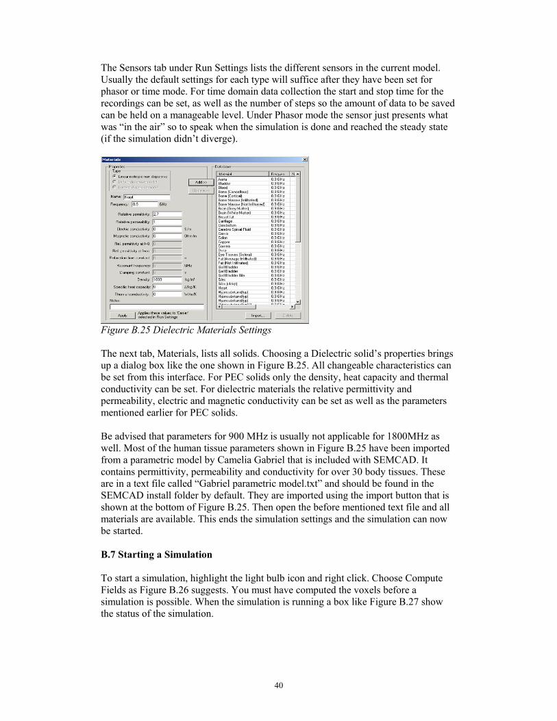
The Sensors tab under Run Settings lists the different sensors in the current model. Usually the default settings for each type will suffice after they have been set for phasor or time mode. For time domain data collection the start and stop time for the recordings can be set, as well as the number of steps so the amount of data to be saved can be held on a manageable level. Under Phasor mode the sensor just presents what was “in the air” so to speak when the simulation is done and reached the steady state (if the simulation didn’t diverge).
Figure B.25 Dielectric Materials Settings The next tab, Materials, lists all solids. Choosing a Dielectric solid’s properties brings up a dialog box like the one shown in Figure B.25. All changeable characteristics can be set from this interface. For PEC solids only the density, heat capacity and thermal conductivity can be set. For dielectric materials the relative permittivity and permeability, electric and magnetic conductivity can be set as well as the parameters mentioned earlier for PEC solids. Be advised that parameters for 900 MHz is usually not applicable for 1800MHz as well. Most of the human tissue parameters shown in Figure B.25 have been imported from a parametric model by Camelia Gabriel that is included with SEMCAD. It contains permittivity, permeability and conductivity for over 30 body tissues. These are in a text file called “Gabriel parametric model.txt” and should be found in the SEMCAD install folder by default. They are imported using the import button that is shown at the bottom of Figure B.25. Then open the before mentioned text file and all materials are available. This ends the simulation settings and the simulation can now be started. B.7 Starting a Simulation To start a simulation, highlight the light bulb icon and right click. Choose Compute Fields as Figure B.26 suggests. You must have computed the voxels before a simulation is possible. When the simulation is running a box like Figure B.27 show the status of the simulation.

41
If your computer accesses the hard drive a lot during the simulation, take that as a warning. Say for example a processor running at 500 MHz. A single clock cycle then has a duration of 2 nanoseconds. A standard IDE hard drive running at 7200 rpm has an average seek time somewhere around 10 milliseconds, whereas the seek time of standard SDRAM usually is advertised as somewhere around 10 nanoseconds or faster. Quite a few more clock cycles are lost waiting for the hard drive compared to fetching data from RAM, so the computation time can be increased by a large factor with heavy hard drive access. Either get more RAM or decrease the number of cells used in the simulation.
Figure B.26 Starting a Simulation Figure B.27 Almost Done! B.8 Post-Processing When the simulation is done the cancel box shown at the bottom right of Figure B.27 will be labelled with close instead. Click close and you will find something like Figure B.28, where every sensor is presented and their respective post processing options. Please note that if you edit the model or grid settings in any way all simulation results will be erased for that particular project.
Figure B.28 Choosing Post Processor

42
The field sensor used in this simulation presents a variety of outputs as Figure B.28 shows (labelled Unnamed at the top in our case). For SAR presentations the recommended way to present the statistics is to overlay them in the model (Figure B.29). This is mainly because it is easier to check SAR at different positions and the statistics box will give you the global maximum values if you feel that that is enough. The Contour view shows a 2D graphical plot but is painfully slow if you have not beforehand settled on which slice to display. A surface plot is in 3D and can be somewhat difficult to navigate in.
Figure B.29 Modes of Presentation Field quantities are displayed on top of the 3D model in a rectangular plane of your choice. There are two different SAR measures available for display. Peak SAR simply presents the peak SAR without any averaging for mass and the IEEE-1529 uses an algorithm for averaging over mass (for example 1 or 10 grams) according to the draft with the same name. Both can use source power as input for normalisation. The peak SAR post processor is useful for determining where local SAR peaks are located and presents an easy way to see how SAR decreases as one gets further and further away from the radiating source. Highlight Peak SAR from under the Edge Source, press the right mouse button and choose Overlay in model. The next dialog box lists the solids in your model and an input box for normalising the input power. To the left of each listed solid is a box, indication if crossed that that solid will be used for SAR computation. Press the OK button when done and after some processing a sliced view similar to the one available when checking voxels in Figure B.17 appears. Figure B.31 shows the information box that accompanies the standard 3D model view. In order to see the graphical overlay inside the solid you chose earlier switch to wire frame or facets mode instead of shaded. The real information is just a mouse click away though; press the statistics button shown at the top right of Figure B.31. Something resembling Figure B.30 should appear at the left side of the screen. This presents the top SAR value at the current slice as well as the global maximum complete with coordinates. To check the SAR value at different parts of the bowl choose an axis to slice and scroll your way around the bowl while looking at the statistics box and the value to the right of where it says “Slice Maximum field value (current settings)”.

43
Figure B.30 Statistical Peak SAR Information Figure B.31 Sliced SAR For IEEE-1529 averaged SAR there are a few things to think about. One must set the type of each solid that is to be used for SAR computation. Each body mass must be set as “body tissue” or “extremities tissue” due to the difference in the compliance tests for extremities as hands, wrist, ankles and the external ear. When simulating handsfree sets or phones that is not positioned in a talk position specify extremities. When averaging, only the SAR from the type of tissue that the chosen mass belongs to is used for calculation. The same display possibilities that the peak SAR offers are available for averaged SAR as well, but with all values averaged.

44
Appendix C MapSAR manual C.1 Introduction This manual will concentrate on the basics regarding the software included with the MapSAR bench top SAR assessment system. Only the basic functions regarding SAR measurements are included here, for more information about calibration issues consult the MapSAR documentation bundled with the product [10].
Figure C.1 MapSAR Graphical User Interface C.2 Description of the Graphical User Interface After starting the MapSAR software the program’s interface appears on the top of the desktop. A screenshot is shown in Figure C.1. For SAR measurements the centre of attention will be at the upper left windows that displays the continuous and peak SAR-readings. Figure C.2 shows the two displays with the continuous readings at the top and the max SAR value below. The max SAR value is the highest encountered SAR reading during the measurement.
Figure C.2 Continuous (top box) and Maximal (bottom box) SAR Readings
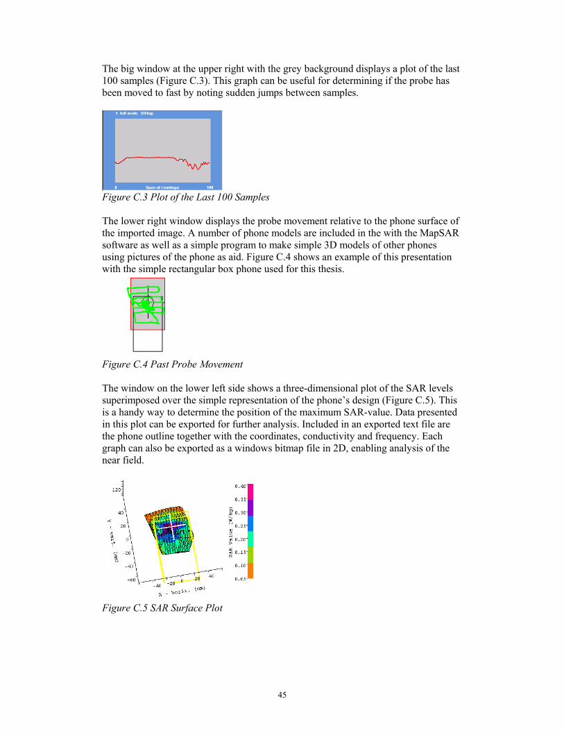
45
The big window at the upper right with the grey background displays a plot of the last 100 samples (Figure C.3). This graph can be useful for determining if the probe has been moved to fast by noting sudden jumps between samples.
Figure C.3 Plot of the Last 100 Samples The lower right window displays the probe movement relative to the phone surface of the imported image. A number of phone models are included in the with the MapSAR software as well as a simple program to make simple 3D models of other phones using pictures of the phone as aid. Figure C.4 shows an example of this presentation with the simple rectangular box phone used for this thesis.
Figure C.4 Past Probe Movement The window on the lower left side shows a three-dimensional plot of the SAR levels superimposed over the simple representation of the phone’s design (Figure C.5). This is a handy way to determine the position of the maximum SAR-value. Data presented in this plot can be exported for further analysis. Included in an exported text file are the phone outline together with the coordinates, conductivity and frequency. Each graph can also be exported as a windows bitmap file in 2D, enabling analysis of the near field.
Figure C.5 SAR Surface Plot

46
The ‘Button status’ window indicates whether the Wacom board is active (Figure C.6), i.e. if the drawing board senses where the pen is. Before measurement runs are started the software will display a prompt to make sure that the pen is ready.
Figure C.6 Button Status To the lower right of the 3D plot is a window (Figure C.7) displaying the number of samples collected during each measurement so far. The maximum number of points or coordinates that can be collected are 200. This means that the plot will always have a limit of 200 coordinates but it is possible to search for the max SAR value for as long as wanted.
Figure C.7 Collected Points The Collect button (Figure C.8) starts and stops every measurement session. Each measurement can also be initiated, started/ and stopped using the sequence C, S and F. After pressing C the software will check if the pen is ready and prompt the user to do the necessary actions. Pressing S after that will start the measurements. To finish the measurements and redraw the 3D-plot press F.
Figure C.8 The Collect Button When the measurements are done press ‘P’ or the Process button to compute the 1-gram and 10-gram averaged SAR. Note that the decimal separator used must not be a comma as is the standard for the Swedish keyboard layout in windows. Choose points as the decimal separator in the Control panel/Regional Settings/Numbers. MapSAR will crash when it attempts to compute the average using commas.
Figure C.9 Averaged SAR Levels

47
Figure C.9 shows an example of the averaged SAR presentation. The cheek factor correction factor is for comparison with MapSAR and other measurements methods. Due to the relatively high thickness of the sphere used to contain the liquid for MapSAR for comparisons with results acquired with other measurement systems with cheek that is not as thick. 2mm is a common shell thickness for a SAM phantom whereas the MapSAR pyrex bowl is 4mm thick. And it is to compensate for this difference that the SAR averages may need to be multiplied with this factor. At least theoretically this extra thick shell should result in a lower value for MapSAR measurements.
Figure C.10 Cheek Correction Calibration The cheek factor needs to be calibrated and the settings for this is under MathOptions|Wall Correction. Figure C.10 shows the dialog box for estimating SAR with thinner shell. When calibrating the phone is turned on and positioned with a 0,2,4,6 and 8 mm to the bowl and each of these values is taken by pressing the Get SAR buttons. The extrapolation of the measured values can be done in two ways as Figure C.10 shows, with a 4th order polynomial or with a linear logarithmic fit. C.3 Step by Step Measurements Guide for MapSAR i.) Position the phone in the positioning rack. ii.) Start the phone and the amplifier/data converter. iii.) Activate the Wacom board by lifting the pen and releasing it on the board and
check the button status window for *ON*. iv.) Press C to initiate the measurements. v.) Press S to start the measurements. vi.) Start moving the pointing device along the predefined mask on the board and
check for hotspots (i.e. SAR peaks). vii.) Return to the hotspots for a thorough sweep. viii.) Press F to stop the measurements when done. ix.) Save the desired data, note the max SAR value, press P to compute average.

48
Appendix D: Measurements Results D.1 Measurement Results Mat. Ground
Pos. Display Display
Patch Resistors Gap 2mm E[SAR] Std. Dev.
(%) Max. Dev. (%)
None None None None None No 0.4209 1.43 2.89 Cu Floating None None None No 0.4612 2.00 3.86 Cu A None None None No 0.4626 1.84 3.33 Cu B1 None None None No 0.4299 1.69 2.82 Cu B2 None None None No 0.4694 2.11 3.75 Cu B1+ B2 None None None No 0.4280 3.15 6.09 Cu C None None None No 0.5275 1.43 2.93 Cu D None None None No 0.3656 4.57 9.18 Cu E1 None None None No 0.4214 1.77 3.24 Cu E2 None None None No 0.4481 2.21 4.04 Cu E1+ E2 None None None No 0.3274 3.38 6.84 Cu F1 None None None No 0.4548 1.57 3.24 Cu F2 None None None No 0.4597 1.45 3.85 Cu F1+ F2 None None None No 0.4239 2.24 3.98 Al Floating None None None No 0.4203 3.39 5.65 Al A None None None No 0.4352 1.64 3.71 Al B1 None None None No 0.4246 3.16 5.75 Al B2 None None None No 0.4345 2.86 4.73 Al B1+ B2 None None None No 0.4129 2.44 6.09 Al C None None None No 0.4512 2.82 5.95 Al D None None None No 0.3646 3.55 8.08 Al E1 None None None No 0.3901 1.56 2.58 Al E2 None None None No 0.4194 2.85 4.61 Al E1+ E2 None None None No 0.3164 2.16 5.50 Al F1 None None None No 0.4108 1.71 3.35 Al F2 None None None No 0.4236 2.34 5.06 Al F1+ F2 None None None No 0.4000 1.86 3.76 Cu Floating Yes Yes None No 0.3993 4.16 9.83 Cu Floating Yes None None No 0.4047 2.87 8.23 Cu B1+ B2 Yes None None No 0.3565 3.84 6.61 Cu F1+ F2 Yes None None No 0.4046 5.12 10.49 Cu D Yes None None No 0.8482 4.83 7.76 Cu E1+ E2 Yes None None No 2.0000 Cu Floating Yes None 10 middle. Yes 0.4186 1.87 4.67 Cu Floating Yes None 20 parallel. Yes 0.3291 0.34 7.28 Cu Floating Yes None 5 middle. Yes 0.3873 1.39 2.76 Cu Floating Yes None 10 parallel. Yes 0.3382 2.35 4.76 Cu Floating Yes Yes 20 parallel. Yes 0.3381 2.21 3.86 Cu Floating Yes Yes None Yes 0.3964 2.40 5.39 Cu Floating Yes None None Yes 0.3779 3.47 6.05 Table D.1 Measurement Results

49
D.2 Reference Designs: Near Field-Plots
Figure D.1 Reference Designs As Figure D.2-5 shows the near-field pattern is more or less the same for all the designs in Figure D.1.
Figure D.2 No Front Layer Figure D.3 Floating Front Layer
Figure D.4 2-mm Gap, Display Opening Figure D.5 2-mm Gap, Display Patch

50
D.3 Ground Positions: Near Field-Plots
Figure D.6 Ground Position Designs As seen in Figures D.7-18 the SAR-distribution is altered, moved towards the ground positions.
Figure D.7 a-position Figure D.8 b1-position
Figure D.9 b2-position Figure D.10 b1+b2-positions

51
Figure D.11 c-position Figure D.12 d-position
Figure D.13 e1-position Figure D.14 e2-position
Figure D.15 e1+e2-positions Figure D.16 f1-position
Figure D.17 f2-position Figure D18 f1+f2-position

52
D.4 Resistors: Near Field-Plots
Figure D.19 Resistor Designs
Figure D.20 R = 10Ω at the centre Figure D.21 R = 5Ω at the centre
Figure D.22 R = 20Ω parallel Figure D.23 R = 10Ω parallel
Figure D.24 R = 20Ω parallel

53
D.5 Ground Positions with Display: Near Field Plots
Figure D.25 Ground Positions with Display
Figure D.26 b1+b2 positions, with display Figure D.27 e1+e2 positions, with display patch
Figure D.28 e1+e2 positions, with display

54
Appendix E: Numerical Results of SEMCAD Simulations. E.1 Perfect Conducting Front Layer Ground Position Peak SAR closest to phone [W/Kg] Maximum Peak SAR in sphere [W/Kg]
None (floating) 0,186357 0,196045 A 0,184994 0,191504 B1 0,185902 0,194241 B2 0,187301 0,19579 B1 + B2 0,162361 0,234088 C 0,157585 0,218583 D 0,166481 0,173116 E1 0,181765 0,189511 E2 0,187301 0,19579 E1 + E2 0,186065 0,222201 F1 0,181778 0,189518 F2 0,18625 0,194907 F1 + F2 0,154675 0,174432 E.2 Perfect Conducting and Non Perfect Layers Comparison Front Layer Model (Same thickness used for all cases)
Peak SAR closest to phone [W/Kg]
Maximum Peak SAR in sphere [W/Kg]
Perfect Conducting 0,184994 0,191504 Copper Characteristics 0,185109 0,191589 Aluminium Characteristics 0,185108 0,191588 E.3 Resistor Simulations without Display Opening Resistor Configuration Peak SAR closest to phone [W/Kg] Maximum Peak SAR in sphere [W/Kg]
10 Ω center 0,162431 0,174838 5 Ω center 0,152723 0,167916 10 Ω at each side 0,163535 0,186103 20 Ω at each side 0,167821 0,184803 E.4 Resistor Simulations with Display Opening Resistor Configuration Peak SAR closest to phone [W/Kg] Maximum Peak SAR in sphere [W/Kg]
No resistors 0,189633 0,19619 5 Ω center 0,186689 0,186689 10 Ω center 0,162 0,178083 5 Ω at each side 0,174327 0,184308 20 Ω at each side 0,162075 0,17622 20 Ω at each side (With display patch)
0,161911 0,181582
E.5 No Front Layer Ground Position Peak SAR closest to phone [W/Kg] Maximum Peak SAR in sphere [W/Kg]
None (floating) 0,171927 0,195298

55
Appendix F: DASY3 Measurements F.1 DASY3 Results These were made in order to get some reliable averaged SAR values for comparisons. Also the question remained if using an Aluminium or Copper front really made a difference or if they both gave the phone the same electromagnetic properties. A single measurement with ground positions were made with the phone in a tilted position with the lower part of the phone, that MapSAR and SEMCAD shows to be the hotspot, very close to the cheek of the phantom. The DASY3 probe managed thus to get much closer to the hotspot than possible with the MapSAR equipment (at least for the way we positioned the phone), thus resulting in a completely different reading for the case with grounds at E1+E2. Figures F.1-F.4 shows the SAR distributions over the phone surface. Test Case 1 gram Average Peak SAR 10 gram average
No metal layer 0.651 0.928 0.442 Copper layer 0.483 0.721 0.313 Aluminium layer 0.541 0.773 0.368 Ground at E1+E2 0.368 0.718 0.228 Table F.1 DASY3 Left Cheek Measurements. F.2 DASY3 SAR Distribution Plots
Figure F.1 SAR Distribution with No Metal Layer

56
Figure F.2 SAR Distribution with Copper Front Layer
Figure F.3 SAR Distribution with Aluminium Front Layer

57
Figure F.4 SAR Distribution with Grounds at E1+E2
58
Appendix G: Acronyms ABC Absorbing Boundary Condition ANSI American National Standard Institute CAD Computer-Aided Design CBC Conducting Boundary Condition CENELEC European Committee for Electrotechnical Standardization DASY Dosimetric Assessment System DCS Digital Communications System EMC Electromagnetic Compatibility EMI Electro Magnetic Interference FDTD Finite Difference Time Domain FEM Finite Element Method GSM Global System for Mobile Communications GUI Graphical User Interface ICNIRP International Commission for Non-Ionizing Radiation Protection IDE Integrated Drive Electronics IE3D Integral Equations in 3 Dimensions IEEE Institute of Electrical and Electronics Engineers MoM Method of Moment ORBC Outer Boundary Condition PBC Periodic Boundary Condition PC Personal Computer PCB Printed Circuit Board PEC Perfect Electrically Conductor PIFA Planar Inverted F Antenna PMC Perfect Magnetically Conductor PML Perfectly Matched Layer RAM Random Access Memory RL Return Loss RF Radio Frequency rms root mean square SAM Specific Anthropomorphic Mannequin SAR Specific Absorption Rate SDRAM Synchronous Dynamic Random Access Memory SEMCAD Simulator for Electromagnetic Compatibility, Antennas and Dosimetry SPEAG Schmid & Partner Engineering AG SWR Standing Wave Ratio VSWR Voltage Standing Wave Ratio