a continuous-time sigma-delta a-d converter in an inp ... · a continuous-time sigma-delta a-d...
TRANSCRIPT
UNIVERSITY of CALIFORNIASanta Barbara
A Continuous-Time Sigma-Delta A-D Converter
in an InP-based HBT Technology
A Dissertation submitted in partial satisfaction of the
requirements for the degree
Doctor of Philosophy
in
Electrical and Computer Engineering
by
Sundararajan Krishnan
Committee in charge:
Professor Mark J. W. Rodwell, ChairProfessor Steve ButnerProfessor Steve LongProfessor Umesh MishraJoseph Jensen, Hughes Research Labs, Malibu
September 2002

The dissertation of Sundararajan Krishnan is approved.
Professor Steve Butner
Professor Steve Long
Professor Umesh Mishra
Joseph Jensen, Hughes Research Labs, Malibu
Professor Mark J. W. Rodwell, Committee Chair
June 2002

A Continuous-Time Sigma-Delta A-D Converter in an InP-based HBT
Technology
Copyright c° 2002
by
Sundararajan Krishnan
iii

iv

Acknowledgements
Working for Prof. Rodwell has been a pleasure and a privilege. His ability to
answer the most intriguing of questions, with the utmost ease, and often on the
spur of the moment, will never cease to amaze me. None of the results in this
work would have been possible, if not for him. To him, I owe much more than I
can ever express in words.
The other members of the committee, Prof. Steve Butner, Prof. Steve Long,
Prof. Umesh Mishra, and Joe Jensen have been very supportive. I thank them
for their comments and suggestions. I would like to thank Joe in particular for
his help in testing the ADC.
Most of my graduate student life was spent in the clean room and life would
have been a lot more miserable if not for Jack, Brian, Bob, Mike and Neil. Thanks
for working so hard to keep everything operational in the clean room.
Thanks are also due to other members of the Rodwell Empire. to Dino, James,
Michelle, Shri, Karthik, Yoram and Thomas for teaching me the ropes; to Yun
for helping me with the process; to Dennis for his views on humans and human
nature; to Miguel for discussions ranging from Super Star to Globalization; to
Zach for being a Sacramento Kings’ fan; to Mattias for being Swedish; to Paidi
for liberal use of his car and to Navin for his wonderful dinners.
The testing of the ADC would not have been possible without the assistance
of a number of people. Thanks to Tommy Luna and Joe Jensen of HRL for the
DEMUX, to Shri for the limiting amp, to Jerry, Bob, and the Mishra and York
group for the innumerable parts that we borrowed.
And finally, to my parents, without whose sacrifices, I would never have come
this far.
v
Curriculum VitæSundararajan Krishnan
1994—1998 B.Tech. in Electrical EngineeringIndian Institute of Technology, Madras
1998—1999 M. S. in Electrical and Computer EngineeringUniversity of California, Santa Barbara
1999—2002 Ph. D. in Electrical and Computer EngineeringUniversity of California, Santa Barbara
Fields of StudyHigh-speed devices and circuits
Publications
S. Krishnan, D. Scott, Z. Griffith, M. Urteaga, Y. Wei,M. Dahlstrom, N. Parthasarathy and M. J. W. Rodwell, “An8-GHz continuous-time Σ − ∆ modulator in an InP-basedMesa DHBT Technology,” submitted to ISSCC, 2003
S. Krishnan, Z. Griffith, M. Urteaga, Y. Wei, D. Scott,M. Dahlstrom, N. Parthasarathy and M. J. W. Rodwell, “87GHz Frequency Dividers in an InP-based Mesa DHBT Tech-nology,” to be presented at IEEE GaAs IC Symposium, 2002
S. Krishnan, M. Dahlstrom, T. Mathew, Y. Wei, D. Scott,M. Urteaga, M. J. W. Rodwell, W. K. Liu, D. Lubyshev,X. M. Fang and Y. Wu , “InP/InGaAs/InP Double Heteron-junction Bipolar Transistors with 300 GHz fmax,”IndiumPhosphide and Related Materials, Nara, Japan, 2001
S. Krishnan, S. Jaganathan, T. Mathew, Y. Wei andM. J. W. Rodwell, “Broadband HBT amplifiers,” 2000 IEEECornell Conference on High Speed Electronics
S. Krishnan, D. Mensa, J. Guthrie, S. Jaganathan, Y. Wei,T. Mathew, R. Girish and M. J. W. Rodwell, “Broadband
vi

lumped HBT amplifiers,” IEE Electronics Letters, March2000
S. Jaganathan, S. Krishnan, D. Mensa, T. Mathew, Y. Betser,Y. Wei, D. Scott, M. Urteaga and M. J. W. Rodwell, “An 18GHz Continuous-Time Σ−∆ Analog-Digital Converter Im-plemented in InP-Transferred Substrate HBT Technology,”IEEE Journal of Solid State Circuits, September 2001
vii

Abstract
A Continuous-Time Sigma-Delta A-D Converter in an InP-based HBT
Technology
by
Sundararajan Krishnan
A 2nd order continuous-time Σ−∆ modulator, clocked at 8 GHz, is demon-
strated. A static frequency divider, operating to a maximum clock frequency of 87
GHz, is also demonstrated. These designs are motivated by the explosive growth
in the fiber-optic and telecommunication market.
The first part of the thesis focuses on the development of InP-based Double
Heterojunction Bipolar Transistors (DHBTs) in a substrate-transfer process as
well as in a narrow-mesa process. The design of a Static Frequency Divider in
the narrow-mesa process is also discussed. The main results of this part of the
thesis are: (i) a device with 165 GHz fτ , 300 GHz fmax and 9 V BVCEO in a
substrate-transfer process, (ii) a device with 200 GHz fτ , 205 GHz fmax and 6
V BVCEO in a narrow-mesa process, and (iii) a static frequency divider with a
maximum clock frequency of 87 GHz.
The focus shifts in the second part of the thesis to the design of a 2nd order
continuous-time Σ−∆ modulator in the narrow-mesa process. The problem of
metastability and excess loop delay is considered. Solutions to these problems,
based on theoretical analysis, are proposed and their efficacy is studied using
full-loop MATLAB and SPICE simulations. Finally, the measurement techniques
and the results are discussed. The measured SNR, and effective bits of reso-
lution, at 250 Msps sample-rate are 48 dB and 7.7 bits, respectively. A peak
intermodulation-suppression of > 80 dBc is observed.
viii
Contents
List of Tables xi
List of Figures xii
1 Introduction 11.1 Transistor technologies for mixed-signal applications . . . . . . . . 21.2 HBTs by substrate transfer . . . . . . . . . . . . . . . . . . . . . 31.3 Narrow-mesa HBTs . . . . . . . . . . . . . . . . . . . . . . . . . . 51.4 Σ−∆ ADC Design . . . . . . . . . . . . . . . . . . . . . . . . . . 6
2 DHBTs by substrate-transfer 82.1 SHBT (vs) DHBT . . . . . . . . . . . . . . . . . . . . . . . . . . 8
2.1.1 Variations in Epitaxial Layer Structure . . . . . . . . . . . 92.1.2 Process Development . . . . . . . . . . . . . . . . . . . . . 10
2.2 Results . . . . . . . . . . . . . . . . . . . . . . . . . . . . . . . . . 142.2.1 DC Performance . . . . . . . . . . . . . . . . . . . . . . . 142.2.2 Microwave performance . . . . . . . . . . . . . . . . . . . . 15
3 Narrow-mesa HBTs 203.1 Realizing Medium Scale Integration ICs . . . . . . . . . . . . . . . 203.2 Mesa-HBT Technology: Process Features . . . . . . . . . . . . . . 233.3 Mesa-HBT Results . . . . . . . . . . . . . . . . . . . . . . . . . . 283.4 Static Frequency Divider . . . . . . . . . . . . . . . . . . . . . . . 30
4 Σ−∆ ADC Theory 354.1 Linearized Theory . . . . . . . . . . . . . . . . . . . . . . . . . . . 364.2 Performance modeling of a 2nd order Σ−∆ modulator . . . . . . 394.3 Ideal Loop-Performance . . . . . . . . . . . . . . . . . . . . . . . 40
ix
5 Design Methodology 435.1 Metastability . . . . . . . . . . . . . . . . . . . . . . . . . . . . . 455.2 Excess Delay . . . . . . . . . . . . . . . . . . . . . . . . . . . . . 525.3 Circuit Design . . . . . . . . . . . . . . . . . . . . . . . . . . . . . 62
5.3.1 Integrator-1 . . . . . . . . . . . . . . . . . . . . . . . . . . 625.3.2 Integrator-2 . . . . . . . . . . . . . . . . . . . . . . . . . . 665.3.3 Comparator . . . . . . . . . . . . . . . . . . . . . . . . . . 685.3.4 NRZ and RTZ DAC . . . . . . . . . . . . . . . . . . . . . 68
6 ADC Results 736.1 Σ−∆ ADC: Test Set-Up . . . . . . . . . . . . . . . . . . . . . . 736.2 Measured Results : Analog method . . . . . . . . . . . . . . . . . 756.3 Measured Results : Digital Acquisition method . . . . . . . . . . 76
6.3.1 One-tone Measurements . . . . . . . . . . . . . . . . . . . 776.3.2 Two-tone Measurements . . . . . . . . . . . . . . . . . . . 80
7 Conclusions and Future Work 847.1 Summary of achievements . . . . . . . . . . . . . . . . . . . . . . 847.2 Future Work . . . . . . . . . . . . . . . . . . . . . . . . . . . . . . 86
Bibliography 88
A Process Flow 95
x
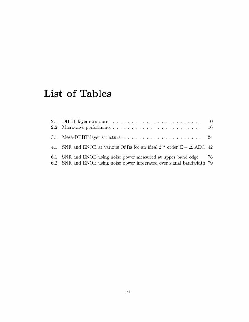
List of Tables
2.1 DHBT layer structure . . . . . . . . . . . . . . . . . . . . . . . . 102.2 Microwave performance . . . . . . . . . . . . . . . . . . . . . . . . 16
3.1 Mesa-DHBT layer structure . . . . . . . . . . . . . . . . . . . . . 24
4.1 SNR and ENOB at various OSRs for an ideal 2nd order Σ−∆ ADC 42
6.1 SNR and ENOB using noise power measured at upper band edge 786.2 SNR and ENOB using noise power integrated over signal bandwidth 79
xi
List of Figures
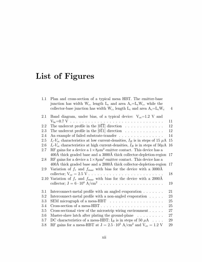
1.1 Plan and cross-section of a typical mesa HBT. The emitter-basejunction has width We, length Le and area Ae=LeWe, while thecollector-base junction has width Wc, length Lc and area Ac=LcWc 4
2.1 Band diagram, under bias, of a typical device: Vce=1.2 V andVbe=0.7 V . . . . . . . . . . . . . . . . . . . . . . . . . . . . . . . 11
2.2 The undercut profile in the [011] direction . . . . . . . . . . . . . 122.3 The undercut profile in the [011] direction . . . . . . . . . . . . . 122.4 An example of failed substrate-transfer . . . . . . . . . . . . . . . 142.5 Ic-Vce characteristics at low current-densities, IB is in steps of 15 µA 152.6 Ic-Vce characteristics at high current-densities, IB is in steps of 50µA 162.7 RF gains for a device a 1×8µm2 emitter contact. This device has a
400A thick graded base and a 3000A thick collector-depletion-region 172.8 RF gains for a device a 1×8µm2 emitter contact. This device has a
400A thick graded base and a 2000A thick collector-depletion-region 172.9 Variation of fτ and fmax with bias for the device with a 3000A
collector; Vce = 2.5 V . . . . . . . . . . . . . . . . . . . . . . . . . 182.10 Variation of fτ and fmax with bias for the device with a 2000A
collector; J = 6 · 104 A/cm2 . . . . . . . . . . . . . . . . . . . . . 19
3.1 Interconnect-metal profile with an angled evaporation . . . . . . . 213.2 Interconnect-metal profile with a non-angled evaporation . . . . . 233.3 SEM micrograph of a mesa-HBT . . . . . . . . . . . . . . . . . . 253.4 Cross-section of a mesa-HBT . . . . . . . . . . . . . . . . . . . . . 253.5 Cross-sectional view of the microstrip wiring environment . . . . . 273.6 Master-slave latch after plating the ground-plane . . . . . . . . . 273.7 DC characteristics of a mesa-HBT; IB is in steps of 50 µA . . . . 293.8 RF gains for a mesa-HBT at J = 2.5 · 105 A/cm2 and Vce = 1.2 V 29
xii

3.9 Divider : Circuit Schematic . . . . . . . . . . . . . . . . . . . . . 313.10 Divider Measurement Setup : 4-40 GHz . . . . . . . . . . . . . . . 313.11 Output Voltage at 2 GHz; fclk = 4 GHz . . . . . . . . . . . . . . . 323.12 Divider Measurement Setup : 50-75 GHz . . . . . . . . . . . . . . 333.13 Output Voltage at 37.5 GHz; fclk = 75 GHz . . . . . . . . . . . . 333.14 Divider Measurement Setup : 75-110 GHz . . . . . . . . . . . . . 343.15 Output Voltage at 43.5 GHz; fclk = 87 GHz . . . . . . . . . . . . 34
4.1 Block Diagram of a Σ−∆ ADC . . . . . . . . . . . . . . . . . . . 374.2 Linear model of a Σ−∆ ADC . . . . . . . . . . . . . . . . . . . . 384.3 Discrete-time model of a second-order Σ−∆ modulator . . . . . 394.4 Simulation result: FFT of the output of a MATLAB simulation of
a 2nd order Σ−∆ ADC for fclock = 20 GHz, fsignal = 78 MHz, 1.22MHz FFT bin (resolution). Integrator leakage is modeled. . . . . 41
5.1 Output power spectrum of the first-generation ADC for a two-toneinput as measured on a Spectrum Analyzer . . . . . . . . . . . . . 44
5.2 Simulation result: FFT of the output of a SPICE simulation of thefirst-generation design for fclock = 20 GHz, fsignal = 78.125 MHz,2.44 MHz FFT bin (resolution) . . . . . . . . . . . . . . . . . . . 45
5.3 A graphical description of metastability-errors . . . . . . . . . . . 465.4 Linear model of the ADC in the presence of DAC error . . . . . . 475.5 Circuit block-diagram for metastability analysis . . . . . . . . . . 475.6 Analyzing full-loop SPICE-simulation data . . . . . . . . . . . . . 485.7 Simulation result: FFT of the output of two 2nd order Σ−∆ ADCs
for fclock = 20 GHz, fsignal = 78 MHz, 2.44 MHz FFT bin (reso-lution). Both circuits use a master-slave-slave latch as the com-parator; one of them uses a pre-amplifier immediately prior to thequantizer . . . . . . . . . . . . . . . . . . . . . . . . . . . . . . . . 50
5.8 Simulation result: FFT of the output of 3 different ADC outputbit-streams. a) a MATLAB simulation of a 2nd order Σ−∆ ADCfor fclock = 20 GHz with a master-slave latch based quantizer, b)a MATLAB simulation of a 2nd order Σ−∆ ADC for fclock = 20GHz with a master-slave-slave latch based quantizer, c) a SPICEsimulation of the second generation ADC for fclock = 20 GHz, fsignal= 78 MHz, 2.44 MHz FFT bin (resolution) . . . . . . . . . . . . . 51
5.9 Linear model in the presence of excess delay in the loop . . . . . . 535.10 Simulation Result : Effect of Excess Delay on the Noise Transfer
Function; Ts = 50 ps . . . . . . . . . . . . . . . . . . . . . . . . . 55
xiii

5.11 Simulation Result : Altering the Zero-location to compensate forthe effect of excess delay on the Noise Transfer Function; Ts=50 ps 56
5.12 Circuit block-diagram for simulating the effect of excess delay usingMATLAB . . . . . . . . . . . . . . . . . . . . . . . . . . . . . . . 57
5.13 Simulation result: A comparison of the FFT of the output bit-stream for a) a MATLAB simulation of a 2nd order Σ−∆ ADC witha MS latch-based 1-bit quantizer and b) a MATLAB simulation ofa 2nd order Σ − ∆ ADC with a MSS latch-based 1-bit quantizer.fclock = 20 GHz, fsignal = 78.125 MHz, 1.22 MHz FFT bin (resolution) 57
5.14 Simulation result: A comparison of the FFT of the output bit-stream for a) a MATLAB simulation of a 2nd order Σ−∆ ADC witha MS latch-based 3-bit quantizer and b) a MATLAB simulation ofa 2nd order Σ − ∆ ADC with a MSS latch-based 3-bit quantizer.fclock = 20 GHz, fsignal = 78.125 MHz, 1.22 MHz FFT bin (resolution) 58
5.15 The variation of the centroid-in-time of the DAC with choice ofquantizer and the nature of the DAC . . . . . . . . . . . . . . . . 60
5.16 Simulation result: A comparison of the FFT of the output bit-stream of a) a MATLAB simulation of a 2nd order Σ − ∆ ADCwith a MS latch and a NRZ DAC. b) a MATLAB simulation of a2nd order Σ−∆ ADC with a MSS latch and a RTZ DAC with thezero-location altered suitably. In both cases, fclock = 20 GHz, fsignal= 78.125 MHz, 1.22 MHz FFT bin (resolution) . . . . . . . . . . 61
5.17 Block Diagram of the ADC . . . . . . . . . . . . . . . . . . . . . 635.18 Circuit Schematic of the First Integrator . . . . . . . . . . . . . . 645.19 Simulation result: SPICE simulation of the linearity of the integra-
tor. We observe an intermodulation suppression of 88 dBc at aninput power of -7.5 dBm . . . . . . . . . . . . . . . . . . . . . . . 65
5.20 Detail of input gm stage and RTZ DAC for noise analysis. . . . . . 665.21 Circuit Schematic of the Second Integrator . . . . . . . . . . . . . 675.22 Gain and Phase characteristics of the Second Integrator . . . . . . 685.23 Circuit Schematic of the Master Stage of the Comparator . . . . . 695.24 Circuit Schematic of the NRZ DAC . . . . . . . . . . . . . . . . . 705.25 Circuit Schematic of the RTZ DAC . . . . . . . . . . . . . . . . . 715.26 Simulation result: FFT of the output of the NRZ-DAC-based ADC
for fclock = 10 GHz, fsignal = 78.125 MHz, 1.22 MHz FFT bin (res-olution) . . . . . . . . . . . . . . . . . . . . . . . . . . . . . . . . 71
xiv
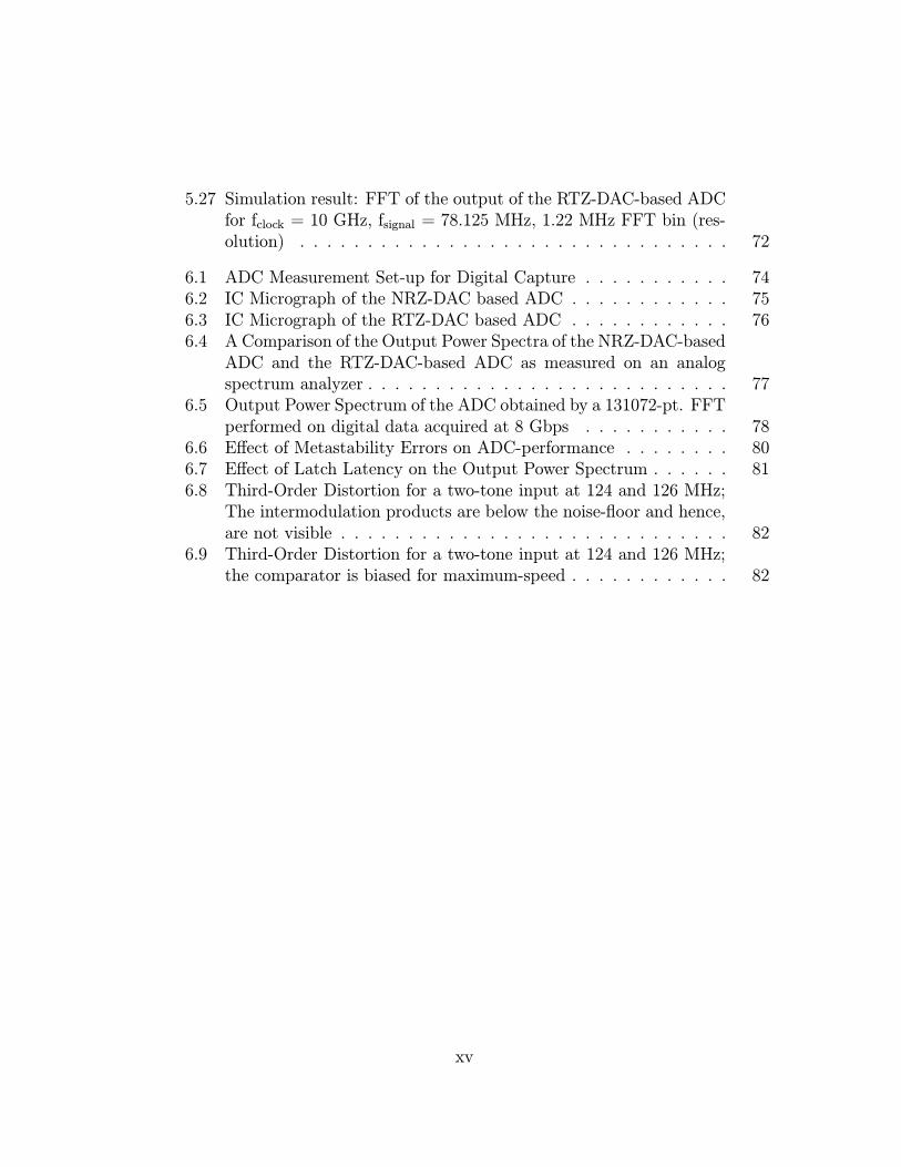
5.27 Simulation result: FFT of the output of the RTZ-DAC-based ADCfor fclock = 10 GHz, fsignal = 78.125 MHz, 1.22 MHz FFT bin (res-olution) . . . . . . . . . . . . . . . . . . . . . . . . . . . . . . . . 72
6.1 ADC Measurement Set-up for Digital Capture . . . . . . . . . . . 746.2 IC Micrograph of the NRZ-DAC based ADC . . . . . . . . . . . . 756.3 IC Micrograph of the RTZ-DAC based ADC . . . . . . . . . . . . 766.4 A Comparison of the Output Power Spectra of the NRZ-DAC-based
ADC and the RTZ-DAC-based ADC as measured on an analogspectrum analyzer . . . . . . . . . . . . . . . . . . . . . . . . . . . 77
6.5 Output Power Spectrum of the ADC obtained by a 131072-pt. FFTperformed on digital data acquired at 8 Gbps . . . . . . . . . . . 78
6.6 Effect of Metastability Errors on ADC-performance . . . . . . . . 806.7 Effect of Latch Latency on the Output Power Spectrum . . . . . . 816.8 Third-Order Distortion for a two-tone input at 124 and 126 MHz;
The intermodulation products are below the noise-floor and hence,are not visible . . . . . . . . . . . . . . . . . . . . . . . . . . . . . 82
6.9 Third-Order Distortion for a two-tone input at 124 and 126 MHz;the comparator is biased for maximum-speed . . . . . . . . . . . . 82
xv

Chapter 1
Introduction
This work describes the design of a 2nd order continuous-time Σ−∆ analog-to-
digital converter (ADC) clocked at 8 GHz and the development of an integrated
circuit (IC) process technology that can support such large scales of integration
together with the required transistor speed and breakdown voltages.
High resolution ADCs are required to increase the bandwidth and frequency
agility of military radar and communication systems. A class of ADCs that achieve
high resolution using oversampling techniques are the Σ−∆ ADCs [30]. These
circuits are particularly attractive in fine-line, very large scale integration (VLSI)
technology because they can trade resolution in time for resolution in bandwidth
in such a way that imprecise analog circuits can be tolerated. The use of high-
frequency modulation and demodulation eliminates the need for abrupt cutoffs in
the anti-aliasing filter at the input to the ADC. To obtain high resolution with
oversampling converters, the clock frequency must be well in excess (102 : 1) of the
signal bandwidth. In order to avoid metastability errors in latched comparators
driven by small input signals, the circuit time constants must be much smaller than
the time period of the clock signal employed. High resolution ADCs consequently
require transistor bandwidths 104 : 1 larger than the signal frequencies involved.
1

CHAPTER 1. Introduction
Transistors with several hundred GHz fτ and fmax are hence required to enable
high-resolution microwave mixed-signal ICs.
1.1 Transistor technologies for mixed-signal ap-
plications
Due to their respective advantages, III-V Heterojunction Bipolar Transistors
(HBTs) and Si/SiGe HBTs are primarily used in high-speed digital and mixed-
signal applications. The principal advantage of III-V InP-based HBTs is superior
bandwidth. There are several factors that contribute to this. For HBTs grown on
GaAs or InP substrates, available lattice-matched materials allow use of an emit-
ter whose bandgap energy is much larger than that of the base. This allows the
base doping to be increased to the limits of incorporation in growth (1020 /cm3),
and results in very low base sheet resistance. High electron velocities are a second
significant advantage of III-V HBTs. Best reported results of InP-based HBTs
include 300 GHz fτ and fmax [9], and 341 GHz fτ [15] while Si/SiGe HBTs have
obtained 210 GHz fτ [19]. Despite the advantages of III-V HBTs provided by
superior material properties, Si/SiGe HBTs remain highly competitive. The high
bandwidths of Si/SiGe HBTs arise in part from aggressive submicron scaling. In
devices with a 0.12µm base-emitter junction, 207 GHz fτ and 285 GHz fmax have
been obtained [17]. Self-aligned polysilicon contacts reduce both the parasitic
collector-base capacitance and the base resistance. In marked contrast to the ag-
gressive submicron scaling and aggressive parasitic reduction employed in Si/SiGe
HBTs, III-V HBTs are typically fabricated with 1−2µm emitter junction widths.Deep submicron scaling will improve the bandwidth of III-V heterojunction tran-
sistors and is critical to their continued success. At UCSB, we have developed one
such process that employs a substrate transfer step to allow independent defini-
tion of the emitter and collector stripes on either side of the base epitaxial layer.
2

CHAPTER 1. Introduction
This process is discussed in the following section.
1.2 HBTs by substrate transfer
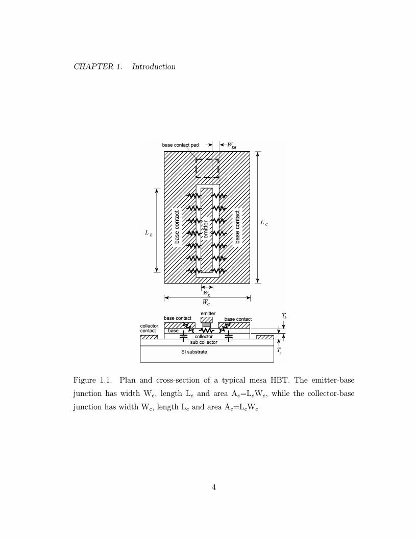
In conventional III-V mesa HBTs (Fig. 1.1), the collector-base junction dimen-
sions must be substantially larger than the emitter dimensions. At the sides of the
emitter stripe, the base ohmic contact must be at least one ohmic contact trans-
fer length, Lcontact, in order to obtain low contact lateral access resistance. In an
InGaAs HBT with 400A base thickness, 5×10¹⁹ /cm3 doping and Ti/Pt/Au met-
alization, Lcontact = 0.4 µm. Lithographic alignment tolerances between emitter
and base also constrain the minimum collector-base junction dimensions. De-
pendent upon the minimum feature size and the length of the emitter stripe,
the base-contact area can contribute as much as 50% of the total collector-base
capacitance. The transferred-substrate HBT achieves a dramatic reduction in
excess collector-base capacitance by employing a substrate transfer step which
allows fabrication of HBTs with submicron emitter-base and collector-base junc-
tions lying on opposing sides of the base epitaxial layer. With this device, fmax
increases rapidly with scaling. A detailed discussion of the process is available
elsewhere [29]. Here, we consider only the results and the shortcomings of these
devices.
With transferred-substrate HBTs, 1.1 THz extrapolated power-gain cutoff fre-
quency [24] and 295 GHz current-gain cutoff frequency [2] have been obtained.
The devices use an InAlAs wide-bandgap emitter and InGaAs narrow-bandgap
base and collector. For the remainder of this thesis, a device with a layer struc-
ture of this kind, with only the emitter-base junction being a heterojunction, will
be referred to as a single heterojunction bipolar transistor (SHBT). Transferred-
substrate SHBTs, by virtue of their narrow-bandgap InGaAs collector, suffer from
low breakdown voltage(Vbr,ceo). The typical Vbr,ceo for a device with a 2000A collec-
3
CHAPTER 1. Introduction
Figure 1.1. Plan and cross-section of a typical mesa HBT. The emitter-base
junction has width We, length Le and area Ae=LeWe, while the collector-base
junction has width Wc, length Lc and area Ac=LcWc
4

CHAPTER 1. Introduction
tor is 1.3 V. Two classes of circuits where this might be a serious impediment are
power amplifiers and digital logic. The effect of Vbr on power amplifiers is obvious
and will not be elaborated here. The logic-speed of a technology is determined by
delays arising from finite transit-times and parasitic capacitances in the transis-
tors. One of the dominant delay terms in logic circuits is given by Ccb×∆Vlogic/Icwhere Ccb, ∆Vlogic and Ic are the collector-base capacitance, the logic swing and
the collector current, respectively [28]. The current density in HBTs is limited by
collector space-charge screening (the Kirk effect [21]) and the maximum current
density before base pushout is Ic,max ∝ Ae/T2c where Ae and Tc are the emitterjunction area and the thickness of the collector respectively. The delay terms
associated with charging the collector-base capacitance are hence minimized by
use of thin collector layers. The low breakdown field of InGaAs makes this an
extremely difficult proposition in SHBTs. A device with a wide-bandgap collector
is, therefore, necessary.
Devices that employ a layer structure of this kind, with both the emitter-base
and collector-base junctions being heterojunctions, are called double heterojunc-
tion bipolar transistors (DHBTs). Chapter 2 of this thesis is devoted to a detailed
discussion of the development of DHBTs by substrate transfer.
1.3 Narrow-mesa HBTs
A number of high-speed analog ICs have been fabricated in the transferred-
substrate HBT process. Among these are 80 GHz distributed amplifiers [22],
broadband Darlington and fτ doubler resistive feedback amplifiers [23]. Tuned
mm-wave amplifiers have also been demonstrated in this process, including 75 GHz
power-amplifiers [11] and 175-GHz small-signal, tuned-amplifiers [36]. Efforts at
large scale integration have not been as successful, though. Σ−∆ ADCs [16] and2-bit adders [26] have been fabricated, but success in each case was preceded by a
5
CHAPTER 1. Introduction
very large number of failed process-runs. Initial attempts in this project were still
aimed at fabricating the Σ−∆ ADC in a substrate-transfer process, considering
its superior performance relative to a mesa-process, but after a year of fruitless
labor, it was decided to forego the transferred-substrate process in favor of the
more manufacturable mesa-process.
To ease process development, most of the features of the transferred-substrate
process, including the microstrip wiring environment, were retained. The base
ohmic contact, at the sides of the emitter stripe, was narrowed down to one ohmic
contact transfer length, Lcontact, to minimize the collector-base capacitance while
maintaining a low contact resistance. The features of this narrow-mesa process,
and the device results are discussed in Chapter 3.
1.4 Σ−∆ ADC Design
The first generation Σ−∆ ADC at UCSB was designed by S. Jaganathan [18].The design had 150 transistors, was clocked at 18 GHz, and was fabricated in the
transferred-substrate SHBT technology. No noise-shaping was observed below
1 GHz and was attributed to metastability-errors in the quantizer. Our initial
designs address this problem. Along with an additional stage of regeneration,
the ADC also has a Cherry-Hooper [5] based pre-amplifier to the quantizer, to
minimize metastability errors. The design has 130 transistors, is clocked at 20
GHz, and uses the transferred-substrate DHBT process. Following a series of
failed process-runs, spread over a period of twelve months, it was decided to shelve
the transferred-substrate process for a more manufacturable mesa process. This
design was, hence, never successfully fabricated. During the twelve month period
between our first and second generation designs, the problem of excess delay was
considered. The additional stage of regeneration in the comparator was found
to change the location of the centroid of the digital-to-analog converter(DAC)
6
CHAPTER 1. Introduction
current-pulse degrading the signal-to-noise ratio (SNR). The loss in SNR could
hence be retrieved by moving the centroid-in-time of the DAC current-pulse back
to its original location. This was achieved by using a Return-to-Zero(RTZ) DAC.
The second generation mask-set has two versions of the Σ−∆ ADC. The
first version uses a Non-return-to-zero (NRZ) DAC while the second version has
an RTZ DAC. These designs also use a 10 GHz clock to minimize metastability
errors in the quantizer. To test the validity of the comparator layout, a static
frequency divider is also included in this mask-set.
Chapter 4 of the thesis presents our analysis on the problems of metastabil-
ity and excess delay in the loop, the subsequent simulations, and our inferences
based on the simulation-results. The measured results of the ADC and the static
frequency divider are discussed in Chapter 5. Conclusions based on the measured
results are drawn and future directions suggested in Chapter 6.
7

Chapter 2
DHBTs by substrate-transfer
2.1 SHBT (vs) DHBT
In order to better explain the development of DHBTs by substrate-transfer,
it is necessary to first trace the history of the transferred-substrate SHBT. The
first transferred-substrate SHBT was demonstrated in 1996 [1]. Since then, a
number of graduate students have worked on the transferred-substrate SHBT
making medium scales of integration (MSI) possible [28, 18]. For this reason,
the DHBT process is tailored along the lines of the SHBT process to the extent
possible. Here, we discuss only the variations in the layer structure, the reasons for
these differences, and the associated changes in the process. A detailed discussion
of the transferred-substrate SHBT epitaxial layer structure and process can be
found in D. Mensa’s Ph. D. thesis [29].
Two disadvantages of the transferred-substrate SHBT are high thermal resis-
tance and low breakdown voltage. All transferred-substrate SHBTs fabricated
to date use InAlAs emitter layers and InGaAs base and collector layers. In a
transferred-substrate HBT, the heat flows through the emitter and hence, its
thermal resistance is dominated by the temperature gradients arising from the
8

CHAPTER 2. DHBTs by substrate-transfer
low thermal conductivity of the InAlAs (9.9 W/mK) and InGaAs (4.8 W/mK)
layers. The reasons for the poor breakdown voltage of the transferred-substrate
SHBT and the need for larger breakdown voltage have already been elaborated in
chapter 1. InP, with its high thermal-conductivity (68 W/mK) and large bandgap,
will alleviate both problems. While use of high-thermal-conductivity InP emit-
ter and collector epitaxial layers will greatly increase allowable power per unit
HBT junction area, the large breakdown field of InP (30V/µm) will increase the
breakdown voltage of the HBT.
2.1.1 Variations in Epitaxial Layer Structure
The InP emitter and collector epitaxial layers necessitate new designs for the
base-emitter and base-collector interfacial grades. The conduction band edge
discontinuities (∆Ec) at the heterointerfaces are removed by providing a lin-
ear bandgap variation for the interfacial region using a chirped super lattice
(CSL) [31]. Such a grade results in a quasi-electric field and is neutralized by
creating an equal and opposite field using a dipole. A delta-doped layer at the
collector-end of the base-collector grade in association with the heavily-doped In-
GaAs base forms this dipole. The period of the superlattice for the base-collector
grade is 1.5 nm, and not any wider, to avoid resonant behavior in the mini-
bands [31]. From a material growth perspective, the InP/InGaAs CSL is much
more difficult to grow than the InAlAs/InGaAs CSL due to the interfacial strain
that builds up as a result of intermixing of Group-V elements at the interface [37].
For this reason, all-arsenide (InAlAs/InGaAs) CSLs are used to grade all the
heterointerfaces.
The other change in the layer structure involves substrate-transfer. HBTs by
substrate-transfer involve a processing step where the original InP substrate is
completely etched away. If an etch-stop layer is not present between the substrate
and the InP collector layer, the collector will also be etched away in the process.
9
CHAPTER 2. DHBTs by substrate-transfer
Table 2.1. DHBT layer structureMaterial Doping(cm−3) Thickness(nm)n-InGaAs 1 · 1019 100n-InGaAlAs 1 · 1019 20n-InP 1 · 1019 90n-InP 8 · 1017 30
n-InGaAlAs 8 · 1017 23.3n-InGaAlAs 2 · 1018 6.6p-InGaAs 4 · 1019 40n-InAlGaAs 1 · 1016 48n-InP 2 · 1018 2n-InP 1 · 1016 250
n-InGaAs 1 · 1019 75InGaAs UID 150InAlAs UID 250
We use a 1500A thick InGaAs layer as the etch-stop layer. The layer structure is
shown in Table 3.1 and the band diagram at a bias of Vce=1.2 V and Vbe=0.7 V
is shown in Fig. 2.1.
2.1.2 Process Development
To obtain a reproducible, and minimum-undercut, junction-profile while main-
taining a smooth surface, the transferred-substrate SHBT process uses a com-
bination of an RIE-based dry etch and selective wet-etch chemistry to define
the base-emitter junction. The dry-etch is CH4/Ar/H2-based while a HCl-based
solution is used for the wet-etch. We tried modifying this process to suit the
DHBT layer-structure, where the emitter is InP rather than InAlAs, but the
post-dry-etch surface was very rough and this roughness resulted in large vari-
ations in the undercut-profile of the base-emitter junction after the subsequent
wet-etch. In addition to CH4/Ar/H2-based dry etching, we also tried Cl-based
dry etching, but were unable to obtain any uniformity in the undercut-profile.
10
CHAPTER 2. DHBTs by substrate-transfer
Figure 2.1. Band diagram, under bias, of a typical device: Vce=1.2 V and Vbe=0.7
V
As a result, an all wet-etch process is used to define the base-emitter junction.
The emitter-cap (InGaAs) and the emitter-cap grade (InAlGaAs) are etched in
a dilute H2O2/H3PO4/H2O solution (relative concentration of 1:1:25) while the
emitter(InP) is etched in a solution of HCl diluted with H3PO4(relative con-
centration of 1:4). Since HCl-based etchants show great selectivity in etch-rates
between InAlAs and InGaAs, this etch stops in the base-emitter grade. A citric
acid based solution (citric:H2O:H2O2:H3PO4 ; 55:220:5:1) is used to etch the re-
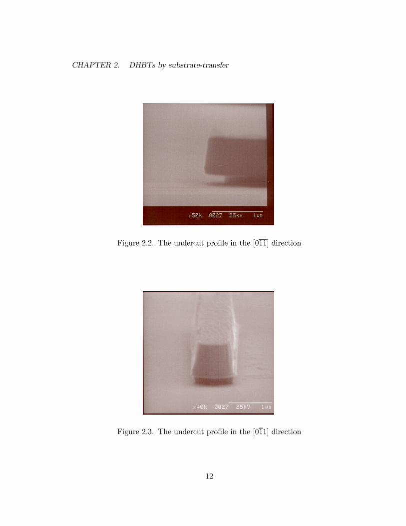
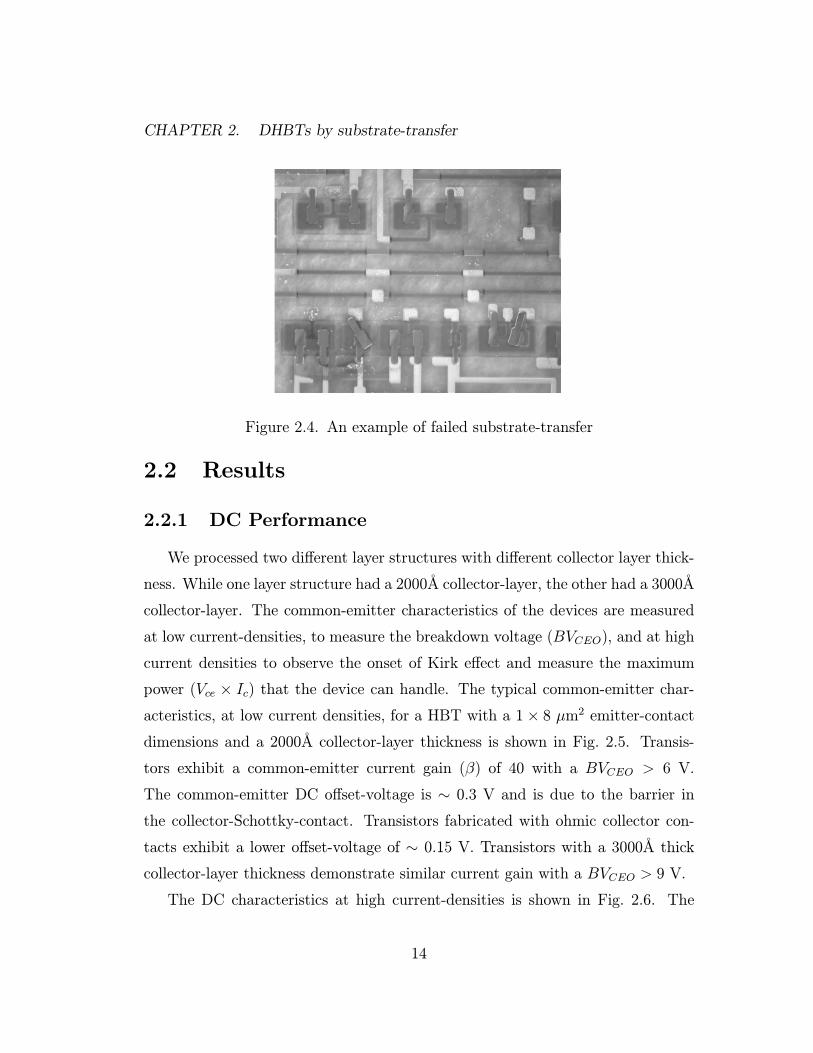
maining base-emitter grade and into the base epitaxial layer. Figs. 2.2 and 2.3
show the undercut-profile along the [011] and the [011] directions, respectively.
The undercut along the [011] direction is large (0.5µm). A better process is nec-
essary to improve the yield on HBTs with short emitter-stripes. At this time, we
are limited to a minimum emitter-stripe length of 6µm.
In the transferred-substrate process, prior to the substrate-removal etch, the
‘processed’ InP-wafer is solder-bonded to a GaAs carrier wafer. The original InP
11
CHAPTER 2. DHBTs by substrate-transfer
Figure 2.2. The undercut profile in the [011] direction
Figure 2.3. The undercut profile in the [011] direction
12

CHAPTER 2. DHBTs by substrate-transfer
substrate is then completely etched in a HCl-based etch. Transferred-substrate
SHBTs employ an InGaAs collector and this acts as an excellent etch-stop layer
for the HCl-based substrate-removal etch. Based on this knowledge, we felt that
it would suffice if the transistor mesa, and hence the InP collector-epitaxial-layer,
is screened by an InGaAs layer during the substrate-removal etch. The mesa-
isolation etch was modified in such a way that the transistor-mesa was protected
by a thick layer of InGaAs (1500A). Since GaAs has a larger co-efficient of thermal
expansion (CTE) than InP, the latter would be under net biaxial compression upon
cooling. In this configuration, the free surface of the InP would be under tension,
which would create the risk of crack-initiation [12]. To avoid increasing the risk of
crack-initiation further, we were, at that time, averse to leaving a continuous film
of InGaAs on the wafer. The result of such an approach at substrate-transfer for
DHBTs is shown in Fig. 2.4. On the figure, one can see that some of the base-
mesas have been attacked during the substrate-removal etch. The InP collector
has been removed in these mesas and hence, the InGaAs etch-stop layer is free to
float around. Also, the surface is found to be spotty with pieces of semiconductor.
At this point, we were left with no option but to modify the isolation-etch in
such a way that a continuous film of InGaAs screened the InP collector from the
substrate-removal etch. The InP collector is still removed in places and this is
attributed to cracks in the InGaAs arising from the difference in CTE between
InP and GaAs. We have been able to improve the yield further using multiple
etch-stop layers and using an AlN carrier-wafer that is better matched in CTE
(than GaAs) to the original InP substrate. In spite of these improvements, the
fraction of attacked-mesas (1 in 200) is still large enough to seriously impede the
development of medium scale integration ICs in this technology.
13
CHAPTER 2. DHBTs by substrate-transfer
Figure 2.4. An example of failed substrate-transfer
2.2 Results
2.2.1 DC Performance
We processed two different layer structures with different collector layer thick-
ness. While one layer structure had a 2000A collector-layer, the other had a 3000A
collector-layer. The common-emitter characteristics of the devices are measured
at low current-densities, to measure the breakdown voltage (BVCEO), and at high
current densities to observe the onset of Kirk effect and measure the maximum
power (Vce × Ic) that the device can handle. The typical common-emitter char-acteristics, at low current densities, for a HBT with a 1× 8 µm2 emitter-contactdimensions and a 2000A collector-layer thickness is shown in Fig. 2.5. Transis-
tors exhibit a common-emitter current gain (β) of 40 with a BVCEO > 6 V.
The common-emitter DC offset-voltage is ∼ 0.3 V and is due to the barrier in
the collector-Schottky-contact. Transistors fabricated with ohmic collector con-
tacts exhibit a lower offset-voltage of ∼ 0.15 V. Transistors with a 3000A thickcollector-layer thickness demonstrate similar current gain with a BVCEO > 9 V.
The DC characteristics at high current-densities is shown in Fig. 2.6. The
14

CHAPTER 2. DHBTs by substrate-transfer
0
5000
1 104
1.5 104
2 104
2.5 104
0 1 2 3 4 5 6 7
J c (A/c
m2 )
Vce
(volts)
Figure 2.5. Ic-Vce characteristics at low current-densities, IB is in steps of 15 µA
maximum power density before device-failure, for HBTs with a 2000A collector-
layer, is 4·105W/cm 2. For devices with 3000A collector-depletion-layer thickness,
the maximum power density is 6·105W/cm 2. The Vce,sat at a current density, J, of
1·105 A/cm2 is 1 V. The Vce,sat at high current-densities is determined by the onsetof base pushout (the Kirk effect). Calculations, assuming a layer-structure such
as the one that was processed, show that the Vce,sat at a current-density of 1 · 105A/cm2, should be 0.7 V. On this particular process-run, there was considerable
misalignment between the collector and emitter stripes, resulting in additional
collector space-charge resistance and hence, increased Vce,sat for a given current
density.
2.2.2 Microwave performance
The devices were characterized by measuring the S-parameters using a 75-110
GHz network analyzer. To avoid uncorrectable measurement errors arising from
variable probe-probe electromagnetic coupling, the HBTs are separated from their
probe pads by long, on-wafer, 50-ohm microstrip lines. On-wafer line-reflect-line
15

CHAPTER 2. DHBTs by substrate-transfer
0
2 104
4 104
6 104
8 104
1 105
0 1 2 3 4 5
J c (A/c
m2 )
Vce
(volts)
Figure 2.6. Ic-Vce characteristics at high current-densities, IB is in steps of 50µA
Table 2.2. Microwave performanceCollector thickness Vce(V ) J (A/cm2) fτ (GHz) fmax(GHz)
2000A 1.5 1 · 105 215 210
3000A 2.5 9 · 104 165 300
calibration standards are used to de-embed the transistor S-parameters [24]. The
current gain (h21) and the power gain (U) are extrapolated at -20 dB/decade
to obtain the two figures of merit, the current-gain cutoff frequency, fτ , and the
maximum frequency of oscillation, fmax, respectively. Transistor-gains are plotted
in Figs. 2.7 and 2.8 for the two layer structures.
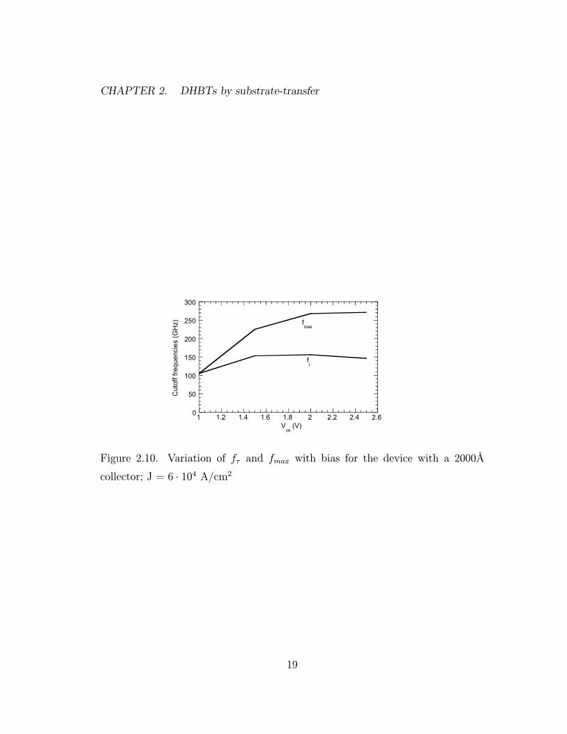
Table 2.2 compares the microwave performance of the two layer structures.
While the device with a 3000A thick collector exhibits a high fmax of 300 GHz,
the device with a 2000A thick collector offers a better balance between fτ and
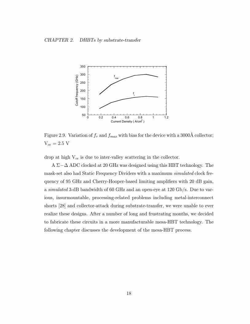
fmax. The variation of fτ and fmax with bias for the device with the 3000A
collector-layer is shown in Figs. 2.9 and 2.10. The Vce is maintained at 2.5 V for
the first plot and J is maintained at 6 · 104 A/cm2 for the second plot. The dropin the cutoff frequencies at high current densities is due to the Kirk effect. The
16

CHAPTER 2. DHBTs by substrate-transfer
0
5
10
15
20
10 100
Gai
n (d
B)
frequency (GHz)
h21
U
20 dB/decade
Figure 2.7. RF gains for a device a 1× 8µm2 emitter contact. This device has a
400A thick graded base and a 3000A thick collector-depletion-region
0
5
10
15
20
10 100
Gai
n (d
B)
Frequency (GHz)
h21
U
20 dB/decade
Figure 2.8. RF gains for a device a 1× 8µm2 emitter contact. This device has a
400A thick graded base and a 2000A thick collector-depletion-region
17
CHAPTER 2. DHBTs by substrate-transfer
50
100
150
200
250
300
350
0 0.2 0.4 0.6 0.8 1 1.2
Cut
off f
requ
ency
(GH
z)
Current Density ( A/cm2 )
ft
fmax
Figure 2.9. Variation of fτ and fmax with bias for the device with a 3000A collector;
Vce = 2.5 V
drop at high Vce is due to inter-valley scattering in the collector.
A Σ−∆ ADC clocked at 20 GHz was designed using this HBT technology. Themask-set also had Static Frequency Dividers with a maximum simulated clock fre-
quency of 95 GHz and Cherry-Hooper-based limiting amplifiers with 20 dB gain,
a simulated 3-dB bandwidth of 60 GHz and an open-eye at 120 Gb/s. Due to var-
ious, insurmountable, processing-related problems including metal-interconnect
shorts [28] and collector-attack during substrate-transfer, we were unable to ever
realize these designs. After a number of long and frustrating months, we decided
to fabricate these circuits in a more manufacturable mesa-HBT technology. The
following chapter discusses the development of the mesa-HBT process.
18
CHAPTER 2. DHBTs by substrate-transfer
0
50
100
150
200
250
300
1 1.2 1.4 1.6 1.8 2 2.2 2.4 2.6
Cut
off f
requ
enci
es (G
Hz)
Vce
(V)
fmax
ft
Figure 2.10. Variation of fτ and fmax with bias for the device with a 2000A
collector; J = 6 · 104 A/cm2
19

Chapter 3
Narrow-mesa HBTs
The shortcomings of the transferred-substrate process, when used to achieve
medium scales of integration, are first considered. Following this, we explain
how a mesa-process eliminates these problems. The features of the mesa-process
are then discussed. Following this, the device and circuit results are presented.
3.1 Realizing Medium Scale Integration ICs
The process-related problems in fabricating medium scale integration(MSI)
ICs in the transferred-substrate DHBT process can be broadly classified into two
categories; problems related to substrate-transfer and problems related to medium
scale integration. The former has been discussed at length in chapter 2 and is read-
ily solved by eliminating substrate-transfer (using a mesa-HBT process). Here,
we will limit the discussion to problems related to medium scale integration. One
such yield-limiting mechanism in our process is poor insulation between the two
levels of interconnect metal. In order to understand the causes for this problem, a
brief description of the transferred-substrate process is necessary. Self-aligned base
contacts are deposited on the wafer after the base-emitter junction is defined. The
20

CHAPTER 3. Narrow-mesa HBTs
Figure 3.1. Interconnect-metal profile with an angled evaporation
active devices are then isolated using a wet-etch, and passivated and planarized
in polyimide. A dry etch is used to pattern the polyimide in such a way that
the subsequent level of interconnect metal can make an electrical contact to the
emitter and base metal layers. To provide step-coverage over the polyimide-mesas
(∼ 8000A), the wafer is placed at an angle of 35o during the metal evaporation.The profile of the metal-edge is found to be rough and is shown in Fig. 3.1. Af-
ter the first level of interconnect-metal, a silicon nitride (SiN) dielectric-layer is
deposited and patterned in such a way that this layer acts both as the dielectric
for MIM(metal-insulator-metal) capacitors and as the insulating layer between
the first and second level of interconnects in places where metal-crossovers are
required. Since the heat flows through the emitter in the transferred-substrate
HBTs, proper heat-sinking is required. The second level of interconnect-metal
serves this purpose as well.
A detailed study of the various yield-limiting mechanisms has been attempted
by T. Mathew [28]. We will limit ourselves here to a brief discussion of his con-
21

CHAPTER 3. Narrow-mesa HBTs
clusions, and our subsequent attempts at addressing his concerns. He claimed
that the primary yield-limiting mechanism was lack of insulation between the two
levels of interconnect-metal on top of the device-mesa. Since the second level of
interconnect-metal is used as a heat-sink for the HBTs, this results in a grounded-
emitter. He was unable to find the cause for this problem, though, because none
of his test-structures showed sufficient instances of interconnect-metal shorts to
explain its large occurence on device-mesas. Based on the assumption that this
problem was arising due to poor coverage of SiN over the spikes in the interconnect-
metal, we made two changes to the process. The angled evaporation of metal-1
was first shelved in favor of an evaporation with no angle. Step-coverage was
achieved by increasing the thickness of the interconnect-metal. A much smoother
metal-profile, with good step-coverage over polyimide, was achieved and is shown
in Fig. 3.2. However, the effect of this on interconnect-metal shorts was not as
profound. We noticed very little decrease in the frequency of interconnect-metal
shorts with this process-modification. In addition to this, we also tried blanket-
evaporating a 500A SiO2 insulating layer before depositing SiN. This insulating
SiO2 layer was very effective in mitigating the interconnect-shorts problem and re-
duced the frequency of its occurence by ∼ 25%. In spite of these changes, and theassociated improvement in yield, the frequency of interconnect-metal shorts was
large enough to severely impede the development of MSI ICs in the transferred-
substrate process. For this reason, we were left with no alternative but to fabricate
the circuits in a more manufacturable mesa-HBT process that avoided these prob-
lems.
In a mesa-HBT, the heat flows through the substrate and hence, no heat-
sinking is required. Consequently, the second level of metal-interconnect is not
required on top of the device-mesas. In order to completely eliminate the problem
of metal-interconnect shorts, crossovers between the interconnect metals with SiN
as the insulating layer are also avoided. All crossovers are achieved by using the
22

CHAPTER 3. Narrow-mesa HBTs
Figure 3.2. Interconnect-metal profile with a non-angled evaporation
collector metal as a level of interconnect, with polyimide as the insulating layer.
With these modifications, interconnect-metal shorts have ceased to be an yield
limiting mechanism for MSI ICs. The various process-features of this mesa-HBT
process are discussed in the following section.
3.2 Mesa-HBT Technology: Process Features
Prior to discussing the features of the mesa-HBT technology, we will mention
the two differences in layer structure between the mesa-HBT and transferred-
substrate HBT.The collector contact is ohmic in nature for the mesa-HBT and
hence, a heavily-doped sub-collector layer is required. The need for multiple etch-
stop-layers, in order to reduce the risk of crack-initiation during the substrate-
transfer step, is obviated. The layer structure is shown in Table 3.1.
With the intent of making process-development quick and easy, a conscious
attempt was made to retain the features of the transferred-substrate HBT to the
23

CHAPTER 3. Narrow-mesa HBTs
Table 3.1. Mesa-DHBT layer structureMaterial Doping(cm−3) Thickness(nm)n-InGaAs 1 · 1019 30n-InGaAlAs 1 · 1019 9n-InP 1 · 1019 90n-InP 8 · 1017 30
n-InGaAlAs 8 · 1017 23.3n-InGaAlAs 2 · 1018 6.6p-InGaAs 4 · 1019 40n-InGaAs 2.25 · 1016 10n-InAlGaAs 2.25 · 1016 24n-InP 5.66 · 1018 3n-InP 2.25 · 1016 163
n-InGaAs 1 · 1019 25n-InP 1 · 1019 125InGaAs UID 5InAlAs UID 25InP UID 50
greatest extent possible. The mesa-HBT process is indistinguishable from the
transferred-substrate HBT until the deposition of the base-contact. The next
level of metal-deposition makes a pillar-like contact to the base metal in such
a way that the subsequent polyimide-planarization etch simultaneously exposes
both the emitter and base contacts. The base-collector junction is then defined
using selective-wet-etch chemistry similar to the etch used to define the base-
emitter junction. This etch leaves the sub-collector layer exposed and collector
contacts can be deposited. An SEM micrograph of the device, and a cross-section
of the HBT, after collector metal deposition are shown in Figs. 3.3 and 3.4. The
collector metal is also used as a level of interconnect.
The active junctions are then passivated and planarized in polyimide. The
polyimide is patterned in such a way that the first level of interconnect-metal
can make electrical contacts to the three terminals of the transistor. Following
24

CHAPTER 3. Narrow-mesa HBTs
Figure 3.3. SEM micrograph of a mesa-HBT
Emitter-contact Base Plug
Base-contactCollector-contact
InGaAs base
InP emitter
InGaAs base
InP collector
Figure 3.4. Cross-section of a mesa-HBT
25

CHAPTER 3. Narrow-mesa HBTs
this, thin-film NiCr resistors are deposited. The typical sheet resistance is 40 Ω/sq.
The ensuing level of interconnect-metal makes electrical contacts to the transistors
and the resistors and is also used for most interconnects. As mentioned earlier,
all interconnect-crossovers are achieved using collector metal with polyimide as
the insulating dielectric. Following the first level of metal-interconnect, a 4000A
SiN dielectric-layer is deposited and is followed by the second level of interconnect
metal. The second level of interconnect metal is a misnomer since it is used only as
the second-plate for the MIM capacitors. Since we are worried about interconnect-
metal shorts, we avoid using the second level of metal for any interconnects. With
proper process-development, it should be possible to use this layer of metal for
interconnects also.
To realize complex mixed-signal ICs, a wiring environment that maintains
control of signal integrity and has predictable characteristics to enable robust
computer-aided design (CAD) is required. Thin-film-dielectric microstrip-wiring
provides controlled-impedance interconnects within dense mixed-signal ICs. The
associated ground plane eliminates signal coupling through on-wafer ground-return
inductance. Such a wiring environment is added to the process with the addition
of a dielectric layer and ground-plane above the IC top-surface wiring planes. We
implement this by spin-casting a 5µm thick benzocyclobutene (BCB) polymer
film, etching vias in BCB and depositing the top ground-plane by electroplating.
Figs. 3.5 and 3.6 show a cross-sectional view of the wiring environment, and an
IC micrograph of a master-slave latch after ground-plane plating, respectively.
In such a wiring environment, 8-micron and 3-micron width conductors have
controlled 50Ω and 80Ω impedances respectively. Since the dielectric is thin,
ground-via inductance is greatly reduced. Interconnects are not significantly cou-
pled for line spacings greater than 10µm. Ground-vias can be closely spaced, as
is required in complex ICs. The disadvantage of using a thin dielectric is the
increase in skin-loss compared to a conventional microstrip of similar impedance.
26

CHAPTER 3. Narrow-mesa HBTs
Figure 3.5. Cross-sectional view of the microstrip wiring environment
Figure 3.6. Master-slave latch after plating the ground-plane
27
In addition, the ground-plane reduces line impedances and increases capacitance,
thereby increasing node-charging times on unterminated interconnects. We have
successfully fabricated mixed-signal ICs with moderate complexity (80 transis-
tors) using this technology. More complex ICs (100-150 transistors) are currently
being designed.
3.3 Mesa-HBT Results
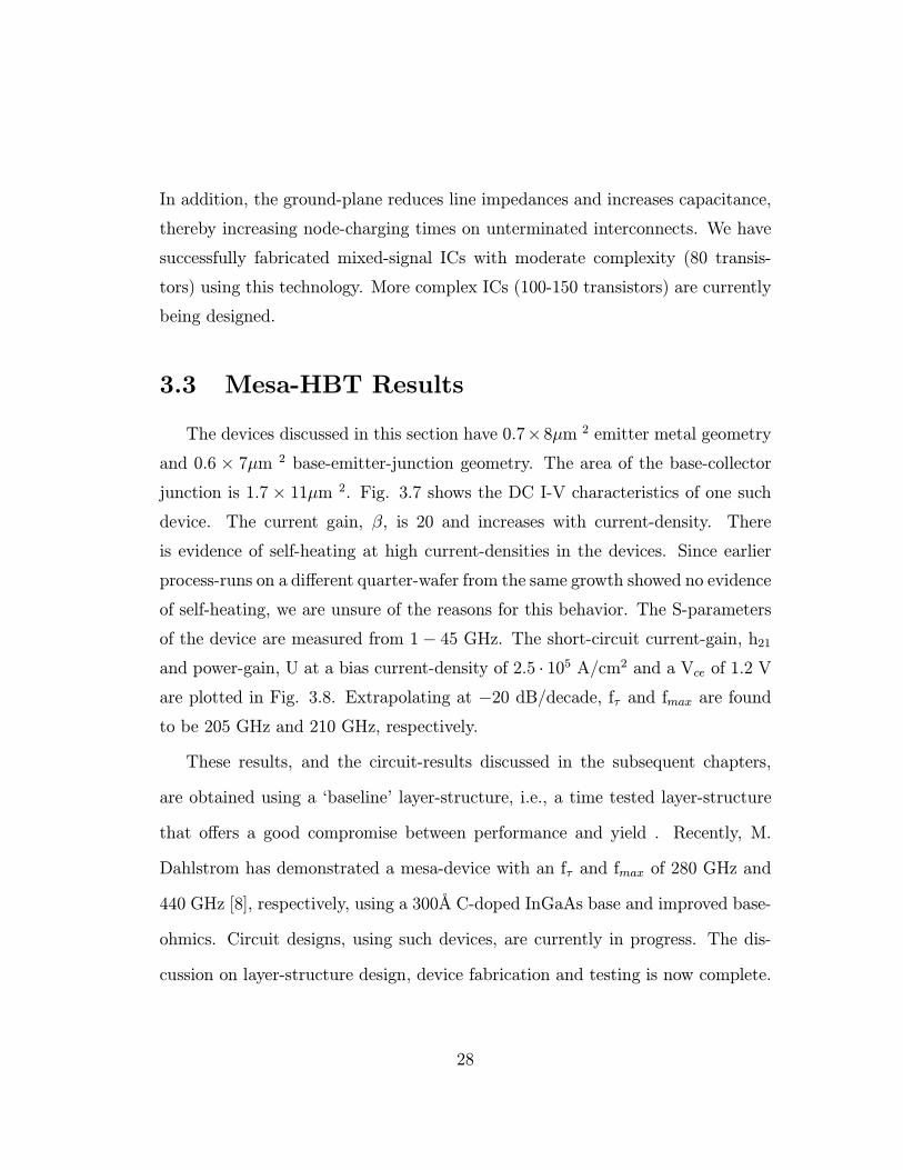
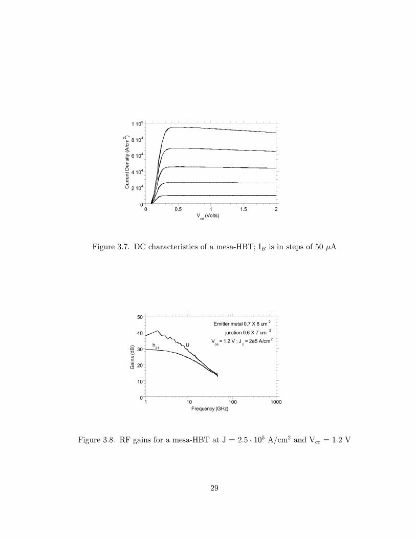
The devices discussed in this section have 0.7×8µm 2 emitter metal geometry
and 0.6 × 7µm 2 base-emitter-junction geometry. The area of the base-collector
junction is 1.7 × 11µm 2. Fig. 3.7 shows the DC I-V characteristics of one such
device. The current gain, β, is 20 and increases with current-density. There
is evidence of self-heating at high current-densities in the devices. Since earlier
process-runs on a different quarter-wafer from the same growth showed no evidence
of self-heating, we are unsure of the reasons for this behavior. The S-parameters
of the device are measured from 1− 45 GHz. The short-circuit current-gain, h21and power-gain, U at a bias current-density of 2.5 · 105 A/cm2 and a Vce of 1.2 Vare plotted in Fig. 3.8. Extrapolating at −20 dB/decade, fτ and fmax are foundto be 205 GHz and 210 GHz, respectively.
These results, and the circuit-results discussed in the subsequent chapters,
are obtained using a ‘baseline’ layer-structure, i.e., a time tested layer-structure
that offers a good compromise between performance and yield . Recently, M.
Dahlstrom has demonstrated a mesa-device with an fτ and fmax of 280 GHz and
440 GHz [8], respectively, using a 300A C-doped InGaAs base and improved base-
ohmics. Circuit designs, using such devices, are currently in progress. The dis-
cussion on layer-structure design, device fabrication and testing is now complete.
28
0
2 104
4 104
6 104
8 104
1 105
0 0.5 1 1.5 2
Cur
rent
Den
sity
(A/c
m2 )
Vce
(Volts)
Figure 3.7. DC characteristics of a mesa-HBT; IB is in steps of 50 µA
0
10
20
30
40
50
1 10 100 1000
Gai
ns (d
B)
Frequency (GHz)
h21
U
Emitter metal 0.7 X 8 um 2
junction 0.6 X 7 um 2
Vce
= 1.2 V ; Jc = 2e5 A/cm2
Figure 3.8. RF gains for a mesa-HBT at J = 2.5 · 105 A/cm2 and Vce = 1.2 V
29

We will now present the results of a static frequency divider fabricated in the
mesa-HBT technology. The static frequency divider is measured in the 4-40 GHz,
50-75 GHz and 75-100 GHz frequency-ranges. The following section discusses the
measurement-setup for each frequency range and the respective measurements.
3.4 Static Frequency Divider
Fully-static frequency dividers are used as benchmarks to evaluate the speed of
a digital technology because of the universal presence of master-slave flip-flops in
synchronous digital circuits. Impressive results, measured by the maximum clock
frequency of the divider, have been reported in SiGe [32] and InAlAs/InGaAs HBT
Technologies [35, 27]. The circuit schematic (Fig. 3.9) is similar to the 66-GHz
static frequency divider reported by Lee et al [25]. A simple differential-pair is
used as the output buffer. A detailed analysis of the various delay terms associated
with a ECL-based divider can be found in [28]. To minimize the number of active
devices, we do not use a current-mirror based biasing scheme here. Instead, the
bias currents are established using resistors.
At low frequencies, a 10 MHz-40 GHz frequency synthesizer output directly
drives the clock input (Fig. 3.10). A low frequency measurement was performed(Fig. 3.11)
to establish the fully-static nature of the divider.
For 50 GHz-75 GHz measurements, the 10 MHz-40 GHz synthesizer drives
a frequency tripler (with output frequency range between 50 and 75 GHz) with
output delivered on-wafer with a V-band waveguide-coupled micro-coaxial probe
(Fig. 3.12). Fig. 3.13 shows the output voltage of the divider at 37.5 GHz, corre-
30

!!""
!!""
#$!!%"&'()&()&'()&!()&()%(*%
&' &'&'&'
&'&'&'&'
&
&
&'
&'&'
&'
&! &!
&! &!
&
&&
& &
&&
&
Figure 3.9. Divider : Circuit Schematic
Figure 3.10. Divider Measurement Setup : 4-40 GHz
31
-0.3
-0.25
-0.2
-0.15
-0.1
-0.05
0
22 22.5 23 23.5 24
V out (V
olts
)
time (nsec)
Figure 3.11. Output Voltage at 2 GHz; fclk = 4 GHz
sponding to a 75 GHz input-clock.
For W-band measurements, the synthesizer drives a 75 GHz-110 GHz fre-
quency tripler whose output is then amplified and delivered through a waveguide-
coupled W-band wafer probe (Fig. 3.14). Fig. 3.15 shows the output voltage at
43.5 GHz, corresponding to a 87 GHz input-clock, the maximum clock frequency
of our divider.
The current-switching transistors and the emitter-followers are biased at current-
densities of 2.6·105 A/cm2 and 2.0·105 A/cm2, respectively. The divider dissipates
700 mW of power from a -4.5 V supply. The subsequent chapters in the thesis are
devoted to the design, analysis and testing of ADCs in this mesa technology.
32

Figure 3.12. Divider Measurement Setup : 50-75 GHz
-0.35
-0.3
-0.25
-0.2
-0.15
-0.1
-0.05
0
22 22.02 22.04 22.06 22.08 22.1 22.12 22.14
V out (V
olts
)
time (nsec)
Figure 3.13. Output Voltage at 37.5 GHz; fclk = 75 GHz
33

Figure 3.14. Divider Measurement Setup : 75-110 GHz
-0.2
-0.18
-0.16
-0.14
-0.12
-0.1
-0.08
-0.06
22 22.02 22.04 22.06 22.08 22.1 22.12 22.14
V out (V
olts
)
time (nsec)
Figure 3.15. Output Voltage at 43.5 GHz; fclk = 87 GHz
34

Chapter 4
Σ−∆ ADC Theory
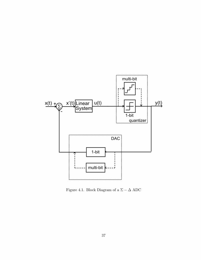
The basic concept underlying Σ−∆ ADCs is the use of feedback to improve
the effective resolution of a coarse quantizer. An internal, low-resolution ADC,
typically 1-bit, is clocked at a frequency that is much larger than the signal-
frequency. Using negative-feedback, the quantization-noise of this internal ADC
is noise-shaped in such a way that the quantization-noise is decreased in the signal-
bandwidth at the cost of increased quantization-noise at higher frequencies.
A block diagram of a Σ−∆ ADC is shown in Fig. 4.1. The linear system in
the forward path of the ADC can either be a low-pass filter or a band-pass filter,
resulting in a baseband or a bandpass ADC, respectively. Here, we will limit our
discussion to baseband ADCs. The order of this filter decides the extent of in-band
noise-suppression obtained. Higher-order filters result in increased suppression of
in-band noise. Third-or-higher order modulators with a 1-bit internal quantizer,
though, offer a strong basis for instability and the circuit might settle into a large-
amplitude, low-frequency, limit cycle. It is very difficult to obtain stability at all
35

input levels for a 3rd or higher-order modulator having a single-bit quantizer [30].
For this reason, we limit our design and discussion to 2nd order modulators.
The performance of the Σ−∆ ADC can also be enhanced by using a multi-bitinternal quantizer. If a multi-bit internal quantizer is used, a multi-bit DAC is
required in the feedback path. As with any feedback system, in the limit of large
loop gain, the closed loop transfer function becomes the reciprocal of the feedback
factor, in this case the DAC. Hence, the ADC resolution can be no greater than
the fractional precision of the feedback DAC. At the target 8-9 bits of resolution,
we cannot obtain such precision in the DAC. Considering these factors, our design
uses a second order low-pass filter and a 1-bit internal quantizer and we will hence,
limit our subsequent discussions to the same.
4.1 Linearized Theory
The easiest way to understand a Σ−∆ ADC is in terms of the frequency-
domain description of an approximate linearized model. In this model, a non-
linear operation, quantization, is replaced by the addition of a noise signal. Specif-
ically, the output, y(t), is written as
y(t) = u(t) + e(t) (4.1)
It is then approximated that e(t) is statistically independent of u(t), an approx-
imation which becomes increasingly less accurate as the resolution of the quan-
tizer decreases. Linear System theory is then invoked to show that the output
of the modulator is the sum of the filtered input signal, X(jω), and the filtered
36
+!",-
-./0./ 1
*
02./ ./
*3
*3
45#
*3
*3
6"!7
Figure 4.1. Block Diagram of a Σ−∆ ADC
37
8. / 9. / 92. / :. /
;. /
1 11
<. /
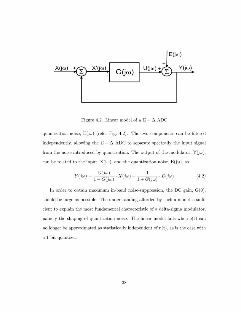
*
Figure 4.2. Linear model of a Σ−∆ ADC
quantization noise, E(jω) (refer Fig. 4.2). The two components can be filtered
independently, allowing the Σ−∆ ADC to separate spectrally the input signal
from the noise introduced by quantization. The output of the modulator, Y(jω),
can be related to the input, X(jω), and the quantization noise, E(jω), as
Y (jω) =G(jω)
1 +G(jω)·X(jω) + 1
1 +G(jω)· E(jω) (4.2)
In order to obtain maximum in-band noise-suppression, the DC gain, G(0),
should be large as possible. The understanding afforded by such a model is suffi-
cient to explain the most fundamental characteristic of a delta-sigma modulator,
namely the shaping of quantization noise. The linear model fails when e(t) can
no longer be approximated as statistically independent of u(t), as is the case with
a 1-bit quantizer.
38

4.2 Performance modeling of a 2nd order Σ − ∆modulator
11
4"-
4"-11 1*
1
*
1
=>
0=> -=>
"!7
?""
,!""
Figure 4.3. Discrete-time model of a second-order Σ−∆ modulator
To predict the SNR of a 2nd order Σ−∆ modulator, we consider its discrete-
time equivalent circuit (shown in Fig. 4.3; the relationship between discrete-time
and continuous-timeΣ−∆ is given in Section 5.2). It must be noted here that thereare several circuit arrangements that provide second-order filter characteristics and
the one that is shown in Fig. 4.3 is commonly used and is found to be tolerant of
circuit imperfections [30]. The output of this modulator can be expressed as
y[i] = x[i− 1] + (e[i]− 2e[i− 1] + e[i− 2]) (4.3)
Thus, the circuit differentiates the quantization error, making the modulator noise
the second difference of quantization error, while leaving the signal unchanged
except for a delay. The effective resolution of the Σ − ∆ modulator can be de-
termined by treating the error as white noise uncorrelated with the input signal.
39
The spectral density of the modulation noise
n[i] = e[i]− 2e[i− 1] + e[i− 2] (4.4)
may then be expressed in terms of the spectral density Ne(f) = σe/qfs/2 [30] of
a conventional Nyquist-rate quantizer as
N(f) = Ne(f).(1− e−j.2π.f/fs)2 = 4. σeqfs/2
. sin2Ã2πf
2fs
!. (4.5)
Total noise power in the signal band is
σ2n(f) =Z fB
−fBN2(f)df = σ2e .
π4
5
Ã2fBfs
!5. (4.6)
The SNR can therefore be written as
SNR = 10 log10(σ2x)− 10 log10(σ2e)− 10 log10
Ãπ4
5
!+ 50 log10
Ãfs2fB
!(dB). (4.7)
If the oversampling ratio OSR = fs/2fB = 2r, then
SNR = 10 log10(σ2x)− 10 log10(σ2e)− 10 log10
Ãπ2
3
!+ 15.05r(dB). (4.8)
For every doubling of oversampling ratio, or for every increment in the value of r,
the SNR improves by 15 dB (equivalently, the resolution increases by 2.5 bits).
4.3 Ideal Loop-Performance
In computer simulation of Σ−∆ ADCs, several thousand clock cycles must
be simulated to obtain, by fast Fourier transformation (FFT), spectra with the
required dynamic range. A system-level MATLAB simulation of a near-ideal
40
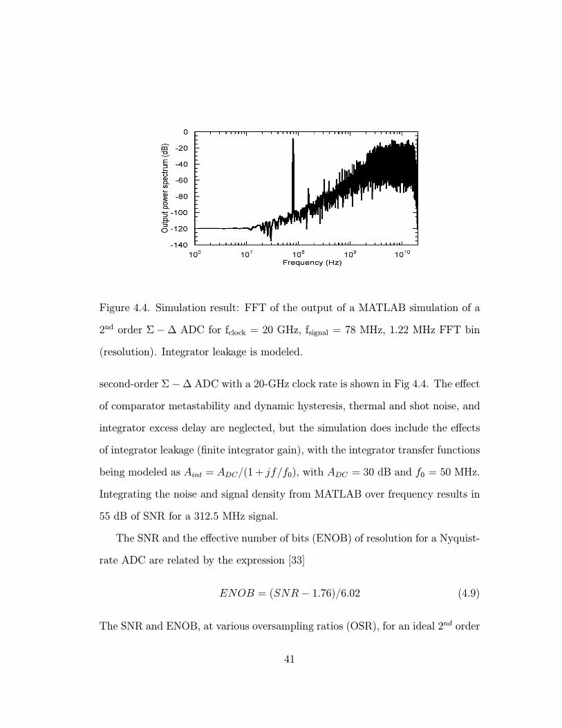
Figure 4.4. Simulation result: FFT of the output of a MATLAB simulation of a
2nd order Σ−∆ ADC for fclock = 20 GHz, fsignal = 78 MHz, 1.22 MHz FFT bin
(resolution). Integrator leakage is modeled.
second-order Σ−∆ ADC with a 20-GHz clock rate is shown in Fig 4.4. The effectof comparator metastability and dynamic hysteresis, thermal and shot noise, and
integrator excess delay are neglected, but the simulation does include the effects
of integrator leakage (finite integrator gain), with the integrator transfer functions
being modeled as Aint = ADC/(1 + jf/f0), with ADC = 30 dB and f0 = 50 MHz.
Integrating the noise and signal density from MATLAB over frequency results in
55 dB of SNR for a 312.5 MHz signal.
The SNR and the effective number of bits (ENOB) of resolution for a Nyquist-
rate ADC are related by the expression [33]
ENOB = (SNR− 1.76)/6.02 (4.9)
The SNR and ENOB, at various oversampling ratios (OSR), for an ideal 2nd order
41
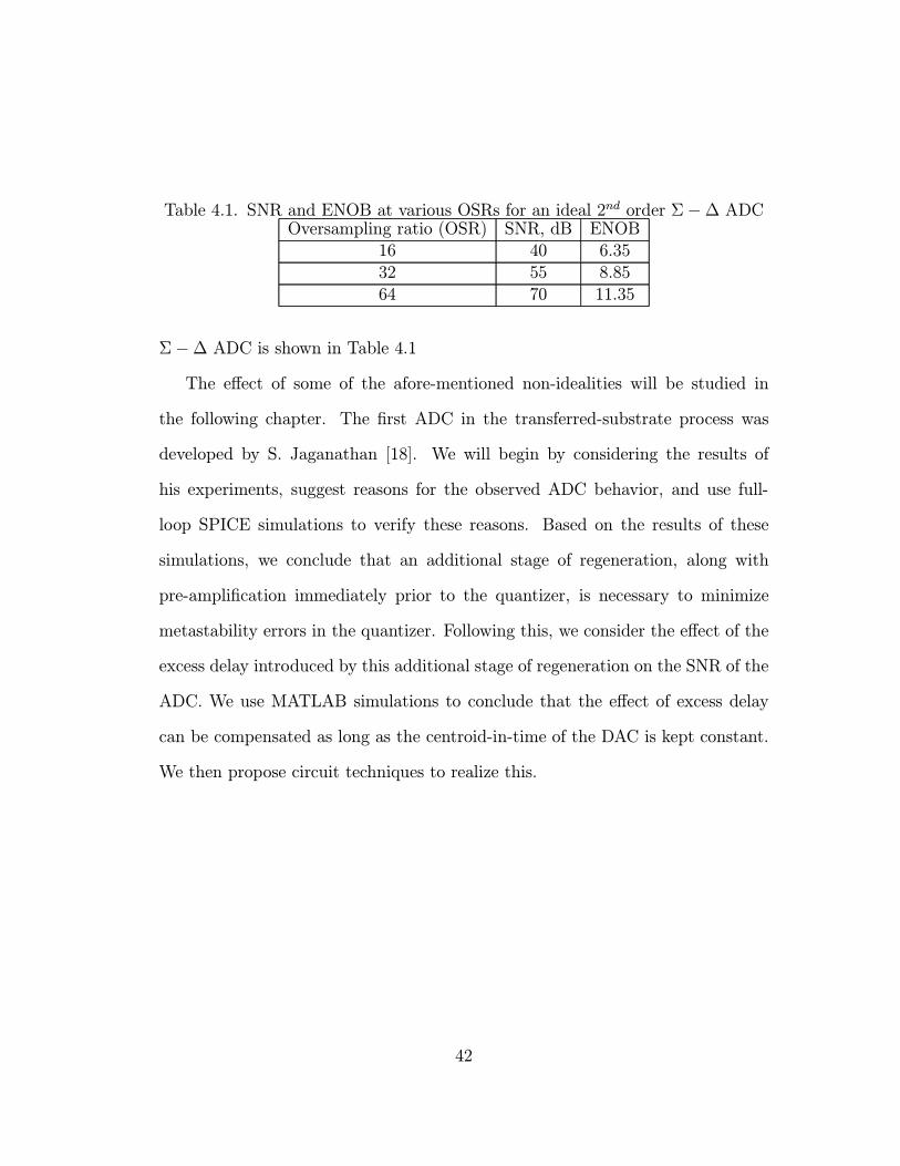
Table 4.1. SNR and ENOB at various OSRs for an ideal 2nd order Σ−∆ ADCOversampling ratio (OSR) SNR, dB ENOB
16 40 6.3532 55 8.8564 70 11.35
Σ−∆ ADC is shown in Table 4.1
The effect of some of the afore-mentioned non-idealities will be studied in
the following chapter. The first ADC in the transferred-substrate process was
developed by S. Jaganathan [18]. We will begin by considering the results of
his experiments, suggest reasons for the observed ADC behavior, and use full-
loop SPICE simulations to verify these reasons. Based on the results of these
simulations, we conclude that an additional stage of regeneration, along with
pre-amplification immediately prior to the quantizer, is necessary to minimize
metastability errors in the quantizer. Following this, we consider the effect of the
excess delay introduced by this additional stage of regeneration on the SNR of the
ADC. We use MATLAB simulations to conclude that the effect of excess delay
can be compensated as long as the centroid-in-time of the DAC is kept constant.
We then propose circuit techniques to realize this.
42

Chapter 5
Design Methodology
The first-generation design, by S. Jaganathan, was a second-order continuous-
time Σ−∆ ADC clocked at 18 GHz [18], and was fabricated in the transferred-
substrate SHBT technology. The circuit used a master-slave latch as the internal
quantizer. To decrease metastability errors in the quantizer, a return-to-zero
(RTZ) DAC was used in the feedback path. Since the output bit-stream could
not be captured digitally at such high data rates, an analog measurement tech-
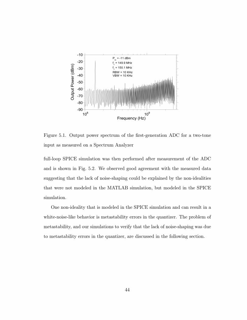
nique was used to quantify ADC-performance. Fig. 5.1 shows the output power
spectrum of the ADC for a two-tone input. No noise-shaping was observed at
frequencies below 1 GHz.
At the time of this design, we did not have sufficiently fast computers in the
lab. For this reason, full-loop SPICE simulation of the design was not possible.
The design of the ADC was hence based on MATLAB simulations. Consequently,
the effect of circuit non-idealities on ADC-performance could not be studied in
detail. Later, after the ICs were fabricated, fast computers were purchased. A
43
-90
-80
-70
-60
-50
-40
-30
-20
-10
108 109
Out
put P
ower
(dBm
)
Frequency (Hz)
Pin
= -11 dBmf1 = 149.9 MHz
f1 = 150.1 MHz
RBW = 10 KHzVBW = 10 KHz
Figure 5.1. Output power spectrum of the first-generation ADC for a two-tone
input as measured on a Spectrum Analyzer
full-loop SPICE simulation was then performed after measurement of the ADC
and is shown in Fig. 5.2. We observed good agreement with the measured data
suggesting that the lack of noise-shaping could be explained by the non-idealities
that were not modeled in the MATLAB simulation, but modeled in the SPICE
simulation.
One non-ideality that is modeled in the SPICE simulation and can result in a
white-noise-like behavior is metastability errors in the quantizer. The problem of
metastability, and our simulations to verify that the lack of noise-shaping was due
to metastability errors in the quantizer, are discussed in the following section.
44

-110
-100
-90
-80
-70
-60
-50
-40
-30
1 10 100 1000 10000
Out
put S
pect
rum
(arb
. log
. uni
ts)
Frequency (MHz)
SPICE SIMULATIONfsignal
= 78.125 MHz
fclock
= 20 GHz
Figure 5.2. Simulation result: FFT of the output of a SPICE simulation of the
first-generation design for fclock = 20 GHz, fsignal = 78.125 MHz, 2.44 MHz FFT
bin (resolution)
5.1 Metastability
Metastability errors arise as a result of the internal-quantizer’s inability to
regenerate to a logic level before the quantizer latch is disabled. With an ideal
1-bit quantizer, the output (of the quantizer) depends only on whether its input
is positive or negative. Hence, inputs of varying signal strength will result in
the same output as long as they are either all positive or all negative. Since the
output of the quantizer drives a 1-bit DAC, the amount of charge fed back to
the integrator is independent of the quantizer-input’s strength. In a non-ideal
situation, as a result of transistor parasitics and interconnect delays, the output
rise-time will depend on the input signal strength. For this reason, the duration
of the output pulse will depend on the quantizer-input (Fig. 5.3). Consequently,
45
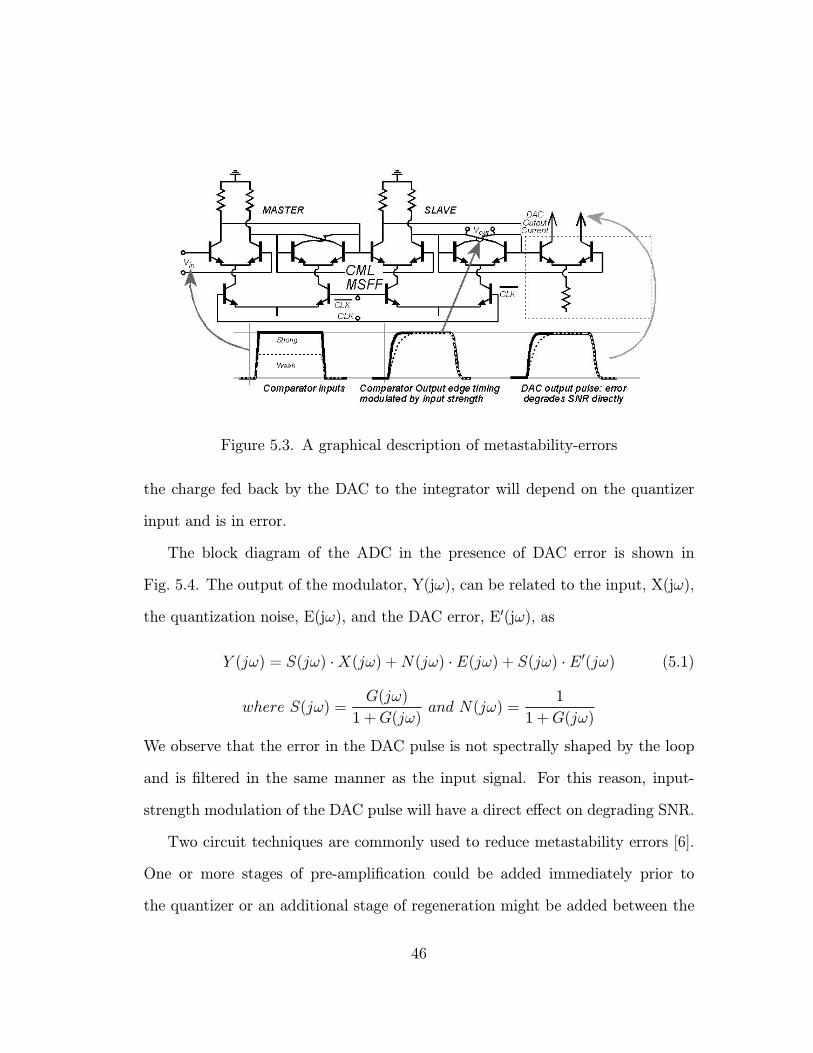
Figure 5.3. A graphical description of metastability-errors
the charge fed back by the DAC to the integrator will depend on the quantizer
input and is in error.
The block diagram of the ADC in the presence of DAC error is shown in
Fig. 5.4. The output of the modulator, Y(jω), can be related to the input, X(jω),
the quantization noise, E(jω), and the DAC error, E0(jω), as
Y (jω) = S(jω) ·X(jω) +N(jω) · E(jω) + S(jω) · E0(jω) (5.1)
where S(jω) =G(jω)
1 +G(jω)and N(jω) =
1
1 +G(jω)
We observe that the error in the DAC pulse is not spectrally shaped by the loop
and is filtered in the same manner as the input signal. For this reason, input-
strength modulation of the DAC pulse will have a direct effect on degrading SNR.
Two circuit techniques are commonly used to reduce metastability errors [6].
One or more stages of pre-amplification could be added immediately prior to
the quantizer or an additional stage of regeneration might be added between the
46

8. / 9. / 92. / :. /
;. /
1 11
<. /
*
1
1
;2. /
Figure 5.4. Linear model of the ADC in the presence of DAC error
! 1
*5 @*,*,
45#
Figure 5.5. Circuit block-diagram for metastability analysis
quantizer and the DAC [20]. While the former results in an increased quantizer
input, the latter technique allows the quantizer more time to attain a full logic
level. We investigate the effect of both the techniques on noise-shaping by using
full-loop SPICE simulations. The circuit block-diagram for the simulations is
shown in Fig. 5.5. Since an additional stage of regeneration has been added, the
quantizer is now a master-slave-slave latch. We performed two simulations, one
with the pre-amplifier and one without.
47

Figure 5.6. Analyzing full-loop SPICE-simulation data
The SPICE simulations are performed over a number of clock cycles (10,000)
to allow the Σ − ∆ loop to settle and the results of the transient simulations
are analyzed as follows. The output data from the transient simulation is read
into a MATLAB program, where the data is first hard-limited to simulate a logic
analyzer. A 8192-point fast-Fourier transform (FFT) is then performed to obtain
the output-power-spectrum (Fig. 5.6). In the following simulations, a two-stage
Cherry-Hooper based pre-amplifier is used immediately prior to the quantizer.
The pre-amplifier has a DC gain of 17.5 dB and a −3 dB bandwidth of 50 GHz.Such a pre-amplifier was sufficient for our needs, and hence, no attempt was made
in circuit design to further improve its performance. In all these simulations, the
ADC is clocked at 20 GHz.
Fig. 5.7 illustrates the effect of both pre-amplification and additional regen-
eration on metastability-errors in the quantizer. We observe that both circuit-
techniques have a profound impact in shaping the quantization-noise. By using
just an additional stage of regeneration, noise-shaping is observed to frequencies
48

< 200 MHz (an oversampling ratio > 32). With pre-amplification, the noise-floor
reduces by an additional 10 dB at low frequencies (∼ 100 MHz). From the dif-
ference in noise-shaping in the two instances, we can also conclude that, at this
clock-frequency, an additional stage of regeneration, in itself, is not sufficient to
eliminate metastability errors in the quantizer. For this reason, our initial design
uses an additional stage of regeneration along with pre-amplification. For the re-
mainder of this thesis, we will refer to our initial design as the second-generation
ADC. We attempted to fabricate the second-generation ADC in the transferred-
substrate DHBT process but owing to a number of process problems (discussed
in Chapter 3), we were never able to realize the design.
Concurrent with the fabrication attempts, we also tried to study the effect of
the excess delay introduced by the additional stage of regeneration on the SNR
of the ADC. Towards this end, we compared the output power spectrum of the
second-generation ADC relative to two MATLAB-based idealized-ADC simula-
tions, one with a MSS-latch-based quantizer and the other with a MS-latch based
quantizer (Fig. 5.8). At signal frequencies larger than 100 MHz, no difference
in SNR is observed between the second-generation design and the idealized-ADC
with the same circuit topology. The additional stage of regeneration, though, de-
grades SNR relative to a MS-latch-based quantizer. Thus, while SNR is improved
through suppression of metastability errors by additional latching, the excess de-
lay associated with the additional regeneration stages degrades the SNR. This is
a major design issue. We will now consider it in detail.
49

-120
-100
-80
-60
-40
-20
0
106 107 108 109 1010
Out
put P
ower
Spe
ctru
m (d
BFS
)
Frequency (Hz)
without pre-amplifier
with pre-amplifier
Figure 5.7. Simulation result: FFT of the output of two 2nd order Σ−∆ ADCs forfclock = 20 GHz, fsignal = 78 MHz, 2.44 MHz FFT bin (resolution). Both circuits
use a master-slave-slave latch as the comparator; one of them uses a pre-amplifier
immediately prior to the quantizer
50

-120
-110
-100
-90
-80
-70
-60
-50
106 107 108 109 1010
Out
put P
ower
Spe
ctru
m (d
BFS
)
Frequency (Hz)
SPICE
Ideal M-S latchIdeal M-S-S latch
Figure 5.8. Simulation result: FFT of the output of 3 different ADC output bit-
streams. a) a MATLAB simulation of a 2nd order Σ−∆ ADC for fclock = 20 GHzwith a master-slave latch based quantizer, b) a MATLAB simulation of a 2nd order
Σ−∆ ADC for fclock = 20 GHz with a master-slave-slave latch based quantizer,
c) a SPICE simulation of the second generation ADC for fclock = 20 GHz, fsignal
= 78 MHz, 2.44 MHz FFT bin (resolution)
51

5.2 Excess Delay
The effect of excess delay on ADC-resolution is well known [4, 13, 14] and
has been studied in detail [7]. In [7], Cherry et al study the effect of excess
delay by considering the equivalence between continuous-time and discrete-time
Σ−∆ ADCs. Using such an approach, they are able to predict SNR-degradationin the presence of excess delay and propose solutions to compensate the loss in
performance. Here, we provide an alternate analysis of SNR degradation in the
presence of excess delay. We begin by computing the noise transfer function,
N(jω), in the presence of excess delay in the loop.
The most common design procedure for continuous-time Σ−∆modulators is tostart with a discrete-time transfer function that will provide maximum baseband
attenuation of quantization noise. The discrete-time transfer function is then
transformed to the continuous-time domain to obtain a continuous-time transfer
function. The noise transfer function, N(z), for a 2nd order modulator is given by
N(z) = (1− z−1)2 (5.2)
This leads to a choice of loop filter transfer function to be
G(z) =2z − 1(z − 1)2 (5.3)
The equivalent continuous-time transfer function for the discrete-time filter is
given by [7]
G(s) =1 + 1.5sTss2T 2s
(5.4)
where Ts = 1/fs represents the sampling time. Any excess delay, τ , can be repre-
sented as e−jωτ in the frequency domain and is simply a multiplying factor in the
52
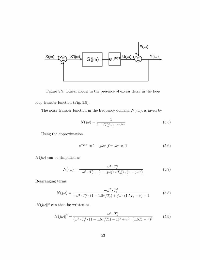
8. /9. / 92. /1 <. /
*
:. /
;. /
11
*
Figure 5.9. Linear model in the presence of excess delay in the loop
loop transfer function (Fig. 5.9).
The noise transfer function in the frequency domain, N(jω), is given by
N(jω) =1
1 +G(jω) · e−jωτ (5.5)
Using the approximation
e−jωτ ≈ 1− jωτ for ωτ ¿ 1 (5.6)
N(jω) can be simplified as
N(jω) =−ω2 · T 2s
−ω2 · T 2s + (1 + jω(1.5Ts)) · (1− jωτ )(5.7)
Rearranging terms
N(jω) =−ω2 · T 2s
−ω2 · T 2s · (1− 1.5τ/Ts) + jω · (1.5Ts − τ ) + 1(5.8)
|N(jω)|2 can then be written as
|N(jω)|2 = ω4 · T 4s(ω2 · T 2s · (1− 1.5τ/Ts)− 1)2 + ω2 · (1.5Ts − τ )2
(5.9)
53

Instead of attempting to solve this equation rigorously, we will consider the effect
of τ on |N(jω)|2 at low frequencies. In other words, we will study the effect ofexcess delay on the in-band noise suppression. At low frequencies, the denominator
of |N(jω)|2 simplifies to its constant term, in this case, unity. |N(jω)|2 hencesimplifies as
|N(jω)|2 = ω4 · T 4s (5.10)
an expression that is independent of the excess delay, τ . It must be noted here
that we would have arrived at the same result even if we had not used the ap-
proximation of Eq. 5.6. Hence, a linearized-model based analysis predicts that
excess delay has no effect on the in-band suppression of the quantization noise at
low frequencies, and consequently, on the resolution of the ADC at high OSRs.
To verify our analysis, we use MATLAB to compute the transfer function in the
two cases, i.e. with no excess delay in the loop and with an excess delay of 25 ps
in the loop. The two functions show very good agreement for frequencies below 2
GHz (Fig. 5.10). We also observe that in the presence of excess delay, the change
in damping factor manifests itself in the form of considerable resonance-peaking
at frequencies around 5 GHz.
Further, using the approximation of Eq. 5.6, it can be shown that by introduc-
ing a zero with a time constant τ in the loop, one can compensate for the excess
delay over a wider range of frequencies. Fig. 5.11 compares the transfer function
in the two cases, viz., no excess delay and an excess-delay of 25 ps present, but
compensated by altering the zero-location. We observe excellent agreement be-
tween the two cases for frequencies below 3 GHz. At higher frequencies, ωτ is no
54
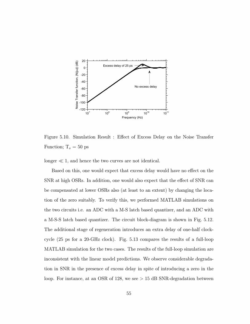
-120
-100
-80
-60
-40
-20
0
20
107 108 109 1010 1011
Noi
se T
rans
fer f
unct
ion,
|N(jω
)| (d
B)
Frequency (Hz)
Excess delay of 25 ps
No excess delay
Figure 5.10. Simulation Result : Effect of Excess Delay on the Noise Transfer
Function; Ts = 50 ps
longer ¿ 1, and hence the two curves are not identical.
Based on this, one would expect that excess delay would have no effect on the
SNR at high OSRs. In addition, one would also expect that the effect of SNR can
be compensated at lower OSRs also (at least to an extent) by changing the loca-
tion of the zero suitably. To verify this, we performed MATLAB simulations on
the two circuits i.e. an ADC with a M-S latch based quantizer, and an ADC with
a M-S-S latch based quantizer. The circuit block-diagram is shown in Fig. 5.12.
The additional stage of regeneration introduces an extra delay of one-half clock-
cycle (25 ps for a 20-GHz clock). Fig. 5.13 compares the results of a full-loop
MATLAB simulation for the two cases. The results of the full-loop simulation are
inconsistent with the linear model predictions. We observe considerable degrada-
tion in SNR in the presence of excess delay in spite of introducing a zero in the
loop. For instance, at an OSR of 128, we see > 15 dB SNR-degradation between
55

-120
-100
-80
-60
-40
-20
0
20
107 108 109 1010 1011
Noi
se T
rans
fer f
unct
ion,
|N(jω
)| (d
B)
Frequency (Hz)
No excess delay
Excess delay of 25 ps
Excess delay of 25 pscompensated by
altering zero-location
Figure 5.11. Simulation Result : Altering the Zero-location to compensate for the
effect of excess delay on the Noise Transfer Function; Ts=50 ps
the two cases.
Given the inconsistency between the linear model’s prediction and the MAT-
LAB simulation, and the fact that the additive white-noise approximation does
not hold for a 1-bit quantizer, we conclude that the linear model cannot be used to
explain the dynamics of an ADC with a 1-bit internal quantizer. To substantiate
this point, we also compare the output power spectra of the two circuit topolo-
gies when a multi-bit internal quantizer is employed (Fig. 5.14). We observe that
the two spectra show much better agreement in this case. This is not surprising,
considering that the linearity of the system, and hence the validity of the linear
model, increases with the resolution of the internal quantizer.
Since the quantizer’s output depends on its input at the sampling instants, it
should be possible to recover the loss in SNR by restoring the quantizer inputs
to their original values (i.e., the case where the additional stage of regeneration is
56
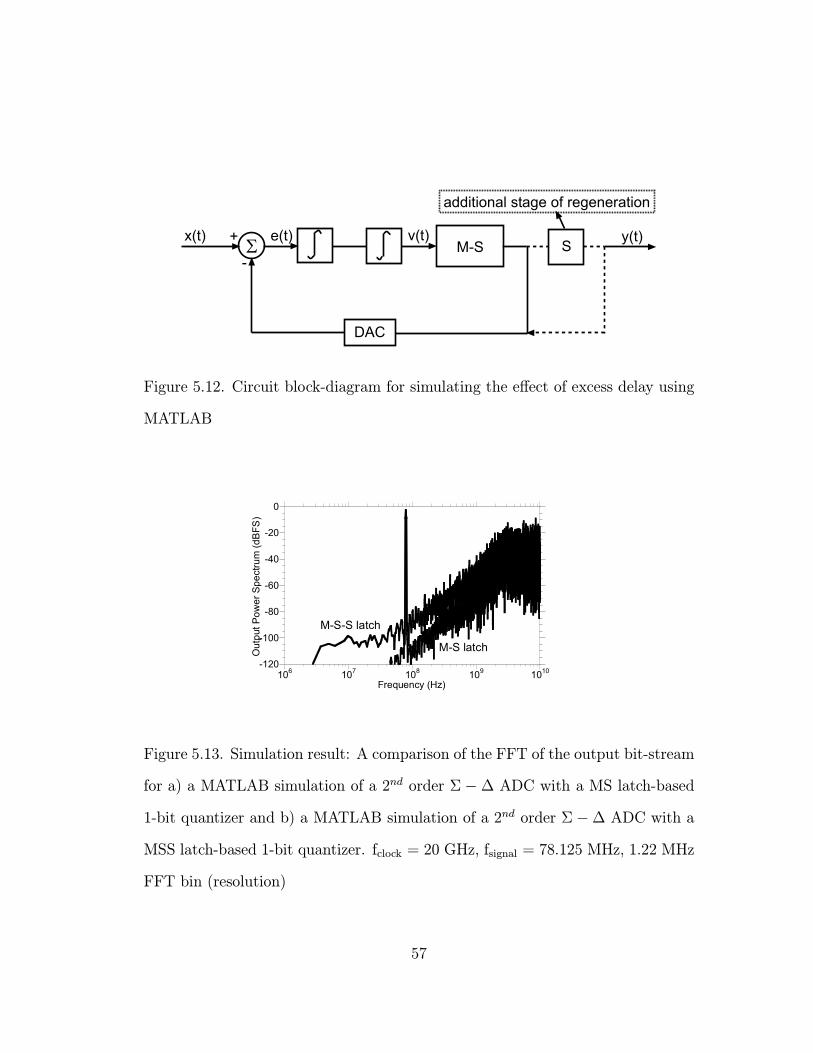
0./ 1
*@*,
45#
-././,
"!""'!"!
./
Figure 5.12. Circuit block-diagram for simulating the effect of excess delay using
MATLAB
-120
-100
-80
-60
-40
-20
0
106 107 108 109 1010
Out
put P
ower
Spe
ctru
m (d
BFS
)
Frequency (Hz)
M-S-S latch
M-S latch
Figure 5.13. Simulation result: A comparison of the FFT of the output bit-stream
for a) a MATLAB simulation of a 2nd order Σ −∆ ADC with a MS latch-based
1-bit quantizer and b) a MATLAB simulation of a 2nd order Σ −∆ ADC with a
MSS latch-based 1-bit quantizer. fclock = 20 GHz, fsignal = 78.125 MHz, 1.22 MHz
FFT bin (resolution)
57
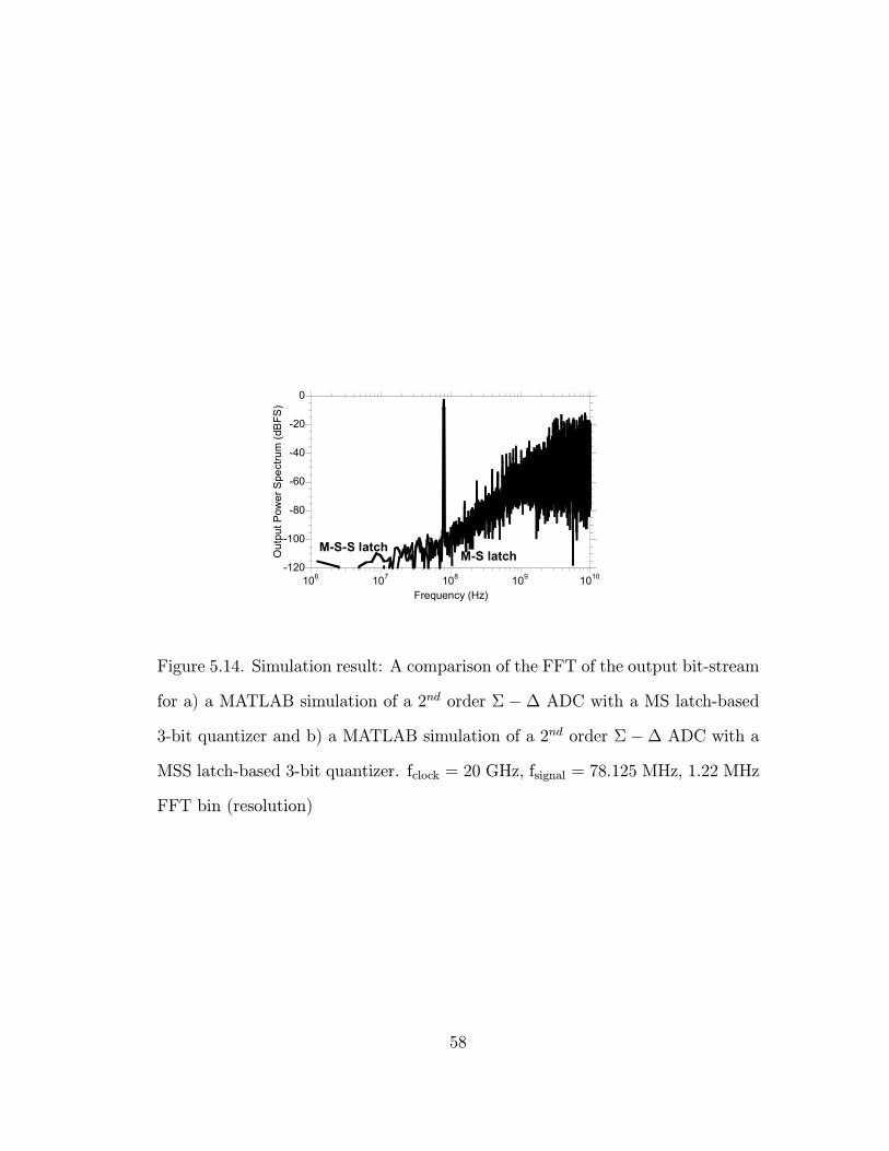
-120
-100
-80
-60
-40
-20
0
106 107 108 109 1010
Out
put P
ower
Spe
ctru
m (d
BFS)
Frequency (Hz)
M-S latchM-S-S latch
Figure 5.14. Simulation result: A comparison of the FFT of the output bit-stream
for a) a MATLAB simulation of a 2nd order Σ −∆ ADC with a MS latch-based
3-bit quantizer and b) a MATLAB simulation of a 2nd order Σ −∆ ADC with a
MSS latch-based 3-bit quantizer. fclock = 20 GHz, fsignal = 78.125 MHz, 1.22 MHz
FFT bin (resolution)
58

absent) at the clock transitions. Further, since the quantizer inputs depend on the
timing and the duration of the DAC pulse, it should be possible to compensate
for the loss in SNR by monitoring the centroid-in-time of the DAC pulse, and
ensuring that it remains stationary.
Consider the timing diagram shown in Fig. 5.15. We will use the falling-edge of
the clock as our reference point and compare the centroids-in-time for the different
cases relative to it. With a M-S latch based quantizer (Fig. 5.15a) and a NRZ
DAC, the centroid-in-time is Tclk/2 away from the clock transition. With a M-S-S
latch based quantizer (Fig. 5.15b) and a NRZ DAC, the centroid is Tclk from the
clock transition. If our arguments hold, we should be able to recover any loss in
SNR between cases (a) and (b) using the DAC pulse shown in Fig. 5.15c. Such a
DAC pulse, though, cannot be realized with a M-S-S latch based quantizer. With
a M-S-S latch based quantizer, the DAC pulse will have to be a delta function (at
∆T = Tclk/2) to maintain the position of its centroid-in-time constant. In order
to obtain a reasonable compromise between excess delay and circuit realizability,
we use a RTZ-DAC (Fig. 5.15d) whose centroid-in-time is 3Tclk/4 away from the
clock transition. We find that the excess delay of Tclk/4 (relative to case (a))
can be neutralized by changing the location of the zero in the transfer function.
Excellent agreement is observed between the output power spectra in the two
cases (Fig. 5.16).
Based on these observations, we have designed two ADCs in the mesa-HBT
technology. Both designs use a M-S-S latch as the internal quantizer. While one
design uses a NRZ DAC, the other uses a RTZ DAC to compensate for the excess
59
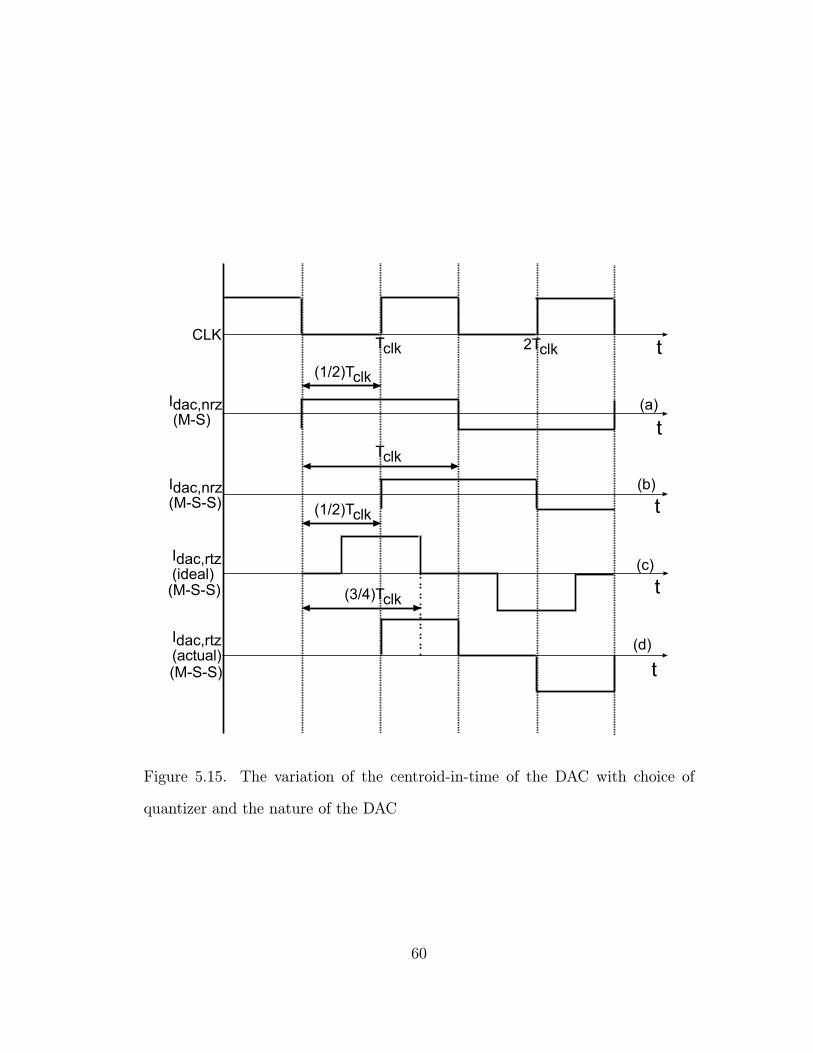
A A
.B/A
.B/A
A
#+C
D"!7.@*,/
D"!7.@*,*,/
.B/A
."/
.3/
./
./D"7.""/.@*,*,/
D"7."/
.@*,*,/
Figure 5.15. The variation of the centroid-in-time of the DAC with choice of
quantizer and the nature of the DAC
60

-120
-100
-80
-60
-40
-20
0
106 107 108 109 1010
Out
put P
ower
Spe
ctru
m (d
BFS)
Frequency (Hz)
MSS latch; RTZ DACττττ
z changed
MS latch
Figure 5.16. Simulation result: A comparison of the FFT of the output bit-stream
of a) a MATLAB simulation of a 2nd order Σ − ∆ ADC with a MS latch and a
NRZ DAC. b) a MATLAB simulation of a 2nd order Σ − ∆ ADC with a MSS
latch and a RTZ DAC with the zero-location altered suitably. In both cases, fclock
= 20 GHz, fsignal = 78.125 MHz, 1.22 MHz FFT bin (resolution)
61

delay introduced by the additional stage of regeneration. We discuss the design of
the various circuit blocks in the following section. To minimize circuit complexity,
we do not use a pre-amplifier immediately prior to the quantizer. Considering
this, and based on our studies on metastability errors in the quantizer, these
circuits are designed for a 10-GHz clock rate. In addition, since commercial 1:16
10G demultiplexers are available, the output bit-stream can be demultiplexed and
digitally acquired using a Logic Analyzer.
5.3 Circuit Design
A single-ended block diagram of the ADC is shown in Fig. 5.17. Our actual
designs adopt a fully differential architecture. The advantages of such an architec-
ture include significant suppression of even-harmonic distortion, a 6-dB increase
in dynamic range and reduction in extraneous signals such as power supply noise
and clock switching noise. The design of the integrators, the DACs and the com-
parator are discussed in detail below. The clock signal to the circuit is available
in a single-ended form from the synthesizer. Clock buffers are used on wafer to
convert the signal to differential form. This differential clock signal feeds the
comparator and the RTZ DAC.
5.3.1 Integrator-1
The circuit schematic for the first integrator in the loop is shown in Fig. 5.18.
Transistors Q3, Q4, Q7 and Q8, in association with the degeneration resistance,
62
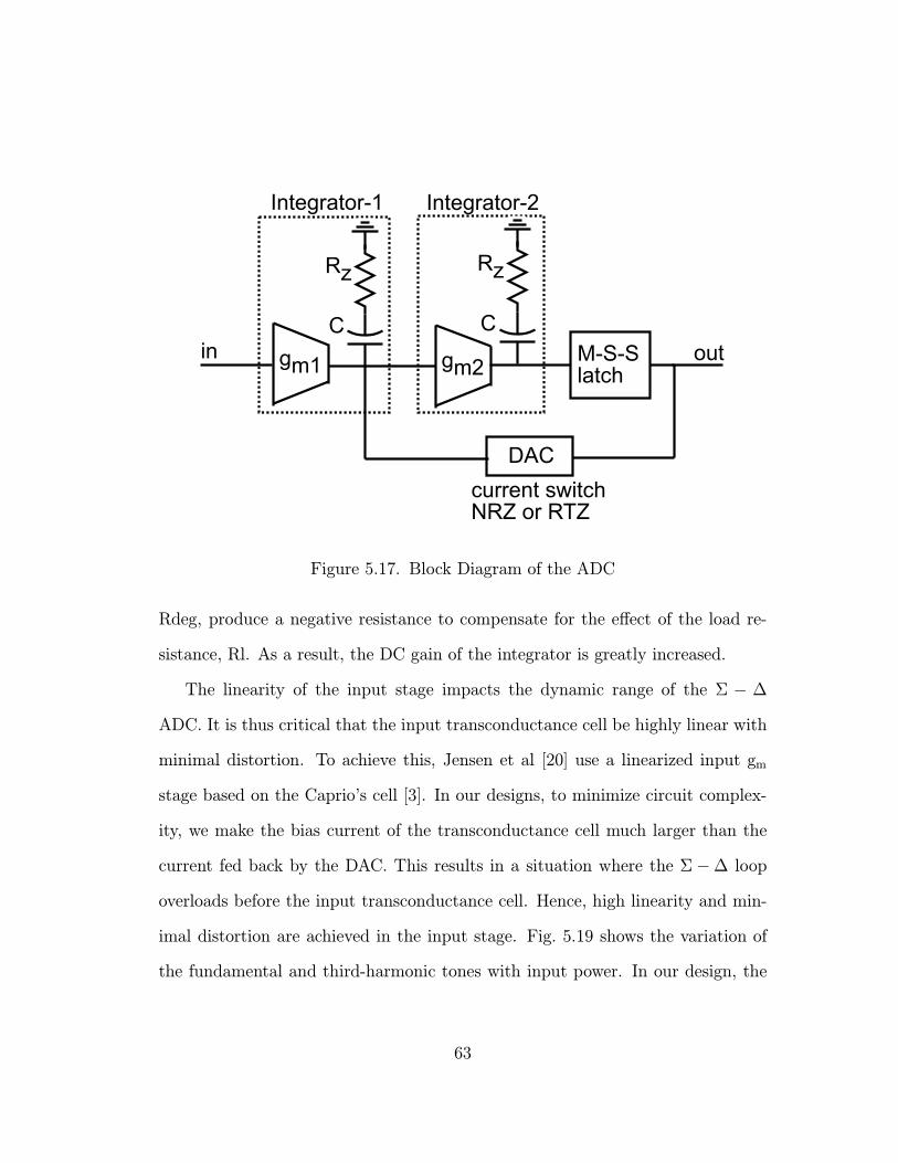
45#
D!"* D!"*
@*,*,")
!
!E)F&G&AG
#
&7 &7
#
Figure 5.17. Block Diagram of the ADC
Rdeg, produce a negative resistance to compensate for the effect of the load re-
sistance, Rl. As a result, the DC gain of the integrator is greatly increased.
The linearity of the input stage impacts the dynamic range of the Σ − ∆ADC. It is thus critical that the input transconductance cell be highly linear with
minimal distortion. To achieve this, Jensen et al [20] use a linearized input gm
stage based on the Caprio’s cell [3]. In our designs, to minimize circuit complex-
ity, we make the bias current of the transconductance cell much larger than the
current fed back by the DAC. This results in a situation where the Σ−∆ loop
overloads before the input transconductance cell. Hence, high linearity and min-
imal distortion are achieved in the input stage. Fig. 5.19 shows the variation of
the fundamental and third-harmonic tones with input power. In our design, the
63
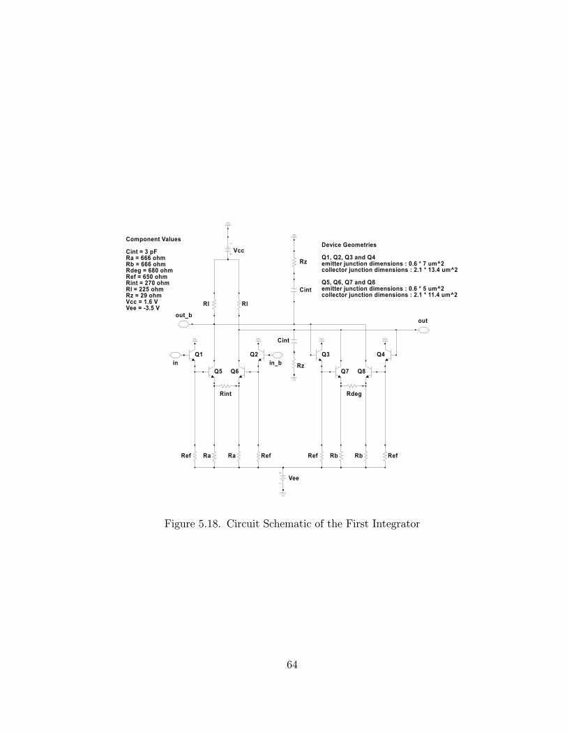
!"
## !$ ""%&'( )!$ ""%'(' )
## !$ ""%&'( )!$ ""%'(' )
*"
+*,+- +- +&- +&- +&- +- +.- +'+/'
Figure 5.18. Circuit Schematic of the First Integrator
64

-160
-120
-80
-40
0
-35 -30 -25 -20 -15 -10 -5
Out
put (
dBm
)
Input (dBm)
-7.5 dBm
intermodulation suppressionof 88 dBc
Third Harmonic
Fundamental
Figure 5.19. Simulation result: SPICE simulation of the linearity of the integrator.
We observe an intermodulation suppression of 88 dBc at an input power of -7.5
dBm
ADC overloads at an input power, Pin,max, of -7.5 dBm. At this input power, we
observe an intermodulation suppression of 88 dBc.
In addition, the input stage contributes thermal and shot noise, and can limit
the SNR. Referring to the partial circuit schematic of Fig. 5.20, the ADC total
input-referred noise voltage arising from thermal and shot noise has a spectral
density given by
dhE2nidf
' 4kT (kT/qIc)
+ 8kT (Rdeg +Rex +Rbb + Z0/2)
+ 4qIb(Rdeg + Rex +Rbb + Z0/2)2
+ (8kT/Rcs)γ2(Rdeg +Rex + kT/qIc)
2
+ 4kT
ÃkT
qIDAC/2
!(Rdeg +Rex + kT/qIc)
2
R2cs,DAC
65

Figure 5.20. Detail of input gm stage and RTZ DAC for noise analysis.
+ 8kT(Rdeg +Rex + kT/qIc)
2
Rcs,DAC,
where Ic is the input stage bias current, Ib its base current, Rbb the input-stage
base resistance, Z0 = 50 Ω the input interface impedance, IDAC the DAC switched
current, and γ the fractional imbalance in DC bias currents in the input differential
pair. The input noise to the maximum input voltage before ADC overload is given
by, Vin,max = IDAC(Rdeg + Rex + kT/qIc). Given the IC design values, the input-
noise limited SNR is 153 dB (1 Hz).
5.3.2 Integrator-2
The circuit schematic for the second integrator in the loop is shown in Fig. 5.18.
Transistors Q3, Q4, Q7 and Q8, in association with the degeneration resistance,
Rdeg, produce a negative resistance that compensates for the effect of the load
66

#$!!%"
#!($?&"()&3()&()&'( )&!()&()&7()%( %%(*%
48
"! !!!! H !!!!H
I3
!I3! &7
%
%
&7
#!
#!
&
&'&3&3&' &'&"&"&'
&!
&&
Figure 5.21. Circuit Schematic of the Second Integrator
resistance, Rl. This results in a much higher DC gain for the integrator. The gain
and phase characteristics of the gm-stage are shown in Fig. 5.22. The DC gain is
31 dB and the low frequency pole is at 30 MHz.
Due to parasitics inherent in the device as well as the layout, the circuit
implementation of the gm-stage has a second pole. This second pole contributes
excess phase at frequencies much smaller than the location of the second pole. The
excess phase results in excess delay and hence, it is imperative that the second
pole be located at a frequency much higher than the clock rate. In our design,
the second pole is located at 55 GHz, contributes an excess delay of ∼ 3 ps, and
67
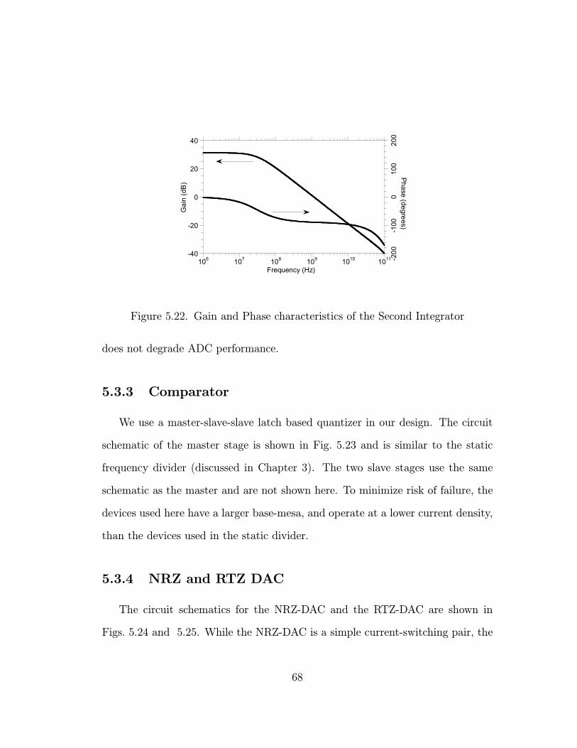
-40
-20
0
20
40
-200
-100
010
020
0
106 107 108 109 1010 1011
Gai
n (d
B)Phase (degrees)
Frequency (Hz)
Figure 5.22. Gain and Phase characteristics of the Second Integrator
does not degrade ADC performance.
5.3.3 Comparator
We use a master-slave-slave latch based quantizer in our design. The circuit
schematic of the master stage is shown in Fig. 5.23 and is similar to the static
frequency divider (discussed in Chapter 3). The two slave stages use the same
schematic as the master and are not shown here. To minimize risk of failure, the
devices used here have a larger base-mesa, and operate at a lower current density,
than the devices used in the static divider.
5.3.4 NRZ and RTZ DAC
The circuit schematics for the NRZ-DAC and the RTZ-DAC are shown in
Figs. 5.24 and 5.25. While the NRZ-DAC is a simple current-switching pair, the
68

*"
0+- "+&- +- +- +/'
!"
####.#&## !$ ""%&'(. )!$ ""%'(' )
#### !$ ""%&'( )!$ ""%'(' )
0 0
"0 0
&
.
Figure 5.23. Circuit Schematic of the Master Stage of the Comparator
69

*"
+&- +&- +/'
!"
!$ ""%&'( )!$ ""%'(' )
!$ ""%&'( )!$ ""%'(' )
Figure 5.24. Circuit Schematic of the NRZ DAC
RTZ-DAC has two levels of switching, one for the data and one for the clock. To
maintain the charge fed back by the DAC constant in the two cases, the RTZ
DAC uses a bias current 4 times higher than the NRZ DAC.
We perform SPICE simulations on the two designs to verify full-loop behavior.
The output power spectra for the NRZ-DAC-based ADC and RTZ-DAC-based
ADC are shown in Figs. 5.26 and 5.27, respectively.
The following chapter discusses the measured results of these ADCs.
70
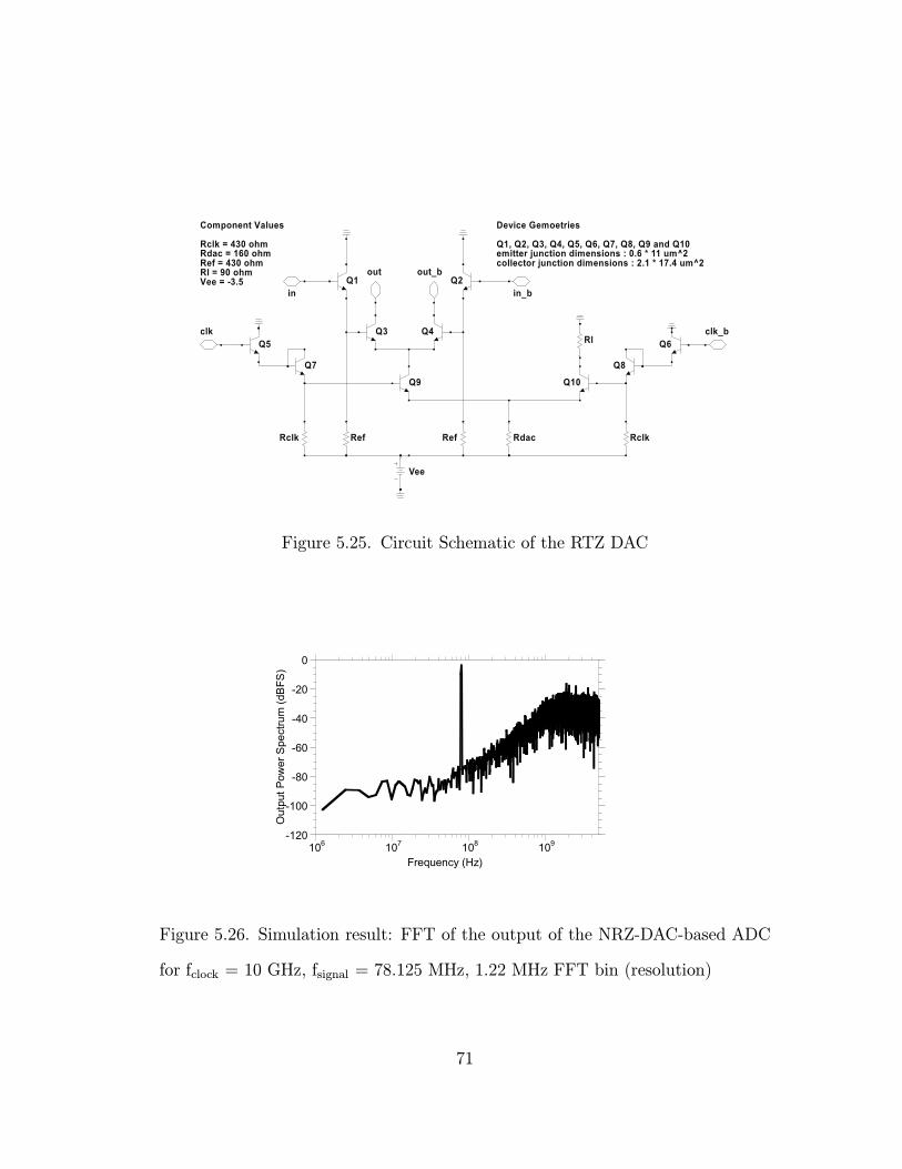
*"
0+&- +&- +&- +.&- +/'
!"
########.& !$ ""%&'( )!$ ""%'(' )
00
0 0
&.
Figure 5.25. Circuit Schematic of the RTZ DAC
-120
-100
-80
-60
-40
-20
0
106 107 108 109
Out
put P
ower
Spe
ctru
m (d
BFS)
Frequency (Hz)
Figure 5.26. Simulation result: FFT of the output of the NRZ-DAC-based ADC
for fclock = 10 GHz, fsignal = 78.125 MHz, 1.22 MHz FFT bin (resolution)
71
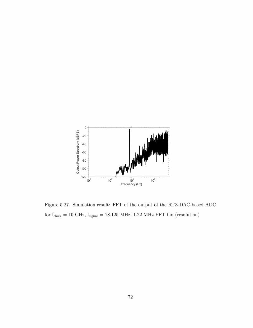
-120
-100
-80
-60
-40
-20
0
106 107 108 109
Out
put P
ower
Spe
ctru
m (d
BFS)
Frequency (Hz)
Figure 5.27. Simulation result: FFT of the output of the RTZ-DAC-based ADC
for fclock = 10 GHz, fsignal = 78.125 MHz, 1.22 MHz FFT bin (resolution)
72

Chapter 6
ADC Results
In this chapter, our methods to quantify ADC-performance are first explained.
A comparison of the output-power-spectrums of the NRZ-DAC-based ADC and
RTZ-DAC-based ADCs is then presented. Following this, results from a digital-
acquisition-based measurement are presented. We show both one-tone and two-
tone measurements and draw conclusions on ADC-resolution and third-order dis-
tortion.
6.1 Σ−∆ ADC: Test Set-Up
For testing purposes, we directly capture the single-bit data stream of the
Σ−∆ modulator and perform an FFT on the captured output to determine the
performance of the ADC. Viewing the single-bit output on an analog spectrum
analyzer performs the Fourier transform in real time and gives a qualitative indi-
cation of the ADC performance. However, the noise floor of the analog spectrum
73

Figure 6.1. ADC Measurement Set-up for Digital Capture
analyzer limits us to a dynamic range of 80 dB and hence, does not let us view
the noise-shaping at low frequencies. It is thus necessary to capture the digital
data stream at the high data rates and perform the FFT. The test set-up for such
a measurement is shown in Fig. 6.1.
The output bit-stream at 8 Gbps is first demultiplexed into 16 channels of
500 Msps each. The data from the 16 channels are then captured using a logic
analyzer and transferred to a computer. The original 8 Gbps bit-stream is then
reconstructed in software and a MATLAB-based program is used to perform the
FFT on this reconstructed bit-stream. To minimize spectral leakage due to time
truncation, it is important to set the input sine-wave frequency to be an integral
multiple of fclk divided by the FFT length. We perform a 131072-point FFT for
both one-tone and two-tone measurements.
74
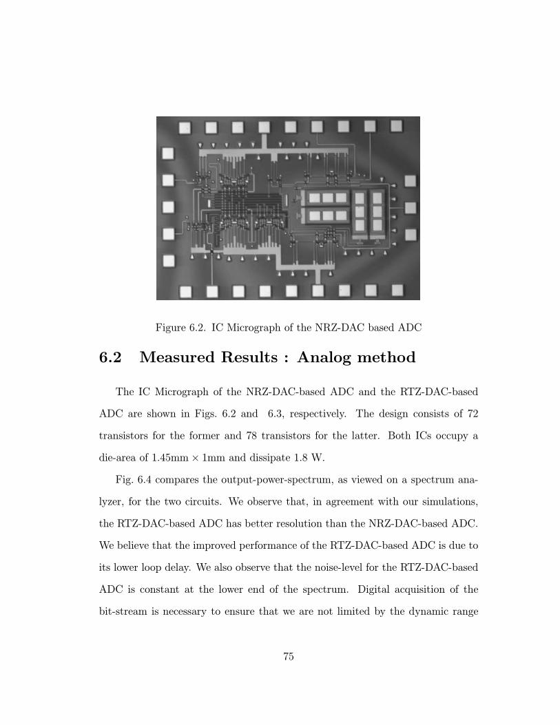
Figure 6.2. IC Micrograph of the NRZ-DAC based ADC
6.2 Measured Results : Analog method
The IC Micrograph of the NRZ-DAC-based ADC and the RTZ-DAC-based
ADC are shown in Figs. 6.2 and 6.3, respectively. The design consists of 72
transistors for the former and 78 transistors for the latter. Both ICs occupy a
die-area of 1.45mm× 1mm and dissipate 1.8 W.
Fig. 6.4 compares the output-power-spectrum, as viewed on a spectrum ana-
lyzer, for the two circuits. We observe that, in agreement with our simulations,
the RTZ-DAC-based ADC has better resolution than the NRZ-DAC-based ADC.
We believe that the improved performance of the RTZ-DAC-based ADC is due to
its lower loop delay. We also observe that the noise-level for the RTZ-DAC-based
ADC is constant at the lower end of the spectrum. Digital acquisition of the
bit-stream is necessary to ensure that we are not limited by the dynamic range
75
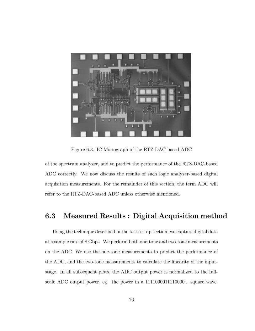
Figure 6.3. IC Micrograph of the RTZ-DAC based ADC
of the spectrum analyzer, and to predict the performance of the RTZ-DAC-based
ADC correctly. We now discuss the results of such logic analyzer-based digital
acquisition measurements. For the remainder of this section, the term ADC will
refer to the RTZ-DAC-based ADC unless otherwise mentioned.
6.3 Measured Results : Digital Acquisition method
Using the technique described in the test set-up section, we capture digital data
at a sample rate of 8 Gbps. We perform both one-tone and two-tone measurements
on the ADC. We use the one-tone measurements to predict the performance of
the ADC, and the two-tone measurements to calculate the linearity of the input-
stage. In all subsequent plots, the ADC output power is normalized to the full-
scale ADC output power, eg. the power in a 1111000011110000.. square wave.
76

-80
-70
-60
-50
-40
-30
-20
-10
0
0 5 108 1 109 1.5 109
Out
put P
ower
Spe
ctru
m (d
B)
Frequency (Hz)
RBW = 3 MHzVBW = 10 KHz
NRZ DAC
RTZ DAC
Figure 6.4. A Comparison of the Output Power Spectra of the NRZ-DAC-based
ADC and the RTZ-DAC-based ADC as measured on an analog spectrum analyzer
An unsaturated sinusoidal output can have at most -3 dB output power relative
to the full-scale signal.
6.3.1 One-tone Measurements
Fig. 6.5 plots the calculated 131072-point FFT spectrum for a 62.5-MHz input.
The oversampling ratio (OSR) is 64 and the input power is 3 dBm. For single-tone
measurements, the SNR and the effective number of bits (ENOB) of resolution
for a Nyquist-rate ADC are related by the expression
ENOB = (SNR− 1.76)/6.02
[33]. We have calculated the SNR and ENOB using the noise power measured
at the upper band edge, and using the noise power integrated over the signal
bandwidth. The results are presented in Tables 6.1 and 6.2 at different signal
77

-120
-100
-80
-60
-40
-20
0
107 108 109
Out
put P
ower
Spe
ctru
m (d
BFS
)
Frequency (Hz)
Figure 6.5. Output Power Spectrum of the ADC obtained by a 131072-pt. FFT
performed on digital data acquired at 8 Gbps
Table 6.1. SNR and ENOB using noise power measured at upper band edgeSignal Equivalent SNR, dB SNR, dB SNR, dB ENOB
Frequency Sampling rate 61 kHz 1 Hz Nyquist62.5 MHz 125 Ms/s 85.37 133.23 55.3 8.89125 MHz 250 Ms/s 81.3 129.16 48.2 7.71250 MHz 500 Ms/s 70.7 118.56 34.6 5.45
frequencies.
We observe, based on the output power spectrum and the SNR calculations
that noise-shaping is absent at frequencies lower than 100 MHz. We also observe
that the loop does not show ideal behavior at any of the signal frequencies (the
SNR, at different OSRs, for an ideal 2nd order Σ−∆ ADC is shown in Table 4.1).For example, the SNR for an ideal 2nd order Σ−∆ modulator, at an OSR of 32,
is 55 dB. We observe an SNR of 48 dB. We attribute this behavior to residual
metastability errors in the quantizer, and to delays associated with latch latency.
78
Table 6.2. SNR and ENOB using noise power integrated over signal bandwidthSignal Equivalent SNR, dB SNR, dB SNR, dB ENOB
Frequency Sampling rate 61 kHz 1 Hz Nyquist62.5 MHz 125 Ms/s 87.54 135.39 57.4 9.25125 MHz 250 Ms/s 84.8 132.65 51.7 8.29250 MHz 500 Ms/s 76.3 124.15 40.2 6.38
To investigate the effect of comparator speed on noise-shaping, we varied the
speed of the comparator by changing its bias current. If spectral-shaping of the
noise at low frequencies is determined by metastability errors in the comparator,
one would expect a lower noise-floor as comparator-speed is increased. Fig. 6.6
shows the variation in the output power spectrum of the ADC with comparator
bias-current. Since a higher bias-current results in a faster comparator, comparing
the output spectrum at two different bias points is equivalent to comparing the
output spectrum at two different comparator speeds. We observe that the noise-
floor is lowered as we increase the bias current. It is possible that even at the
highest bias currents, metastability errors are not completely eliminated. Since
metastability errors do not affect the noise shaping at higher frequencies, it cannot
explain the non-ideal behavior of the loop at higher signal frequencies.
To account for delays due to latch latency, we delay the clock to the RTZ-DAC
by 3 ps relative to the comparator in our design. The effect of this delay on the
output power spectrum is studied using a transient simulation and is shown in
Fig. 6.7. Two cases, one with no delay in the clock to the RTZ-DAC and the other
with 3 ps delay in the clock to the RTZ-DAC, are compared. While the latter
shows ideal loop-behavior, the former does not. The noise power in the former is
79
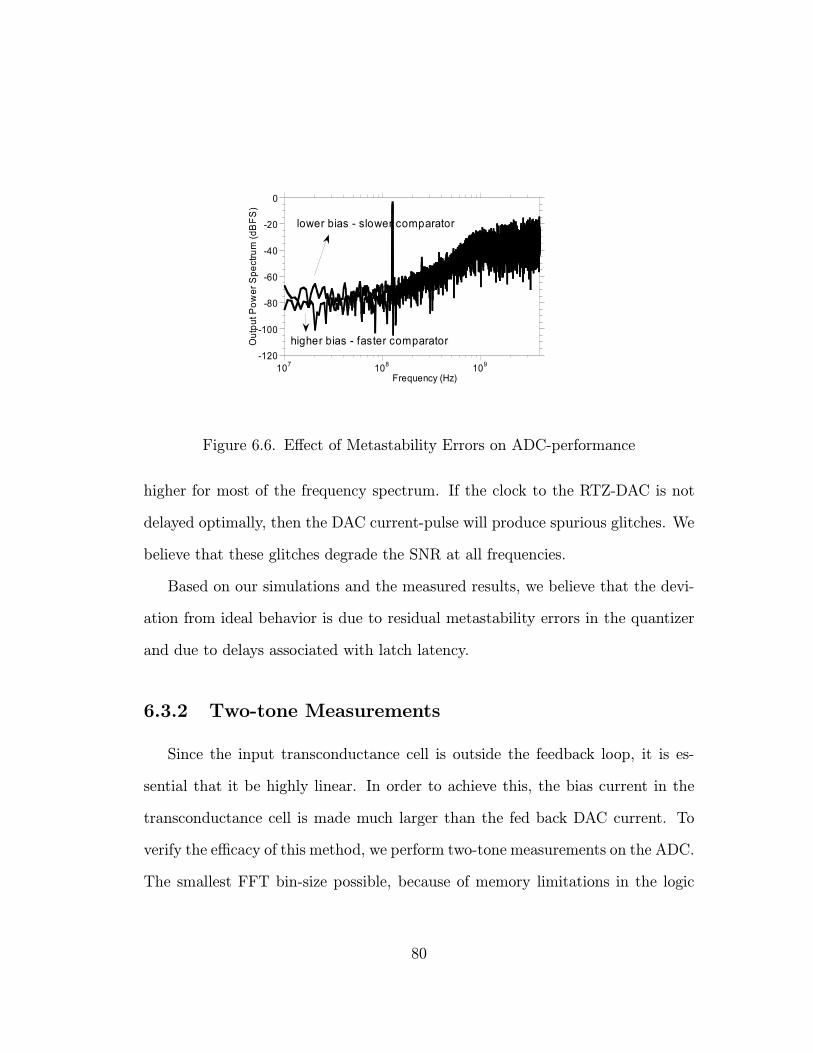
-120
-100
-80
-60
-40
-20
0
107 108 109
Out
put P
ower
Spe
ctru
m (d
BFS
)
Frequency (Hz)
lower bias - slower comparator
higher bias - faster comparator
Figure 6.6. Effect of Metastability Errors on ADC-performance
higher for most of the frequency spectrum. If the clock to the RTZ-DAC is not
delayed optimally, then the DAC current-pulse will produce spurious glitches. We
believe that these glitches degrade the SNR at all frequencies.
Based on our simulations and the measured results, we believe that the devi-
ation from ideal behavior is due to residual metastability errors in the quantizer
and due to delays associated with latch latency.
6.3.2 Two-tone Measurements
Since the input transconductance cell is outside the feedback loop, it is es-
sential that it be highly linear. In order to achieve this, the bias current in the
transconductance cell is made much larger than the fed back DAC current. To
verify the efficacy of this method, we perform two-tone measurements on the ADC.
The smallest FFT bin-size possible, because of memory limitations in the logic
80

-100
-80
-60
-40
-20
0
106 107 108 109
Out
put P
ower
Spe
ctru
m (d
BFS)
Frequency (Hz)
RTZ DAC, 3ps clock delay
RTZ DAC, no clock delay
Figure 6.7. Effect of Latch Latency on the Output Power Spectrum
analyzer, is 60 kHz. For this reason, we use a spacing of 2 MHz between the two
tones.
Fig. 6.8 shows the output power spectrum for two tones at 124 and 126 MHz.
We observe > 80 dBc suppression of the two-tone intermodulation products. For
this measurement, the comparator was not biased for maximum speed. Due to
a design oversight, we do not use separate voltage sources for the integrator, the
comparator and the DAC. For this reason, the bias current in the DAC increases
at a much faster rate than the bias current in the integrator, when the supply-
voltage is increased. Hence, we observe only 70 dBc suppression of the two-tone
intermodulation products at the best bias-point (Fig. 6.9).
Based on these results, we conclude that, at the cost of increased DC power,
sufficient intermodulation suppression can be achieved by ensuring that the input
stage overloads well after loop-overload occurs. The discussion on the design and
the measured results of the ADC is now complete. In the following chapter, we
81
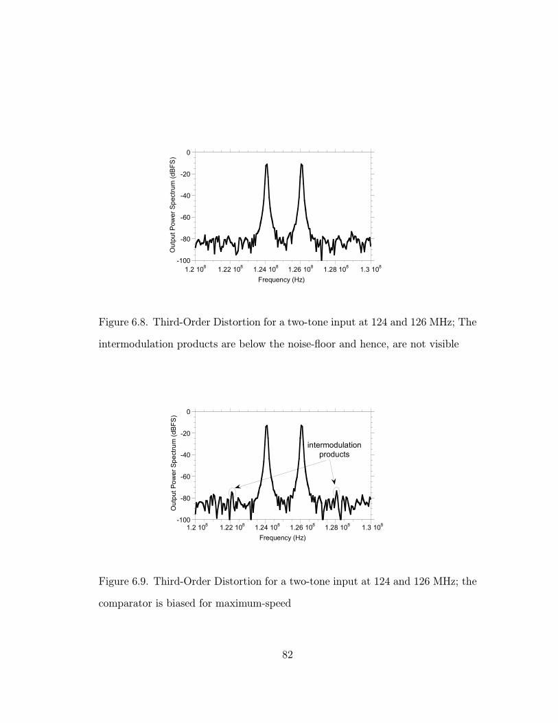
-100
-80
-60
-40
-20
0
1.2 108 1.22 108 1.24 108 1.26 108 1.28 108 1.3 108
Out
put P
ower
Spe
ctru
m (d
BFS
)
Frequency (Hz)
Figure 6.8. Third-Order Distortion for a two-tone input at 124 and 126 MHz; The
intermodulation products are below the noise-floor and hence, are not visible
-100
-80
-60
-40
-20
0
1.2 108 1.22 108 1.24 108 1.26 108 1.28 108 1.3 108
Out
put P
ower
Spe
ctru
m (d
BFS)
Frequency (Hz)
intermodulationproducts
Figure 6.9. Third-Order Distortion for a two-tone input at 124 and 126 MHz; the
comparator is biased for maximum-speed
82

present a summary of our results and suggest some ideas for future work.
83

Chapter 7
Conclusions and Future Work
7.1 Summary of achievements
In this work, we have demonstrated DHBTs using a substrate-transfer process
as well as using a conventional mesa-HBT process. In developing these process
technologies, we have had to either solve, or mitigate the effect of, several process
related problems including collector attack during substrate removal, base-emitter
electrical shorts, and interconnect-metal electrical shorts. The device results
demonstrated in this work are (i) a device with 165 GHz ftau and 300 GHz fmax
in a substrate-transfer process, (ii) a device with 215 GHz ftau and 210 GHz fmax
in a substrate-transfer process, and (iii) a device with 200 GHz ftau and 205 GHz
fmax in a narrow-mesa process. We have also developed a microstrip-based IC
wiring environment for the mesa-HBT process and the process-technology is now
capable of reliably yielding ICs with a complexity of 100 transistors.
We have designed, fabricated and tested a ECL-based static frequency divider
84
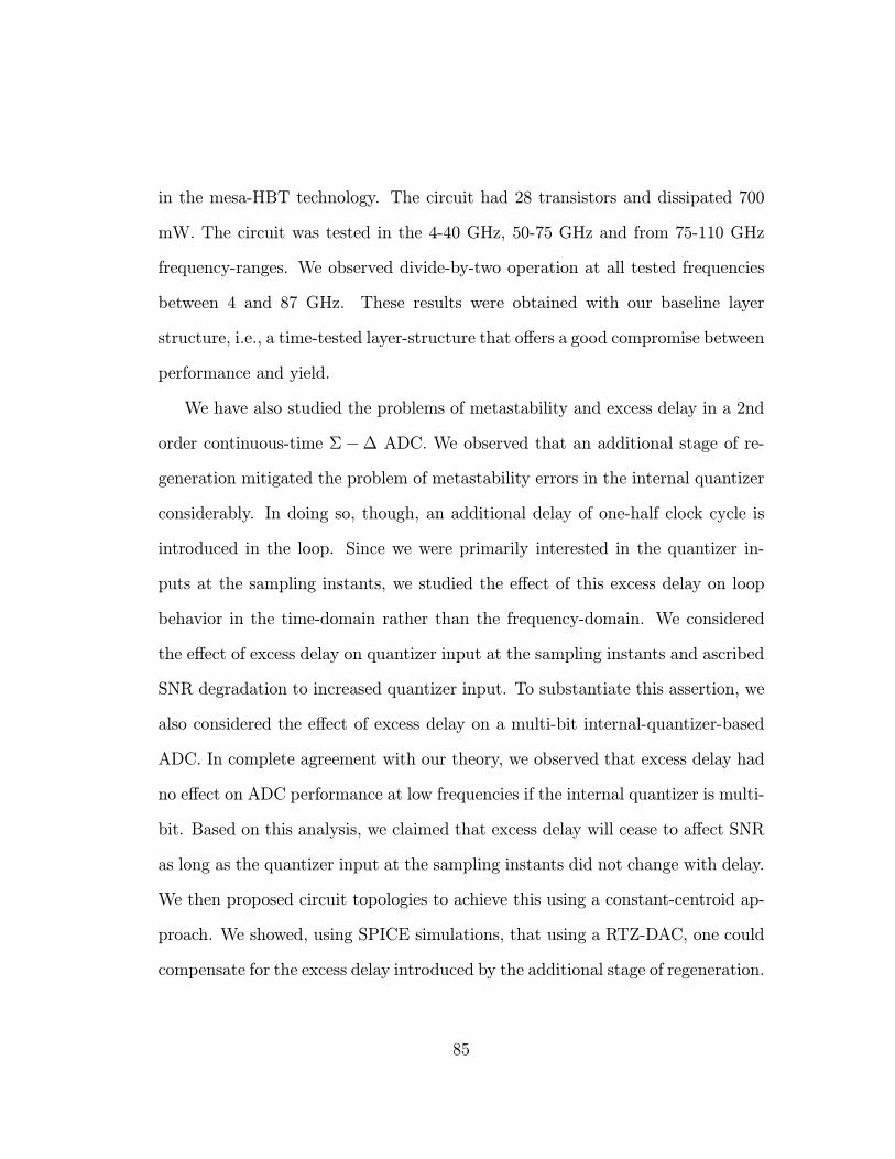
in the mesa-HBT technology. The circuit had 28 transistors and dissipated 700
mW. The circuit was tested in the 4-40 GHz, 50-75 GHz and from 75-110 GHz
frequency-ranges. We observed divide-by-two operation at all tested frequencies
between 4 and 87 GHz. These results were obtained with our baseline layer
structure, i.e., a time-tested layer-structure that offers a good compromise between
performance and yield.
We have also studied the problems of metastability and excess delay in a 2nd
order continuous-time Σ−∆ ADC. We observed that an additional stage of re-
generation mitigated the problem of metastability errors in the internal quantizer
considerably. In doing so, though, an additional delay of one-half clock cycle is
introduced in the loop. Since we were primarily interested in the quantizer in-
puts at the sampling instants, we studied the effect of this excess delay on loop
behavior in the time-domain rather than the frequency-domain. We considered
the effect of excess delay on quantizer input at the sampling instants and ascribed
SNR degradation to increased quantizer input. To substantiate this assertion, we
also considered the effect of excess delay on a multi-bit internal-quantizer-based
ADC. In complete agreement with our theory, we observed that excess delay had
no effect on ADC performance at low frequencies if the internal quantizer is multi-
bit. Based on this analysis, we claimed that excess delay will cease to affect SNR
as long as the quantizer input at the sampling instants did not change with delay.
We then proposed circuit topologies to achieve this using a constant-centroid ap-
proach. We showed, using SPICE simulations, that using a RTZ-DAC, one could
compensate for the excess delay introduced by the additional stage of regeneration.
85

We fabricated and tested two different ADC designs, one with a NRZ-DAC
and the other with a RTZ-DAC. The ADCs were measured using an analog spec-
trum analyzer-based technique as well as a logic analyzer-based digital-acquisition
technique. In agreement with our simulations, we observed that the RTZ-DAC-
based ADC showed better resolution than the NRZ-DAC-based ADC. We believe
that this is due to the former’s reduced loop delay. We used the digital acqui-
sition technique to perform both one-tone and two-tone measurements on the
RTZ-DAC-based ADC. We observed that comparator speeds 10 : 1 higher than
the clock-rate, and optimum clock delay for the RTZ-DAC are required to obtain
ideal resolution. We also performed two-tone measurements on the ADC to mea-
sure the linearity of the input stage. Due to a design oversight, we were unable
to independently control the bias currents on the integrator and the RTZ-DAC.
Hence, we noticed a degradation in intermodulation-suppression as we increased
the comparator speed (bias-voltage). We observed > 80 dBc intermodulation-
suppression at the lowest bias point and 70 dBc intermodulation-suppression at
the highest bias point.
7.2 Future Work
Most of the results in this work were achieved after long periods of frustration
in the clean room. Even though the final results have been impressive, and will
continue to be, given the nature of the technology, the author feels that continued
student frustration might be too high a price to pay for it. Considering that these
circuits are fabricated in a university clean room, it might be advisable to limit
86

the circuit complexity to less than 100 HBTs.
A couple of process related problems still remain and will have to be solved in
order to improve the yield on ICs. A large number of interconnect-metal electrical-
shorts were observed and is believed to be due to large pin-hole density in the SiN
dielectric layer. Other members of the group have also observed this problem
and the SiN dielectric-layer process has to be recharacterized. As an alternative,
SiO2 can also be used as the dielectric layer for MIM capacitors. In addition,
we also noticed several instances of base-emitter electrical shorts. Although one
would expect instances of electrical shorts in a self-aligned process, the self-aligned
nature of the process, in itself, is incapable of generating the frequency of electrical
short occurences observed. A detailed study of the base-emitter wet-etch process
might help find causes for, and solve the problem of, base-emitter electrical shorts.
In order to improve the logic-speed of the technology, a change in HBT layer-
structure is necessary. Using a 300A C-doped InGaAs base, M. Dahlstrom has
recently demonstrated a device with 280 GHz fτ and 440 GHz fmax [8]. The high
fτ , fmax and Current-density to capacitance ratio, and the low emitter-resistivity
make this an attractive choice for designing logic circuits. Designs based on such
a device model are currently in fabrication and should result in divide-by-two
operation at higher frequencies.
87
Bibliography
[1] U. Bhattacharya, L. Samoska, R. Pullela, J. Guthrie, Q. Lee, B. Agarwal,
D. Mensa, M. J. W. Rodwell, “170 GHz transferred-substrate heterojunction
bipolar transistor”, IEE Electronics Letters, vol 32, (no. 15), pp. 1405-6, July
1996
[2] Y. Betser, D. Scott, D. Mensa, S. Jaganathan, T. Mathew, M. J. W. Rodwell,
“InAlAs/InGaAs HBTs with simultaneously high values of fτ and fmax for
mixed analog/digital applications”, IEEE Electron Device Letters, vol. 22,
(no. 2), pp. 56-8, Feb. 2001
[3] R. Caprio, “Precision differential voltage-current convertor”, IEE Electronics
Letters, vol. 9, (no. 6), pp. 147-8, Mar. 1973
[4] K. T. Chan, K. W. Martin, “Components for a GaAs delta-sigma modulator
oversampled analog-to-digital converter”, 1992 International Symposium on
Circuits and Systems, pp. 1300-3, San Diego, CA, USA, May 1992
[5] E. M. Cherry, D. E. Hooper, “Amplifying devices and low-pass amplifier
design”, John Wiley and Sons, 1968
88
[6] J. A. Cherry, W. M. Snelgrove and P. Schvan, “Signal-dependent timing
jitter in continuous-time Σ∆ modulators”, IEE Electronics Letters, vol. 33,
(no. 13), pp. 1118-9, 19 June 1997
[7] J. A. Cherry, W. M. Snelgrove, “Excess Loop Delay in Continuous-Time
Delta-Sigma Modulators”, IEEE Transactions on Circuits and Systems-II :
Analog and Digital Signal Processing, vol. 46, (no. 4), pp. 376-89, Apr. 1999
[8] M. Dahlstrom, M. Urteaga, S. Krishnan, N. Parthasarathy, M. J. W. Rod-
well, X. M. Fang, D. Lubyshev, Y. Wu, J. M. Fastenau and W. K. Liu,
“Ultra-Wideband DHBTs using a Graded Carbon-Doped InGaAs base”, post-
deadline news, IPRM 2002, Stockholm, Sweden, May 2002
[9] M. W. Dvorak, C. R. Bolognesi, O. J. Pitts and S. P. Watkins, “300 GHz
InP/GaAsSb/InP double HBTs with high current capability and BVCEO >
6V”, IEEE Electron Device Letters, vol 22, (no. 8), pp. 361-3, Aug. 2001
[10] R. M. Gray, “Oversampled sigma-delta modulation ”, IEEE Transactions on
Communication, vol 35, (no. 5), pp. 481-9, May 1987
[11] J. R. Guthrie, M. Urteaga, D. Scott, D. Mensa, T. Mathew, Q. Lee, S. Kr-
ishnan, S. Jaganathan, Y. Betser and M. Rodwell, “HBT MMIC 75 GHz
power amplifiers ”, 2000 IEEE Conference on Indium Phosphide and Related
Materials, Williamsburg, May 2000
[12] J. R. Guthrie, “ Metal Substrate Process and W-band Power Amplifier In-
89
tegrated Circuits in Transferred-Substrate HBT Technology ”, Ph. D. thesis,
UC Santa Barbara, Dec. 1999
[13] J. Harrison, N. Weste, “Analytic limitations on Sigma-Delta Modulator Per-
formance”, 2000 International Symposium on Circuits and Systems, pp. 746-
9, Geneva, Switzerland, May 2000
[14] U. Horbach, “Design of a 20-bit sigma-delta A/D-converter for audio applica-
tions”, 1990 International Symposium on Circuits and Systems, pp. 2789-92,
New Orleans, LA, USA, May 1990
[15] M. Ida, K. Kurishima, N. Watanabe, T. Enoki, “InP/InGaAs DHBTs with
341-GHz fτ at high current density of over 800 kA/cm2”, International Elec-
tron Devices Meeting 2001, pp. 35.4.1-4, Washington DC, USA, Dec. 2001
[16] S. Jaganathan, S. Krishnan, D. Mensa, T. Mathew, Y. Betser, Y. Wei,
D. Scott, M. Urteaga and M. J. W. Rodwell, “An 18 GHz Continuous-Time
Σ−∆ Analog-Digital Converter Implemented in InP-Transferred Substrate
HBT Technology”,IEEE Journal of Solid State Circuits, vol 36, no. 9, pp.
1343-50, September 2001
[17] B. Jaganathan, M. Khater, F. Pagette, J. -S. Rieh, D. Angell, H. Chen,
J. Florkey, F. Golan, D. R. Greenberg, R. Groves, S. J. Jeng, J. Johnson,
E. Mengistu, K. T. Schonenberg, C. M. Schnabel, P. Smith, A. Stricker,
D. Ahlgren, G. Freeman, K. Stein and S. Subbanna, “Self-Aligned SiGe NPN
Transistors with 285 GHz fmax and 207 GHz fτ in a Manufacturable Technol-
ogy”, IEEE Electron Device Letters, vol. 23, no. 5, pp. 258-260, May 2002
90
[18] S. Jaganathan, “18-GHz clock-rate delta-sigma oversampled ADCs in the
transferred-substrate HBT process”, Ph. D. thesis, UC Santa Barbara, Sep.
2000
[19] S. J. Jeng, B. Jaganathan, J. S. Rieh, J. Johnson, K. T. Schonenberg,
D. Greenberg, A. Stricker, H. Chen, M. Khater, D. Ahlgren, G. Freeman,
K. Stein, S. Subbanna, “A 210-GHz fτ SiGe HBT with a non-self-aligned
structure”, IEE Electron Device Letters, vol 22, (no. 11), pp. 542-4, Nov.
2001
[20] J. F. Jensen, G. Raghavan, A. E. Cosand, R. H. Walden, “A 3.2-GHz second-
order delta-sigma modulator implemented in InP HBT technology”, IEEE
Journal of Solid State Circuits, vol. 30, (no. 10), pp. 1119-27, Oct. 1995.
[21] C. T. Kirk, “A theory of transistor cutoff frequency(fT ) fall-off at high current
density”, IEEE Transactions on Electron Devices, ED-9, p. 164, 1962
[22] S. Krishnan, S. Jaganathan, T. Mathew, Y. Wei, M. J. W. Rodwell, “Broad-
band HBT amplifiers”, 2000 IEEE Cornell Conference on High Speed Elec-
tronics, Aug. 2000
[23] S. Krishnan, D. Mensa, J. Guthrie, S. Jaganathan, T. Mathew, R. Girish,
Y. Wei and M. J. W. Rodwell, “ Broadband lumped HBT amplifiers ”, IEE
Electronics Letters, vol 36, no. 5, pp 466-7, Mar. 2000
[24] Q. Lee, S. C. Martin, D. Mensa, R. P. Smith, J. Guthrie and M. J. W. Rod-
91

well, “Submicron transferred-substrate heterojunction bipolar transistors”,
IEEE Electron Device Letters, vol. 20, no. 8, pp. 396-8, Aug. 99
[25] Q. Lee, D. Mensa, J. Guthrie, S. Jaganathan, T. Mathew, Y. Betser, S. Kr-
ishnan, S. Ceran, M. J. W. Rodwell, “66 GHz static frequency divider in
transferred-substrate HBT technology”, 1999 IEEE Radio Frequency Inte-
grated Circuits Symposium, Anaheim, CA, USA, pp. 87-90, June 1999
[26] T. Mathew, S. Jaganathan, D. Scott, S. Krishnan, Y. Wei, M. Urteaga,
M. J. W. Rodwell and S. Long, “ 2-bit adder: carry and sum logic circuits at
19 GHz clock frequency in InAlAs/InGaAs HBT technology”, IEE Electronics
Letters, vol 37, no. 19, pp. 1156-7, Sep. 2001
[27] T. Mathew, H. J. Kim, D. Scott, S. Jaganathan, S. Krishnan, Y. Wei,
M. Urteaga, S. Long, M. J. W. Rodwell, “75 GHz ECL static frequency
divider using InAlAs/InGaAs HBTs”, IEE Electronics Letters, vol. 37, (no.
11), pp. 667-8, May 2001
[28] T. Mathew, “High-Speed Digital ICs in Transferred-Substrate HBT Technol-
ogy”, Ph. D. thesis, UC Santa Barbara, Sep. 2001
[29] D. Mensa, “Improved Current-Gain Cutoff Frequency and High Gain-
Bandwidth Amplifiers in Transferred-Substrate HBT Technology”, Ph. D.
Thesis, UC Santa Barbara, Sep. 1999
[30] S. R. Norsworthy, R. S. Schreier, G. C. Temes, “Delta-Sigma Data Convert-
ers: Theory, Design and Simulation”, IEEE Press, 1997
92

[31] C. Nguyen, T. Liu, M. Chen, R. Virk, M. Chen, “Bandgap engineered InP-
based power double heterojunction bipolar transistors”, 1997 International
Conference on Indium Phosphide and Related Materials, Cape Cod, MA,
USA, pp. 15-19, 1997
[32] E. Ohue, R. Hayami, K. Oda, H. Shimamoto, K. Washio, “5.3-ps ECL and
71-GHz static frequency divider in self-aligned SEG SiGe HBT”, Proceedings
of the 2001 Bipolar/BiCMOS Circuits and Technology Meeting, Minneapolis,
MN, USA, pp. 26-9, Oct. 2001
[33] B. Razavi, “Principles of data conversion system design”, New York, IEEE
Press, 1995
[34] M. J. W. Rodwell, M. Urteaga, Y. Betser, T. Mathew, S. Krishnan, D. Scott,
S. Jaganathan, D. Mensa, J. Guthrie, R. Pullela, Q. Lee, B. Agarwal,
U. Bhattacharya, S. Long, S. C. Martin and R. P. Smith, “Scaling of In-
GaAs/InAlAs HBTs for High Speed Mixed-Signal and mm-Wave ICs”, In-
ternational Journal of High Speed Electronics and Systems, vol. 11, (no. 1),
pp. 159-216, 2001
[35] M. Sokolich, C. H. Fields, S. Thomas III, Binqiang Shi, Y. K. Boegeman,
R. Martinez, A. R. Kramer, M. Madhav, “A low-power 72.8-GHz static fre-
quency divider in AlInAs/InGaAs HBT technology”, IEEE Journal of Solid-
State Circuits, vol. 36, (no. 9), pp. 1328-1334, Sep. 2001
[36] M. Urteaga, D. Scott, T. Mathew, S. Krishnan, Y. Wei and M. J. W. Rodwell,
“Single-stage G-band HBT amplifier with 6.3 dB gain at 175 GHz ”, IEEE
93
Gallium Arsenide Integrated Circuit Symposium, 2001, Baltimore, MD, pp.
83-87
[37] R. S. Virk, M. Y. Chen, C. Nguyen, T. Liu, M. Matloubian, D. B. Rensch,
“A high-performance AlInAs/InGaAs/InP DHBT K-band power cell”, IEEE
Microwave and Guided Wave Letters, vol 7, (no. 10), pp. 323-5, Oct. 1997
[38] K. Washio, “Self-aligned Si BJT/SiGe HBT Techonology and Its Applica-
tion”, International Journal of High Speed Electronics and Systems , Vol. 11,
No. 1 (2001) pp. 77-114
94

Appendix A
Process Flow
A.1 Focus check with 2” Si wafer
A Solvent Cleaning
1. Check the resistivity of the D.I. water. It should be > 17 MΩ.
2. Set spinner at 4 krpm, 2 minutes.
3. Get 2” Si wafer from drybox (in old toluene petri dish).
4. Start wafer spinning, then squirt with acetone.
5. Don’t let it dry, squirt with ISO, then ACE and ISO again.
6. Put on 200C hot plate for 5 minutes.
B Photoresist Application and Exposure
1. Cool down after dehydration, 5 min.
2. Wafer on spinner chuck with vacuum, blow with N2.
3. Apply SPR 950-0.8 with syringe and filter to cover wafer.
95

4. Spin at 2.5 krpm for 30 sec.
5. Soft Bake, 90C, 1 min. on hot plate.
6. Apply CEM with syringe and filter to cover wafer.
7. Spin at 4 krpm for 30 sec.
8. Use “Smartset Array” mask plate, run job as follows: ”FOCUS
SFOC2\FOC”, note down the best focus number returned by com-puter.
Align emitters perpendicular to the major flat of the wafer
A.2 Emitter Contacts (Mask Layer 1)
A Solvent Cleaning
1. Check the resistivity of the D.I. water. It should be > 17 MΩ.
2. Cold ACE 3 min.
3. Hot METH 3 min.
4. Hot ISO 3 min.
5. Running DI 3 min.
6. Blow dry with N2.
7. Dehydration bake, 120C, 30 min in petri dish without cover.
B Photoresist Application and Exposure
1. Cool down after dehydration, 5 min.
2. Wafer on spinner chuck with vacuum, blow with N2.
3. Apply SPR 950-0.8 with syringe and filter to cover wafer.
96
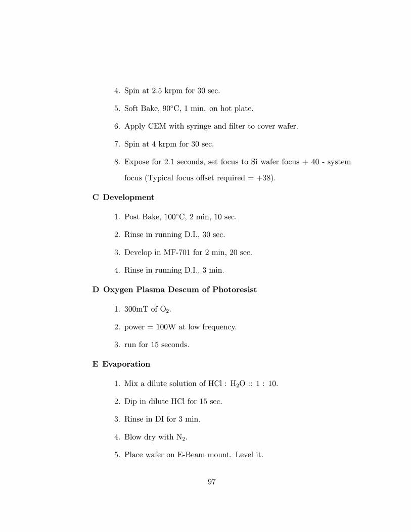
4. Spin at 2.5 krpm for 30 sec.
5. Soft Bake, 90C, 1 min. on hot plate.
6. Apply CEM with syringe and filter to cover wafer.
7. Spin at 4 krpm for 30 sec.
8. Expose for 2.1 seconds, set focus to Si wafer focus + 40 - system
focus (Typical focus offset required = +38).
C Development
1. Post Bake, 100C, 2 min, 10 sec.
2. Rinse in running D.I., 30 sec.
3. Develop in MF-701 for 2 min, 20 sec.
4. Rinse in running D.I., 3 min.
D Oxygen Plasma Descum of Photoresist
1. 300mT of O2.
2. power = 100W at low frequency.
3. run for 15 seconds.
E Evaporation
1. Mix a dilute solution of HCl : H2O :: 1 : 10.
2. Dip in dilute HCl for 15 sec.
3. Rinse in DI for 3 min.
4. Blow dry with N2.
5. Place wafer on E-Beam mount. Level it.
97

6. Put in a new crystal. A new crystal should always be used for
emitters.
7. Pump down to below 1 x 10⁻⁶ torr.
8. Deposit material:
Material Thickness(A) Dep. Rate (A/sec)Ti 200 1-2Pt 500 1Au 8000 15
(use the small crucible for Au - be sure to load the right amount
of charge. If charge is less Au might run out before the desired
thickness is reached and if it is more then it might spill out of the
crucible while melting.)
F Liftoff —>> DO NOT LET ACE DRY ON WAFER! <<—
1. Soak wafer in beaker of ACE until metal comes loose.
2. If the liftoff is stubborn, leave the wafer soaking in ACE overnight.
Because ACE evaporates quickly, seal the top of the beaker with
foil.
3. ACE squirt bottle. Do not squirt except at edges of wafer and only
with wafer immersed in acetone. Do not squirt hard.
4. Rinse with METH then ISO (squirt bottle).
5. Rinse in running DI water for 3 min.
6. Blow dry with N2.
7. Check under microscope, then Dektak thickness of metal.
98
A.3 Base Contact etch (no mask required)
A Oxygen Plasma Descum
1. 300mT of O2.
2. power = 100W at low frequency.
3. run for 15 seconds.
B Surface Prep
1. Mix a dilute solution of NH4OH : H2O :: 1 : 10
2. Dip in dilute NH4OH for 10 sec.
3. Rinse in DI for 3 min.
4. Blow dry with N2.
C InGaAs Emitter-cap Wet Etch
1. Mix a solution of H2O2 : H3PO4 : H2O :: 1 : 1 : 25
2. Etch for 25 seconds
3. Dektak to make sure that the etch depth is about 300A.
D InP Emitter Wet Etch
1. Mix a solution of HCl : H2O :: 1 : 4
2. Etch for 25 seconds
3. Dektak to make sure that the etch depth has increased by about
1200A
E Nonselective etch
99

1. Mix etchant as follows: 55ml of 1M citric acid in 220ml DI. Mix
well. Add 5ml H2O2. Mix well. Add 1ml Phosphoric acid. Mix
well.
2. Stirring at 200 rpm etch for 35 seconds by suspending the wafer in
a basket.
3. Rinse in DI for 3 min.
4. Blow dry with N2.
5. You should have etched ∼ 300 A of semiconductor or ∼ 100 A intothe base.
A.4 Base Contact (Mask Layer 2)
A Dehydration bake, 120C, 30 min. in petri dish without cover
B Photoresist Application and Exposure
1. Cool down after dehydration, 5 min.
2. Wafer on spinner chuck with vacuum, blow with N2.
3. Apply EIR 5214 with syringe and filter to cover wafer.
4. Spin at 6 krpm for 30 sec.
5. Hot Plate Bake, 95C, 1 min.
6. Expose for 0.32 sec., focus offset of 24.
7. Hot Plate Bake, 110C, 1min.
8. Flood Expose at 7.5 mW/cm2 for 30 sec.
C Development
100
1. Develop in MF-701 for 30 sec.
2. Rinse in running DI water for 3 min.
3. Blow dry with N2.
4. Observe under microscope. If there is a suspicion that some pho-
toresist is remaining may go back into developer for 5 - 10 secs
longer.
D Oxygen Plasma Descum of Photoresist
1. Ozone UV photo reactor
2. load sample in the reactor
3. run for 10 minutes
E Evaporation
1. Mix a dilute solution of NH4OH : H2O :: 1 : 10
2. Dip in dilute NH4OH for 15 sec.
3. No DI Rinse
4. Blow dry with N2.
5. Place wafer on E-Beam mount. Level it.
6. Put in a new crystal. A new crystal should always be used for
emitters.
7. Pump down to below 1 x 10⁻⁶ torr.
8. Deposit material:
F Liftoff —>> DO NOT LET ACE DRY ON WAFER! <<—
101

Material Thickness(A) Dep. Rate (A/sec)Pd 30 1-2Ti 200 1-2Pt 400 1-2Au 350 3-5
1. Soak wafer in beaker of ACE until metal comes loose.
2. If the liftoff is stubborn, leave the wafer soaking in ACE overnight.
Because ACE evaporates quickly, seal the top of the beaker with
foil.
3. ACE squirt bottle. Do not squirt except at edges of wafer and only
with wafer immersed in acetone. Do not squirt hard.
4. Rinse with METH then ISO (squirt bottle).
5. Rinse in running DI water for 3 min.
6. Blow dry with N2.
7. Check under microscope, then Dektak thickness of metal.
G RTA for 60 seconds at 300C; program 300/1’p. Run a test
program first.
A.5 Base Plug (Mask Layer 3)
A Solvent Cleaning
1. Check the resistivity of the D.I. water. It should be > 17 MΩ.
2. Cold ACE 3 min.
3. Hot METH 3 min.
102

4. Hot ISO 3 min.
5. Running DI 3 min.
6. Blow dry with N2.
7. Dehydration bake, 120C, 30 min in petri dish without cover.
B Photoresist Application and Exposure
1. Cool down after dehydration, 5 min.
2. Wafer on spinner chuck with vacuum, blow with N2.
3. Apply EIR 5214 with syringe and filter to cover wafer.
4. Spin at 4 krpm for 30 sec.
5. Hot Plate Bake, 95C, 1 min.
6. Expose for 0.38 sec., focus offset of 24.
7. Hot Plate Bake, 110C, 1min.
8. Flood Expose at 7.5 mW/cm2 for 30 sec.
C Development
1. Develop in MF-701 for 40 sec.
2. Rinse in running DI water for 3 min.
3. Blow dry with N2.
4. Observe under microscope. If there is a suspicion that some pho-
toresist is remaining may go back into developer for 5 - 10 secs
longer.
D Oxygen Plasma Descum of Photoresist
103
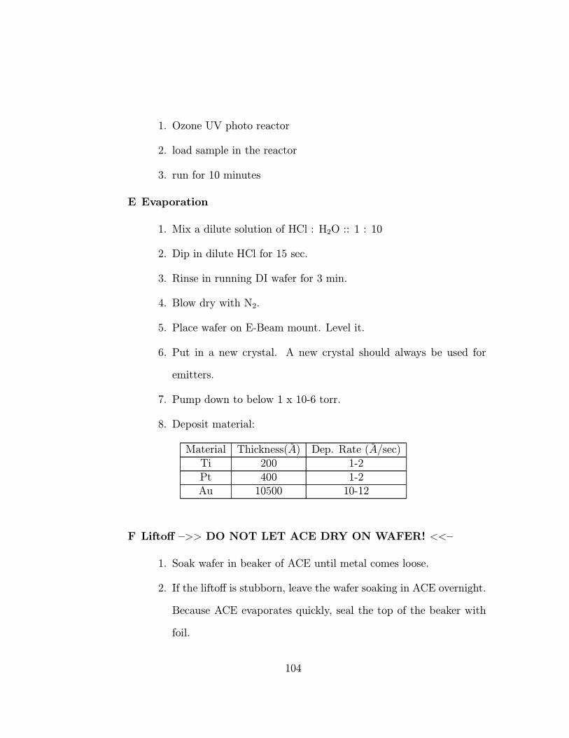
1. Ozone UV photo reactor
2. load sample in the reactor
3. run for 10 minutes
E Evaporation
1. Mix a dilute solution of HCl : H2O :: 1 : 10
2. Dip in dilute HCl for 15 sec.
3. Rinse in running DI wafer for 3 min.
4. Blow dry with N2.
5. Place wafer on E-Beam mount. Level it.
6. Put in a new crystal. A new crystal should always be used for
emitters.
7. Pump down to below 1 x 10⁻⁶ torr.
8. Deposit material:
Material Thickness(A) Dep. Rate (A/sec)Ti 200 1-2Pt 400 1-2Au 10500 10-12
F Liftoff —>> DO NOT LET ACE DRY ON WAFER! <<—
1. Soak wafer in beaker of ACE until metal comes loose.
2. If the liftoff is stubborn, leave the wafer soaking in ACE overnight.
Because ACE evaporates quickly, seal the top of the beaker with
foil.
104

3. ACE squirt bottle. Do not squirt except at edges of wafer and only
with wafer immersed in acetone. Do not squirt hard.
4. Rinse with METH then ISO (squirt bottle).
5. Rinse in running DI water for 3 min.
6. Blow dry with N2.
7. Check under microscope, then Dektak thickness of metal.
A.6 Base-Mesa Isolation (Mask Layer 4)
A Solvent Cleaning
1. Check the resistivity of the D.I. water. It should be > 17 MΩ.
2. Cold ACE 3 min.
3. Hot METH 3 min.
4. Hot ISO 3 min.
5. Running DI 3 min.
6. Blow dry with N2
7. Dehydration bake, 120C, 30 min. in petri dish without cover.
B Photoresist Application and Exposure
1. Cool down after dehydration, 5 min.
2. Wafer on spinner chuck with vacuum, blow with N2.
3. Apply SPR 518-A with syringe and filter to cover wafer.
4. Spin at 4.0 krpm for 30 sec.
5. Hot Plate Bake, 90C, 1 minute.
105
6. Expose for 0.8 sec, focus offset of 20.
7. Hot Plate Bake, 110C, 1 minute.
C Development
1. Develop in full beaker of MF-701 for 1 min, 30 seconds.
2. Rinse in running DI water for 3 min.
3. Blow dry with N2.
4. Observe under microscope. If there is a suspicion that some pho-
toresist is remaining may go back into developer for 5 - 10 secs
longer.
D Oxygen Plasma Descum of Photoresist and Hardbake
1. 300mT of O2.
2. power = 100W at low frequency.
3. run for 20 seconds.
E Base-Mesa Isolation Etch
1. Mix a solution of H2O2 : H3PO4 : H2O :: 1 : 1 : 25
2. Etch (the InGaAs base and InAlGaAs grade) for 35 seconds
3. Dektak to make sure that the etch depth is about 500A.
4. Mix a solution of HCl : H2O :: 1 : 4
5. Etch (the InP collector) for 25 seconds
6. Dektak to make sure that the etch depth has increased by about
1600A
106

F Resist strip
1. Remove photoresist with acetone in liftoff beaker for 3 minutes.
2. Rinse by spraying with METH and ISO.
3. Rinse in running DI water for 3 min.
4. Blow dry with N2.
G Oxygen Plasma Photoresist Removal (optional, at your discre-
tion)
1. 300mT of O2.
2. power = 100W at low frequency.
3. run for 30 seconds.
4. examine under microscope to ensure photoresist removal.
A.7 Collector Contacts (Mask Layer 5)
A Solvent Cleaning
1. Check the resistivity of the D.I. water. It should be > 17 MΩ.
2. Cold ACE 3 min.
3. Hot METH 3 min.
4. Hot ISO 3 min.
5. Running DI 3 min.
6. Blow dry with N2.
7. Dehydration bake, 120C, 30 min in petri dish without cover.
B Photoresist Application and Exposure
107
1. Cool down after dehydration, 5 min.
2. Wafer on spinner chuck with vacuum, blow with N2.
3. Apply EIR 5214 with syringe and filter to cover wafer.
4. Spin at 4 krpm for 30 sec.
5. Hot Plate Bake, 95C, 1 min.
6. Expose for 0.38 sec., focus offset of 24.
7. Hot Plate Bake, 110C, 1min.
8. Flood Expose at 7.5 mW/cm2 for 30 sec.
C Development
1. Develop in MF-701 for 40 sec.
2. Rinse in running DI water for 3 min.
3. Blow dry with N2.
4. Observe under microscope. If there is a suspicion that some pho-
toresist is remaining may go back into developer for 5 - 10 secs
longer.
D Oxygen Plasma Descum of Photoresist
1. Ozone UV photo reactor
2. load sample in the reactor
3. run for 10 minutes
E Evaporation
1. Mix a dilute solution of HCl : H2O :: 1 : 10
108

2. Dip in dilute HCl for 15 sec.
3. Rinse in running DI wafer for 3 min.
4. Blow dry with N2.
5. Place wafer on E-Beam mount. Level it.
6. Put in a new crystal. A new crystal should always be used for
emitters.
7. Pump down to below 1 x 10⁻⁶ torr.
8. Deposit material:
Material Thickness(A) Dep. Rate (A/sec)Ti 200 1-2Pt 400 1-2Au 4000 5-7
F Liftoff —>> DO NOT LET ACE DRY ON WAFER! <<—
1. Soak wafer in beaker of ACE until metal comes loose.
2. If the liftoff is stubborn, leave the wafer soaking in ACE overnight.
Because ACE evaporates quickly, seal the top of the beaker with
foil.
3. ACE squirt bottle. Do not squirt except at edges of wafer and only
with wafer immersed in acetone. Do not squirt hard.
4. Rinse with METH then ISO (squirt bottle).
5. Rinse in running DI water for 3 min.
6. Blow dry with N2.
109

7. Check under microscope, then Dektak thickness of metal.
A.8 Device Isolation (Mask Layer 6)
A Solvent Cleaning
1. Check the resistivity of the D.I. water. It should be > 17 MΩ.
2. Cold ACE 3 min.
3. Hot METH 3 min.
4. Hot ISO 3 min.
5. Running DI 3 min.
6. Blow dry with N2
7. Dehydration bake, 120C, 30 min. in petri dish without cover.
B Photoresist Application and Exposure
1. Cool down after dehydration, 5 min.
2. Wafer on spinner chuck with vacuum, blow with
N2.
3. Apply SPR 518-A with syringe and filter to cover wafer.
4. Spin at 4.0 krpm for 30 sec.
5. Hot Plate Bake, 90C, 1 minute.
6. Expose for 0.8 sec, focus offset of 20.
7. Hot Plate Bake, 110C, 1 minute.
C Development
1. Develop in full beaker of MF-701 for 1 min, 30 seconds.
110
2. Rinse in running DI water for 3 min.
3. Blow dry with N2.
4. Observe under microscope. If there is a suspicion that some pho-
toresist is remaining may go back into developer for 5 - 10 secs
longer.
D Oxygen Plasma Descum of Photoresist and Hardbake
1. 300mT of O2.
2. power = 100W at low frequency.
3. run for 20 seconds.
E Device Isolation Etch
1. Mix a solution of H2O2 : H3PO4 : H2O :: 1 : 1 : 25
2. Etch (the InGaAs sub-collector) for 20 seconds
3. Dektak to make sure that the etch depth is about 250A.
4. Mix a solution of HCl : H2O :: 1 : 4
5. Etch (the InP sub-collector and the InP buffer) for 30 seconds
6. Dektak to make sure that the etch depth has increased by about
1750A
7. Check Isolation by measuring leakage between two collector pads
F Resist strip
1. Remove photoresist with acetone in liftoff beaker for 3 minutes.
2. Rinse by spraying with METH and ISO.
111
3. Rinse in running DI water for 3 min.
4. Blow dry with N2.
G Oxygen Plasma Photoresist Removal (optional, at your discre-
tion)
1. 300mT of O2.
2. power = 100W at low frequency.
3. run for 30 seconds.
4. examine under microscope to ensure photoresist removal.
H Characterization of process so far.
1. Dektak etch depth, measure TLMs.
A.9 Poly Planarize (Mask Layer 7)
A Solvent Cleaning
1. Get Poly out of refrigerator, warm up for at least 2 hours!!
2. Check the resistivity of the D.I. water. It should be > 17MΩ.
3. Cold ACE 3 min.
4. Hot METH 3 min.
5. Hot ISO 3 min.
6. Running DI 3 min.
7. Blow dry with N2.
8. Dehydration bake, 120C, 30 min. in petri dish without cover.
B Poly Spin & Cure
112
1. Mix adhesion promoter in designated beaker (∼ 0.3 mL of VM-651from bottle using plastic dropper in 300 mL of D.I.). Stir then get
a new dropper.
2. Wafer on spinner chuck with vacuum, blow with N2.
3. Apply adhesion promoter to cover wafer.
4. Let it sit on the wafer for 20 seconds.
5. Spin at 3.0 krpm for 60 sec.
6. Hot plate bake, 125C, 3 minutes.
7. Apply DuPont Ployimide (PI 2556) to cover wafer with syringe
and 1 µm filter.
8. Let sit on wafer for 20 seconds.
9. Spin at 2.5 krpm for 30 sec (to give 1.8 µm film).
10. Hard bake polyimide in programmable oven as follows in petri
dish without cover, and with the base of the petri dish covered
with aluminum foil.(Alternate Option : Use the program P3 in the
BLUE-M OVEN used for BCB cure.)
(a) hold at 90C for 60 min.
(b) ramp at 4C per min. to 150C.
(c) hold at 150C for 60 min.
(d) ramp at 4C per min. to 230C.
(e) hold at 230C for 60 min.
(f) ramp at 4C per min. to 170C.
113

C Photoresist Application and Exposure
1. Remove from oven when below 50C.
2. Wafer on spinner chuck with vacuum, blow with N2.
3. Apply AZ 4330 with syringe and filter to cover wafer.
4. Spin at 5.0 krpm for 30 sec.
5. Soft Bake, 90C, 30 min. in petri dish without cover.
6. Hard Bake, 120C, 30 min. in petri dish without cover.
D Polyimide Etchback
1. Load RIE#1 according to instructions.
2. Pump down to low E-6.
3. Set up laser monitor.
(a) Look for diffraction pattern to identify beam. Laser signal
should be about 500mV. Use outermost spot of laser beam.
(b) Set up chart recorder for 1 hour and ∼700mV.
4. Etch conditions:
(a) O2 flow rate 7.0 sccm.
(b) chamber pressure = 10 mTorr.
(c) P=60W (control this watching Heathkit).
(d) Voltage should be around 350 V.
5. Etch for 17.5 cycles.
E Check
114

1. Load wafer in SEM and look at 1um emitter fingers to see if they
are clear.
2. If not, etch two minutes in PEII-A at 100W, 300 mT then SEM
again.
F Photoresist Application and Exposure
1. Wafer on spinner chuck with vacuum, blow with N2.
2. Apply SPR 518-A with syringe and filter to cover wafer.
3. Spin at 3.0 krpm for 30 sec.
4. Hot Plate Bake, 90C, 1 minute.
5. Expose for 1.1 sec, focus offset of +12. Must use global alignment.
6. Hot Plate Bake, 110C, 1 minute.
G Development
1. Develop in MF-701 for 1 min, 30 seconds.
2. Rinse in running D.I. for 3 minutes.
3. Flood Expose at 7.5 mW/cm2 for 2 minutes.
4. Hard Bake, 120C, 30 min. in petri dish without cover.
I Etch Poly Poly etch for 30 minutes, PEII-A, 300 mT O2, 100 W
J Resist strip
1. Remove resist in MF-701, 2 minutes.
2. Rinse in running D.I. for 3 minutes.
3. Blow dry with N2.
115

4. Inspect under microscope.
K Reflow Bake Hot plate bake, 250C, 10 minutes to reflow polyimide
and complete the cure.
A.10 NiCr Resistors (Mask Layer 8)
A Solvent Cleaning
1. Check the resistivity of the D.I. water. It should be > 17MΩ.
2. Cold ACE 3 min.
3. Hot METH 3 min.
4. Hot ISO 3 min.
5. Running DI 3 min.
6. Blow dry with N2.
7. Dehydration bake, 120C, 30 min. in petri dish without cover.
B Photoresist Application and Exposure
1. Cool down after dehydration, 5 min.
2. Wafer on spinner chuck with vacuum, blow with N2.
3. Apply EIR 5214 with syringe and filter to cover wafer.
4. Spin at 6 krpm for 30 sec.
5. Hot Plate Bake, 95C, 1 min.
6. Expose for 0.32 sec, focus offset of +18.
7. Hot Plate Bake, 110C, 1 min.
8. Flood Expose at 7.5 mW/cm2 for 30 sec.
116

C Development
1. Develop in MF-701 for 30 sec.
2. Rinse in running DI water for 3 min.
3. Blow dry with N2.
4. Observe under microscope. If there is a suspicion that some pho-
toresist is remaining may go back into developer for 5 - 10 secs
longer.
D Oxygen Plasma Descum of Photoresist
1. 300mT of O2.
2. power = 100W at low frequency.
3. run for 30 seconds.
E Evaporation
1. Mix a dilute solution of HCl : H2O :: 1 : 10.
2. Dip in dilute HCl for 45 sec.
3. Rinse in DI for 3 min.
4. Blow dry with N2.
5. Place wafer on E-Beam mount. Level it.
6. Put in a new crystal. A new crystal should always be used for
emitters.
7. Pump down to below 1 x 10⁻⁶ torr.
8. Deposit material:
117

Material Thickness(A) Dep. Rate (A/sec)Ti 25 1-2SiO2 500 1-2NiCr 420 0.7
F Liftoff —>> DO NOT LET ACE DRY ON WAFER! <<—
1. Soak wafer in beaker of ACE until metal comes loose.
2. If the liftoff is stubborn, leave the wafer soaking in ACE overnight.
Because ACE evaporates quickly, seal the top of the beaker with
foil.
3. ACE squirt bottle. Do not squirt except at edges of wafer and only
with wafer immersed in acetone. Do not squirt hard.
4. Rinse with METH then ISO (squirt bottle).
5. Rinse in running DI water for 3 min.
6. Blow dry with N2.
7. Check under microscope, then Dektak thickness of metal.
A.11 Pad Metal (Mask Layer 9)
A Solvent Cleaning
1. Check the resistivity of the D.I. water. It should be > 17MΩ.
2. Cold ACE 3 min.
3. Hot METH 3 min.
4. Hot ISO 3 min.
5. Running DI 3 min.
118

6. Blow dry with N2.
7. Dehydration bake, 120C, 30 min. in petri dish without cover.
B Photoresist Application and Exposure
1. Cool down after dehydration, 5 min.
2. Wafer on spinner chuck with vacuum, blow with N2.
3. Apply EIR 5214 with syringe and filter to cover wafer.
4. Spin at 4 krpm for 30 sec.
5. Hot Plate Bake, 95C, 1 min.
6. Expose for 0.38 sec, focus offset of 18.
7. Hot Plate Bake, 110C, 1 min.
8. Flood Expose at 7.5 mW/cm2 for 30 sec.
C Development
1. Develop in MF-701 for 40 sec.
2. Rinse in running DI water for 3 min.
3. Blow dry with N2.
4. Observe under microscope. If there is a suspicion that some pho-
toresist is remaining may go back into developer for 5 - 10 secs
longer.
D Oxygen Plasma Descum of Photoresist
1. 300mT of O2.
2. power = 100W at low frequency.
119

3. run for 15 seconds.
E Evaporation
1. Mix a dilute solution of HCl : H2O :: 1 : 10.
2. Dip in dilute HCl for 15 sec.
3. Rinse in DI for 3 min.
4. Blow dry with N2.
5. Put in a new crystal.
6. Pump down to below 1 x 10⁻⁶ torr.
7. Deposit material:
Material Thickness(A) Dep. Rate (A/sec)Ti 200 2-3Au 12000 12-15Ti 100 2-3
F Liftoff —>> DO NOT LET ACE DRY ON WAFER! <<—
1. Soak wafer in beaker of ACE until metal comes loose.
2. If the liftoff is stubborn, leave the wafer soaking in ACE overnight.
Because ACE evaporates quickly, seal the top of the beaker with
foil.
3. ACE squirt bottle. Do not squirt except at edges of wafer and only
with wafer immersed in acetone. Do not squirt hard.
4. Rinse with METH then ISO (squirt bottle).
5. Rinse in running DI water for 3 min.
120
6. Blow dry with N2.
7. Check under microscope, then Dektak thickness of metal.
A.12 SiN Etch (Mask Layer 10)
A Solvent Cleaning
1. Wipe lower electrode, housing of PECVD with ISO soaked
wipes. Careful, HOT!
2. Run 60CLNSiN.
3. Check the resistivity of the D.I. water. It should be > 17MΩ.
4. Cold ACE 3 min.
5. Hot METH 3 min.
6. Hot ISO 3 min.
7. Running DI 3 min.
8. Blow dry with N2
B SiN Deposition, PR application
1. Load wafer in PECVD, run SiN10. Remember orientation.
2. Unload, rinse with ISO beaker with ISO (of course) for 1 minute.
3. Load wafer in PECVD, rotate 120 from previous orientation, run
SiN20.
4. Unload, rinse with ISO beaker with ISO (of course) for 1 minute.
5. Load wafer in PECVD, rotate 120 from previous orientation, run
SiN10.
121
6. Unload, let wafer cool for 5 minutes.
7. Wafer on spinner chuck with vacuum, blow with N2.
8. Apply SPR 518-A with syringe and filter to cover wafer.
9. Spin at 4 krpm for 30 sec.
10. Hot Plate Bake, 90C, 1 min 15 seconds.
11. Expose for 0.9 sec, focus offset of 20.
12. Hot Plate Bake, 110C, 1 min 30 seconds.
C Development
1. Develop in full beaker of MF-701 for 1 min. 30 seconds.
2. Rinse in running DI water for 3 min.
3. Blow dry with N2.
4. Observe under microscope. If there is a suspicion that some pho-
toresist is remaining may go back into developer for 5 - 10 secs
longer.
D Oxygen Plasma Descum of Photoresist
1. 300mT of O2.
2. power = 100W at low frequency.
3. run for 20 seconds.
E SF6, O2, Ar RIE3
1. Clean system with ISO and clean wipes.
2. O2 clean of system as follows:
122

(a) O2 flow rate = 20.0 sccm.
(b) chamber pressure = 10.0 mTorr.
(c) Voltage=500 V.
(d) Minimize reflected power by tuning (Power should be ∼ 200W).
3. Load sample, pump down to at least 1 x 10⁻⁵ torr.
4. Etch conditions:
(a) SF6.,O2,Ar flow rate = 5.0, 3.0, 10.0 sccm
(b) chamber pressure = 20.0 mTorr.
(c) Voltage=250 V.
(d) Minimize reflected power by tuning (Power should be about 50
W).
(e) Etch for 6 minutes (This etches the SiO2 evaporated with
Metal-1).
5. Look under microscope. Etch in 1 min. increments if necessary.
F Resist strip
1. Remove photoresist with acetone in liftoff beaker for 3 minutes.
2. Rinse by spraying with METH and ISO.
3. Rinse in running DI water for 3 min.
4. Blow dry with N2.
G Oxygen Plasma Photoresist Removal (optional, at your discre-
tion)
123
1. 300mT of O2.
2. power = 100W at low frequency.
3. run for 30 seconds.
4. examine under microscope to ensure photoresist removal.
A.13 Metal 2 (Mask Layer 11)
A Solvent Cleaning
1. Check the resistivity of the D.I. water. It should be > 17MΩ.
2. Cold ACE 3 min.
3. Hot METH 3 min.
4. Hot ISO 3 min.
5. Running DI 3 min.
6. Blow dry with N2.
7. Dehydration bake, 120C, 30 min. in petri dish without cover.
B Photoresist Application and Exposure
1. Cool down after dehydration, 5 min.
2. Wafer on spinner chuck with vacuum, blow with N2.
3. Apply EIR 5214 with syringe and filter to cover wafer.
4. Spin at 4 krpm for 30 sec.
5. Hot Plate Bake, 95C, 1 min 15 seconds.
6. Expose for 0.38 sec, focus offset of 18.
7. Hot Plate Bake, 110C, 1 min 45 seconds.
124
8. Flood Expose at 7.5 mW/cm2 for 30 sec.
C Development
1. Develop in MF-701 for 40 sec.
2. Rinse in running DI water for 3 min.
3. Blow dry with N2.
4. Observe under microscope. If there is a suspicion that some pho-
toresist is remaining may go back into developer for 5 - 10 secs
longer.
D Oxygen Plasma Descum of Photoresist
1. 300mT of O2.
2. power = 100W at low frequency.
3. run for 15 seconds.
E Evaporation
1. Mix a dilute solution of HCl : H2O :: 1 : 10.
2. Dip in dilute HCl for 15 sec.
3. Rinse in DI for 3 min.
4. Blow dry with N2.
5. Place wafer on E-Beam mount for angle of about 30 and rotation.
6. Put in a new crystal.
7. Pump down to below 1 x 10⁻⁶ torr.
8. Deposit material:
125

Material Thickness(A) Dep. Rate (A/sec)Ti 200 2-3Au 9500 15Ti 100 2-3
F Liftoff —>> DO NOT LET ACE DRY ON WAFER! <<—
1. Soak wafer in beaker of ACE until metal comes loose.
2. If the liftoff is stubborn, leave the wafer soaking in ACE overnight.
Because ACE evaporates quickly, seal the top of the beaker with
foil.
3. ACE squirt bottle. Do not squirt except at edges of wafer and only
with wafer immersed in acetone. Do not squirt hard.
4. Rinse with METH then ISO (squirt bottle).
5. Rinse in running DI water for 3 min.
6. Blow dry with N2.
7. Check under microscope, then Dektak thickness of metal.
A.14 BCB (Mask Layer 12)
A Solvent Cleaning
1. Check the resistivity of the D.I. water. It should be > 17MΩ.
2. Cold ACE 3 min.
3. Hot METH 3 min.
4. Hot ISO 3 min.
5. Running DI 3 min.
126

6. Blow dry with N2
7. Dehydration bake, 120C, 30 min. in petri dish without cover
B BCB Spin & Cure
1. Turn N2 flow up to maximum (100 scfh) in BlueM oven.
2. Wafer on spinner chuck with vacuum, blow with N2.
3. Apply adhesion promoter AP-8000 with dropper to cover wafer.
4. Spin at 4.0 krpm for 30 sec.
5. Blow dry with N2.
6. Set spinner for 4500 RPM.
7. Apply BCB 57, spin at 4.5 krpm for 30 sec (To give 6 µm film).
8. Cure BCB in BlueM oven (Prog 2) in petri dish without cover, and
with the base of the petri dish covered with aluminum foil.
C Low temp. SiN deposition and PR application
1. Wipe lower electrode, housing of PECVD with ISO soaked
wipes. Careful, HOT!
2. Run 60CLNSiN.
3. Load the program kris s01 from the custom programs subdirec-
tory. SET TEMP for PECVD will change to 120. Wait for the
temperature to reach 120C.
4. Load wafer in PECVD, run kris s01 (approx. 80 min).
5. Unload the wafer and load the program 60CLNSiN. SET TEMP
goes back to 265C.
127
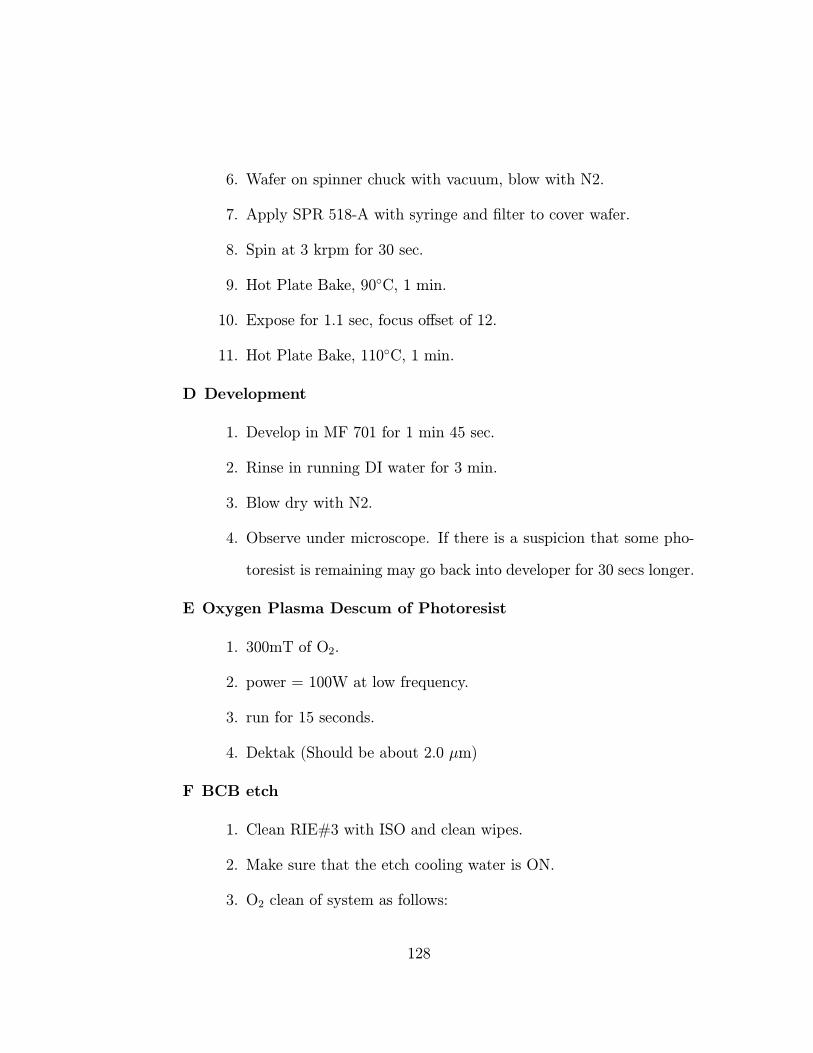
6. Wafer on spinner chuck with vacuum, blow with N2.
7. Apply SPR 518-A with syringe and filter to cover wafer.
8. Spin at 3 krpm for 30 sec.
9. Hot Plate Bake, 90C, 1 min.
10. Expose for 1.1 sec, focus offset of 12.
11. Hot Plate Bake, 110C, 1 min.
D Development
1. Develop in MF 701 for 1 min 45 sec.
2. Rinse in running DI water for 3 min.
3. Blow dry with N2.
4. Observe under microscope. If there is a suspicion that some pho-
toresist is remaining may go back into developer for 30 secs longer.
E Oxygen Plasma Descum of Photoresist
1. 300mT of O2.
2. power = 100W at low frequency.
3. run for 15 seconds.
4. Dektak (Should be about 2.0 µm)
F BCB etch
1. Clean RIE#3 with ISO and clean wipes.
2. Make sure that the etch cooling water is ON.
3. O2 clean of system as follows:
128
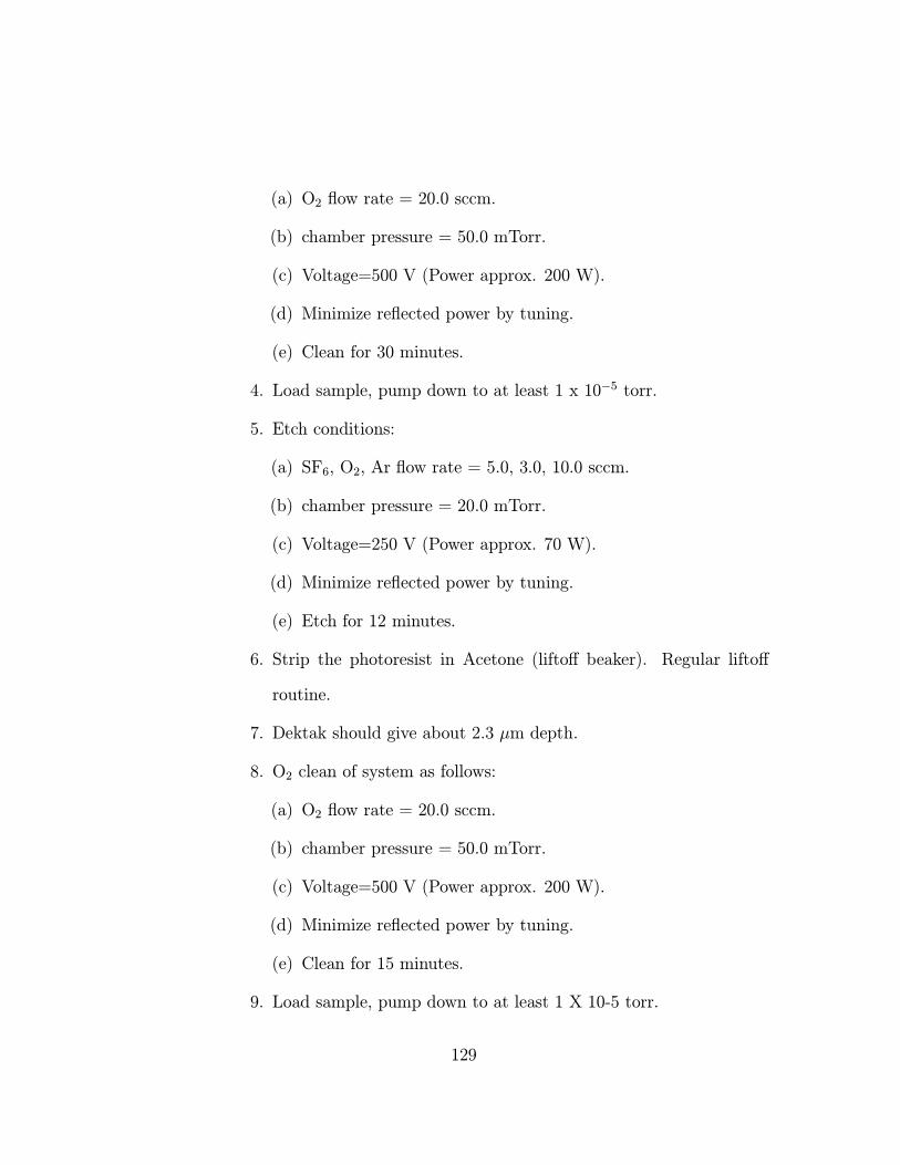
(a) O2 flow rate = 20.0 sccm.
(b) chamber pressure = 50.0 mTorr.
(c) Voltage=500 V (Power approx. 200 W).
(d) Minimize reflected power by tuning.
(e) Clean for 30 minutes.
4. Load sample, pump down to at least 1 x 10⁻⁵ torr.
5. Etch conditions:
(a) SF6, O2, Ar flow rate = 5.0, 3.0, 10.0 sccm.
(b) chamber pressure = 20.0 mTorr.
(c) Voltage=250 V (Power approx. 70 W).
(d) Minimize reflected power by tuning.
(e) Etch for 12 minutes.
6. Strip the photoresist in Acetone (liftoff beaker). Regular liftoff
routine.
7. Dektak should give about 2.3 µm depth.
8. O2 clean of system as follows:
(a) O2 flow rate = 20.0 sccm.
(b) chamber pressure = 50.0 mTorr.
(c) Voltage=500 V (Power approx. 200 W).
(d) Minimize reflected power by tuning.
(e) Clean for 15 minutes.
9. Load sample, pump down to at least 1 X 10⁻⁵ torr.
129
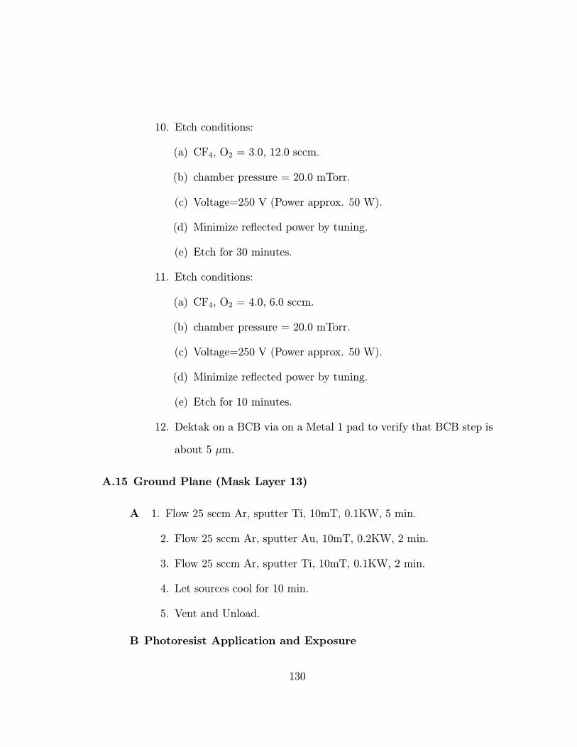
10. Etch conditions:
(a) CF4, O2 = 3.0, 12.0 sccm.
(b) chamber pressure = 20.0 mTorr.
(c) Voltage=250 V (Power approx. 50 W).
(d) Minimize reflected power by tuning.
(e) Etch for 30 minutes.
11. Etch conditions:
(a) CF4, O2 = 4.0, 6.0 sccm.
(b) chamber pressure = 20.0 mTorr.
(c) Voltage=250 V (Power approx. 50 W).
(d) Minimize reflected power by tuning.
(e) Etch for 10 minutes.
12. Dektak on a BCB via on a Metal 1 pad to verify that BCB step is
about 5 µm.
A.15 Ground Plane (Mask Layer 13)
A 1. Flow 25 sccm Ar, sputter Ti, 10mT, 0.1KW, 5 min.
2. Flow 25 sccm Ar, sputter Au, 10mT, 0.2KW, 2 min.
3. Flow 25 sccm Ar, sputter Ti, 10mT, 0.1KW, 2 min.
4. Let sources cool for 10 min.
5. Vent and Unload.
B Photoresist Application and Exposure
130
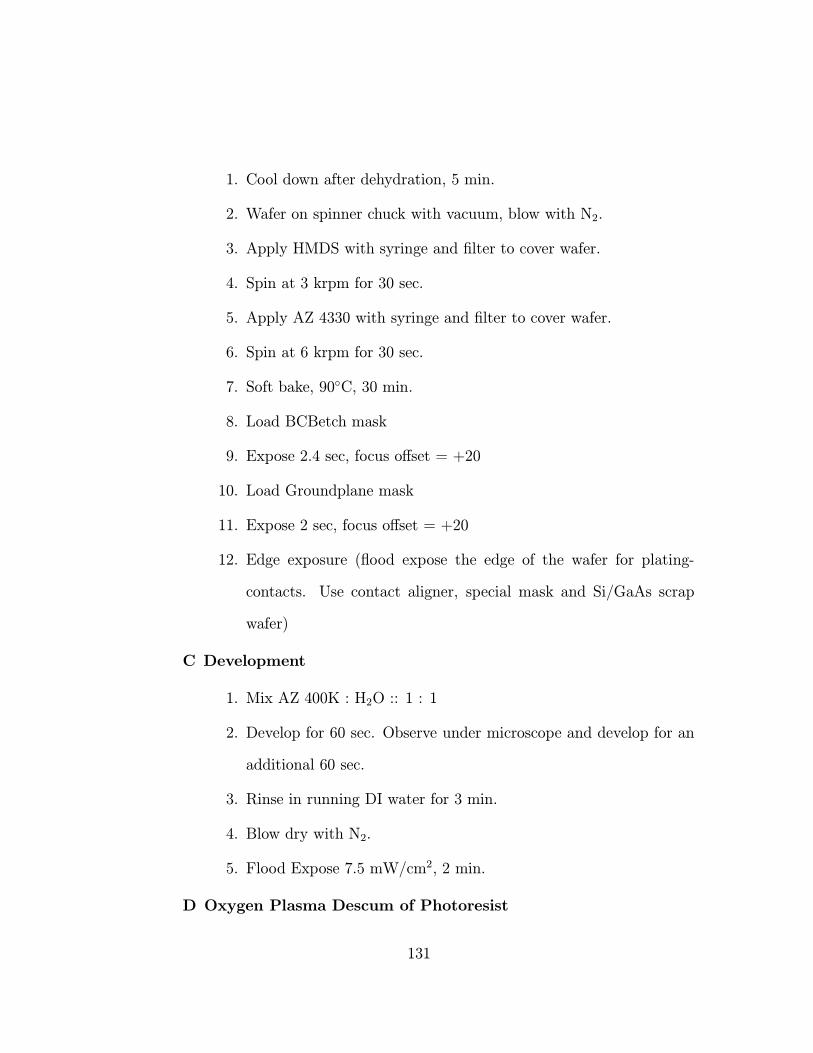
1. Cool down after dehydration, 5 min.
2. Wafer on spinner chuck with vacuum, blow with N2.
3. Apply HMDS with syringe and filter to cover wafer.
4. Spin at 3 krpm for 30 sec.
5. Apply AZ 4330 with syringe and filter to cover wafer.
6. Spin at 6 krpm for 30 sec.
7. Soft bake, 90C, 30 min.
8. Load BCBetch mask
9. Expose 2.4 sec, focus offset = +20
10. Load Groundplane mask
11. Expose 2 sec, focus offset = +20
12. Edge exposure (flood expose the edge of the wafer for plating-
contacts. Use contact aligner, special mask and Si/GaAs scrap
wafer)
C Development
1. Mix AZ 400K : H2O :: 1 : 1
2. Develop for 60 sec. Observe under microscope and develop for an
additional 60 sec.
3. Rinse in running DI water for 3 min.
4. Blow dry with N2.
5. Flood Expose 7.5 mW/cm2, 2 min.
D Oxygen Plasma Descum of Photoresist
131

1. 300mT of O2.
2. power = 100W at low frequency.
3. run for 15 seconds.
E Post Bake, 120C, 30 min.
F Ti etch
1. Mix HF:H2O :: 1:20
2. Dip in dilute HF for 20 sec
3. Rinse in running DI for 3 min
4. Blow dry with N2
G Gold Plating
1. Gold plating @ 5.4 mA, 75C, 200 rpm, for 3 hours
2. Rinse in running DI for 3 min
3. Blow dry with N2
4. Measure the profile using the Dektak
5. Observe under microscope to ensure that the small vias are plated
H AZ 4330 removal
1. Develop in AZ 400K, 90 sec
2. Rinse in running DI, 3 min
3. Blow dry with N2
4. Oxygen Plasma Descum, 300 mT, 200 W, 2 min
I Ti etch
132

1. Mix HF : H2O :: 1 : 20
2. Dip in dilute HF for 30 sec
3. Rinse in running DI, 3 min
4. Blow dry with N2
J Au etch
1. Mix etchant, KI2/I2/H2O : H2O :: 1 : 1
2. Etch for 45 seconds with stir bar at 400 rpm
3. If the gold is not etched completely, can etch for 15-20 seconds
longer
4. Rinse in running DI, 3 min
5. Blow dry with N2
K Ti etch
1. Mix HF : H2O :: 1 : 20
2. Dip in dilute HF for 30 sec
3. Rinse in running DI, 3 min
4. Blow dry with N2
133