a creative rf mems capacitive switch based on mos-type co
TRANSCRIPT

A Creative RF MEMS Capacitive Switch Based on MOS-type Co-Planar Waveguide for Space Applications
ZHAO Jiahao, YOU Zheng, CHEN Junshou
1
State Key Lab. of Precision Measurement Technology and Instruments Department of Precision Instrument and Mechanics Tsinghua University
8th ESA Round Table on Micro and Nano Technologies for Space Applications
15 - 18 October 2012 ESA/ESTEC, Noordwijk, The Netherlands

Lab. • Microsatellite and Nanosatellite Research
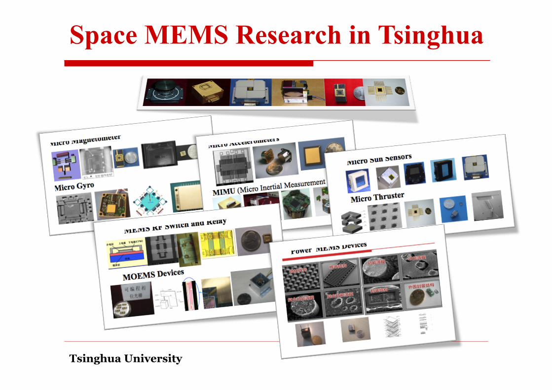
• Space MEMS Research
2
of Measurement, Control and Intelligence Micro-System

Tsinghua University
Microsatellite Research in Tsinghua University
NS-1 is smallest and highest density launched 3 Axis stable Nano-satellite in china
Tsinghua-1
(50kg,2000)
KT-PS (35kg)
KT-PS1 (35kg)
NS-1
(25kg,2004)
Successful Launched Manufactured Waiting for Launch
( 2012-2013)
NS-2
(25kg)
MEMSat
(7kg)
2000-2004 2006-2012
Tsinghua University
Space MEMS Research in Tsinghua
Outline
• Background and Space Applications
• MOS-type Co-Planar Waveguide
• RF MEMS Capacitive Switch
• Conclusion
5

Outline
• Background and Space Applications
• MOS-type Co-Planar Waveguide
• RF MEMS Capacitive Switch
• Conclusion
6

RF MEMS Switch
7
Z0 Z0C
Ls
Rs
a1
a2
b1
b2
Capacitive Switch
Resistive switch
基底
Top electrode
缓冲层
Bottom electrode
Dielectric
Buffer
Substrate
RF Signal
IN OUT
contact resistance
Control Signal
RF Signal
IN OUT
contact resistance
Control Signal Control
Contact resistance 基底 Substrate
Bottom electrode
Top electrode cantilever Dielectric Contact
Signal

RF MEMS Switch Research
8
Main direction Major approaching Current development
Low driving voltage
Low-K design, low residual stress design, reduce the distance, increase the area
H-type beam, Elastic bending beam, Slotted beam
7~20V
Low insertion loss &. High isolation
Low losses CPW
CPW with suspending structure, Special substrate, Low loss conductor
<0.20dB@35GHz
High power Varied driving types, Varied driving structures
Comb driving, Thermal driving, Disc structure, Sandwich structure
>10W
High reliability Thermal stability, Radiation stability, Impact load stability
Reliability model, key factors, Reliability design
1011
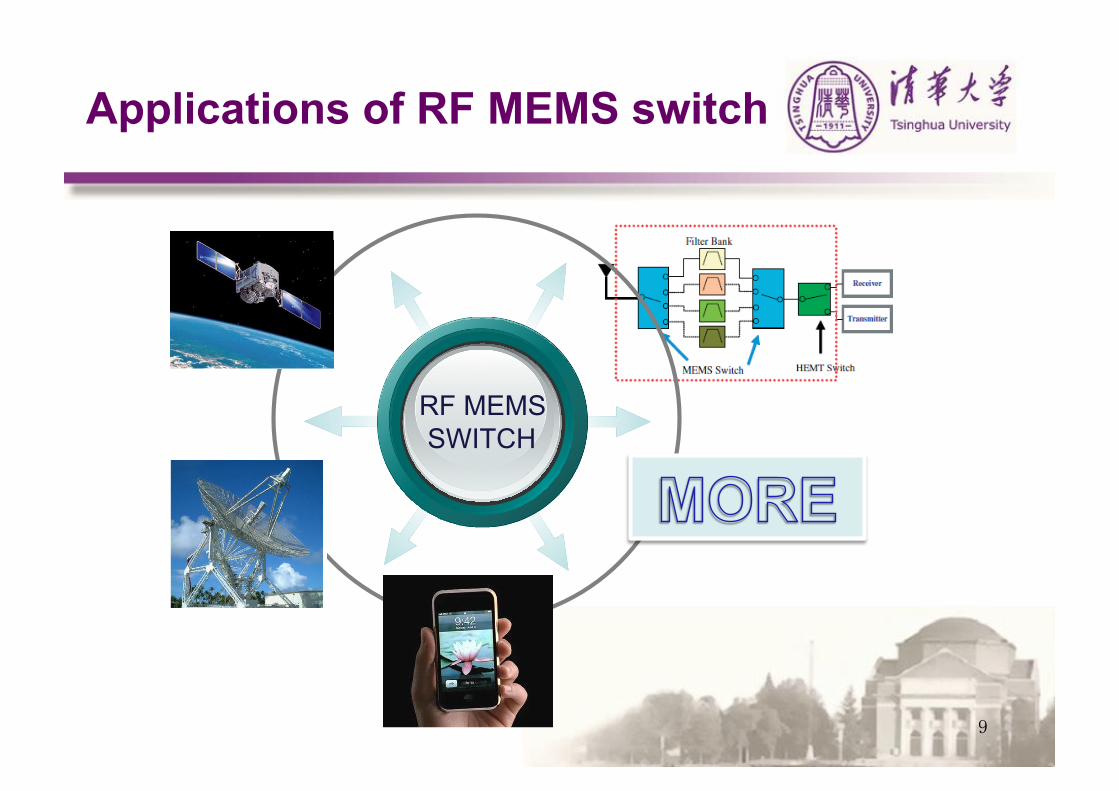
Applications of RF MEMS switch
9
RF MEMS SWITCH
Outline
• Background and Space Applications
• MOS-type Co-Planar Waveguide
• RF MEMS Capacitive Switch
• Conclusion
10

Co-Planar Waveguides, CPW
• Key Component of RF MEMS switch • Important related to the losses of switch device • CPW with low losses High performance device
• Advantages of CPW • No aperture inside the substrate - compared with micro-strip transmission line • All the wires located on the same layer- convenience for integration with MMIC
11
Earth
Substrate
Signal

tan8.68 rsub
q g
qε θα π
ε λ= ⋅
( ) ( )2 25 3 2
, 33
,
1 22
2 '( ) ( )eff f r r
radeff f r
s wf
c K k K kε ε επ
αε ε
⎛ ⎞− +⎛ ⎞ ⎜ ⎟= ⎜ ⎟ ⎜ ⎟⎝ ⎠⎝ ⎠
40 2
1.25 1.25 41 ln4.88 10 1
1.25 42 1 lncond s q
t sP s s tR Zw w s t s
w w t
ππ πα ε
π ππ
−+ +
⎛ ⎞= × + ×⎜ ⎟⎝ ⎠ ⎛ ⎞⎛ ⎞+ − +⎜ ⎟⎜ ⎟
⎝ ⎠⎝ ⎠
Losses of CPW
• Conductor Loss
• Substrate Loss
• Radiation Loss
12
Earth
Substrate
Signal
[1] Liao C L, Tu Y M, Ke J Y, et al. Transient propagation in lossy coplanar waveguides. IEEE Transactions on Microwave Theory and Techniques, 1996,44(12 /2):2605-2611. [2] K. C. Gupta R G A L. Microstrip Lines and Slotlines. New York: Artech House, 1979. [3] Heinrich W. Quasi-TEM description of MMIC coplanar lines including conductor-loss effects. IEEE Transactions on Microwave Theory and Techniques, 1993,41(1):45-52. [4] Frankel M Y, Gupta S, Valdmanis J A, et al. Terahertz attenuation and dispersion characteristics of coplanar transmission lines. IEEE Transactions on Microwave Theory and Techniques, 1991,39(6):910-916
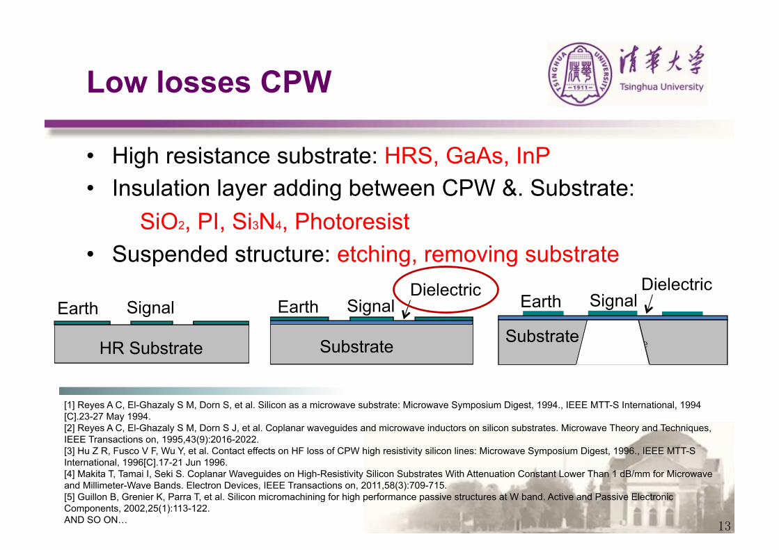
Low losses CPW
• High resistance substrate: HRS, GaAs, InP • Insulation layer adding between CPW &. Substrate:
SiO2, PI, Si3N4, Photoresist • Suspended structure: etching, removing substrate
13
[1] Reyes A C, El-Ghazaly S M, Dorn S, et al. Silicon as a microwave substrate: Microwave Symposium Digest, 1994., IEEE MTT-S International, 1994 [C].23-27 May 1994. [2] Reyes A C, El-Ghazaly S M, Dorn S J, et al. Coplanar waveguides and microwave inductors on silicon substrates. Microwave Theory and Techniques, IEEE Transactions on, 1995,43(9):2016-2022. [3] Hu Z R, Fusco V F, Wu Y, et al. Contact effects on HF loss of CPW high resistivity silicon lines: Microwave Symposium Digest, 1996., IEEE MTT-S International, 1996[C].17-21 Jun 1996. [4] Makita T, Tamai I, Seki S. Coplanar Waveguides on High-Resistivity Silicon Substrates With Attenuation Constant Lower Than 1 dB/mm for Microwave and Millimeter-Wave Bands. Electron Devices, IEEE Transactions on, 2011,58(3):709-715. [5] Guillon B, Grenier K, Parra T, et al. Silicon micromachining for high performance passive structures at W band. Active and Passive Electronic Components, 2002,25(1):113-122. AND SO ON…
Earth
HR Substrate
Signal Earth
Substrate
Signal Dielectric
Substrate
Earth
Substrate
Signal Dielectric

Dielectric layer
• CPW with Insulation layer – Help to reduce DC loss – Bring Dielectric loss �
• Dielectric Layer – Interface effect – Process quality – Crystal lattice mismatching with substrate
14
[1] Pfeifer T, Heiliger H M, Stein Von Kamienski E, et al. Charge accumulation effects and microwave absorption of coplanar waveguides fabricated on high-resistivity Si with SiO2 insulation layer. Applied Physics Letters, 1995,67(18):2624. [2] Reyes A C, El-Ghazaly S M, Dorn S J, et al. Coplanar waveguides and microwave inductors on silicon substrates. Microwave Theory and Techniques, IEEE Transactions on, 1995,43(9):2016-2022.
Substrate HRS Insulation layer ↑
Non-insulator ↓
HR Silicon
Au
SiO2
Work function difference
Interface state
Carrier transporting
Low resistance layer
CPW Losses↑
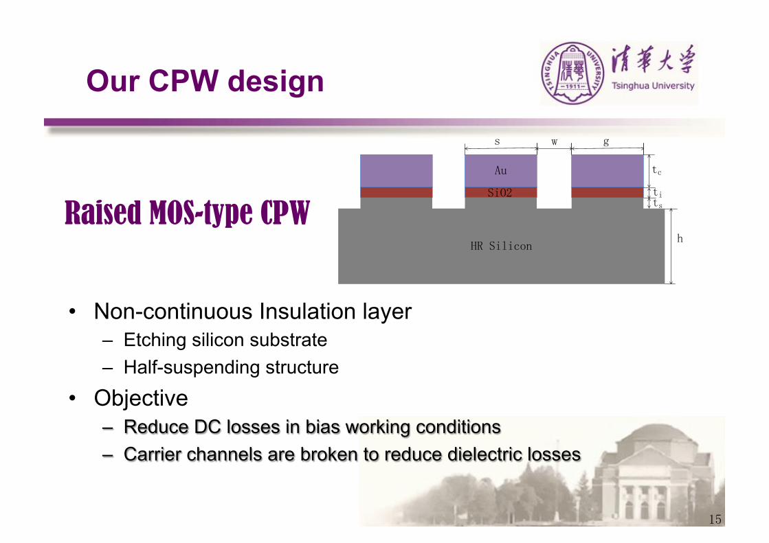
Our CPW design
15
HR Silicon
Au
SiO2
tc
tits
h
s w g
• Non-continuous Insulation layer – Etching silicon substrate – Half-suspending structure �
• Objective – Reduce DC losses in bias working conditions – Carrier channels are broken to reduce dielectric losses
Raised MOS-type CPW

Outline
• Background and Space Applications
• MOS-type Co-Planar Waveguide
• RF MEMS Capacitive Switch
• Conclusion
16
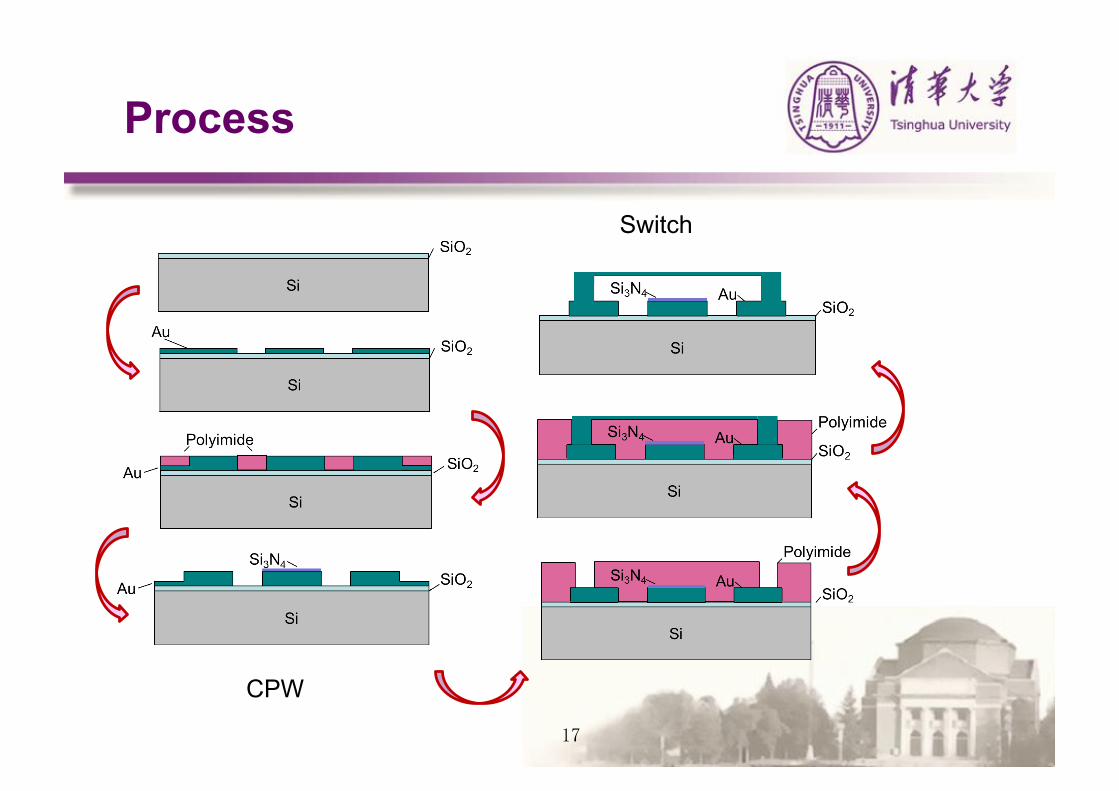
Process
17
CPW
Switch
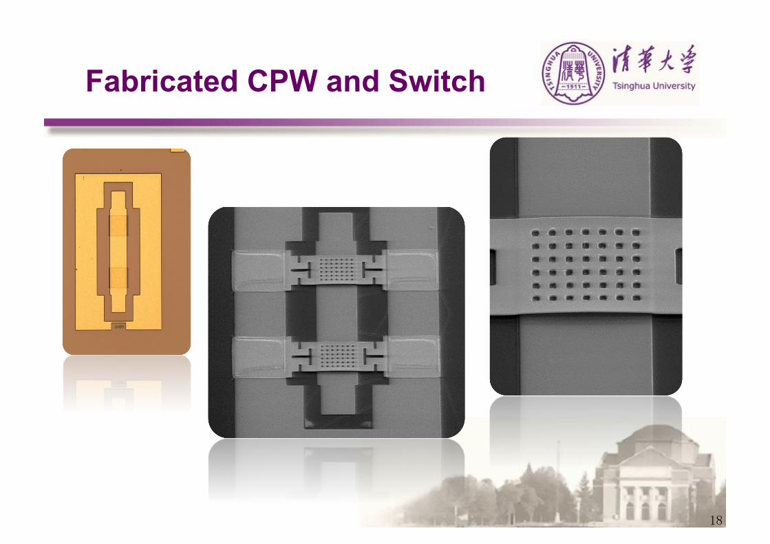
Fabricated CPW and Switch
18

120
90
150
500
20
700
HR Silicon
Au
SiO2
tc
tits
h
s w g
Return loss
19 0 10 20 30 40
-50
-40
-30
-20
-10
0
Freq./GHz
Ret
urn
loss/d
B
0V +20 +40V
0 10 20 30 40
-60
-50
-40
-30
-20
-10
0
0V -20 -40V
Ret
urn
loss/d
B
Freq./GHz

Insertion [email protected]
20
-40 -30 -20 -10 0 10 20 30 40
-0.25
-0.2
-0.15
-0.1
-0.05
0
Bias/V)
S21(
dB)

Energy loss
21
120
90
150
500
20
700
120
90
150
500
50
700
-40 -30 -20 -10 0 10 20 30 40
-0.25
-0.2
-0.15
-0.1
-0.05
0
Bias/V
Ene
rgy
Los
s /dB
To our knowledge, this is the best result in the publications of silicon substrate based CPW at Ka-band.

Driving Voltage of the Switch
22
CV curve: 32V
5 10 15 20 25 30 35 40 0
0.2
0.4
0.6
0.8
1
1.2
1.4 x 10
-12
Applied voltage/V
C/F

Insertion loss
23
-0.14dB@35GHz, -0.28dB@0~37GHz, -0.36dB@0~40GHz
0
0 5 10 15 20 25 30 35 40 -0.4
-0.35
-0.3
-0.25
-0.2
-0.15
-0.1
-0.05
Freq.(GHz)
Inse
rtion
loss(d
B)
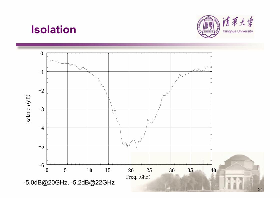
Isolation
24
-5.0dB@20GHz, -5.2dB@22GHz
0 5 10 15 20 25 30 35 40 -6
-5
-4
-3
-2
-1
0
isol
atio
n(dB
)
Freq.(GHz)

Conclusion
• We discussed the raised MOS-type CPW with low losses and
RF MEMS capacitive switch for aerospace applications.
• The fabricated CPW lines achieve an Energy loss
lower than -0.010 dB/mm at 35GHz
• The RF MEMS switches achieves an insertion losses
lower than -0.14dB at 35GHz
25

Thank You for Attention!
26