a custom layout of a 8 bit risc...
TRANSCRIPT
A Custom Layout of a
8 bit RISC Microcontroller
By
Kalyan Parajuli
Bachelor of Engineering
Kathmandu University
Dhulikhel, Nepal
2000
Submitted to the Faculty of the Graduate College of the
Oklahoma State University In partial fulfillment of
the requirements for the Degree of
MASTER OF SCIENCE MAY 2005
ii
A Custom Layout of a
8 bit RISC Microcontroller
Thesis Approved:
Thesis Advisor
Dean of Graduate College
iii
ABSTRACT
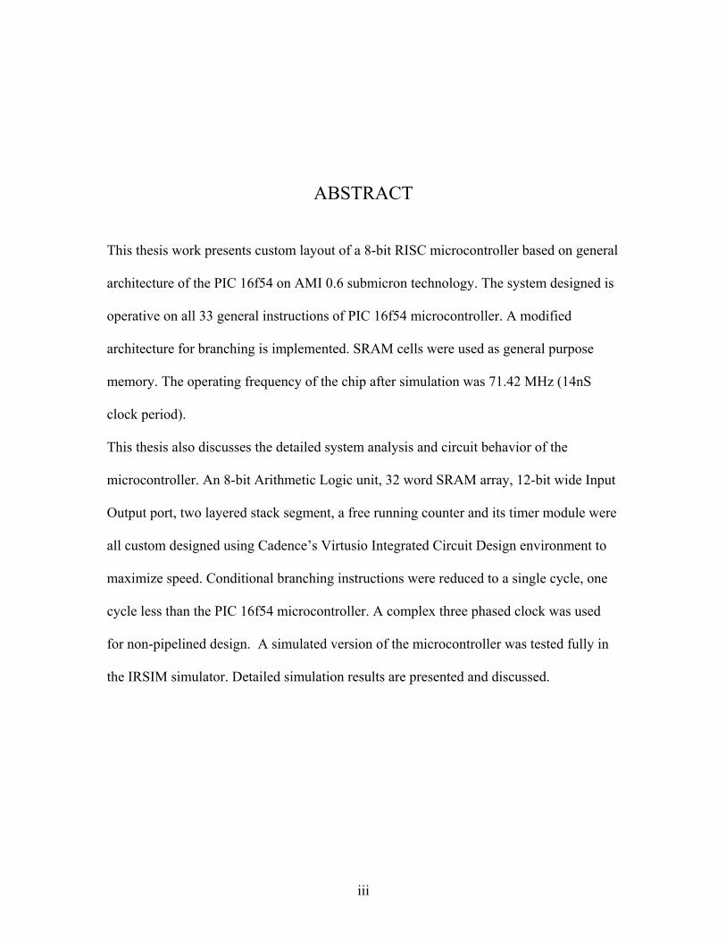
This thesis work presents custom layout of a 8-bit RISC microcontroller based on general
architecture of the PIC 16f54 on AMI 0.6 submicron technology. The system designed is
operative on all 33 general instructions of PIC 16f54 microcontroller. A modified
architecture for branching is implemented. SRAM cells were used as general purpose
memory. The operating frequency of the chip after simulation was 71.42 MHz (14nS
clock period).
This thesis also discusses the detailed system analysis and circuit behavior of the
microcontroller. An 8-bit Arithmetic Logic unit, 32 word SRAM array, 12-bit wide Input
Output port, two layered stack segment, a free running counter and its timer module were
all custom designed using Cadence’s Virtusio Integrated Circuit Design environment to
maximize speed. Conditional branching instructions were reduced to a single cycle, one
cycle less than the PIC 16f54 microcontroller. A complex three phased clock was used
for non-pipelined design. A simulated version of the microcontroller was tested fully in
the IRSIM simulator. Detailed simulation results are presented and discussed.

iv
ACKNOWLEDGEMENTS
I would like to thank my advisor, Dr. Louis G. Johnson, for his continuous guidance,
encouragement and support during the work on this thesis. I also wish to thank Dr. Daniel
Grischkowsky and Dr. R. G. Ramakumar for reviewing my thesis and for their valuable
comments and suggestions concerning this work as members of my advisory committee.
Additional thanks go to my friends for being available for helpful discussions.
My sincere appreciation goes to my brother, sisters and sister-in-law for their assistance
and knowledge and also to little Jhyankur for many good words in hard time.
I am deeply grateful to my lovely wife Sarika, for accompanying me through my studies,
her endurance and support.
Finally, my parents deserve most of my gratitude for everything they have done a life
long for me.
v
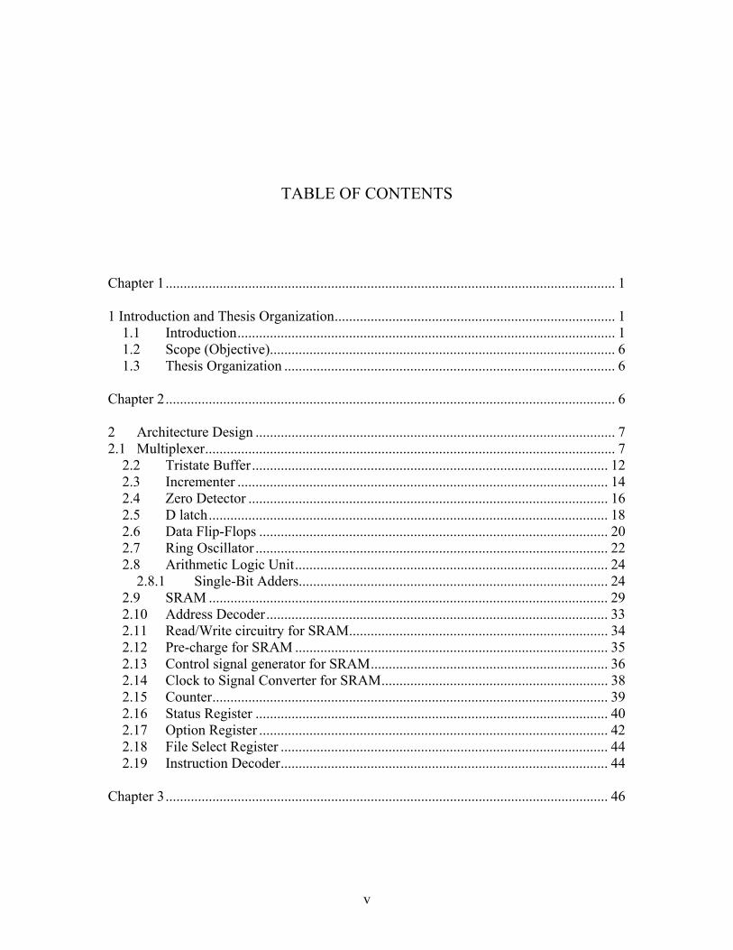
TABLE OF CONTENTS
Chapter 1............................................................................................................................. 1 1 Introduction and Thesis Organization.............................................................................. 1
1.1 Introduction......................................................................................................... 1 1.2 Scope (Objective)................................................................................................ 6 1.3 Thesis Organization ............................................................................................ 6
Chapter 2............................................................................................................................. 6 2 Architecture Design .................................................................................................... 7 2.1 Multiplexer.................................................................................................................. 7
2.2 Tristate Buffer................................................................................................... 12 2.3 Incrementer ....................................................................................................... 14 2.4 Zero Detector .................................................................................................... 16 2.5 D latch............................................................................................................... 18 2.6 Data Flip-Flops ................................................................................................. 20 2.7 Ring Oscillator .................................................................................................. 22 2.8 Arithmetic Logic Unit....................................................................................... 24
2.8.1 Single-Bit Adders...................................................................................... 24 2.9 SRAM ............................................................................................................... 29 2.10 Address Decoder............................................................................................... 33 2.11 Read/Write circuitry for SRAM........................................................................ 34 2.12 Pre-charge for SRAM ....................................................................................... 35 2.13 Control signal generator for SRAM.................................................................. 36 2.14 Clock to Signal Converter for SRAM............................................................... 38 2.15 Counter.............................................................................................................. 39 2.16 Status Register .................................................................................................. 40 2.17 Option Register ................................................................................................. 42 2.18 File Select Register ........................................................................................... 44 2.19 Instruction Decoder........................................................................................... 44
Chapter 3........................................................................................................................... 46

vi
3 Modular Design ........................................................................................................ 46 3.1 SRAM array ...................................................................................................... 46 3.2 Stack Segment................................................................................................... 48 3.3 Accumulator...................................................................................................... 50 3.4 Program Counter............................................................................................... 51 3.5 Bit Test.............................................................................................................. 52 3.6 Rotate and Swap ............................................................................................... 52 3.7 Input Output Port .............................................................................................. 52 3.8 Timer 0 Module ................................................................................................ 54
3.8.1 Timer0 Register ........................................................................................ 54 3.8.2 Prescalar.................................................................................................... 54 3.8.3 Watch Dog Timer ..................................................................................... 55
3.9 Instruction Decoder........................................................................................... 56 3.10 Data path , Signal Routing and Controlling...................................................... 62 3.11 Status Register .................................................................................................. 67
Chapter 4........................................................................................................................... 68 4 Instruction Execution ................................................................................................ 68
4.1 Byte Oriented Instructions ................................................................................ 68 4.1.1 ADDWF.................................................................................................... 68 4.1.2 ANDWF.................................................................................................... 69 4.1.3 CLRF......................................................................................................... 70 4.1.4 CLRW....................................................................................................... 71 4.1.5 COMF ....................................................................................................... 72 4.1.6 DECF ........................................................................................................ 72 4.1.7 DECFSZ.................................................................................................... 73 4.1.8 INCF ......................................................................................................... 74 4.1.9 INCFSZ..................................................................................................... 75 4.1.10 IORWF...................................................................................................... 76 4.1.11 MOVF....................................................................................................... 77 4.1.12 MOVWF ................................................................................................... 78 4.1.13 NOP........................................................................................................... 79 4.1.14 RLF ........................................................................................................... 80 4.1.15 RRF........................................................................................................... 81 4.1.16 SUBWF..................................................................................................... 82 4.1.17 SWAPF ..................................................................................................... 83 4.1.18 XORWF .................................................................................................... 84
4.2 Bit Oriented Instructions................................................................................... 85
vii
4.2.1 BCF........................................................................................................... 85 4.2.2 BSF ........................................................................................................... 86 4.2.3 BTFSC ...................................................................................................... 87 4.2.4 BTFSS....................................................................................................... 88
4.3 Literal and Control Instructions ........................................................................ 89 4.3.1 ANDLW.................................................................................................... 89 4.3.2 IORLW ..................................................................................................... 90 4.3.3 MOVLW................................................................................................... 90 4.3.4 XORLW.................................................................................................... 91 4.3.5 CALL ........................................................................................................ 92 4.3.6 GOTO ....................................................................................................... 93 4.3.7 TRIS.......................................................................................................... 94
5 Conclusion and Future Work .................................................................................... 95
5.1 Future Work ...................................................................................................... 97 6 References................................................................................................................. 98 7 Bibliography ........................................................................................................... 100 Appendixes ..................................................................................................................... 101
A. Test benches........................................................................................................... 101 A.1 Test bench for 8 bit ALU ................................................................................. 101 A.2 Test bench for 32 word memory array............................................................. 108
viii
LIST OF TABLES
Table 2-1 Comparison of Multiplexer delays and layout area.......................................... 12
Table 2-2 D latch functional table .................................................................................... 18
Table .2-3 Binary Addition .............................................................................................. 25
Table 2-4 Prescaling Rate ................................................................................................ 43
ix
LIST OF FIGURES
Figure 1-1 General Structure of a Harvard Architecture .................................................... 4
Figure 1-2 Generalized block diagram of a 8 bit RISC microcontroller ............................ 5
Figure 2-1 2 to 1 multiplexer .............................................................................................. 7
Figure 2-2 4 to 1 multiplexer ............................................................................................. 9
Figure 2-3 8 to 1 multiplexer .............................................................................................. 9
Figure 2-4 Layout of a 2 to 1 multiplexer......................................................................... 10
Figure 2-5 Testing 2 to 1 multiplexer ............................................................................... 10
Figure 2-6 8 to 1 multiplexer ............................................................................................ 11
Figure 2-7 8-bit 2 to 1 multiplexer.................................................................................... 11
Figure 2-8 Schematic of a Tristate Buffer ........................................................................ 12
Figure 2-9 Layout of a tristate buffer................................................................................ 13
Figure 2-10 Timing diagram of a tristate buffer ............................................................... 14
Figure 2-11 Structure of a 2 bit Incrementer .................................................................... 15
Figure 2-12 State Diagram of a 8 bit incrementer ............................................................ 15
Figure 2-13 Output of 9-bit incrementer........................................................................... 16
Figure 2-14 Schematics of a zero detector........................................................................ 16
Figure 2-15 Layout of a zero detector............................................................................... 17
Figure 2-16 Timing diagram of a zero detector ................................................................ 17
x
Figure 2-17 Basic Latch.................................................................................................... 18
Figure 2-18 Layout of a D latch........................................................................................ 19
Figure 2-19 Output of a D latch........................................................................................ 20
Figure 2-20 A positive edge triggered D flip flop ............................................................ 20
Figure 2-21 State diagram of a positive edge triggered D-type Flip-flop......................... 21
Figure 2-22 Layout of 8-bit D type flip-flop .................................................................... 21
Figure 2-23 Simulation of 8-bit D type flip-flop .............................................................. 22
Figure 2-24 Ring Oscillator .............................................................................................. 22
Figure 2-25 Waveform of three nodes of a ring oscillator Vx,Vy, and Vz........................ 23
Figure 2-28 Block Diagram of a full adder....................................................................... 24
Figure 3.18 Carry propagation signal blocked for XOR operation .................................. 26
Figure 3.19 A input pin for ALU...................................................................................... 26
Figure 3.20 ALU operations multiplexed ......................................................................... 27
Figure 2-29 Layout of 1-bit ALU cell............................................................................... 28
Figure 2-30 Output of 4 operations of ALU ..................................................................... 29
Figure 2-31 A 6 transistor Static RAM cell. ..................................................................... 30
Figure 2-32 A 6-Transistor Static RAM cell with write driver. ....................................... 30
Figure 2-33 SRAM cell layout.......................................................................................... 32
Figure 2-34 SRAM test result ........................................................................................... 32
Figure 2-35 Schematic Diagram of a address decoder ..................................................... 33

xi
Figure 2-36 Layout of single bit address decoder............................................................. 34
Figure 2-37 read/write circuitry for SRAM...................................................................... 35
Figure 2-38 Layout of read/write circuitry for SRAM ..................................................... 35
Figure 2-39 Schematic of signal generator ....................................................................... 36
Figure 2-40 Layout of signal generator ............................................................................ 37
Figure 2-41 Timing Diagram of signal generator ............................................................. 37
Figure 2-42 SRAM internal clock generation................................................................... 38
Figure 2-43 A single bit counter ....................................................................................... 39
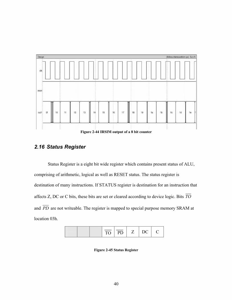
Figure 2-44 IRSIM output of a 8 bit counter .................................................................... 40
Figure 2-45 Status Register............................................................................................... 40
Figure 2-46 Bit allocation in a Option register ................................................................. 42
Figure 2-47 Addressing memory with FSR..................................................................... 44
Figure 3-1 Block Diagram of a SRAM array.................................................................... 46
Figure 3-2 SRAM array .................................................................................................... 47
Figure 3-3 Position of blocks with reference to Figure 3-2 .............................................. 47
Figure 3-4 SRAM array testing......................................................................................... 48
Figure 3-5 Stack Architecture........................................................................................... 49
Figure 3-6 Read Write Timing Diagram of Stack ........................................................... 50
Figure 3-7 Execution of GOTO and CALL instruction.................................................... 51
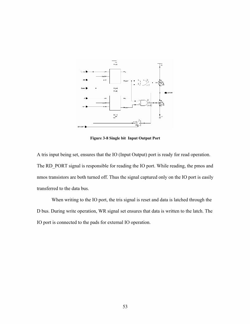
Figure 3-8 Single bit Input Output Port ........................................................................... 53

xii
Figure 3-9 Timer0 module ................................................................................................ 55
Figure 3-10 Generation of Positive edge or negative edge clock for Timer0 module...... 55
Figure 3-11 Generation of ramwr signal by MOVF instruction. ..................................... 57
Figure 3-12 Skipping the count of present instruction from zero result ........................... 57
Figure 3-13 Swapping by execution of a SWAPF instruction.......................................... 58
Figure 3-14 Data Path and Control ................................................................................... 62
Figure 3-15 asel and bsel controlling datapath to ALU.................................................... 63
Figure 3-16 A COMF operation ....................................................................................... 64
Figure 3-17 Bit Test Operation ......................................................................................... 64
Figure 3-18 Execution of RRF and RLF instruction with ALU bypassed ....................... 65
Figure 3-19 SWAPF instruction with swap_en pin .......................................................... 66
Figure 3-20 WB pin selecting SRAM_IN operation ........................................................ 66
Figure 4-1 ADDWF operation .......................................................................................... 69
Figure 4-2 ANDWF operation .......................................................................................... 70
Figure 4-3 CLRF operation............................................................................................... 71
Figure 4-4 CLRW operation ............................................................................................. 72
Figure 4-5 A COMF operation ......................................................................................... 72
Figure 4-6 A DECF operation........................................................................................... 73
Figure 4-7 DECFSZ operation.......................................................................................... 74
Figure 4-8 A INCF operation............................................................................................ 75

xiii
Figure 4-9 A INCFSZ operation ....................................................................................... 76
Figure 4-10 IORWF instruction........................................................................................ 77
Figure 4-11 A MOVF operation ....................................................................................... 78
Figure 4-12 A NOP operation........................................................................................... 80
Figure 4-13 A RLF operation ........................................................................................... 81
Figure 4-14 A RRF operation ........................................................................................... 82
Figure 4-15 A SUBWF instruction................................................................................... 83
Figure 4-16 A SWAPF instruction ................................................................................... 84
Figure 4-17 A XORWF operation .................................................................................... 85
Figure 4-18 A BCF instruction ......................................................................................... 86
Figure 4-19 A BSF operation............................................................................................ 87
Figure 4-20 A BTFSC operation....................................................................................... 88
Figure 4-21 A BTFSS operation....................................................................................... 88
Figure 4-22 A ANDLW instruction.................................................................................. 89
Figure 4-23 A IORLW instruction................................................................................... 90
Figure 4-24 A MOLW instruction execution.................................................................... 91
Figure 4-25 A XORLW operation .................................................................................... 92
Figure 4-26 A CALL instruction execution...................................................................... 93
Figure 4-27 A GOTO operation........................................................................................ 93
Figure 4-28 A TRIS operation .......................................................................................... 94
xiv
NOMENCLATURE
IO Input Output
RAM Random Access Memory
SRAM Static Random Access Memory
DFF Data Flip Flop
ALU Arithmetic Logical Unit
1 Bit is set
0 Bit is cleared
u Unimplemented Bit
XOR Exclusive OR
AND Logical AND operation
IOR Inclusive OR operation
WDT Watch Dog Timer
PSA Prescalar Assignment Bit
M1, metal1 Metal 1
M2, metal2 Metal 2
M3, metal3 Metal3
Poly Poly silicon
XXX h hexadecimal
xv
LSb Lowest Significant Bit
MSb Most Significant Bit
x(W)*y(H) x micrometers in width by y micrometers in height
1
Chapter 1
1 Introduction and Thesis Organization
1.1 Introduction
Contents of many different circuits put on a single chip, makes an integrated circuit. With
introduction of the integrated circuit, all the peripheral devices and microprocessor was
put on a single device. This led to development of a microcontroller. A microcontroller
differs from microprocessor in many ways. Most important aspect is with the
functionality. In order for a microprocessor to be functional, other components as
memory or components for receiving and sending data must be added to it. In short
microprocessor is the very heart of the computer. On the other hand, microcontroller is
designed to be all of that in one. No other external components are needed for its
application as all necessary components are built to it. Thus we save the time and space
needed to construct devices.
Memory location in a microcontroller simply means that we are getting some valid data
with certain input as address locations. Arithmetic Logic Unit, a.k.a. ALU, takes data
from certain memory locations or Input Output port and then perform addition,
subtraction, AND, OR, XOR,NOT or combination of these. Bus on microcontroller
2
simply represents group of 8 or more wires responsible for transferring data and address.
In addition to these there are some pins that can be interfaced to the outside world. These
locations are called as ports. Depending upon the control signal input to the port, it can
operate as input or output terminal. In order to utilize its full functionality, we need a
timer block, whose information can be used for time elapsed, duration and control
signals. Also a separate unit, Watch Dog Timer is introduced in microcontroller. This unit
when activated will reset the program sequence after a certain time. This function is very
important in many times when some external interference take place and the program
functions incorrectly.
In our system Reduced Instruction Set Computer (RISC) architecture is used. These are
specific type of microprocessors which recognizes limited number of instructions. Until
the mid-1980s, the tendency among computer manufacturers was to build increasingly
complex CPUs that had ever-larger sets of instructions. At that time, however, a number
of computer manufacturers decided to reverse this trend by building CPUs capable of
executing only a very limited set of instructions. One advantage of reduced instruction set
computers is, they execute their instructions very fast because the instructions are so
simple. Another, perhaps more important advantage, is that RISC architecture requires
fewer transistors, which makes them cheaper to design and produce.
Back end level design of an Integrated Circuit is basically done in two different ways,
Application-Specific Integrated Circuit (ASIC) style flow and full custom layout. A

3
custom layout means polygon-level layout done for the integrated circuit. A lot of people
use this method to increase speed reduce area.
This report presents design of 8 bit RISC microcontroller. This microcontroller is
capable of performing function of 33 instruction words. The basic input signal is given to
the instruction memory. The stored code in instruction memory will be will be decoded
through several stages including arithmetic logic unit, (ALU) and then written to
input/output port devices or to the memory. Arithmetic and logical operations as add,
subtract, exclusive or, inclusive or, complement it. Other options of setting or resetting
certain bit position can be done. It has two output ports: one is 8 bit port and the other as
4 bit port. These ports can be individually programmed to be input or output ports. This
design is done on AMI 0.6 technology, which has faster access time because of smaller
size.This design is replica of PIC 1654 microcontroller from Microchip (designed on
AMI 0.6 micron technology). It employs RISC architecture with 33 single words per
single cycle instructions. All the instructions are single cycled except branching
instructions which comprises of two cycles. The instructions are 12 bit wide. These
instructions are stored in program memory and are addressed by program counter (PC).
Additional features including power on reset, device reset timers are plus point to
the layout. This microcontroller has a self running oscillator, as well as can be
programmed and scaled down to factor of 256 or 128 depending upon mode through
software control. Also, low power consumption of the design and reduced mask layout
4
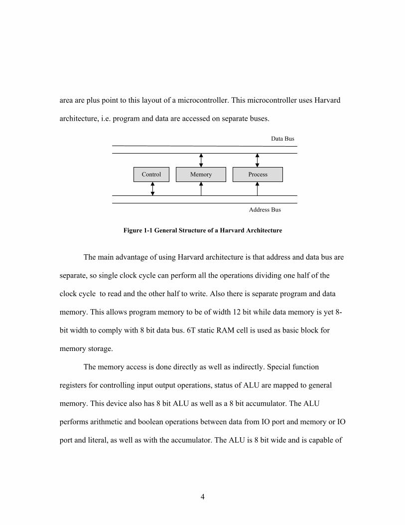
area are plus point to this layout of a microcontroller. This microcontroller uses Harvard
architecture, i.e. program and data are accessed on separate buses.
Figure 1-1 General Structure of a Harvard Architecture
The main advantage of using Harvard architecture is that address and data bus are
separate, so single clock cycle can perform all the operations dividing one half of the
clock cycle to read and the other half to write. Also there is separate program and data
memory. This allows program memory to be of width 12 bit while data memory is yet 8-
bit width to comply with 8 bit data bus. 6T static RAM cell is used as basic block for
memory storage.
The memory access is done directly as well as indirectly. Special function
registers for controlling input output operations, status of ALU are mapped to general
memory. This device also has 8 bit ALU as well as a 8 bit accumulator. The ALU
performs arithmetic and boolean operations between data from IO port and memory or IO
port and literal, as well as with the accumulator. The ALU is 8 bit wide and is capable of
Control Memory Process
Data Bus
Address Bus
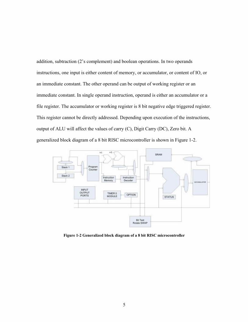
5
addition, subtraction (2’s complement) and boolean operations. In two operands
instructions, one input is either content of memory, or accumulator, or content of IO, or
an immediate constant. The other operand can be output of working register or an
immediate constant. In single operand instruction, operand is either an accumulator or a
file register. The accumulator or working register is 8 bit negative edge triggered register.
This register cannot be directly addressed. Depending upon execution of the instructions,
output of ALU will affect the values of carry (C), Digit Carry (DC), Zero bit. A
generalized block diagram of a 8 bit RISC microcontroller is shown in Figure 1-2.
Figure 1-2 Generalized block diagram of a 8 bit RISC microcontroller
6
1.2 Scope (Objective) This report focuses on a custom design aspect of an 8-bit microcontroller. This project
was designed with a scope of analyzing difference in performance using AMI 0.6
technology, and verifying the differences on different aspects of architecture, which were
modified later. This report also focuses in different components used in a microcontroller
and their testing results.
1.3 Thesis Organization
The whole document is divided five different subsections. Chapter 2 discusses design
approaches used in the design. Chapter 3 discusses on design aspects large circuitry and
their test results. Chapter 4 explains operation of all 33 instructions in a PIC instruction
set. Chapter 5 presents conclusion and future work that can be done. Chapter 6 presents
test vectors used for testing few sub-modules.
7
Chapter 2
2 Architecture Design
Architecture Design was done in schematics and then in layout. Simulations of lower
level cells were done on schematic and tested mostly using spectreS. Later using Virtuoso
layout editor from Cadence, detailed layout was drawn. This section describes detailed
design and its test results. Before testing the layout, layout of all combinational logics
was drawn and symbol view of each blocks were created. These symbol views were used
as input modules for Schematics. The output was observed, analyzed and then drawn on
layout editor for higher level designs.
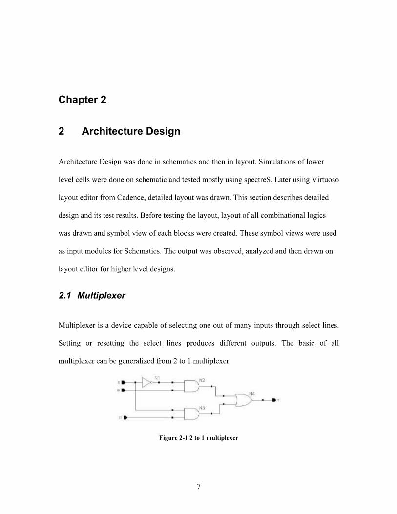
2.1 Multiplexer
Multiplexer is a device capable of selecting one out of many inputs through select lines.
Setting or resetting the select lines produces different outputs. The basic of all
multiplexer can be generalized from 2 to 1 multiplexer.
Figure 2-1 2 to 1 multiplexer
8
The output in a two to one multiplexer depends upon value of select pin. Depending upon
select pin (set or reset), output will switch accordingly. The operation of a two to one
multiplexer can be explained by the following logic equation:
y=SI1 + S I0
where y= output of multiplexer,
S=control input of multiplexer
I0, I1 = two different inputs to a multiplexer
The above equation can be simplified to ( S + A )(S+B)
The schematic of a 2 to 1 multiplexer was drawn to a minimum sized transistors. Here,
select line s denotes which of the inputs among I0 and I1 will be passed to the output.
N3 is logic high when S and I1 both are high. At the same time, output of N2 depends
upon inverted S, (through N1) and I0. Thus the output y will be high if either output of N2
or N3 is logic high. Similarly, output of N3 is low irrespective of input I1 . Thus output y
will follow input pin I0. Similarly if input S =1, then N2 will always have output 0,
irrespective of input I0. Thus output of gate N4, i.e., y will always follow input I1.
4 to 1 multiplexers, 8 to 1 multiplexers were designed with 2 to 1 multiplexer as lower
level cell. Figure 2.2 and Figure 2.3 shows symbolic connections of 4 to 1 and 8 to 1
multiplexers.
9
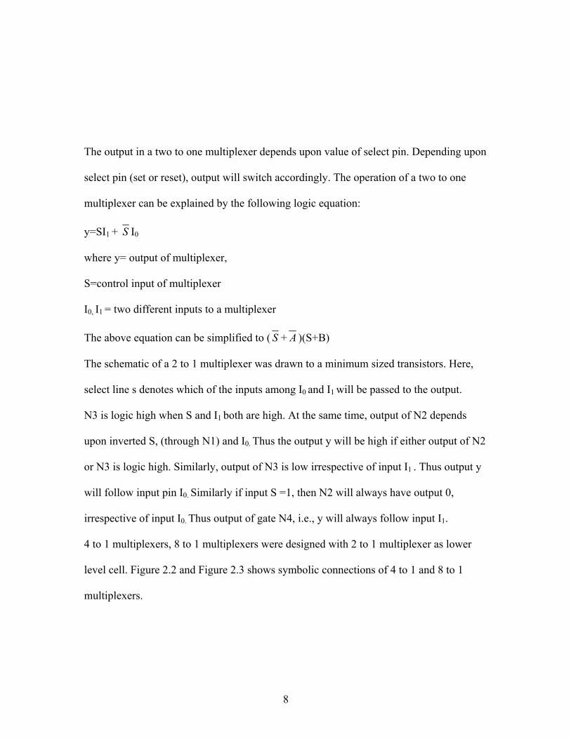
Figure 2-2 4 to 1 multiplexer
Figure 2-3 8 to 1 multiplexer
In figure 2.2, M1, M2 and M3 are single bit 2 to 1 multiplexer. S0 and S1 represent
control bits for selecting one out of four inputs. Similarly in figure 2.3, multiplexers M41
and M42 are 4 to 1 multiplexers with S<0:1> as input select lines. M4 is a 2 to 1 bit
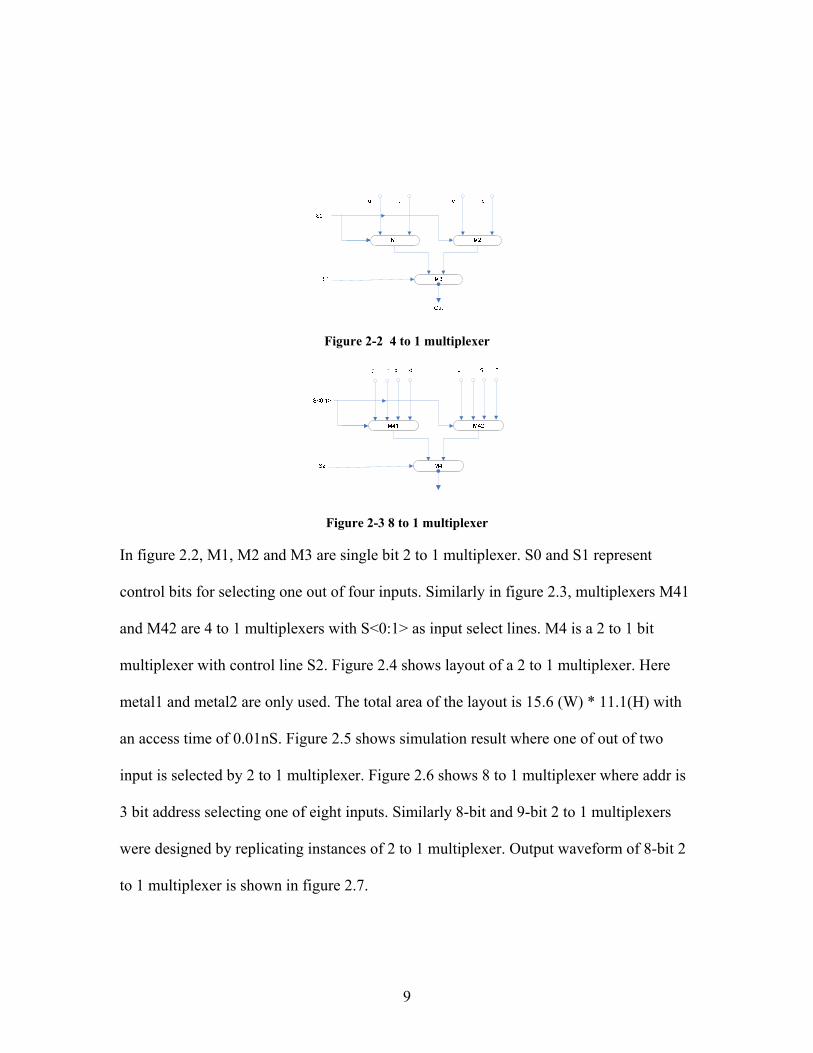
multiplexer with control line S2. Figure 2.4 shows layout of a 2 to 1 multiplexer. Here
metal1 and metal2 are only used. The total area of the layout is 15.6 (W) * 11.1(H) with
an access time of 0.01nS. Figure 2.5 shows simulation result where one of out of two
input is selected by 2 to 1 multiplexer. Figure 2.6 shows 8 to 1 multiplexer where addr is
3 bit address selecting one of eight inputs. Similarly 8-bit and 9-bit 2 to 1 multiplexers
were designed by replicating instances of 2 to 1 multiplexer. Output waveform of 8-bit 2
to 1 multiplexer is shown in figure 2.7.
10
Figure 2-4 Layout of a 2 to 1 multiplexer
Figure 2-5 Testing 2 to 1 multiplexer

11
Figure 2-6 8 to 1 multiplexer
Figure 2-7 8-bit 2 to 1 multiplexer
Table 2.1 shows comparison with size and area of different multiplexers used.
12
Table 2-1 Comparison of Multiplexer delays and layout area
Type Delay(in nS) Area(W in um * H in um)
1-bit 2 to 1 multiplexer 0.01 15.6*11.1
4 to 1 multiplexer 0.01 24.6*38.4
8-bit 2 to 1 multiplexer 0.01 18.15*80.55
9-bit 2 to 1 multiplexer 0.01 18.15*95.55
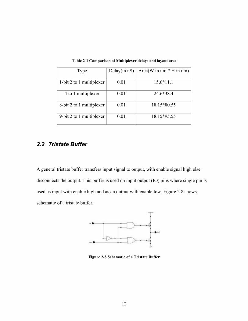
2.2 Tristate Buffer
A general tristate buffer transfers input signal to output, with enable signal high else
disconnects the output. This buffer is used on input output (IO) pins where single pin is
used as input with enable high and as an output with enable low. Figure 2.8 shows
schematic of a tristate buffer.
Figure 2-8 Schematic of a Tristate Buffer

13
The output is al a floating state when both pmos and nmos transistors are turned off. It
will be like open circuit and thus passing an ideal zero current through the output i.e.
keeping impedance, Z=V/I ∞.
When enable signal is high, the output is followed by the input. If logic high is to
be passed, then output will follow through the pmos transistor. If a logic zero is to be
transferred, output is followed through nmos transistor. A floating state is said to occur
only when enable is reset, i.e. both the transistors driving the output to a pin are turned
off. Figure 2.9 shows layout of a tristate buffer. The total delay of the circuit was 0.01nS
with a total layout area of 14.40(W) * 19.4(H).
Figure 2-9 Layout of a tristate buffer
14
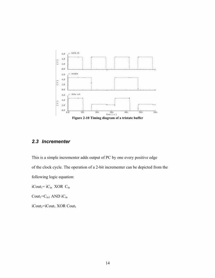
Figure 2-10 Timing diagram of a tristate buffer
2.3 Incrementer This is a simple incrementer adds output of PC by one every positive edge of the clock cycle. The operation of a 2-bit incrementer can be depicted from the
following logic equation:
iCout1= iCin XOR Cin
Cout1=Cin1 AND iCin
iCout2=iCout1 XOR Cout1
15
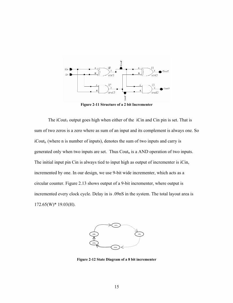
Figure 2-11 Structure of a 2 bit Incrementer
The iCout1 output goes high when either of the iCin and Cin pin is set. That is
sum of two zeros is a zero where as sum of an input and its complement is always one. So
iCoutn (where n is number of inputs), denotes the sum of two inputs and carry is
generated only when two inputs are set. Thus Coutn is a AND operation of two inputs.
The initial input pin Cin is always tied to input high as output of incrementer is iCin,
incremented by one. In our design, we use 9-bit wide incrementer, which acts as a
circular counter. Figure 2.13 shows output of a 9-bit incrementer, where output is
incremented every clock cycle. Delay in is .09nS in the system. The total layout area is
172.65(W)* 19.03(H).
Figure 2-12 State Diagram of a 8 bit incrementer
01h
1Fh
FEh
FFh
00h

16
Figure 2-13 Output of 9-bit incrementer
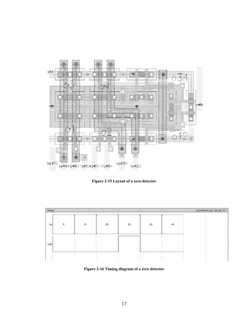
2.4 Zero Detector Output of a zero detector goes high when all 8-bit inputs are zero. The delay of the total
circuit is proportional to log2N, where N is number of stages. Figure 2.14 shows
schematic diagram of a zero detector. Total delay of a zero detector is 0.09nS. Total
layout area is 34.2(W)* 21.00(H). Figure 2.16 shows operation of a zero detector.
Figure 2-14 Schematics of a zero detector
17
Figure 2-15 Layout of a zero detector
Figure 2-16 Timing diagram of a zero detector
18
2.5 D latch Latches are level triggered asynchronous sequential circuits containing one feedback
which is equivalent to two asynchronous states. D-latch is an asynchronous sequential
circuit specified by the following functional table:
Table 2-2 D latch functional table
Clock Operation
0 Q<=Q Hold
1 Q<=D Load
Next state output, Qi+1 = clock . Qi + clock.Di
where Qi=output of present state,
Di=input of present state,
Qi+1=output of next state
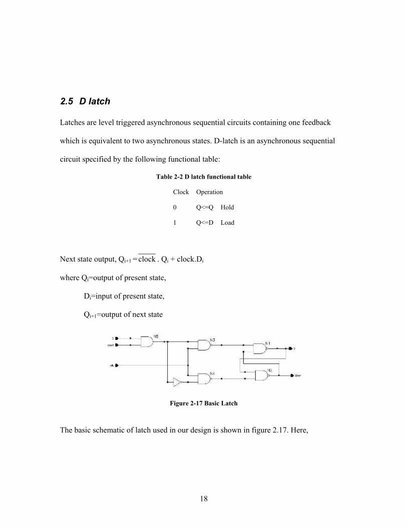
Figure 2-17 Basic Latch
The basic schematic of latch used in our design is shown in figure 2.17. Here,
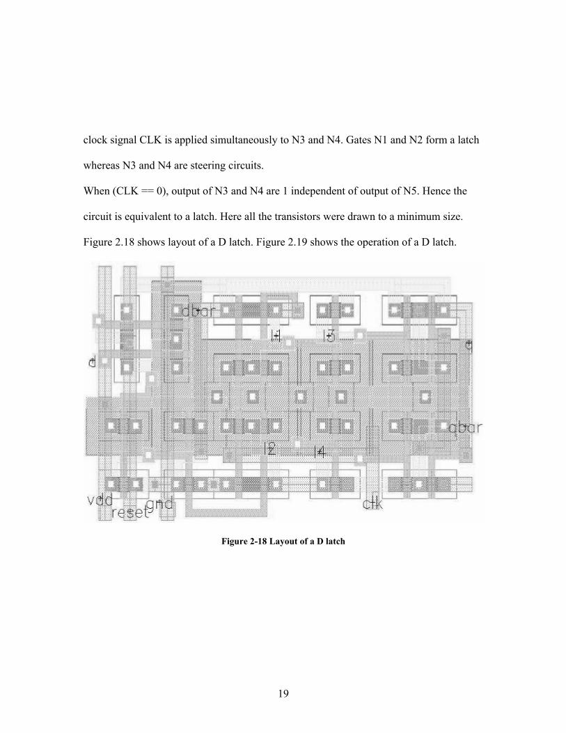
19
clock signal CLK is applied simultaneously to N3 and N4. Gates N1 and N2 form a latch
whereas N3 and N4 are steering circuits.
When (CLK == 0), output of N3 and N4 are 1 independent of output of N5. Hence the
circuit is equivalent to a latch. Here all the transistors were drawn to a minimum size.
Figure 2.18 shows layout of a D latch. Figure 2.19 shows the operation of a D latch.
Figure 2-18 Layout of a D latch
20
Figure 2-19 Output of a D latch
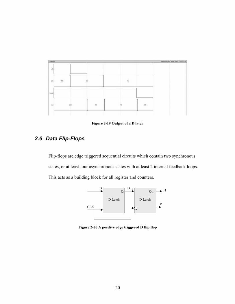
2.6 Data Flip-Flops
Flip-flops are edge triggered sequential circuits which contain two synchronous
states, or at least four asynchronous states with at least 2 internal feedback loops.
This acts as a building block for all register and counters.
Figure 2-20 A positive edge triggered D flip flop
CLK
Di+1Di
D Latch
D Latch
Qi Qi+1 Q
P

21
Figure 2-21 State diagram of a positive edge triggered D-type Flip-flop
There are four states coded by 2-bit binary words which represent two state signals, P and
Q. There are two input signals, D (data) and CLK (clock). Both state signals can be used
as outputs and here, the Q signal being of principal interest. The expected behavior is that
during rising edge of the clock signal, 1-bit data from input D is loaded into the flip-flop.
, i.e. Q<=D. Outside the rising edge of the clock signal, the state Q is to be unchanged.
Figure 2-23 shows IRSIM response of an 8-bit D type flip-flop and its corresponding
layout in Figure 2.22. Worst case delay observed was 0.5nS with total of 290.4(W) *
41.1(H) of a single bit D flip-flop.
Figure 2-22 Layout of 8-bit D type flip-flop
CLKCLK
CLK & D
CLK & D
CLKCLK
CLK
C
LK &
D
CLK
C
LK &
D
P Q 0 0
P Q 0 1
P Q 1 1
P Q 1 0

22
Figure 2-23 Simulation of 8-bit D type flip-flop
2.7 Ring Oscillator
A ring oscillator is realized by placing an odd number of inverters in a loop. This is
because of circuit latch occurring when numbers of inverters are even.
Figure 2-24 Ring Oscillator
Let us analyze a circuit with three stage ring oscillator as shown in Figure 2-24.
If it is assumed initially that voltage at each node of this circuit is equal, and there is no
noise, the circuit would not oscillate and remain in same stage forever. However, this is
not the ideal case as node voltages are different and there is always noise in the circuit.
Vx Vy Vz
23
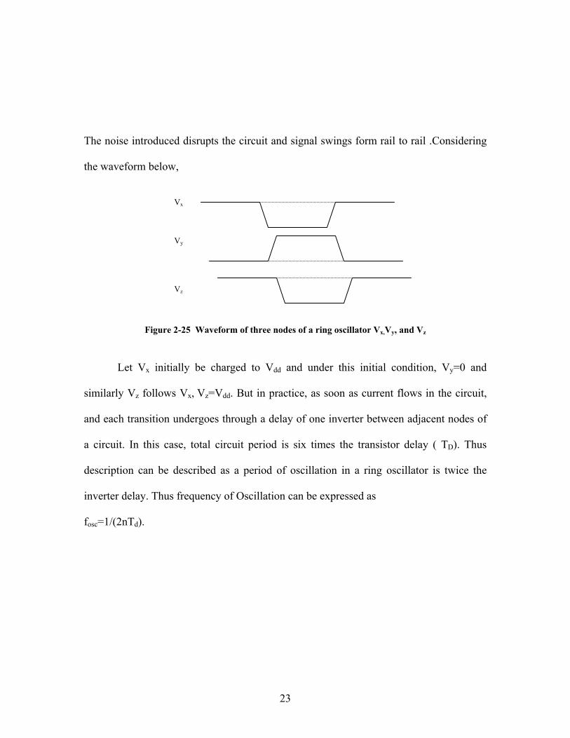
The noise introduced disrupts the circuit and signal swings form rail to rail .Considering
the waveform below,
Figure 2-25 Waveform of three nodes of a ring oscillator Vx,Vy, and Vz
Let Vx initially be charged to Vdd and under this initial condition, Vy=0 and
similarly Vz follows Vx, Vz=Vdd. But in practice, as soon as current flows in the circuit,
and each transition undergoes through a delay of one inverter between adjacent nodes of
a circuit. In this case, total circuit period is six times the transistor delay ( TD). Thus
description can be described as a period of oscillation in a ring oscillator is twice the
inverter delay. Thus frequency of Oscillation can be expressed as
fosc=1/(2nTd).
Figure 2-26 shows layout of a ring oscillator and Figure 2-27 shows oscillator output waveform.
Figure 2-26 Layout of a ring oscillator
Figure 2-27 Ring oscillator output
Vx Vy Vz

24
2.8 Arithmetic Logic Unit Arithmetic logic unit comprises of circuitry for arithmetic and logical operations. The
arithmetic unit comprises of a full adder capable of addition, subtraction (by two’s
complement method) and a logical unit for complement, exclusive OR, AND and NOT
operation.
Figure 2-28 Block Diagram of a full adder
A full adder is capable of adding input data and one carry from previous significant bit.
In Figure 2-28 above, A and B are adder inputs, Cin is the carry input , S is the sum
output, and Cout the carry output.
2.8.1 Single-Bit Adders The simplest approach of an adder implemented is by combinational gates for
majority of functions. The logic equation for generating Sum and carry signals are:
Cout=A.B + A. Cin + B. Cin
Sum, S= A.B.Cin + A. B . Cin + A B Cin + A B Cin
Cout Sum
A
B
Cin
Full Adder

25
which may be factorized as:
Cin(A.B + A . B ) + Cin (A. B + A .B)
= A XOR B XOR Cin
Table .2-3 Binary Addition
An eight bit parallel full adder is constructed by cascading eight one bit adder
cells in parallel. The inputs A and B are 8-bit. In each of these cells, the Cout pin of lower
order cell is connected to Cin of higher order cell. This operation can be expressed with
the following logic equation:
Cini+1=Couti , where i is the ith stage.
The nth bit of the Sum, Sn indicates result, while the nth Carry signal (Coutn) indicates
whether an overflow has occurred. As the carry out signal Cout is used to generate the
sum (S), sum (S) will be delayed with respect to Carry signal. For the case of eight bit
parallel adder, the total delay of eight stages, T8=8 * Tc, where Tc is the delay of one carry
stage, T8 is total delay time of eight stages. For AND logical operation, a 2 input NAND
gate is used as a basic cell. Output of the NAND gate is used in a multiplexer to select the
A 0 0 0 0 1 1 1 1
B 0 0 1 1 0 0 1 1
Cin 0 1 0 1 0 1 0 1
Cout S 0 0 0 1 01 1 0 0 1 1 0 1 0 1 1

26
desired output. Here, transistors are made as minimum in size as possible, to minimize
delay. For OR type of instructions, a 2 input NOR gate is used with its output connected
to 4 to 1 multiplexer. A XOR operation was performed with two of three inputs(A and
B). Inputs A and B will be in finite state and Cout and Cin signals will be forced to have
logic value zero. XOR operation was equivalent to a ADD instruction with Cout forced to
zero. Figure 3.18 below shows how carry generated is blocked in a XOR operation.
Figure 3.18 Carry propagation signal blocked for XOR operation
In the above figure, N1 has two active low inputs Cout_in and sel_fa . Sel_fa
active indicates that Carryout of the first stage Couti ,(in ith stage ) is propagated to the
next stage as Cini+1. Arithmetic operations (addition, subtraction, MOV, IOR) all are
processed in the arithmetic block.
Figure 3.19 A input pin for ALU
27
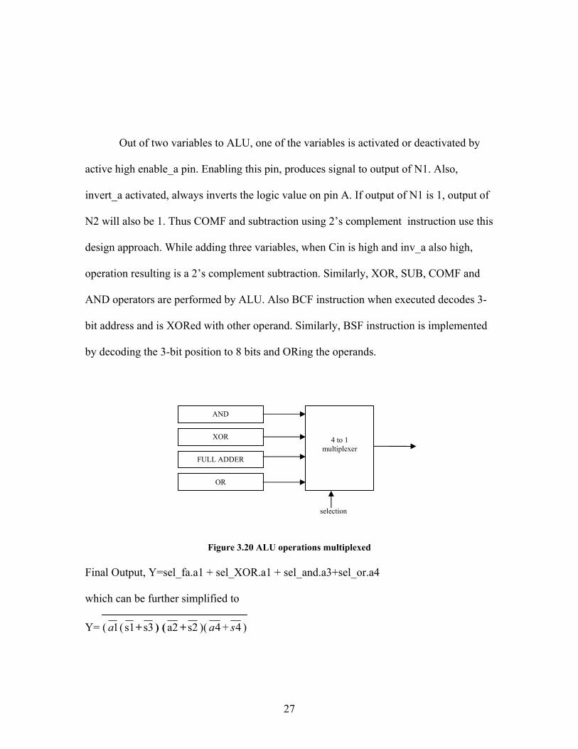
Out of two variables to ALU, one of the variables is activated or deactivated by
active high enable_a pin. Enabling this pin, produces signal to output of N1. Also,
invert_a activated, always inverts the logic value on pin A. If output of N1 is 1, output of
N2 will also be 1. Thus COMF and subtraction using 2’s complement instruction use this
design approach. While adding three variables, when Cin is high and inv_a also high,
operation resulting is a 2’s complement subtraction. Similarly, XOR, SUB, COMF and
AND operators are performed by ALU. Also BCF instruction when executed decodes 3-
bit address and is XORed with other operand. Similarly, BSF instruction is implemented
by decoding the 3-bit position to 8 bits and ORing the operands.
Figure 3.20 ALU operations multiplexed Final Output, Y=sel_fa.a1 + sel_XOR.a1 + sel_and.a3+sel_or.a4
which can be further simplified to
Y= ( 1a ( s1+ s3 ) ( a2 + s2 )( 4a + 4s )
4 to 1 multiplexer
AND
XOR
FULL ADDER
OR
selection
28
where 1a = _outfull_adder
a2 = and_out
s1= sel_fa
s2 =sel_and
s3 = sel_xor
4s = sel_or
4a = out_or
Final output Y, is constructed for the above logic equation for desired output with
minimum transistor size. Higher order ALU cells are constructed by joining Cin of higher
stages to Cout of lower stages. Figure 2-30 shows operation of a 8 bit ALU. Total area of
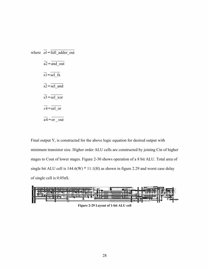
single bit ALU cell is 144.6(W) * 11.1(H) as shown in figure 2.29 and worst case delay
of single cell is 0.05nS.
Figure 2-29 Layout of 1-bit ALU cell
29
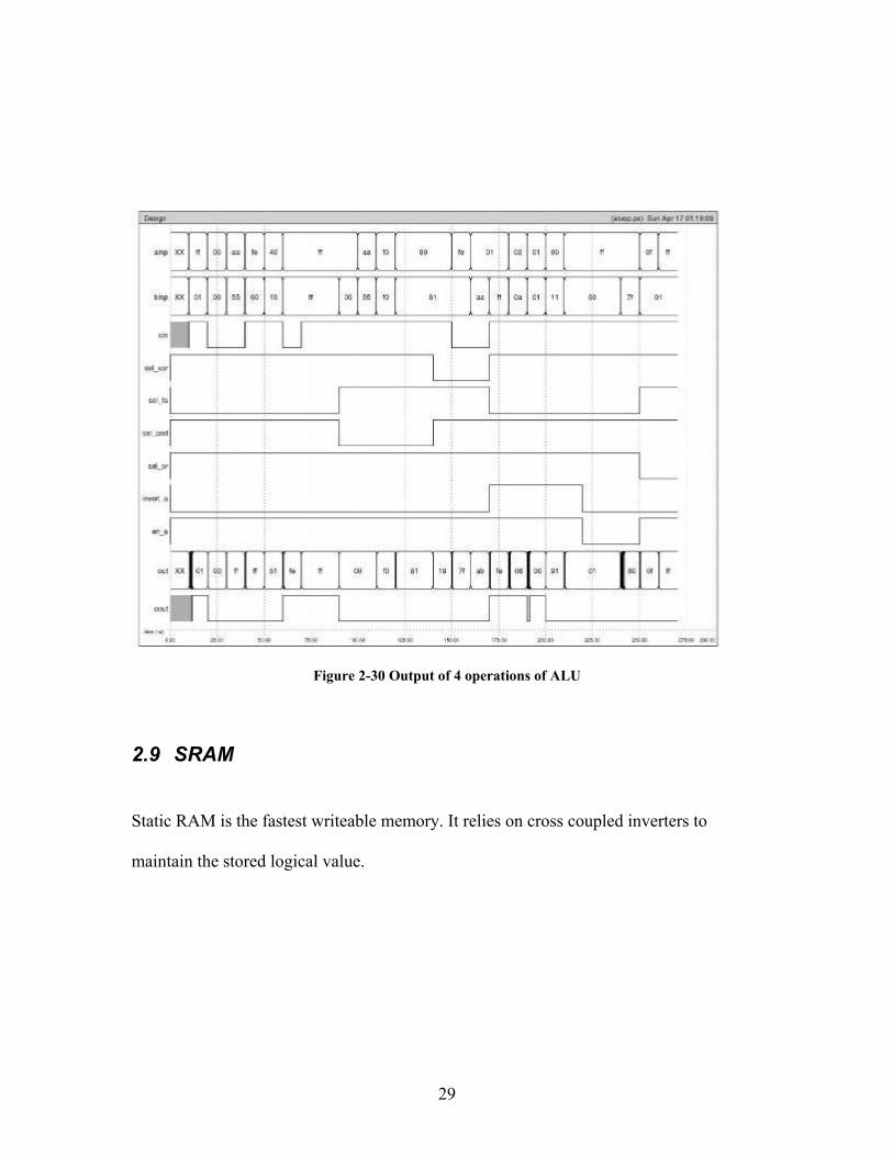
Figure 2-30 Output of 4 operations of ALU
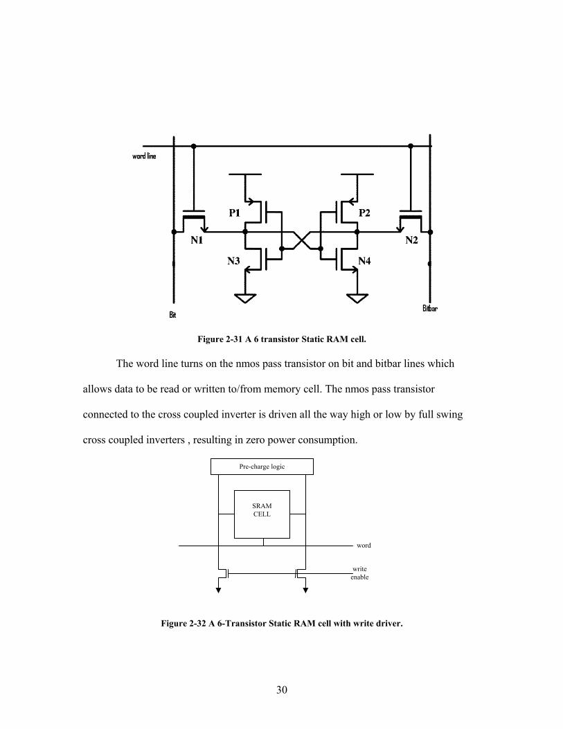
2.9 SRAM Static RAM is the fastest writeable memory. It relies on cross coupled inverters to
maintain the stored logical value.
30
Figure 2-31 A 6 transistor Static RAM cell. The word line turns on the nmos pass transistor on bit and bitbar lines which
allows data to be read or written to/from memory cell. The nmos pass transistor
connected to the cross coupled inverter is driven all the way high or low by full swing
cross coupled inverters , resulting in zero power consumption.
Figure 2-32 A 6-Transistor Static RAM cell with write driver.
SRAM CELL
Pre-charge logic
word
write enable

31
Theorey of operation
i) Write Operation
The transistors N1 and N2 enabled, allows data and its complement to be moved
to bit and bitbar lines. The word line is asserted with a high voltage. The bit or bitbar
lines are driven to Vss and Vdd-VT respectively where VT = transient voltage. Considering
a case of writing on a previously stored zero value, cell has to be pulled above the RAM
cell inverter threshold , as well as cell bar pulled well below cell threshold voltage.
ii) Read Operation
While reading, small transistors in the memory cell must drive large capacitance on bit
and bitbar lines. The bit line capacitance is dominated by contribution of drain of pass
transistors from the entire column of memory cell connected to the bit lines. Pre-charge
must be done before each read and write cycle starting, to overpower result of previously
stored value stored on bit and bitbar lines. Here, data is latched through the bitbar line an
data is read only through the bit line. Initially, cell and cellbar, the two cross-coupled
inverters were set to Vdd and Gnd respectively. Figure 2-34 shows waveform of static
RAM while reading and writing. Here, bit line is isolated and not pre-charged, so we can
see a large decay in time for the charge stored. In Figure 2-34, Vwrite is the write signal,
VwordA is the word enable signal, Vpre is the precharge. VbitA and VbitAbar show
signals at bit and bitbar lines.

32
Figure 2-33 SRAM cell layout
Figure 2-34 SRAM test result
33
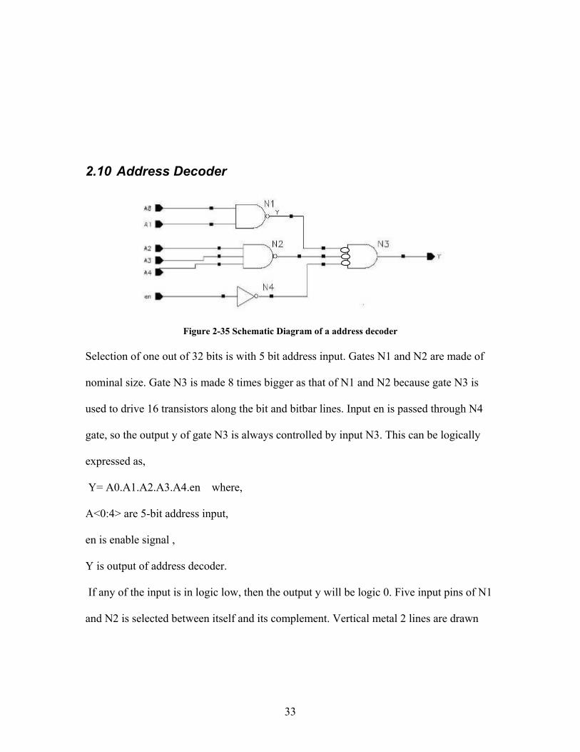
2.10 Address Decoder
Figure 2-35 Schematic Diagram of a address decoder Selection of one out of 32 bits is with 5 bit address input. Gates N1 and N2 are made of
nominal size. Gate N3 is made 8 times bigger as that of N1 and N2 because gate N3 is
used to drive 16 transistors along the bit and bitbar lines. Input en is passed through N4
gate, so the output y of gate N3 is always controlled by input N3. This can be logically
expressed as,
Y= A0.A1.A2.A3.A4.en where,
A<0:4> are 5-bit address input,
en is enable signal ,
Y is output of address decoder.
If any of the input is in logic low, then the output y will be logic 0. Five input pins of N1
and N2 is selected between itself and its complement. Vertical metal 2 lines are drawn

34
each separated by 0.9 µm each of 1.2µm width. Poly lines are drawn and 1.2 µm wide
M1 spread between two M2 lines as shown in figure 2.36 below. The layout area of each
individual address decoder is 46.65(W) * 13.20(H) with an access delay of 0.02ns.
Figure 2-36 Layout of single bit address decoder
2.11 Read/Write circuitry for SRAM Input pins rd/wr selects read or write operation. When read mode is selected, i.e. rd/wr
=1, and din=1, output of both N1 and N2 is zero disabling N4 and N5. This implies that,
during read operation, bit and bitbar lines are isolated. Similarly, when rd/wr=1, N4 and
N5 are turned on or off depending upon the din input. Figure 2.37 shows the circuitry for
read/write operation. Total area of the read write circuitry is 12.15(W) * 35.85(H).Figure
2.38 shows layout of read/write circuitry.
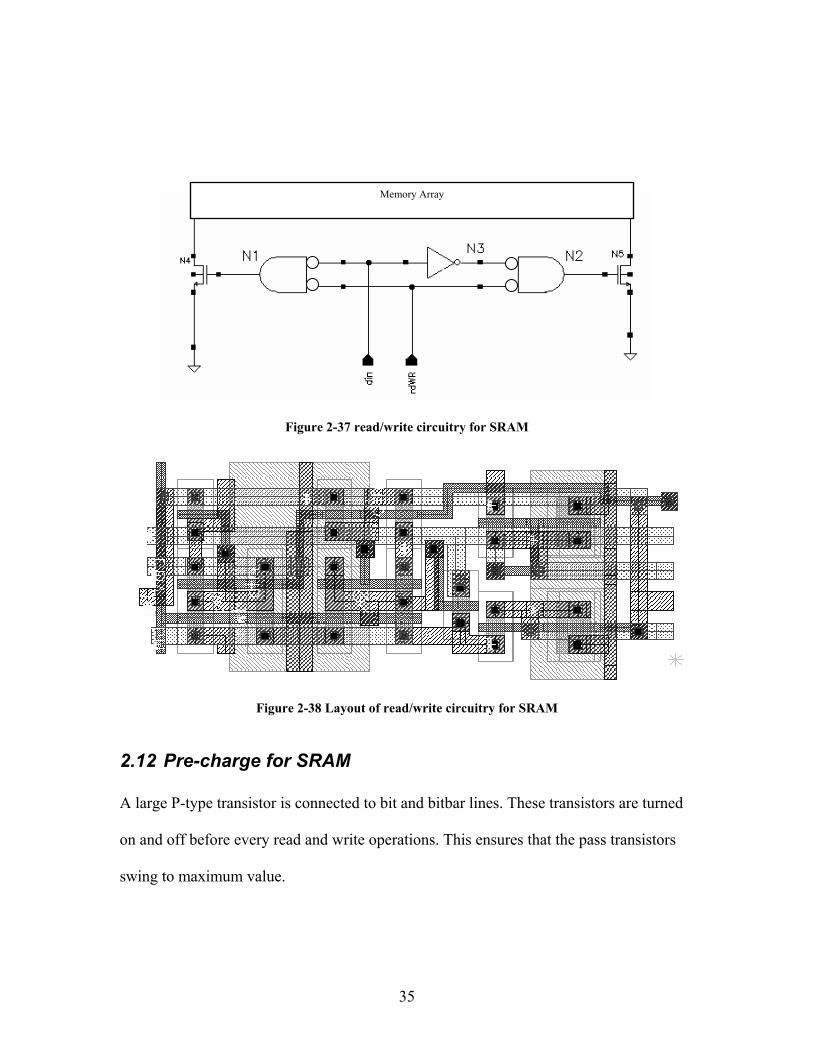
35
Figure 2-37 read/write circuitry for SRAM
Figure 2-38 Layout of read/write circuitry for SRAM
2.12 Pre-charge for SRAM A large P-type transistor is connected to bit and bitbar lines. These transistors are turned
on and off before every read and write operations. This ensures that the pass transistors
swing to maximum value.
Memory Array
36
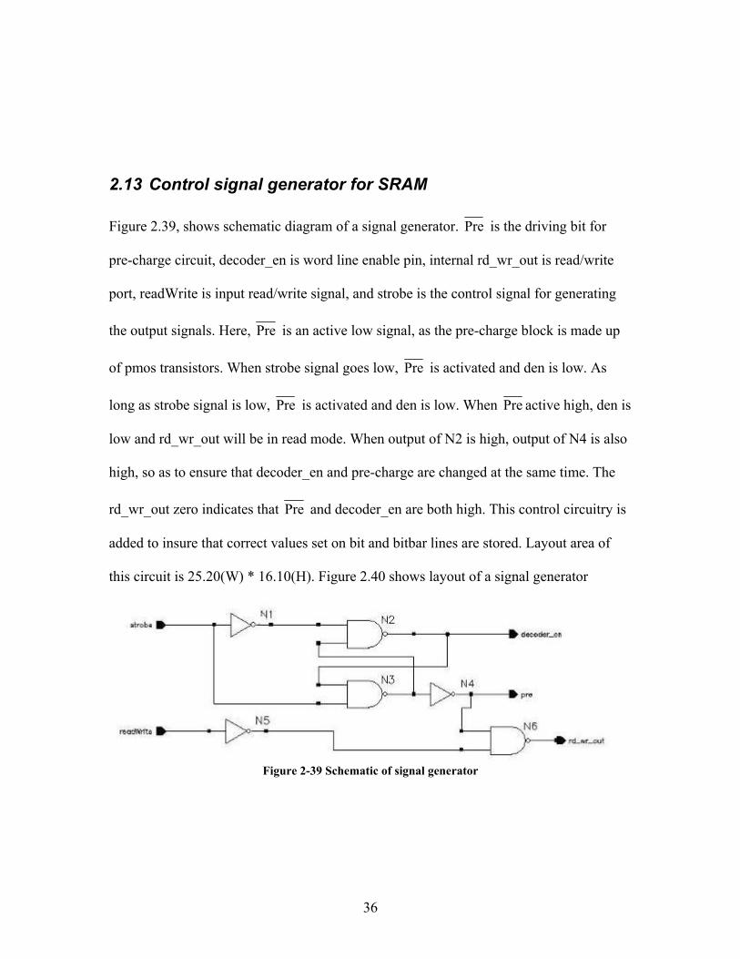
2.13 Control signal generator for SRAM Figure 2.39, shows schematic diagram of a signal generator. Pre is the driving bit for
pre-charge circuit, decoder_en is word line enable pin, internal rd_wr_out is read/write
port, readWrite is input read/write signal, and strobe is the control signal for generating
the output signals. Here, Pre is an active low signal, as the pre-charge block is made up
of pmos transistors. When strobe signal goes low, Pre is activated and den is low. As
long as strobe signal is low, Pre is activated and den is low. When Pre active high, den is
low and rd_wr_out will be in read mode. When output of N2 is high, output of N4 is also
high, so as to ensure that decoder_en and pre-charge are changed at the same time. The
rd_wr_out zero indicates that Pre and decoder_en are both high. This control circuitry is
added to insure that correct values set on bit and bitbar lines are stored. Layout area of
this circuit is 25.20(W) * 16.10(H). Figure 2.40 shows layout of a signal generator
Figure 2-39 Schematic of signal generator

37
Figure 2-40 Layout of signal generator
Figure 2-41 Timing Diagram of signal generator
38
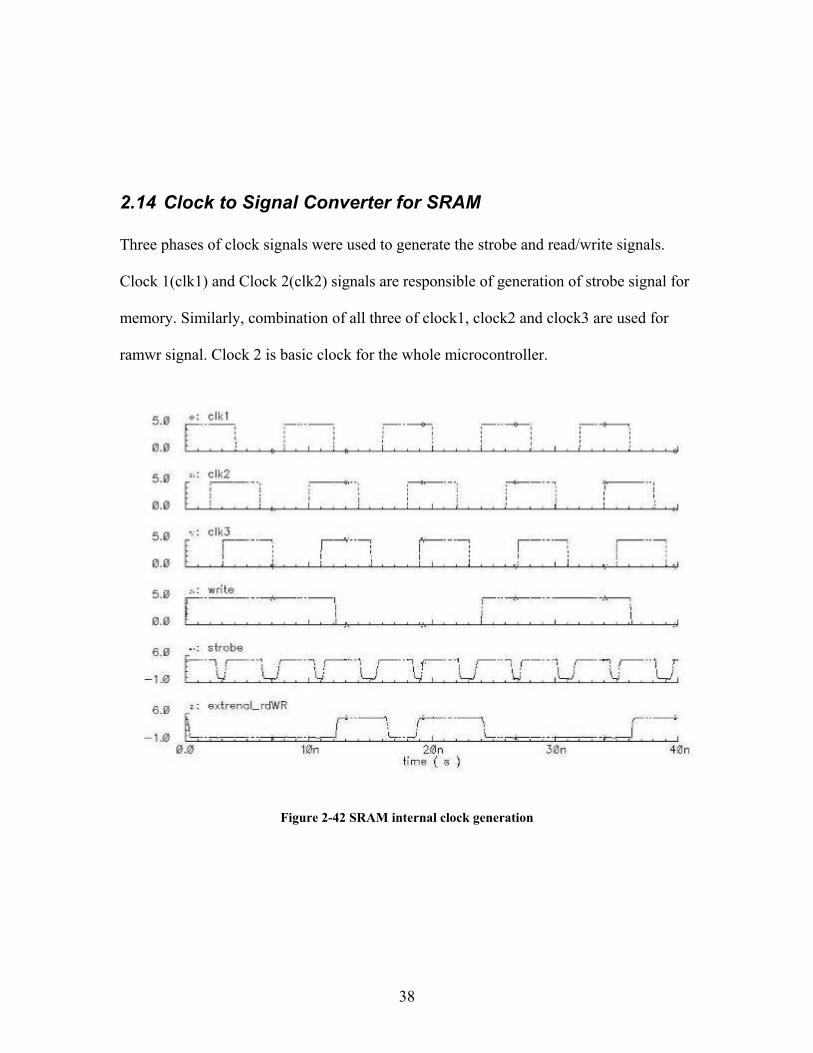
2.14 Clock to Signal Converter for SRAM Three phases of clock signals were used to generate the strobe and read/write signals.
Clock 1(clk1) and Clock 2(clk2) signals are responsible of generation of strobe signal for
memory. Similarly, combination of all three of clock1, clock2 and clock3 are used for
ramwr signal. Clock 2 is basic clock for the whole microcontroller.
Figure 2-42 SRAM internal clock generation
39
2.15 Counter
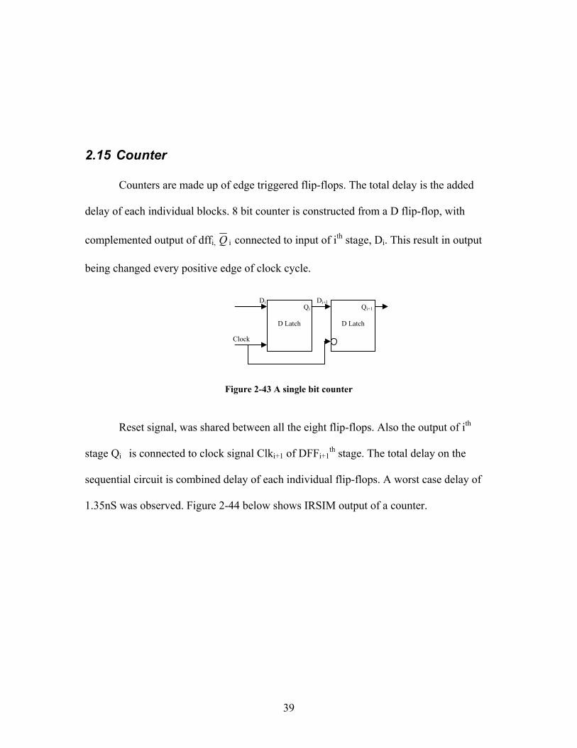
Counters are made up of edge triggered flip-flops. The total delay is the added
delay of each individual blocks. 8 bit counter is constructed from a D flip-flop, with
complemented output of dffi, Q i connected to input of ith stage, Di. This result in output
being changed every positive edge of clock cycle.
Figure 2-43 A single bit counter
Reset signal, was shared between all the eight flip-flops. Also the output of ith
stage Qi is connected to clock signal Clki+1 of DFFi+1th stage. The total delay on the
sequential circuit is combined delay of each individual flip-flops. A worst case delay of
1.35nS was observed. Figure 2-44 below shows IRSIM output of a counter.
Clock
Di+1Di
D Latch
D Latch
Qi Qi+1
40
Figure 2-44 IRSIM output of a 8 bit counter
2.16 Status Register Status Register is a eight bit wide register which contains present status of ALU,
comprising of arithmetic, logical as well as RESET status. The status register is
destination of many instructions. If STATUS register is destination for an instruction that
affects Z, DC or C bits, these bits are set or cleared according to device logic. Bits TO
and PD are not writeable. The register is mapped to special purpose memory SRAM at
location 03h.
TO PD Z DC C
Figure 2-45 Status Register
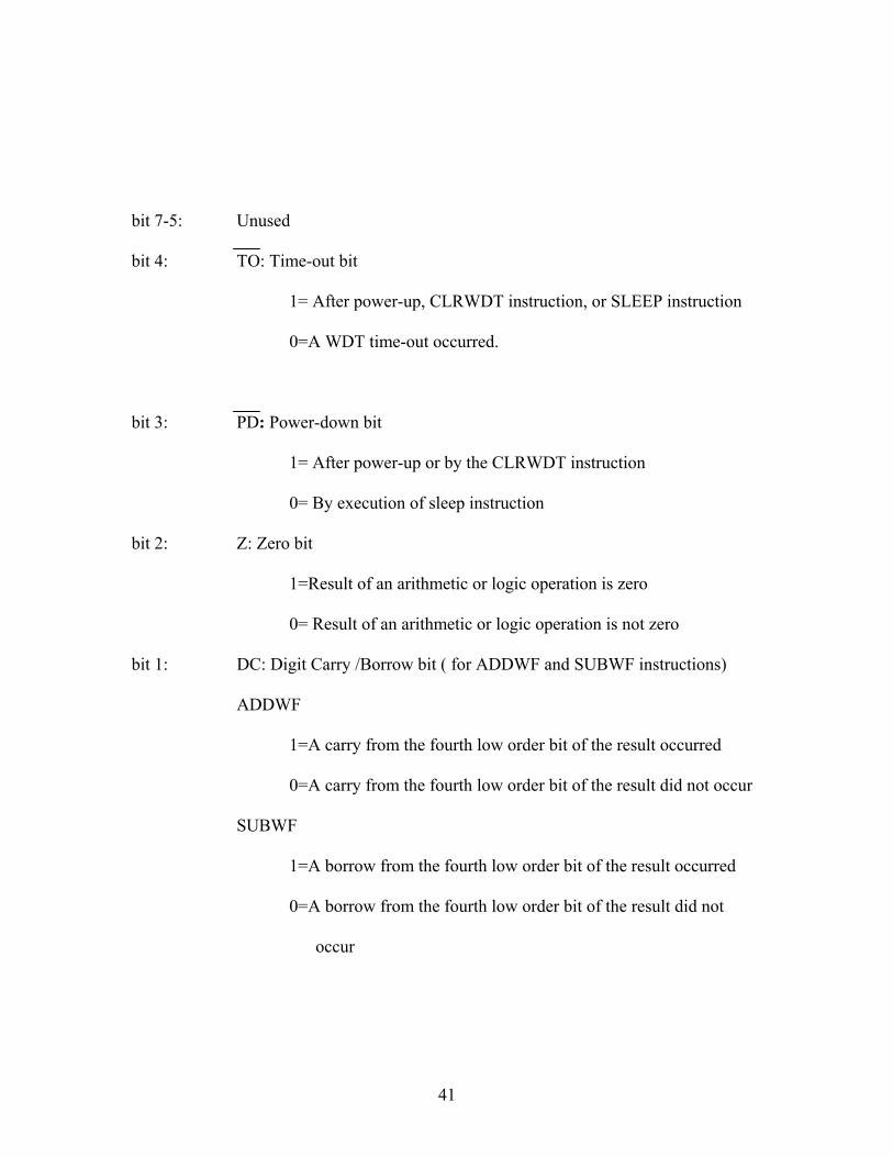
41
bit 7-5: Unused
bit 4: TO: Time-out bit
1= After power-up, CLRWDT instruction, or SLEEP instruction
0=A WDT time-out occurred.
bit 3: PD: Power-down bit
1= After power-up or by the CLRWDT instruction
0= By execution of sleep instruction
bit 2: Z: Zero bit
1=Result of an arithmetic or logic operation is zero
0= Result of an arithmetic or logic operation is not zero
bit 1: DC: Digit Carry /Borrow bit ( for ADDWF and SUBWF instructions)
ADDWF
1=A carry from the fourth low order bit of the result occurred
0=A carry from the fourth low order bit of the result did not occur
SUBWF
1=A borrow from the fourth low order bit of the result occurred
0=A borrow from the fourth low order bit of the result did not
occur

42
bit 0: C: Carry/ borrow bit (for ADDWF, SUBWF, RRF and RLF instructions)
ADDWF
1= A carry occurred
0=A carry did not occur
SUBWF
1=A borrow did not occur
0=A borrow occurred
RRF,RLF
Loaded with LSb or MSb , respectively
2.17 Option Register Option register is a 6-bit, write only register. It contains various control bits to
configure Timer 0 /WDT prescalar and Timer 0 module. The option register is connected
to the accumulator and it is addressed by OPTION instruction. A reset signal, RESET
sets all pins of OPTION register high.
T0CS T0SE PSA PS2 PS1 PS0
Figure 2-46 Bit allocation in a Option register
bit 7-6: Unimplemented
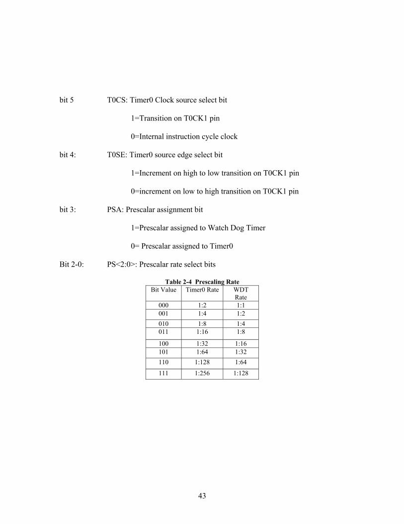
43
bit 5 T0CS: Timer0 Clock source select bit
1=Transition on T0CK1 pin
0=Internal instruction cycle clock
bit 4: T0SE: Timer0 source edge select bit
1=Increment on high to low transition on T0CK1 pin
0=increment on low to high transition on T0CK1 pin
bit 3: PSA: Prescalar assignment bit
1=Prescalar assigned to Watch Dog Timer
0= Prescalar assigned to Timer0
Bit 2-0: PS<2:0>: Prescalar rate select bits
Table 2-4 Prescaling Rate Bit Value Timer0 Rate WDT
Rate 000 1:2 1:1 001 1:4 1:2 010 1:8 1:4 011 1:16 1:8
100 1:32 1:16 101 1:64 1:32 110 1:128 1:64
111 1:256 1:128
44
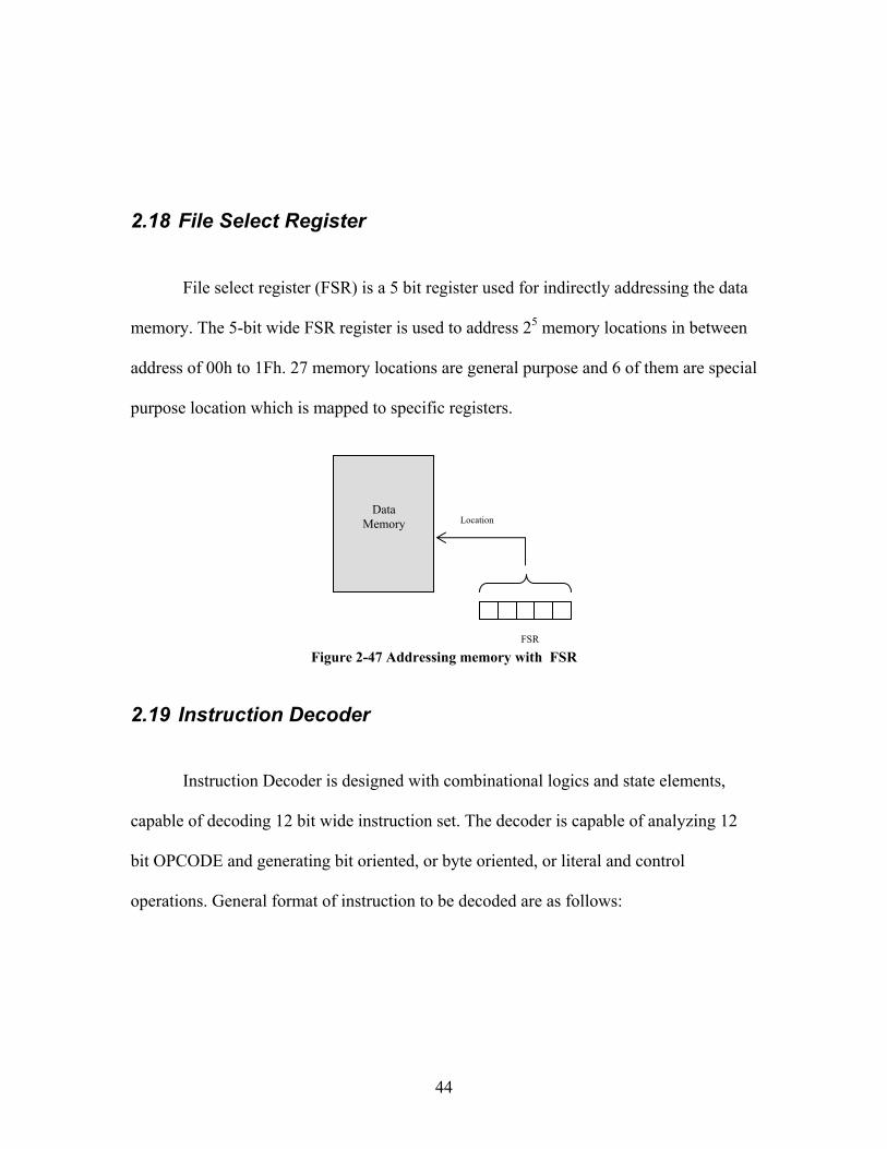
2.18 File Select Register
File select register (FSR) is a 5 bit register used for indirectly addressing the data
memory. The 5-bit wide FSR register is used to address 25 memory locations in between
address of 00h to 1Fh. 27 memory locations are general purpose and 6 of them are special
purpose location which is mapped to specific registers.
Figure 2-47 Addressing memory with FSR
2.19 Instruction Decoder Instruction Decoder is designed with combinational logics and state elements,
capable of decoding 12 bit wide instruction set. The decoder is capable of analyzing 12
bit OPCODE and generating bit oriented, or byte oriented, or literal and control
operations. General format of instruction to be decoded are as follows:
Data Memory
FSR
Location
45
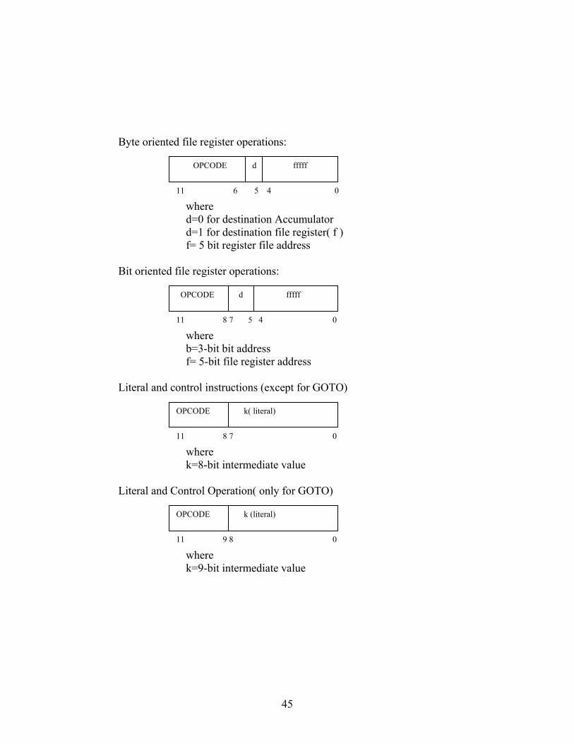
Byte oriented file register operations:
where
d=0 for destination Accumulator d=1 for destination file register( f ) f= 5 bit register file address Bit oriented file register operations:
where
b=3-bit bit address f= 5-bit file register address
Literal and control instructions (except for GOTO)
where
k=8-bit intermediate value
Literal and Control Operation( only for GOTO)
where k=9-bit intermediate value
11 9 8 0
OPCODE k (literal)
11 8 7 0
OPCODE k( literal)
11 8 7 5 4 0
OPCODE fffff d
11 6 5 4 0
OPCODE fffff d
46
Chapter 3
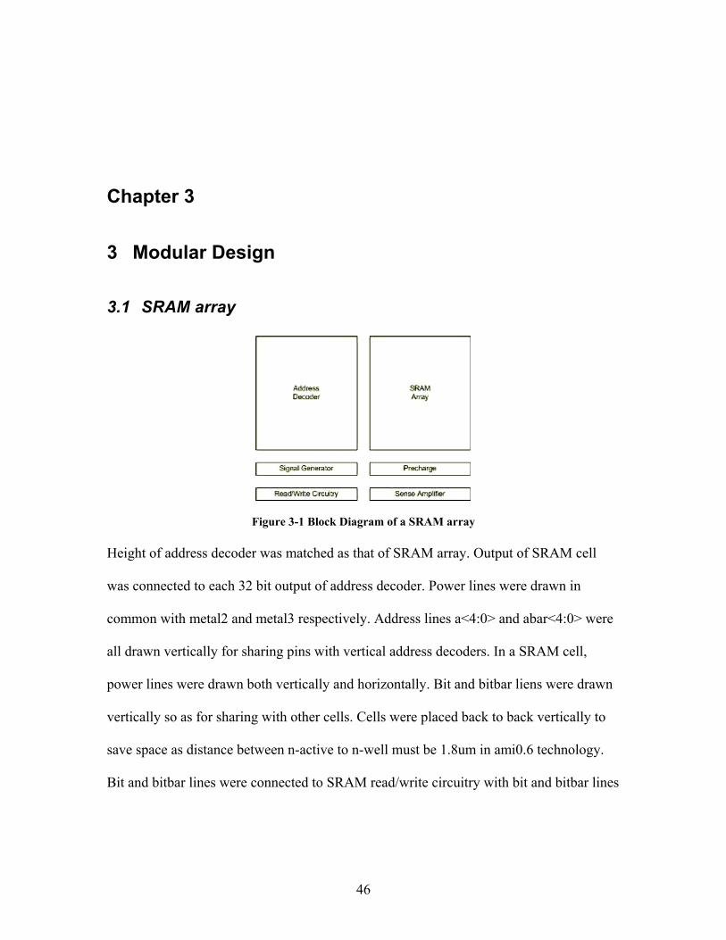
3 Modular Design
3.1 SRAM array
Figure 3-1 Block Diagram of a SRAM array Height of address decoder was matched as that of SRAM array. Output of SRAM cell
was connected to each 32 bit output of address decoder. Power lines were drawn in
common with metal2 and metal3 respectively. Address lines a<4:0> and abar<4:0> were
all drawn vertically for sharing pins with vertical address decoders. In a SRAM cell,
power lines were drawn both vertically and horizontally. Bit and bitbar liens were drawn
vertically so as for sharing with other cells. Cells were placed back to back vertically to
save space as distance between n-active to n-well must be 1.8um in ami0.6 technology.
Bit and bitbar lines were connected to SRAM read/write circuitry with bit and bitbar lines
47
equally spaced. Width of read/write circuit was same as that of memory cell. The inputs
for read/write circuitry, read/write and data in were drawn vertically. Pre-charge was
placed right below the read/write circuitry. Below the address decoder, internal signal
generator was placed and data latch fro SRAM was placed right below the pre-charge
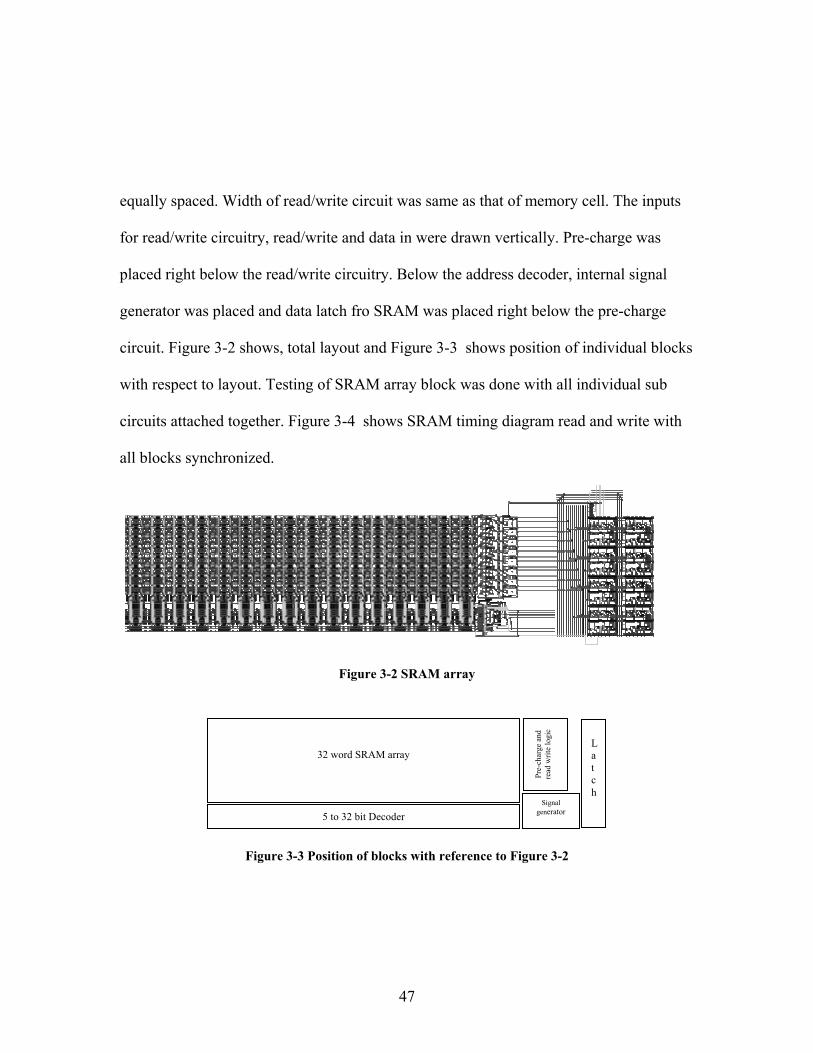
circuit. Figure 3-2 shows, total layout and Figure 3-3 shows position of individual blocks
with respect to layout. Testing of SRAM array block was done with all individual sub
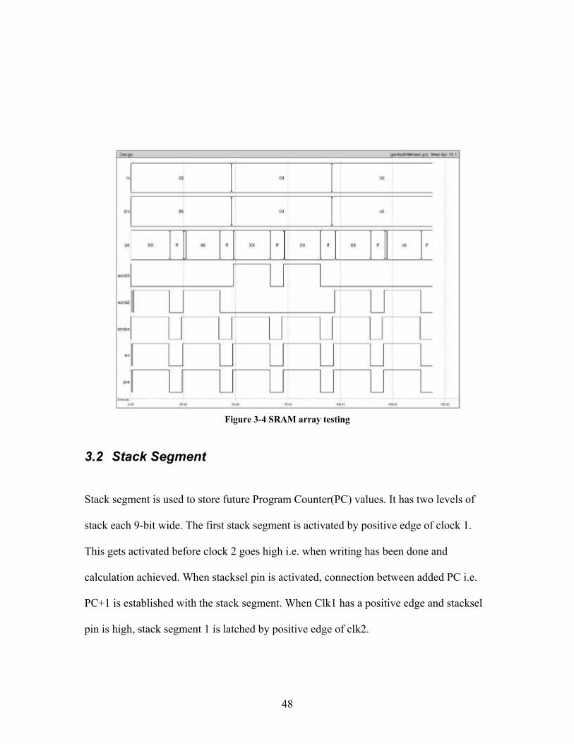
circuits attached together. Figure 3-4 shows SRAM timing diagram read and write with
all blocks synchronized.
Figure 3-2 SRAM array
Figure 3-3 Position of blocks with reference to Figure 3-2
32 word SRAM array
5 to 32 bit Decoder
Pre-
char
ge a
nd
read
writ
e lo
gic
Signal generator
Latch
48
Figure 3-4 SRAM array testing
3.2 Stack Segment Stack segment is used to store future Program Counter(PC) values. It has two levels of
stack each 9-bit wide. The first stack segment is activated by positive edge of clock 1.
This gets activated before clock 2 goes high i.e. when writing has been done and
calculation achieved. When stacksel pin is activated, connection between added PC i.e.
PC+1 is established with the stack segment. When Clk1 has a positive edge and stacksel
pin is high, stack segment 1 is latched by positive edge of clk2.
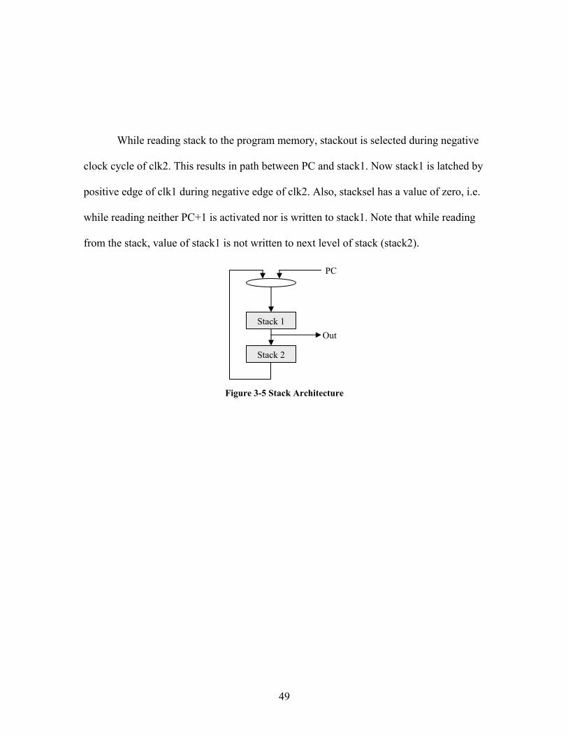
49
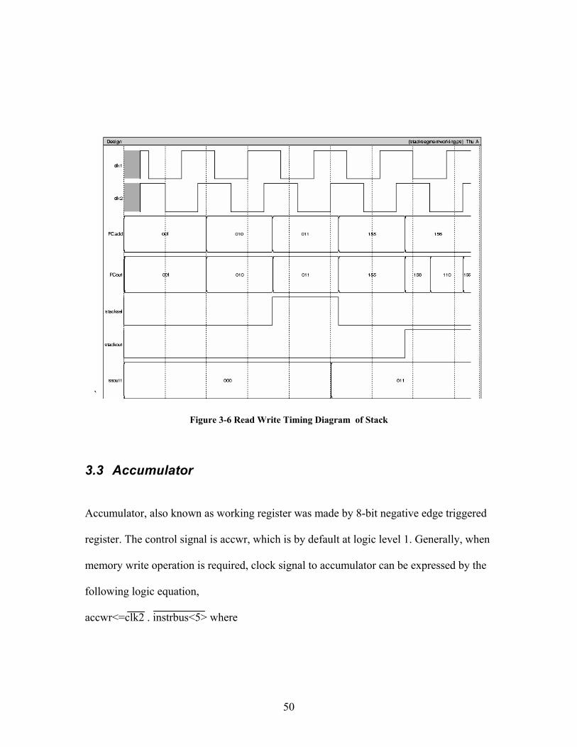
While reading stack to the program memory, stackout is selected during negative
clock cycle of clk2. This results in path between PC and stack1. Now stack1 is latched by
positive edge of clk1 during negative edge of clk2. Also, stacksel has a value of zero, i.e.
while reading neither PC+1 is activated nor is written to stack1. Note that while reading
from the stack, value of stack1 is not written to next level of stack (stack2).
Figure 3-5 Stack Architecture
Stack 1
Stack 2
PC
Out
50
`
Figure 3-6 Read Write Timing Diagram of Stack
3.3 Accumulator Accumulator, also known as working register was made by 8-bit negative edge triggered
register. The control signal is accwr, which is by default at logic level 1. Generally, when
memory write operation is required, clock signal to accumulator can be expressed by the
following logic equation,
accwr<=clk2 . instrbus<5> where
51
clk2 is clock signal for microcontroller,
instrbus<5> is fifth bit in instruction bus , which goes low while writing to accumulator,
accwr is accumulator clock signal.
Input to accumulator is either from ALU or from rotate or swap functional block
(selected by roate_en pin from instruction decoder). Output of accumulator is to memory,
IO ports, status register, OPTION register and ALU.
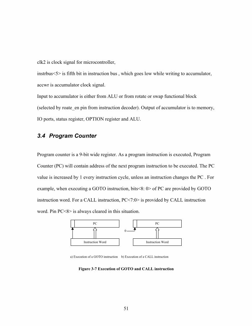
3.4 Program Counter
Program counter is a 9-bit wide register. As a program instruction is executed, Program
Counter (PC) will contain address of the next program instruction to be executed. The PC
value is increased by 1 every instruction cycle, unless an instruction changes the PC . For
example, when executing a GOTO instruction, bits<8: 0> of PC are provided by GOTO
instruction word. For a CALL instruction, PC<7:0> is provided by CALL instruction
word. Pin PC<8> is always cleared in this situation.
Figure 3-7 Execution of GOTO and CALL instruction
PC
Instruction Word
a) Execution of a GOTO instruction
PC
Instruction Word
0
b) Execution of a CALL instruction
52
3.5 Bit Test
This block is made up with single 8 to 1 bit multiplexer Address given by b bus<2:0>
will decode 1 out of eight bits and then transfer it to output BTout. Enable pin, btf_en ,
when selected , corresponding bit position value is transferred to BTout pin, else BTout
will always equal to zero.
3.6 Rotate and Swap
Rotate instructions, RLF and RRF uses 9-bit operands (8-bit memory data and Carry) to
rotate right or left controlled by rf pin. swapf_en enables the swap operation of lower
bits<3:0> with bits<7:4>. This block is connected to output of SRAM. Output of this
block is connected to a 8- bit multiplexer, where ALU_OUT bus is another input.
3.7 Input Output Port In this design, two ports are available, a 4-bit wide and a 8-bit wide. Both have
bidirectional bit by bit programmable pins.
53
Figure 3-8 Single bit Input Output Port
A tris input being set, ensures that the IO (Input Output) port is ready for read operation.
The RD_PORT signal is responsible for reading the IO port. While reading, the pmos and
nmos transistors are both turned off. Thus the signal captured only on the IO port is easily
transferred to the data bus.
When writing to the IO port, the tris signal is reset and data is latched through the
D bus. During write operation, WR signal set ensures that data is written to the latch. The
IO port is connected to the pads for external IO operation.
54
3.8 Timer 0 Module
3.8.1 Timer0 Register
This mode is selected by clearing T0CS bit, OPTION<5>. In timer mode, Timer0 will be
incrementing every instruction cycle. By writing values to TMR0 register, it can be used
as a timer. Counter mode is selected by setting the O0CS bit , in OPTION<5>. IN this
mode, Timer0 will increment either on every rising or falling edge of T0CK1 pin
determined by source edge select bit T0SC (OPTION<4>).Clearing T0SE selects right
edge. Prescalar may be used either by Timer) module or watchdog timer but not by both.
The prescalar assignment is software controlled by PSA(OPTION<3>). Clearing PSA bit
will assign prescalar to Timer0. the prescalar is unreachable. When prescalar is assigned
to Timer0 module, prescale rate of 1:2 , 1:4,1:8,1:16,1:32,1:64,1:128,1:256 are selectable.
3.8.2 Prescalar
An 8-bit counter is available as prescalar for Timer0 module or as postscalar for
watchdog timer. Prescalar may be used either by Timer) module or WDT but not by both.
The PSA and PS<2:0> bits of OPTION<3:0> determine prescalar assignment and
prescalar ratio.
55
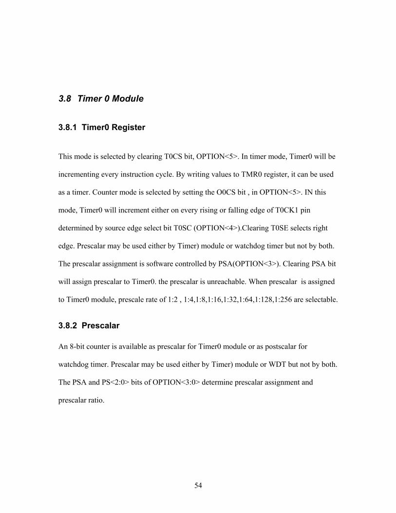
3.8.3 Watch Dog Timer
Figure 3-9 Timer0 module
Gate N1 determines positive or negative edge of clock to be used by XOR operation with
T0SE pin. T0SE pin can change input clock inverted so as output clock can be used as
positive edge triggered or negative edge triggered sub-system.
Figure 3-10 Generation of Positive edge or negative edge clock for Timer0 module
Input clock TOSE Output
N1
M1
M3
M4
M2

56
In multiplexer M1, pin T0CS selects the counter mode. Output of multiplexer M1 is
given to multiplexer M3 where PSA high selects WDT signal as output. Since, pre-scalar
can be used by either one of them. M3 is used as selector through PSA pin. Output of 8-
bit counter is given to 8 to 1 multiplexer which selects pre-scaling by PS<2:0> bits of
OPTION register. Output of watchdog timer or pre-scaled watchdog timer is used to
choose watchdog time out pin on multiplexer M4. Also TMR0 register clock, multiplexer
M2 selects pre-scaled clock or a direct clock through PSA pin.
3.9 Instruction Decoder Main objective in designing an instruction decoder was to decode 12-bit thirty
three instructions and generate corresponding output signals. Most of the instructions
involving operation to/from memory were having first five LSB bits as memory address
locations. The sixth bit, set “1” indicates that the operation requires writing to memory
through ramwr signal. This bit low on negative clock cycle indicates that write to
memory is in current instruction cycle.
Similarly generation of branching and control instructions needed few additional
instructions. For conditional instructions, skip if clear (SC) and skip if set (SS) signals
were used, to skip from present instructions if present operational result is a zero or one.
General instructions of this type include BTFSS and BTFSC.
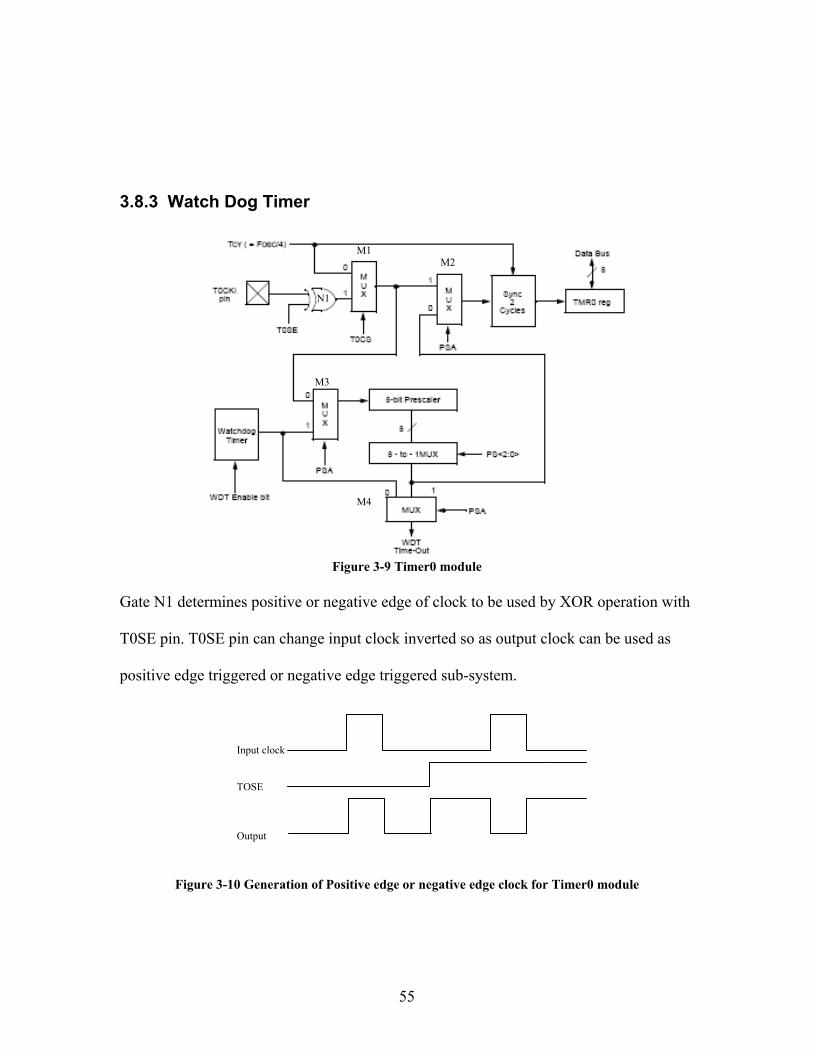
57
Figure 3-11 Generation of ramwr signal by MOVF instruction.
Figure 3-12 Skipping the count of present instruction from zero result
58
Similarly ZDout pin goes high when result is zero from execution of present
instruction. When INCFSZ or DECFSZ instruction is executed, ZDen pin high indicates
that present operation is zero for zero detection. A GOTO pin high enables 9 bit literal
from instruction set to be input to the program counter. At first by positive edge of clk1
PC+1 is pushed to the stack level 1 by positive edge of clk1 when clk2 is in negative
edge.
A rotate_en pin high selects operation of rotate left though carry (RLF) or rotate
right through carry (RRF). This operation involves rotating through left or right by rf pin.
rf pin set indicates that the operation involves rotate through left and rf low indicates that
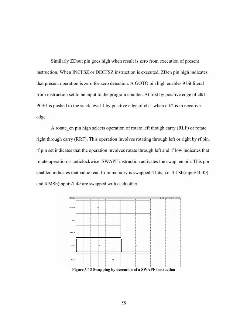
rotate operation is anticlockwise. SWAPF instruction activates the swap_en pin. This pin
enabled indicates that value read from memory is swapped 4 bits, i.e. 4 LSb(input<3:0>)
and 4 MSb(input<7:4> are swapped with each other.
Figure 3-13 Swapping by execution of a SWAPF instruction
59
A NOP instruction is a no operation instruction that generates the clock cycle, but
state of the machine is not altered. Only the program counter is incremented by one for
execution of the next instruction.
Arithmetic operations ADDWF, DECF, DECFSZ, INCF, INCFSZ and SUBWF
are all executed with arithmetic unit. This unit is activated by selection of active low
sel_fa pin. Logical operations involving ORing two operands, IORLW and IORWF are
activated by active low sel_or bit. Similarly, logical and operation ANDLW, ANDWF
are activated by active low sel_and bit. XORLW, XORWF signals activate active low
sel_xor operation. This generation is same as generation of sum signal without the carry
chain. So generation of sel_xor pin de-activates the carry chain, as XORed operation of
two inputs is processed. MOVLW, MOVF and MOVWF instructions involve in OR
operation with 00H. The result of ORing with input is always the same, i.e. the same bit
is passed through the operation and the status register can be latched. For an exception,
MOVWF instruction has no memory involved, so during write cycle, the ramwr signal is
activated and contents of accumulator were written to memory by write-back pin high.
CLRF and CLRW instructions read content from SRAM or accumulator and AND them
with zeroes.
Bit clear of memory (BCF) and Bit Set of memory (BSF) both involved a little bit
complex architecture. First 5 LSb were used as address to read contents from memory.
60
Now, remaining three bits 7, 6, and 5 are used to target one of eight bits. This is a general
case of 3 to 8 decoder. The zero on respective bit is set depending on address generated
by 3 to 8 decoder. For example, a 010b sets third bit low and rest to a high (11111011b,
FBh). Also BTFSZ and BTFSS instructions required operation of with a 8 to 1
multiplexer. Testing bit position was set by bits 7-5 in instruction set,. These bits were
used as an address to decode one out of eight bits. Result of this operation BTout is used
for latching PC+1 or PC+2 instructions in the program counter.
Unconditional branching instruction, GOTO when activated, latches contents of
instruction set’s bits<8:0> to PC latch. Also, at the same time the PC+1 is latched to the
stack segment 1.
Literal operations, ANDLW, IORLW, MOVLW, RETLW, and XORLW were
implemented by passing eight bit of literal through b bus to ALU. An inv_a pin inverts all
incoming bits of ALU_A bus to ALU. A high on inv_a pin does XOR operation of
incoming bits with 1 so that the result is an inverted bit. This pin is used for subtraction
A enable_a pin is used as input to ALU for bus ALU_A which discards any data coming
to the input pin and sets it as a low. This pin is used if ALU operation involves MOVing
contents from/to memory. A RETLW instruction is implemented as a two cycle
instruction. First, value of eight bit is moved to accumulator and similarly stack is
activated and output of stack is ready for next instruction cycle, latched to the program
counter.

61
A OPTION instruction is activated by logic high on option_en pin. This pin high
latches content of accumulator to 6 bit wide option register in negative edge of clock
cycle. Similarly TRIS instruction latches contents of accumulator to the TRIS register.
Contents of TRIS and OPTION are also mapped to SRAM and latched to their respective
address locations. Also contents of OPTION and TRIS register are latched to SRAM
during their write operations. A CALL instruction activates the stack segment. Next
instruction to be executed is loaded to the stack. New instruction location to be addressed
is stored in PC. Pins GOTO and stacksel are active during this operation. Negative edge
of clk1 and stacksel load values of PC+1 to stack and negative clk2 activates GOTO pin
which enables address set by call to call a subroutine latched to PC.
62
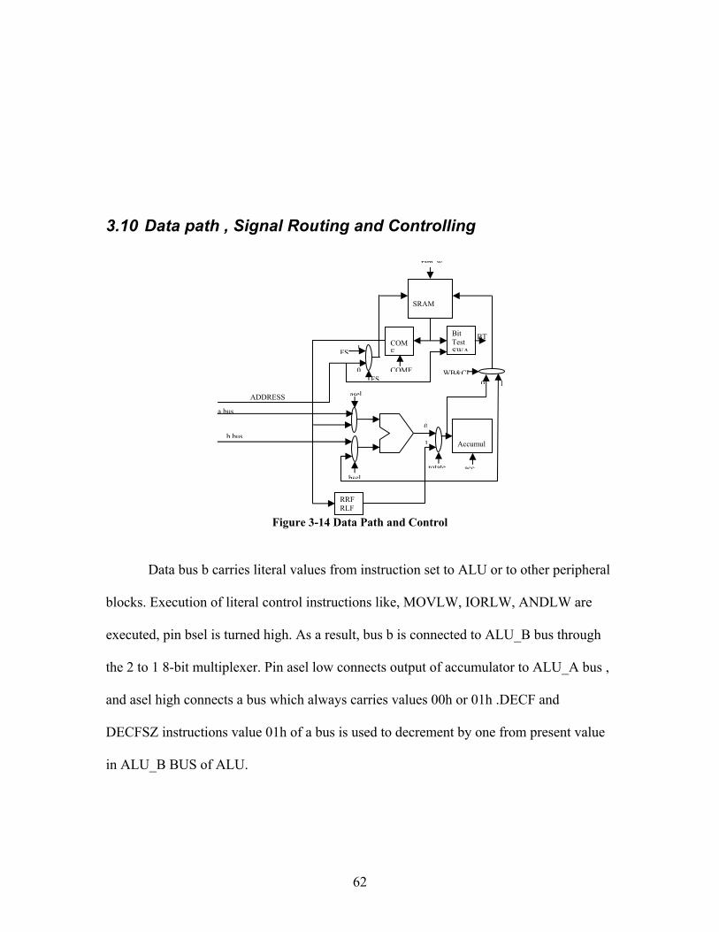
3.10 Data path , Signal Routing and Controlling
Figure 3-14 Data Path and Control
Data bus b carries literal values from instruction set to ALU or to other peripheral
blocks. Execution of literal control instructions like, MOVLW, IORLW, ANDLW are
executed, pin bsel is turned high. As a result, bus b is connected to ALU_B bus through
the 2 to 1 8-bit multiplexer. Pin asel low connects output of accumulator to ALU_A bus ,
and asel high connects a bus which always carries values 00h or 01h .DECF and
DECFSZ instructions value 01h of a bus is used to decrement by one from present value
in ALU_B BUS of ALU.
rotate acc
10WB&CL
ram w
FS
1
0
FS
0
1BT
bsel
asel
SRAM
COMF
RRF RLF
Bit Test SWA
Accumul
COMF
ADDRESS
a bus
b bus
63
Figure 3-15 asel and bsel controlling datapath to ALU
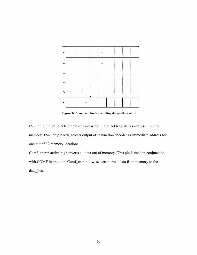
FSR_en pin high selects output of 5-bit wide File select Register as address input to
memory. FSR_en pin low, selects output of instruction decoder as immediate address for
one out of 32 memory locations.
Comf_en pin active high inverts all data out of memory. This pin is used in conjunction
with COMF instruction. Comf_en pin low, selects normal data from memory to the
data_bus.
64
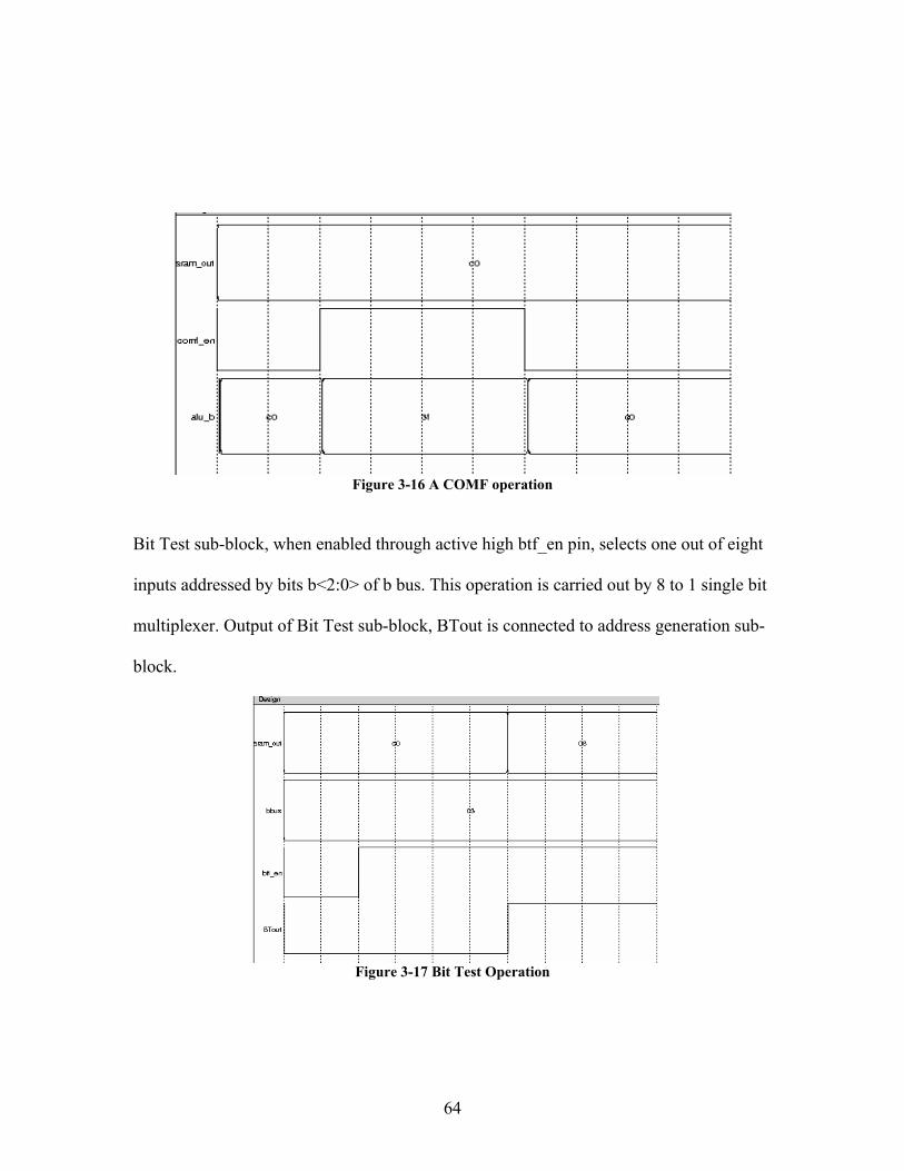
Figure 3-16 A COMF operation
Bit Test sub-block, when enabled through active high btf_en pin, selects one out of eight
inputs addressed by bits b<2:0> of b bus. This operation is carried out by 8 to 1 single bit
multiplexer. Output of Bit Test sub-block, BTout is connected to address generation sub-
block.
Figure 3-17 Bit Test Operation
65
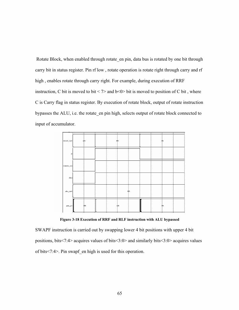
Rotate Block, when enabled through rotate_en pin, data bus is rotated by one bit through
carry bit in status register. Pin rf low , rotate operation is rotate right through carry and rf
high , enables rotate through carry right. For example, during execution of RRF
instruction, C bit is moved to bit < 7> and b<0> bit is moved to position of C bit , where
C is Carry flag in status register. By execution of rotate block, output of rotate instruction
bypasses the ALU, i.e. the rotate_en pin high, selects output of rotate block connected to
input of accumulator.
Figure 3-18 Execution of RRF and RLF instruction with ALU bypassed SWAPF instruction is carried out by swapping lower 4 bit positions with upper 4 bit
positions, bits<7:4> acquires values of bits<3:0> and similarly bits<3:0> acquires values
of bits<7:4>. Pin swapf_en high is used for this operation.
66
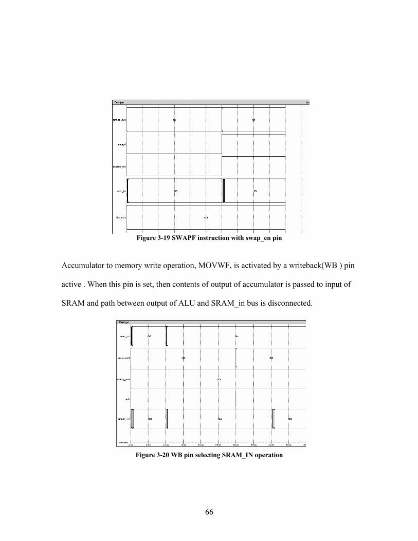
Figure 3-19 SWAPF instruction with swap_en pin
Accumulator to memory write operation, MOVWF, is activated by a writeback(WB ) pin
active . When this pin is set, then contents of output of accumulator is passed to input of
SRAM and path between output of ALU and SRAM_in bus is disconnected.
Figure 3-20 WB pin selecting SRAM_IN operation
67
3.11 Status Register
5-bit status register is clocked individually on each bit positions. C (carry) is activated
with rotate_en and add_subwf both high and during negative edge of clk2. Digit Carry
(DC) , bit position b<1> is activated only on negative edge of clk2 and high add_subwf
instruction. Zero bit (Z), b<2> is activated by negative edge of clk2 and ZDen bit active
high. Power Down ( PD ) ,b<3> is activated only by active high CLRWDT and SLEEP
on negative edge of clk2. Similarly Time Out (TO) bit<4> is activated on time out on
Watch Dog Timer.
68
Chapter 4
4 Instruction Execution This chapter explains execution of all 33 instructions in detail. Here instructions are
classified as
• Byte oriented
• Bit oriented
• Literal and Control
In the following examples presented, all tests were carried out on IRSIM simulator. In
some instructions d represents the destination bit, fffff represent five bit address input to
memory location, and bbb represent 3-bit bit locator. Section 2.19 explains instruction
format in detail.
4.1 Byte Oriented Instructions
4.1.1 ADDWF
General operation of ADDWF involves adding contents of accumulator and memory .
Result is placed either in accumulator or memory depending on instruction bit<5>.
Encoding format: 0001 11df ffff
Description To verify operation of this instruction, two instructions are used, 1C0h ( for
writing to accumulator) and 1E0h ( for writing to memory). In execution of 1C0h
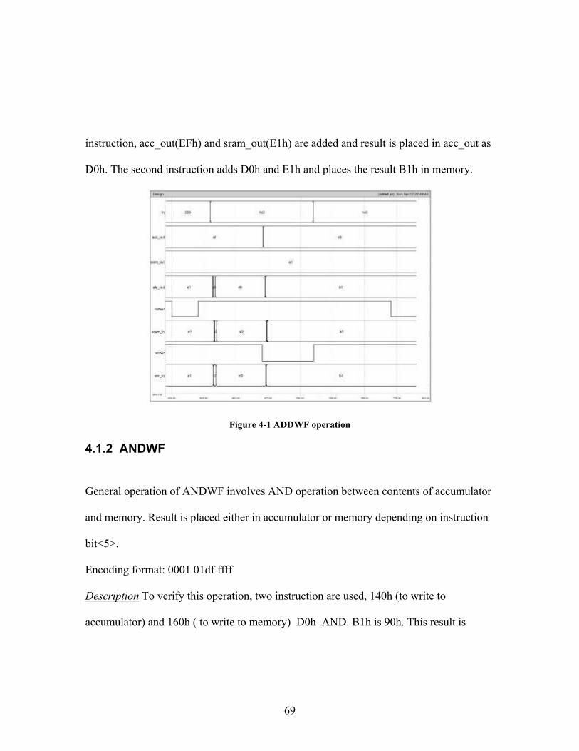
69
instruction, acc_out(EFh) and sram_out(E1h) are added and result is placed in acc_out as
D0h. The second instruction adds D0h and E1h and places the result B1h in memory.
Figure 4-1 ADDWF operation
4.1.2 ANDWF
General operation of ANDWF involves AND operation between contents of accumulator
and memory. Result is placed either in accumulator or memory depending on instruction
bit<5>.
Encoding format: 0001 01df ffff
Description To verify this operation, two instruction are used, 140h (to write to
accumulator) and 160h ( to write to memory) D0h .AND. B1h is 90h. This result is
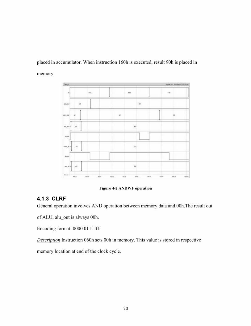
70
placed in accumulator. When instruction 160h is executed, result 90h is placed in
memory.
Figure 4-2 ANDWF operation
4.1.3 CLRF General operation involves AND operation between memory data and 00h.The result out
of ALU, alu_out is always 00h.
Encoding format: 0000 011f ffff
Description Instruction 060h sets 00h in memory. This value is stored in respective
memory location at end of the clock cycle.
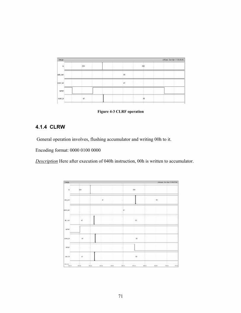
71
Figure 4-3 CLRF operation
4.1.4 CLRW General operation involves, flushing accumulator and writing 00h to it.
Encoding format: 0000 0100 0000
Description Here after execution of 040h instruction, 00h is written to accumulator.
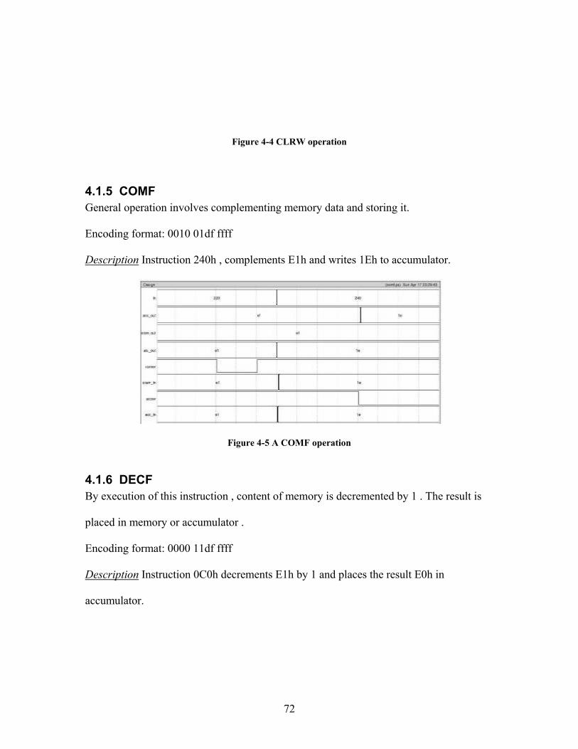
72
Figure 4-4 CLRW operation
4.1.5 COMF General operation involves complementing memory data and storing it.
Encoding format: 0010 01df ffff
Description Instruction 240h , complements E1h and writes 1Eh to accumulator.
Figure 4-5 A COMF operation
4.1.6 DECF By execution of this instruction , content of memory is decremented by 1 . The result is
placed in memory or accumulator .
Encoding format: 0000 11df ffff
Description Instruction 0C0h decrements E1h by 1 and places the result E0h in
accumulator.
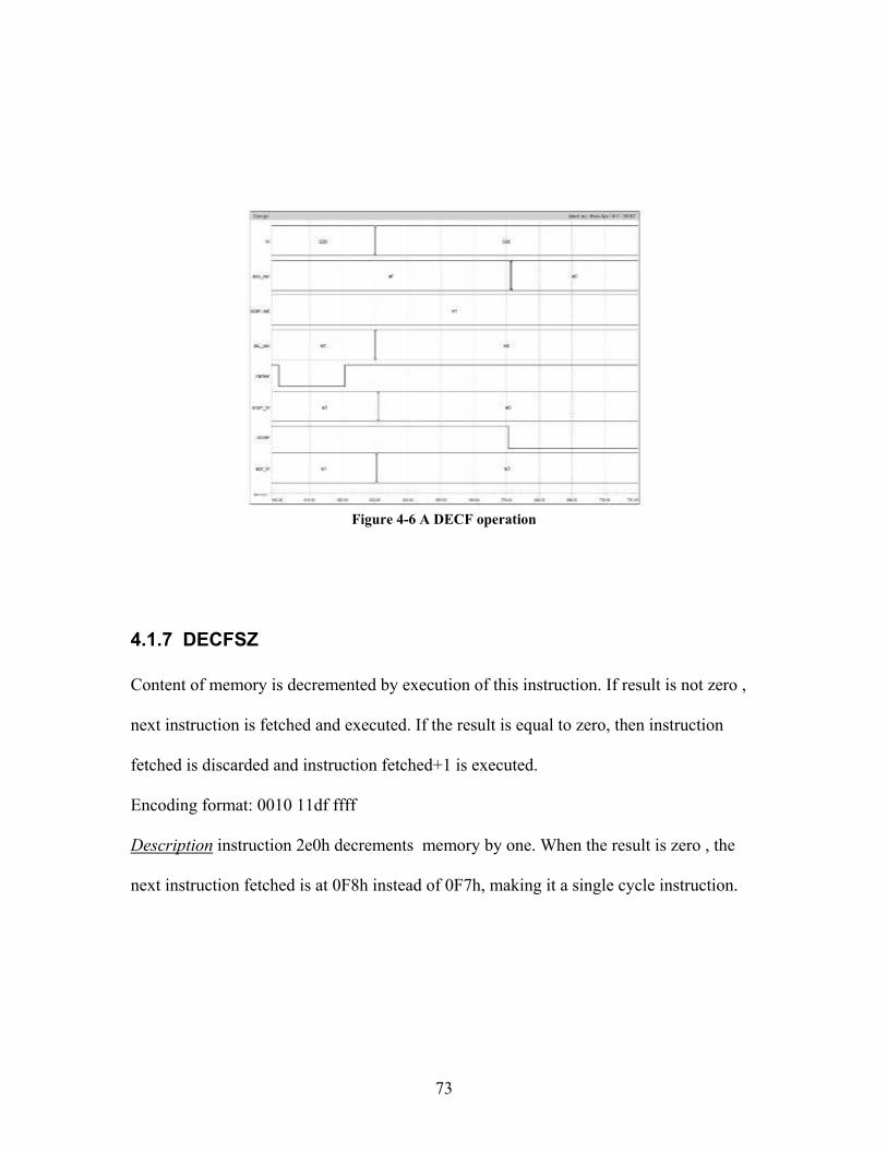
73
Figure 4-6 A DECF operation
4.1.7 DECFSZ Content of memory is decremented by execution of this instruction. If result is not zero ,
next instruction is fetched and executed. If the result is equal to zero, then instruction
fetched is discarded and instruction fetched+1 is executed.
Encoding format: 0010 11df ffff
Description instruction 2e0h decrements memory by one. When the result is zero , the
next instruction fetched is at 0F8h instead of 0F7h, making it a single cycle instruction.

74
Figure 4-7 DECFSZ operation
4.1.8 INCF
Content of memory is incremented by one. Result is placed in accumulator or memory
depending on the instruction bit<5>.
Encoding format: 0010 10df ffff
Description By execution of instruction 220h, E1h (output of memory) is incremented by
one, and written back to memory.
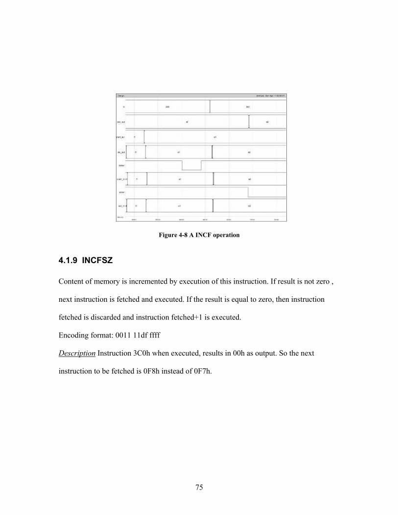
75
Figure 4-8 A INCF operation
4.1.9 INCFSZ
Content of memory is incremented by execution of this instruction. If result is not zero ,
next instruction is fetched and executed. If the result is equal to zero, then instruction
fetched is discarded and instruction fetched+1 is executed.
Encoding format: 0011 11df ffff
Description Instruction 3C0h when executed, results in 00h as output. So the next
instruction to be fetched is 0F8h instead of 0F7h.
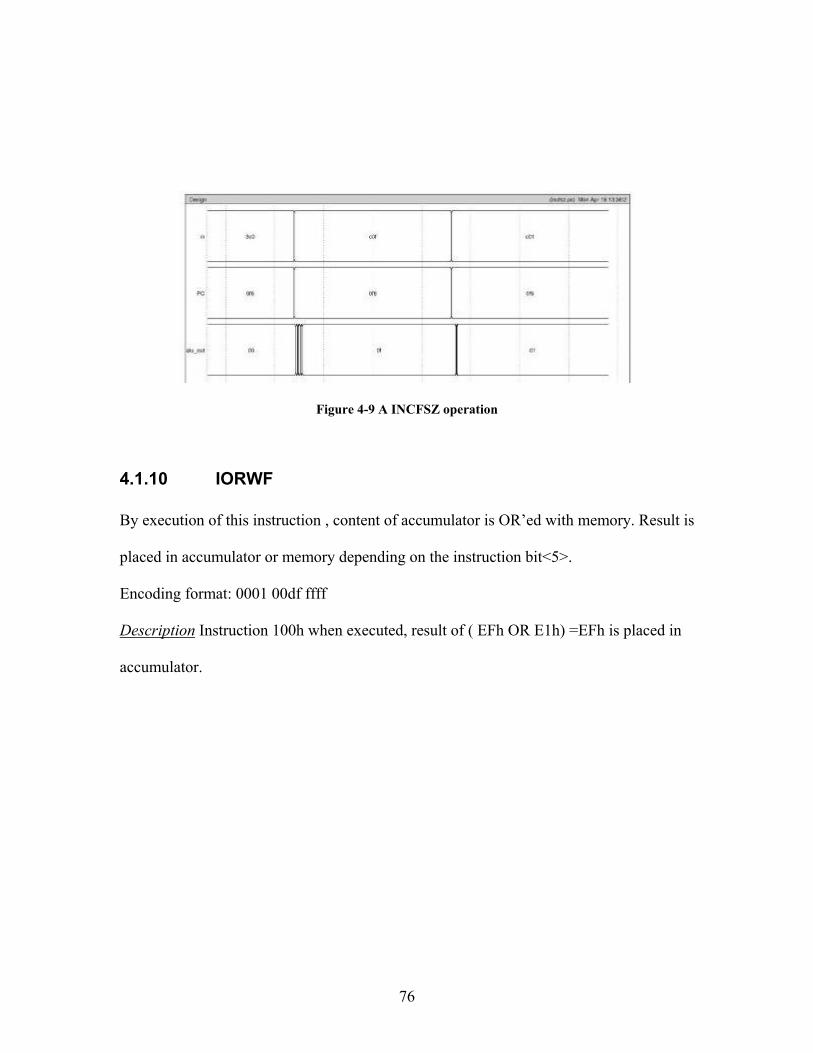
76
Figure 4-9 A INCFSZ operation
4.1.10 IORWF By execution of this instruction , content of accumulator is OR’ed with memory. Result is
placed in accumulator or memory depending on the instruction bit<5>.
Encoding format: 0001 00df ffff
Description Instruction 100h when executed, result of ( EFh OR E1h) =EFh is placed in
accumulator.
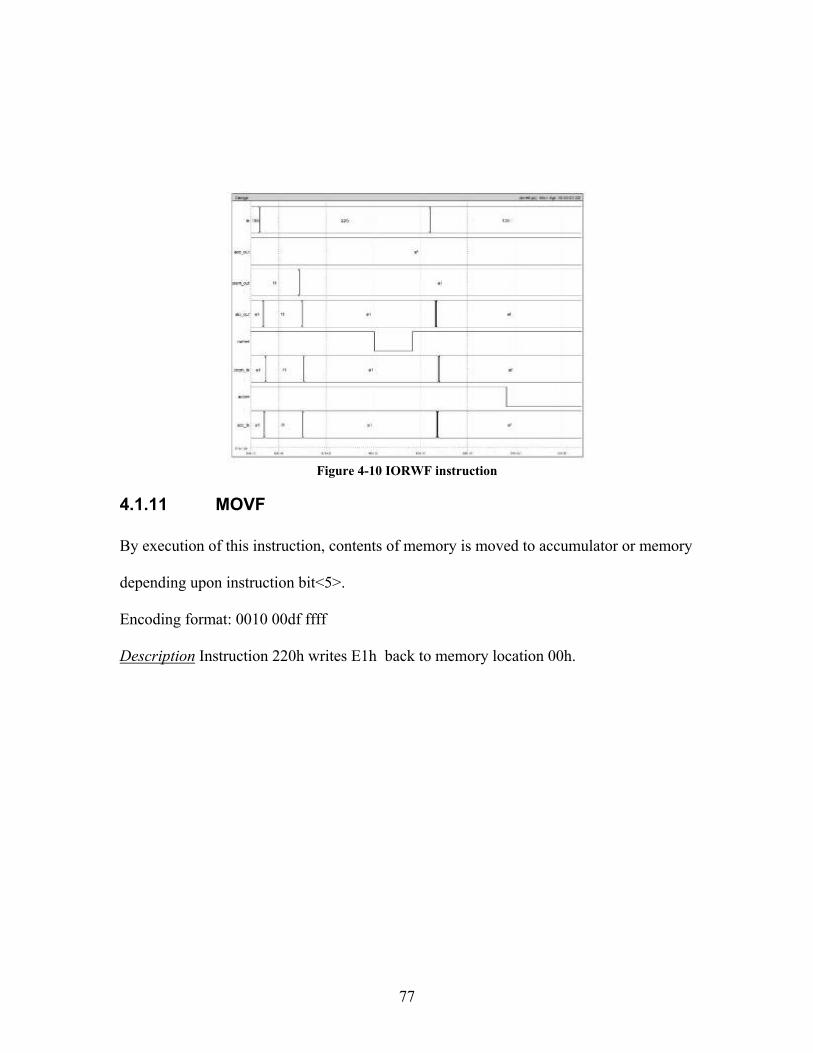
77
Figure 4-10 IORWF instruction
4.1.11 MOVF By execution of this instruction, contents of memory is moved to accumulator or memory
depending upon instruction bit<5>.
Encoding format: 0010 00df ffff
Description Instruction 220h writes E1h back to memory location 00h.
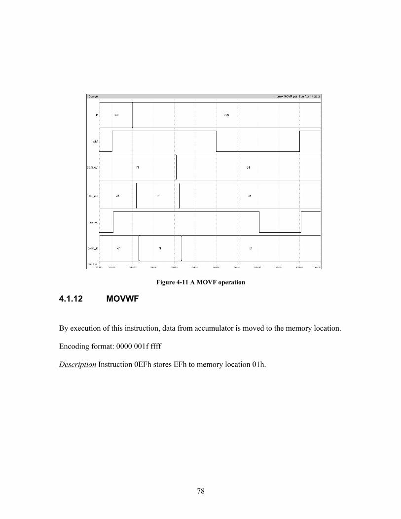
78
Figure 4-11 A MOVF operation
4.1.12 MOVWF
By execution of this instruction, data from accumulator is moved to the memory location.
Encoding format: 0000 001f ffff
Description Instruction 0EFh stores EFh to memory location 01h.
79
4.1.13 NOP As the name implies, no operation is done, by execution of this instruction.
Encoding format: 0000 0000 0000
Description Instruction 000h when executed, changes nothing and no control signals are
generated.
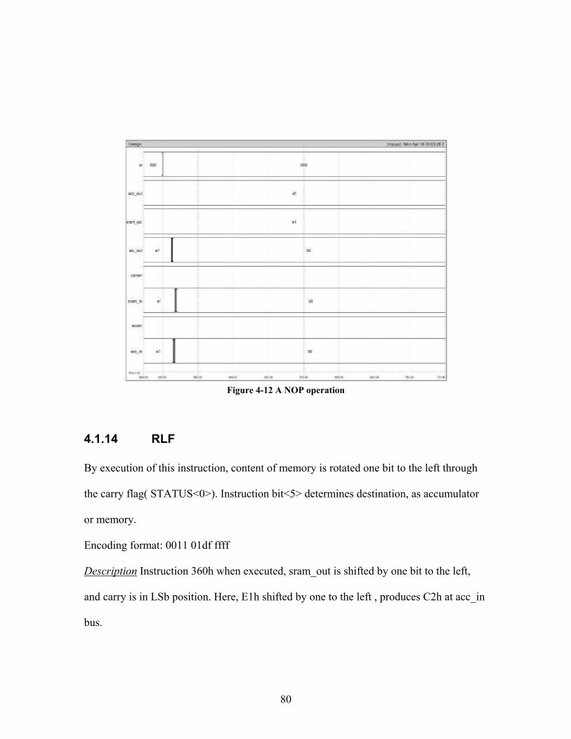
80
Figure 4-12 A NOP operation
4.1.14 RLF By execution of this instruction, content of memory is rotated one bit to the left through
the carry flag( STATUS<0>). Instruction bit<5> determines destination, as accumulator
or memory.
Encoding format: 0011 01df ffff
Description Instruction 360h when executed, sram_out is shifted by one bit to the left,
and carry is in LSb position. Here, E1h shifted by one to the left , produces C2h at acc_in
bus.
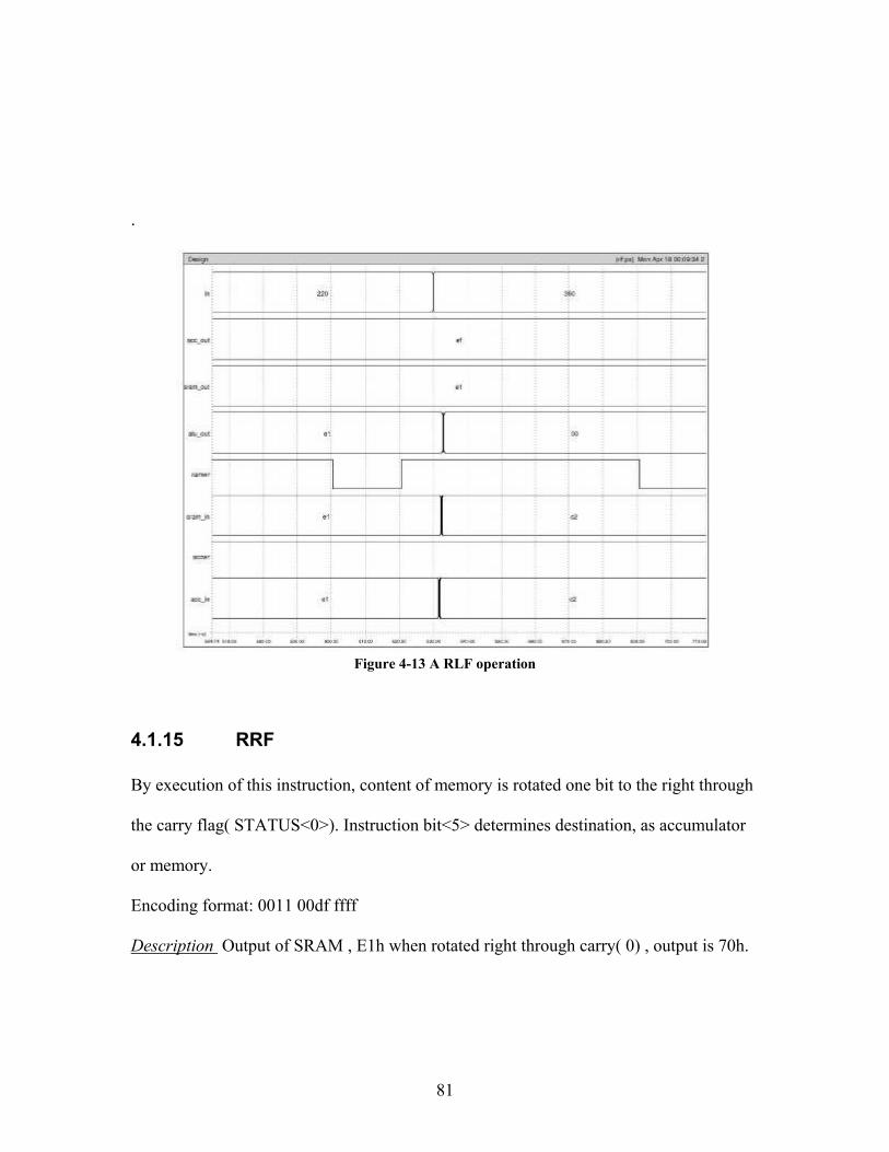
81
.
Figure 4-13 A RLF operation
4.1.15 RRF By execution of this instruction, content of memory is rotated one bit to the right through
the carry flag( STATUS<0>). Instruction bit<5> determines destination, as accumulator
or memory.
Encoding format: 0011 00df ffff
Description Output of SRAM , E1h when rotated right through carry( 0) , output is 70h.
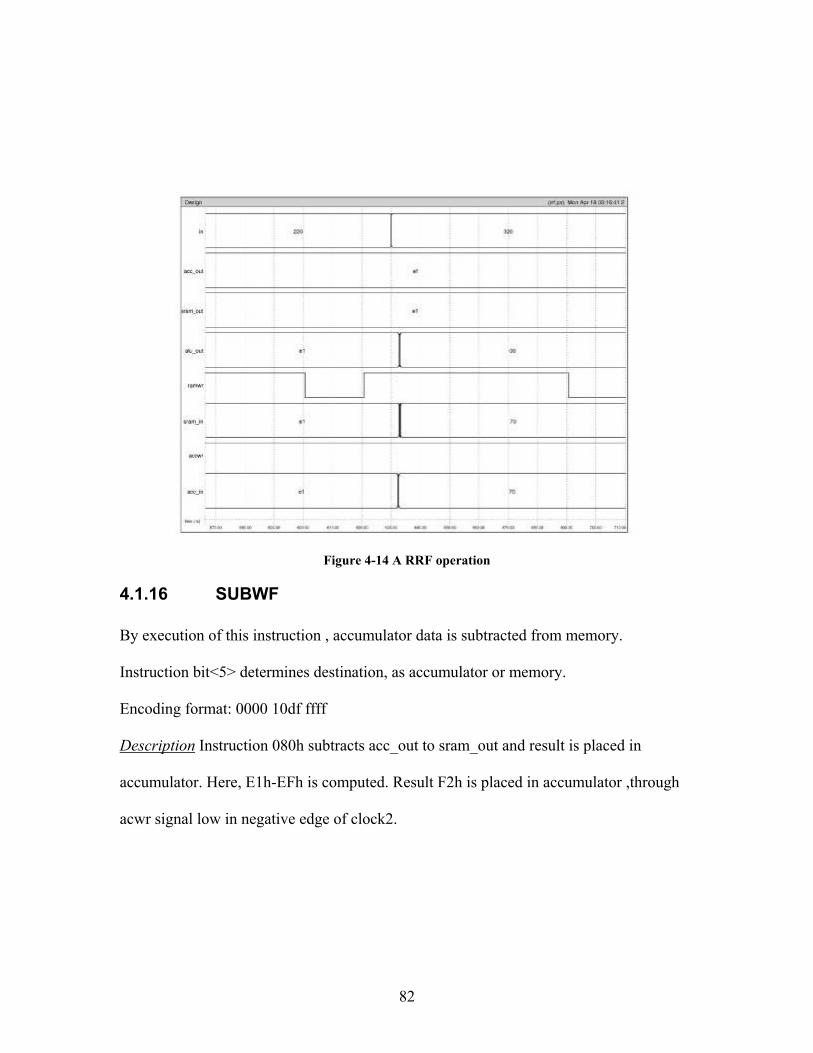
82
Figure 4-14 A RRF operation
4.1.16 SUBWF By execution of this instruction , accumulator data is subtracted from memory.
Instruction bit<5> determines destination, as accumulator or memory.
Encoding format: 0000 10df ffff
Description Instruction 080h subtracts acc_out to sram_out and result is placed in
accumulator. Here, E1h-EFh is computed. Result F2h is placed in accumulator ,through
acwr signal low in negative edge of clock2.
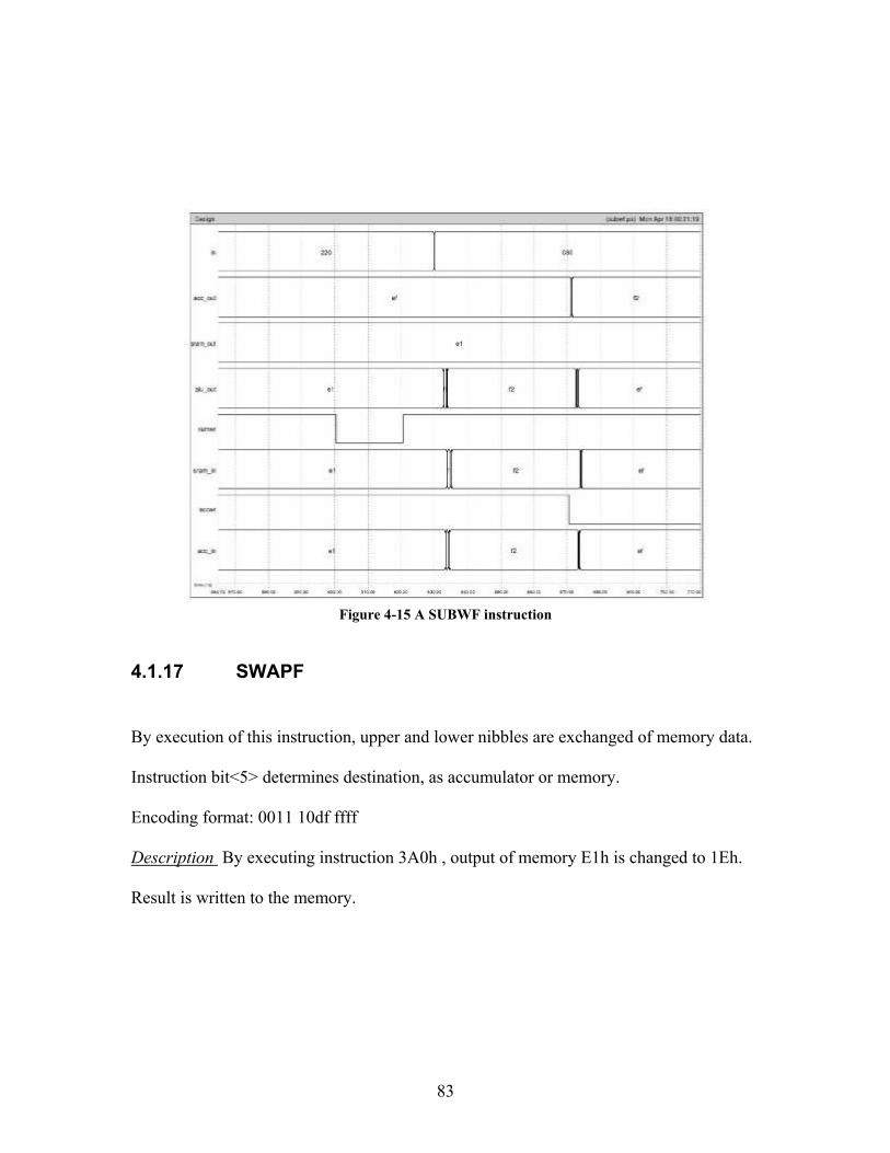
83
Figure 4-15 A SUBWF instruction
4.1.17 SWAPF
By execution of this instruction, upper and lower nibbles are exchanged of memory data.
Instruction bit<5> determines destination, as accumulator or memory.
Encoding format: 0011 10df ffff
Description By executing instruction 3A0h , output of memory E1h is changed to 1Eh.
Result is written to the memory.

84
Figure 4-16 A SWAPF instruction
4.1.18 XORWF By execution of this instruction , contents of accumulator and memory are exclusive
ORed. Instruction bit<5> determines destination, as accumulator or memory.
Encoding format: 0001 10df ffff
Description Instruction 1A0h performs an XOR operation between accumulator and
memory data, and result is written in memory. Here result 0Eh ( EFh XOR E1h) is
written to memory.
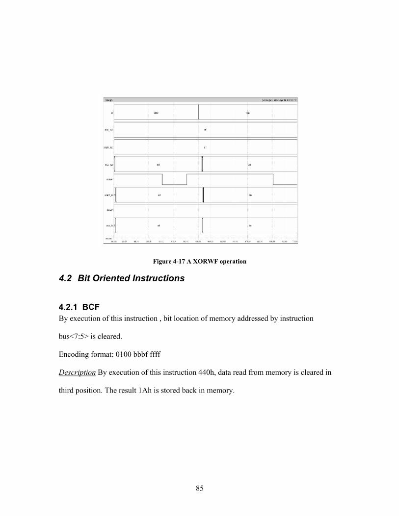
85
Figure 4-17 A XORWF operation
4.2 Bit Oriented Instructions
4.2.1 BCF By execution of this instruction , bit location of memory addressed by instruction
bus<7:5> is cleared.
Encoding format: 0100 bbbf ffff
Description By execution of this instruction 440h, data read from memory is cleared in
third position. The result 1Ah is stored back in memory.
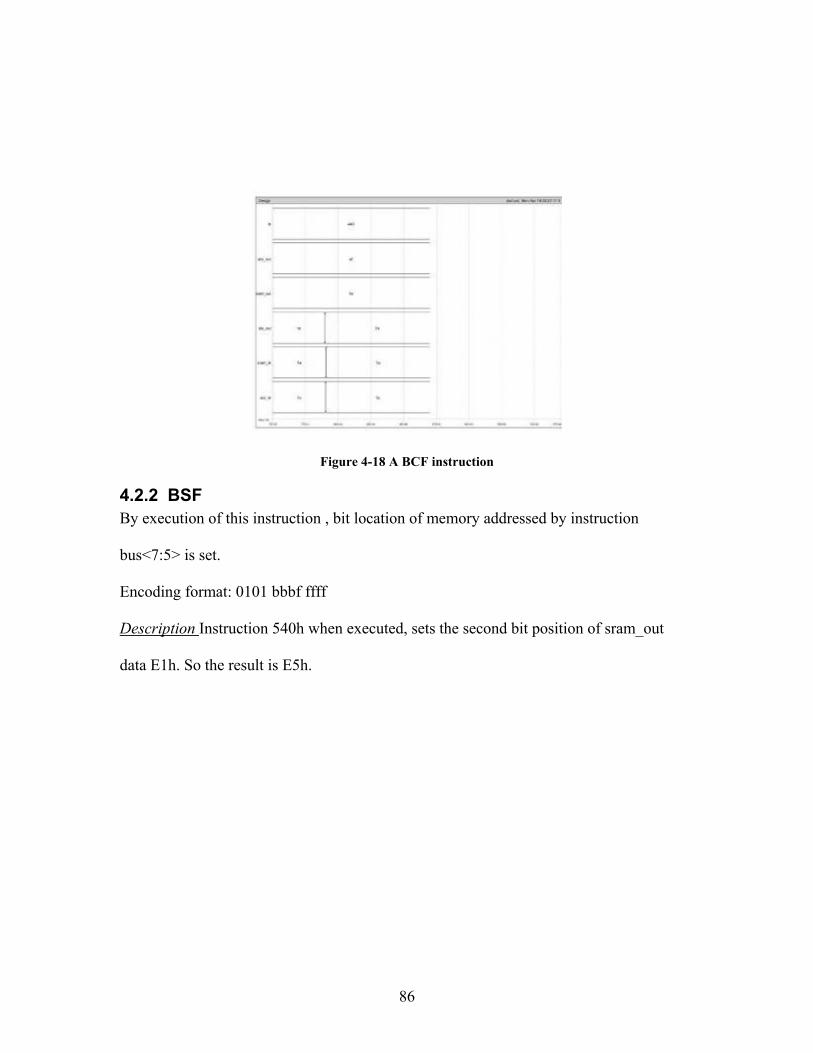
86
Figure 4-18 A BCF instruction
4.2.2 BSF By execution of this instruction , bit location of memory addressed by instruction
bus<7:5> is set.
Encoding format: 0101 bbbf ffff
Description Instruction 540h when executed, sets the second bit position of sram_out
data E1h. So the result is E5h.
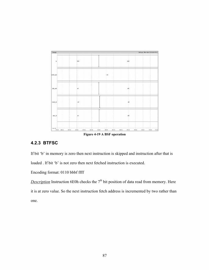
87
Figure 4-19 A BSF operation
4.2.3 BTFSC If bit ‘b’ in memory is zero then next instruction is skipped and instruction after that is
loaded . If bit ‘b’ is not zero then next fetched instruction is executed.
Encoding format: 0110 bbbf ffff
Description Instruction 6E0h checks the 7th bit position of data read from memory. Here
it is at zero value. So the next instruction fetch address is incremented by two rather than
one.

88
Figure 4-20 A BTFSC operation
4.2.4 BTFSS If bit ‘b’ in memory is one, then next instruction is skipped and instruction after that is
loaded . If bit ‘b’ is not one then next fetched instruction is executed.
Encoding format: 0110 bbbf ffff
Description Instruction 7E0h checks the 7th bit of output of memory. Here, this bit is at
logic 1, so the instruction , C0Fh is fetched from PC+2, i.e. 0F8h memory location.
Figure 4-21 A BTFSS operation
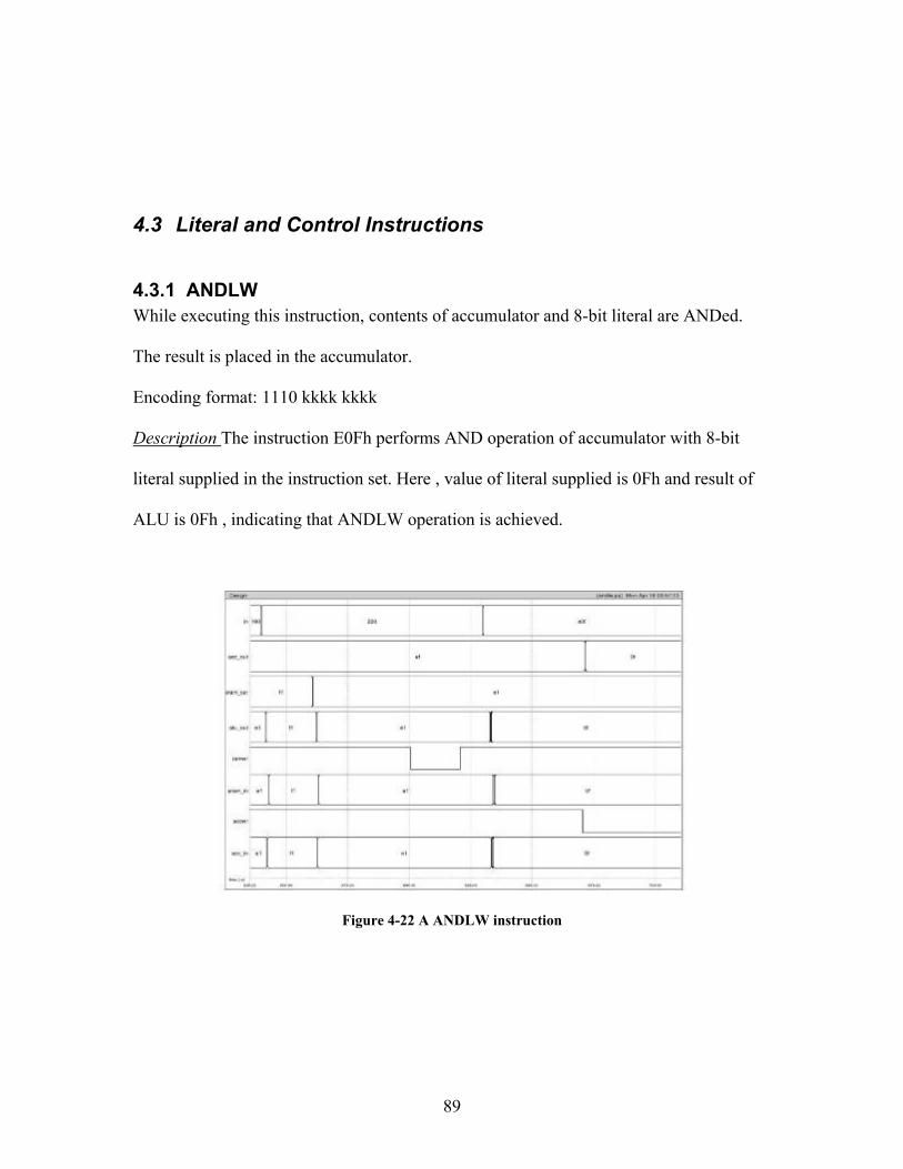
89
4.3 Literal and Control Instructions
4.3.1 ANDLW While executing this instruction, contents of accumulator and 8-bit literal are ANDed.
The result is placed in the accumulator.
Encoding format: 1110 kkkk kkkk
Description The instruction E0Fh performs AND operation of accumulator with 8-bit
literal supplied in the instruction set. Here , value of literal supplied is 0Fh and result of
ALU is 0Fh , indicating that ANDLW operation is achieved.
Figure 4-22 A ANDLW instruction

90
4.3.2 IORLW While executing this instruction, contents of accumulator are ORed with 8-bit literal
value. Result is placed in the accumulator.
Encoding format: 1101 kkkk kkkk
Description 8-bit literal 0Fh is ORed with accumulator output (0Fh). The result 0Fh is
placed in accumulator register.
Figure 4-23 A IORLW instruction
4.3.3 MOVLW The 8-bit literal is loaded to the accumulator after execution of this instruction.
Encoding format: 1100 kkkk kkkk
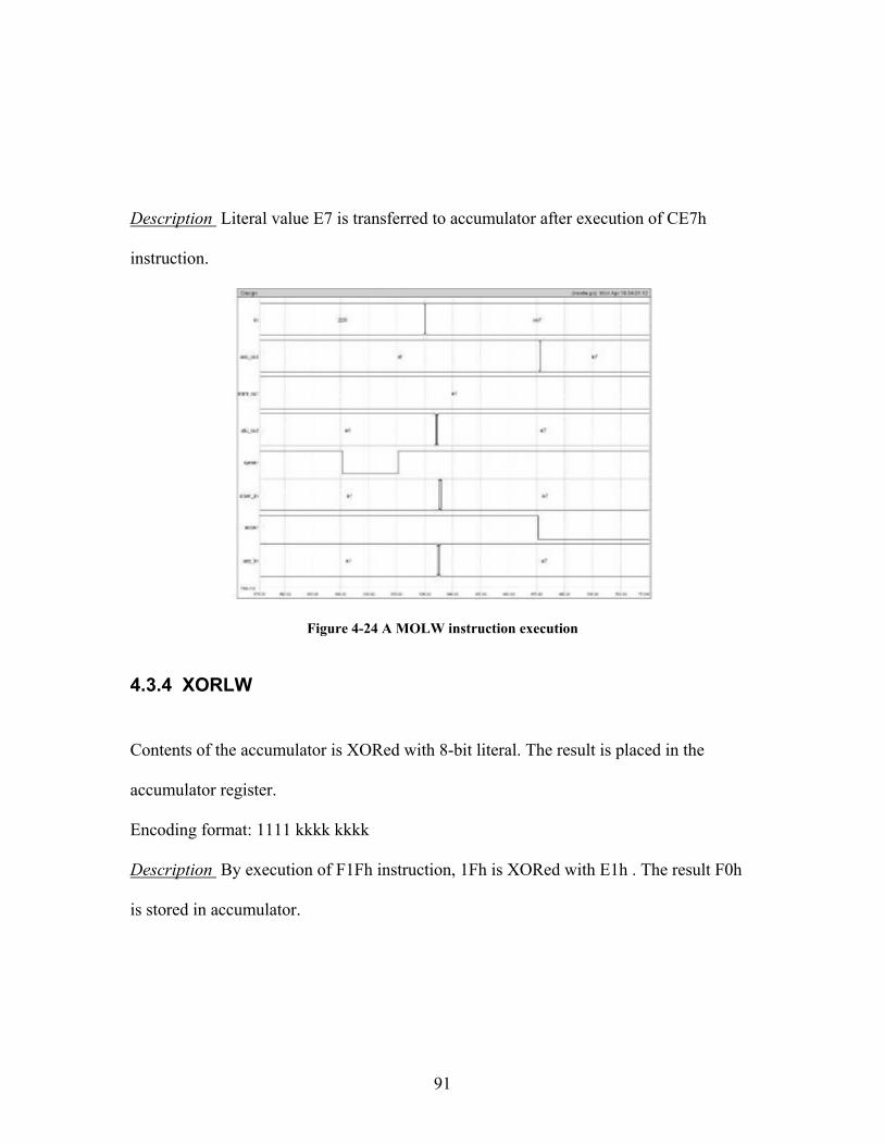
91
Description Literal value E7 is transferred to accumulator after execution of CE7h
instruction.
Figure 4-24 A MOLW instruction execution
4.3.4 XORLW
Contents of the accumulator is XORed with 8-bit literal. The result is placed in the
accumulator register.
Encoding format: 1111 kkkk kkkk
Description By execution of F1Fh instruction, 1Fh is XORed with E1h . The result F0h
is stored in accumulator.
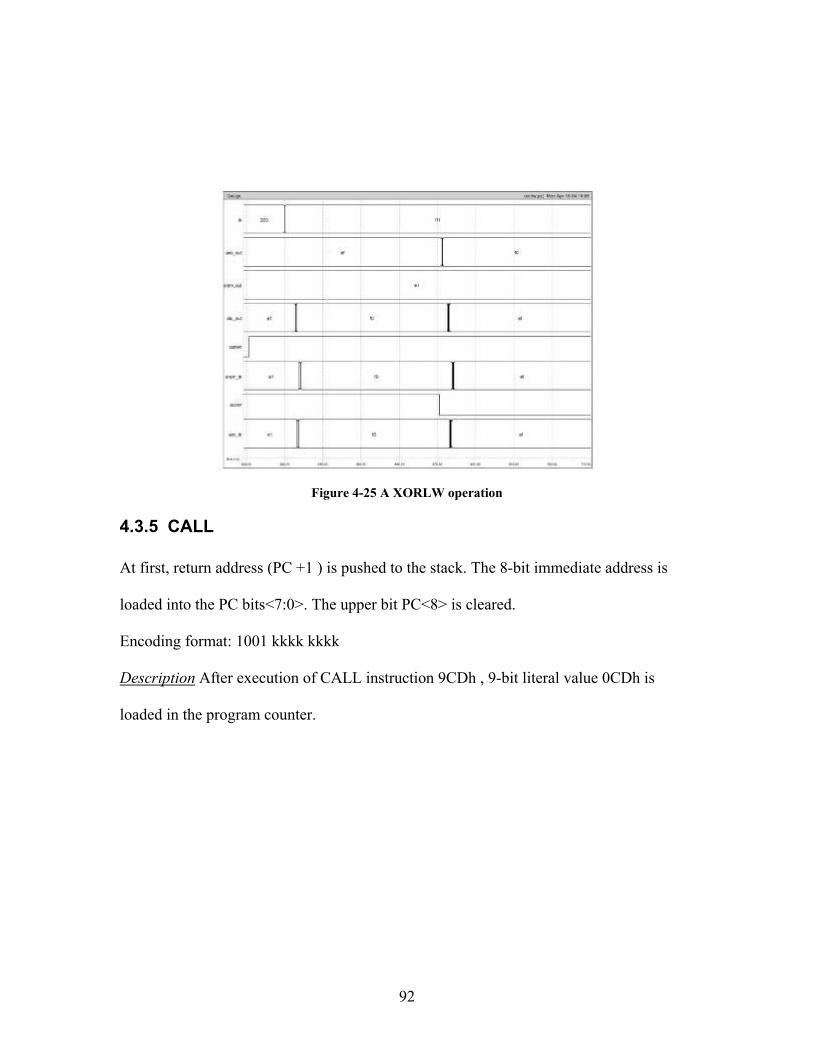
92
Figure 4-25 A XORLW operation
4.3.5 CALL At first, return address (PC +1 ) is pushed to the stack. The 8-bit immediate address is
loaded into the PC bits<7:0>. The upper bit PC<8> is cleared.
Encoding format: 1001 kkkk kkkk
Description After execution of CALL instruction 9CDh , 9-bit literal value 0CDh is
loaded in the program counter.
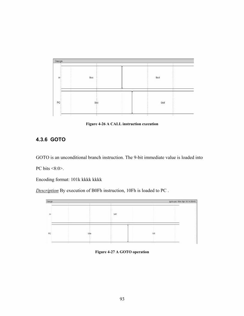
93
Figure 4-26 A CALL instruction execution
4.3.6 GOTO
GOTO is an unconditional branch instruction. The 9-bit immediate value is loaded into
PC bits <8:0>.
Encoding format: 101k kkkk kkkk
Description By execution of B0Fh instruction, 10Fh is loaded to PC .
Figure 4-27 A GOTO operation

94
4.3.7 TRIS
After execution of this instruction , TRIS register is loaded with contents of accumulator
register.
Encoding format: 0000 0000 0fff
Description Here instruction 006h loads contents of accumulator F2h to the TRISB
register.
Figure 4-28 A TRIS operation

95
5 Conclusion and Future Work The project was a success both in terms of what I have learned and what I have
accomplished.
This project reinforced many important VLSI concepts. One aspect of VLSI which I
became very familiar was the idea of trade-offs. AT different itmes, there was limitation
in choosing increased area or increased speed. In many cases, layout of intracell was
limited to metal1 and metal2. This increased overall area by a little, but in other hand
speed was increased subsequently. All over our design, routing via poly was minimized
as possible.
There were many other VLSI concepts which I learned from working on this project. I
learned to design circuits, for replication. Also ,I learned floor planning, channel routing,
and designing at lower level to accommodate top level floor planning and routing.
Lot of time, I encountered problem while simulating the design. Simple combinational
logic created no problem while simulation . Higher level design connecting multiple pins
and control signals was troublesome to some extent. To count a few, I had problem for a
long time on test bench for tristate buffers and static memories. For a tristate buffer, I was

96
on right track, but it took a week for me to figure that out. Similarly , D-latch also
aroused a lot of problem for me . I tried each and every design patterns but was not able
to analyze the test result and figure out that I was headed the right direction. Static RAM
was one of the most troublesome while designing. Reading and writing though was
perfectly achieved on a single cell, I had a lot of problem on Memory array. It would not
store anything at all. After many days, I figured out that the word lines was enabled a
long time before pre-charge went high( active low signal). This was creating a big mess.
Also , channel routing and final assembly was creating a havoc by not connecting 12
metal1 to metal2 data paths. It made me to rewire everything thrice. But thanks to the
problem, which made me to rethink about floor planning and everything next was
perfectly organized and compact.
Test benches written on spectre as too much of work. I wanted a fast and simple
alternative. Two simulators, spectreS and IRSIM were used. IRSIM was used for large IO
pins and for smaller pins spectreS was used.
Moreover , I gained a lot from this work . I was really happy to see my design working
faster and performing all the 33 instructions pretty fast.
Finally , I would like to conclude this project as a 8-bit microcontroller operating with a
total access time of 14nS
97
5.1 Future Work • Timing analysis
Detailed timing analysis is yet to be done on this project. Doing so , performance
of the machine can be increased.
• Instruction memory is yet to be designed.
• Adding RS232 serial interface.
• Pipelining the whole design
At this phase of project, the whole design is only pipelined by two stages.
The first phase is fetch and the second is decode. If this whole system is pipelined to 4
different stages, then a faster performance can be achieved.
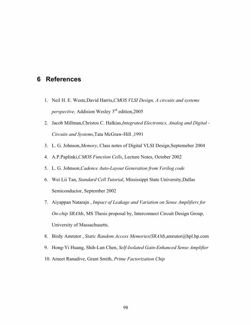
98
6 References
1. Neil H. E. Weste,David Harris,CMOS VLSI Design, A circuits and systems
perspective, Addision Wesley 3rd edition,2005
2. Jacob Millman,Christos C. Halkias,Integrated Electronics, Analog and Digital -
Circuits and Systems,Tata McGraw-Hill ,1991
3. L. G. Johnson,Memory, Class notes of Digital VLSI Design,Septemeber 2004
4. A.P.Paplinki,CMOS Function Cells, Lecture Notes, October 2002
5. L. G. Johnson,Cadence Auto-Layout Generation from Verilog code
6. Wei Lii Tan, Standard Cell Tutorial, Mississippi State University,Dallas
Semiconductor, September 2002
7. Aiyappan Natarajn , Impact of Leakage and Variation on Sense Amplifiers for
On-chip SRAMs, MS Thesis proposal by, Interconnect Circuit Design Group,
University of Massachusetts.
8. Birdy Amrutor , Static Random Access Memories(SRAM),[email protected]
9. Hong-Yi Huang, Shih-Lun Chen, Self-Isolated Gain-Enhanced Sense Amplifier
10. Ameet Ranadive, Grant Smith, Prime Factorization Chip

99
11. Dan Clein, What is Full Custom layout Design,
www.eetimes.com/isd/features/OEG20010608S0035
12. PIC microcontrollers,
http://www.mikroelektronika.co.yu/english/product/books/PICbook/
100
7 Bibliography
1. L. G. Johnson, Lecture notes on Digital VLSI Design
2. DS304538D: 8 bit EPROM/ROM based CMOS Microcontrollers, Microchip
Technologies Inc. 2002
3. Neil H. E. Westet, Kamran Eshraghian,Principles of CMOS VLSI Design, A
system perspective,2nd edition
4. Douglas V. Hall,Microprocessors and Interfacing,Programming andHardware
,Tata McGraw-Hill 1991
5. Barry B. Brey, The INTEL Microprocessors,
8086/8088,80186/80188,80286,80386,80486,Pentium and Pentium Pro
Processor. Architecture ,Programming and Interfacing,Prentice-Hall of India
1998
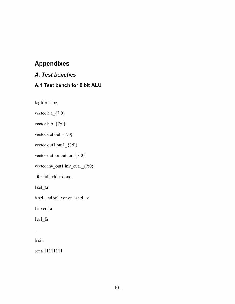
101
Appendixes
A. Test benches
A.1 Test bench for 8 bit ALU
logfile 1.log
vector a a_{7:0}
vector b b_{7:0}
vector out out_{7:0}
vector out1 out1_{7:0}
vector out_or out_or_{7:0}
vector inv_out1 inv_out1_{7:0}
| for full adder done ,
l sel_fa
h sel_and sel_xor en_a sel_or
l invert_a
l sel_fa
s
h cin
set a 11111111

102
set b 00000001
s
assert out 00000001
set a 00000000
set b 00000000
l cin
s
l cin
set a 10101010
set b 01010101
s
h cin
set a 11111110
set b 00000000
s
assert out 11111111
assert cout 0
set a 01000000
set b 00010000
s
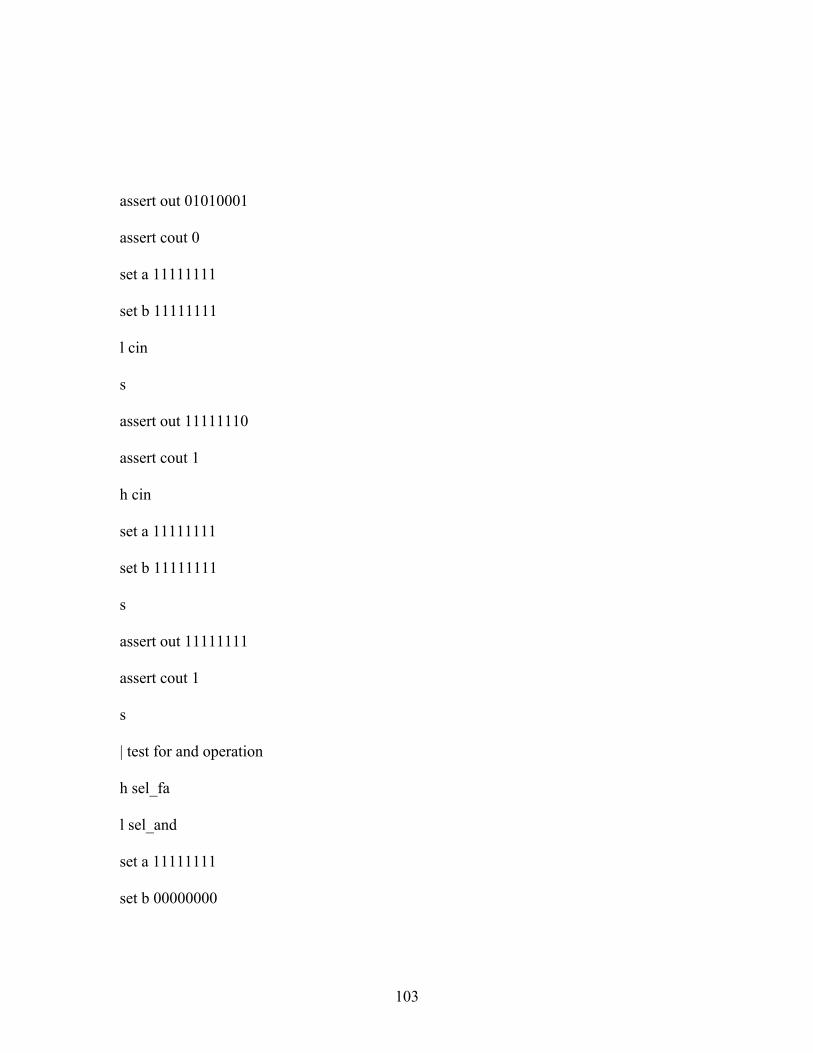
103
assert out 01010001
assert cout 0
set a 11111111
set b 11111111
l cin
s
assert out 11111110
assert cout 1
h cin
set a 11111111
set b 11111111
s
assert out 11111111
assert cout 1
s
| test for and operation
h sel_fa
l sel_and
set a 11111111
set b 00000000
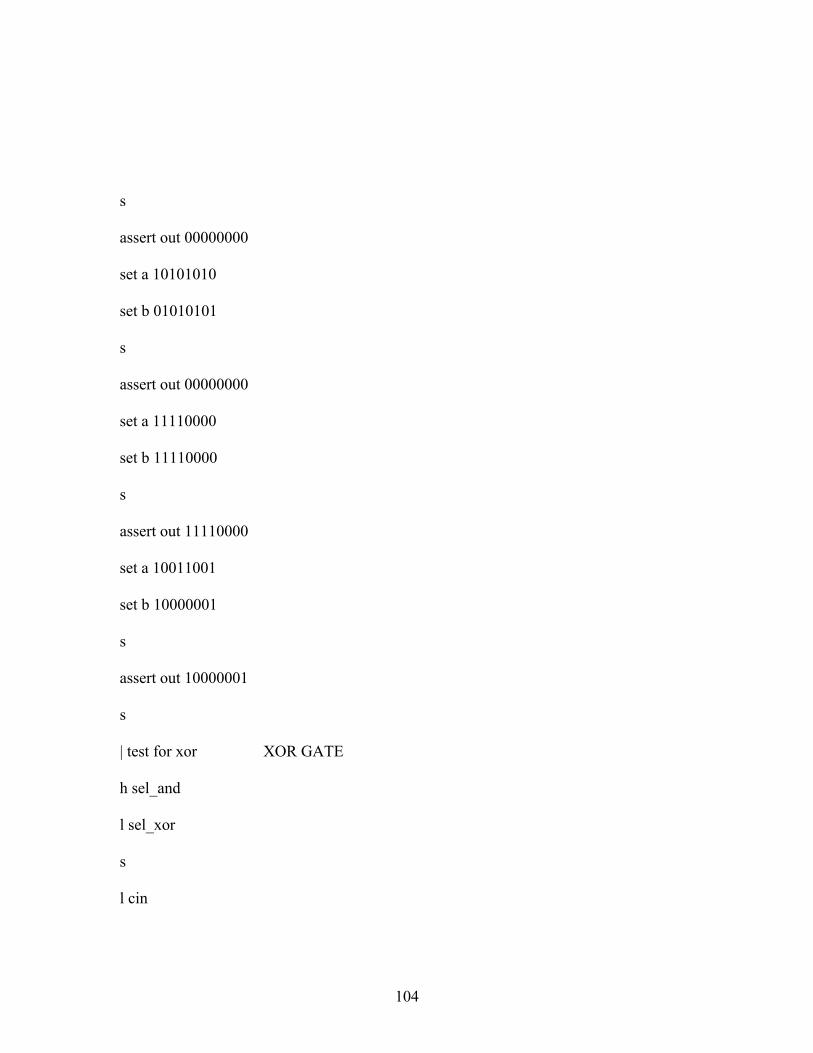
104
s
assert out 00000000
set a 10101010
set b 01010101
s
assert out 00000000
set a 11110000
set b 11110000
s
assert out 11110000
set a 10011001
set b 10000001
s
assert out 10000001
s
| test for xor XOR GATE
h sel_and
l sel_xor
s
l cin

105
set a 11111110
set b 10000001
s
assert out 01111111
set a 00000001
set b 10101010
s
assert out 10101011
| test for b-a SUBSTRACT
l sel_fa
h sel_xor
h cin
h invert_a
set b 11111111
set a 00000001
s
assert out 11111110
set b 00001010
set a 00000010

106
s
assert out 00001000
set b 00000001
set a 00000001
s
assert out 00000000
set b 00010001
set a 10000000
s
assert out 10010001
set b 00000000
set a 11111111
s
assert out 00000001
| test for B + 1 B+1
l en_a
h cin
l invert_a
set b 00000000
set a 11111111
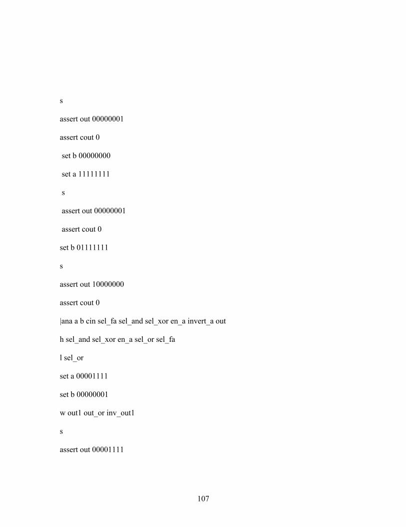
107
s
assert out 00000001
assert cout 0
set b 00000000
set a 11111111
s
assert out 00000001
assert cout 0
set b 01111111
s
assert out 10000000
assert cout 0
|ana a b cin sel_fa sel_and sel_xor en_a invert_a out
h sel_and sel_xor en_a sel_or sel_fa
l sel_or
set a 00001111
set b 00000001
w out1 out_or inv_out1
s
assert out 00001111
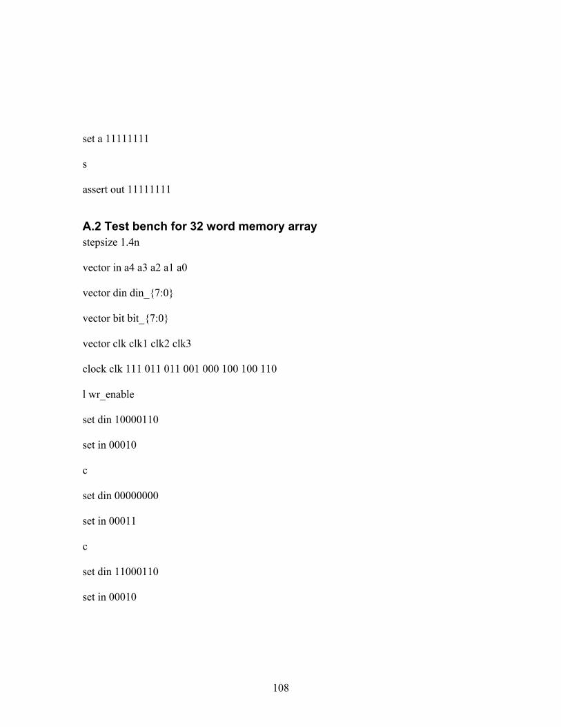
108
set a 11111111
s
assert out 11111111
A.2 Test bench for 32 word memory array stepsize 1.4n
vector in a4 a3 a2 a1 a0
vector din din_{7:0}
vector bit bit_{7:0}
vector clk clk1 clk2 clk3
clock clk 111 011 011 001 000 100 100 110
l wr_enable
set din 10000110
set in 00010
c
set din 00000000
set in 00011
c
set din 11000110
set in 00010

109
c
clear
ana in din bit word3 word2
VITA
KALYAN PARAJULI
Candidate for the Degree of
Master of Science
Thesis: Custom Mask Layout of a 8 bit RISC Microcontroller Major Field: Electrical Engineering Biographical: Personal Data: Born in Kathmandu,Nepal. Son of Baikuntha Prasad Parajuli and Kalpana Parajuli. Education: Graduated from Vivekananda Junior College, Tenali, Andra Pradesh,
India in 1996; received a Bachelor’s Degree of Electrical and Electronics Engineering from Kathmandu University, Dhulikhel, Nepal in September 2000. Completed Requirements for Masters of Science degree with a major in Electrical Engineering at Oklahoma State University in May 2005 .
Experience: Graduate Teaching Assistant, Department of Physics, Oklahoma State
University, 2002-2004