a defect-tolerant accelerator for emerging high...
TRANSCRIPT

A Defect-Tolerant Accelerator for Emerging High-Performance Applications
Olivier Temam
INRIA Saclay, [email protected]
Abstract
Due to the evolution of technology constraints, especiallyenergy constraints which may lead to heterogeneous multi-cores, and the increasing number of defects, the designof defect-tolerant accelerators for heterogeneous multi-coresmay become a major micro-architecture research issue.
Most custom circuits are highly defect sensitive, a singletransistor can wreck such circuits. On the contrary, artificialneural networks (ANNs) are inherently error tolerant algo-rithms. And the emergence of high-performance applicationsimplementing recognition and mining tasks, for which com-petitive ANN-based algorithms exist, drastically expands thepotential application scope of a hardware ANN accelerator.
However, while the error tolerance of ANN algorithms iswell documented, there are few in-depth attempts at demon-strating that an actual hardware ANN would be tolerant tofaulty transistors. Most fault models are abstract and cannotdemonstrate that the error tolerance of ANN algorithms canbe translated into the defect tolerance of hardware ANNaccelerators.
In this article, we introduce a hardware ANN gearedtowards defect tolerance and energy efficiency, by spatiallyexpanding the ANN. In order to precisely assess the defecttolerance capability of this hardware ANN, we introducedefects at the level of transistors, and then assess the impactof such defects on the hardware ANN functional behavior. Weempirically show that the conceptual error tolerance of neuralnetworks does translate into the defect tolerance of hardwareneural networks, paving the way for their introduction inheterogeneous multi-cores as intrinsically defect-tolerant andenergy-efficient accelerators.
I. IntroductionEven though transistor count keeps increasing, in the past
few years, ever more stringent technology constraints areforcing to deeply revisit micro-architectures. After energyconstraints motivated a shift from high clock frequencyprocessors to homogeneous multi-cores, the lack of voltagescaling is breeding the so-called “Dark Silicon” [43], [18]
constraint where only a fraction of transistors can be usedsimultaneously due to the limited on-chip power budget.That constraint, in turn, is likely to induce a novel shifttowards heterogeneous multi-cores, composed of a mix ofcores and accelerators, where only a few accelerators areused at any given time. As a result, increasing attentionshould be devoted to the design of accelerators. However,beyond energy, the growing number of defects is becominganother major constraint that will just as severely affect thedesign of micro-architectures [6], [1]. Within the context ofheterogeneous multi-cores, the challenge is then to find notonly energy-efficient, but also defect-tolerant accelerators.
One of the key challenges of the design of acceleratorsis to find the right balance between application scope andefficiency: entirely reconfigurable circuits are known to lackenergy efficiency [31], while the scope of ASICs is naturallytoo limited. We need to design accelerators which can cover areasonable share, though not all, of the application spectrum;the combination of several such accelerators, rather than asingle accelerator, shall bring sufficient application coverage.The GreenDroid project [49], for instance, argues for theintroduction of a large number of custom circuits in orderto tackle a broad range of tasks at a fraction of the energybudget of a core. Another approach is to consider a multi-purpose accelerator, capable of accelerating the key routinesof many applications, such as the loop accelerator of Clark etal. [13]. While highly energy efficient, not only these designsare not meant to be defect tolerant, but they are even moresusceptible to defects than homogeneous multi-cores, wherecore redundancy at least provides a form of defect tolerance.In this article, we introduce and synthesize a multi-purposeaccelerator which can tolerate multiple defects, which canpotentially implement the computational kernels of some ofthe emerging high-performance tasks using alternative ANN-based algorithms, and, like custom circuits, which can achievemore than two orders of magnitude better energy efficiencythan general-purpose cores.
What are the emerging high-performance applications ?Recently, Intel [17] has attracted the attention of the com-munity to RMS (Recognition, Mining and Synthesis) ap-plications, as some of the most important emerging high-performance applications. That effort partly motivated the

development of the PARSEC benchmark suite [5] by Prince-ton University. Many of the PARSEC benchmarks rely onfour categories of algorithms: classification, clustering, sta-tistical optimization and approximation. While the PARSECbenchmarks rely on a varied set of techniques, for each ofthese four kinds of algorithms, ANNs have been shown toprovide a competitive alternative [23]. For at least half ofthe tasks implemented in PARSEC benchmarks (especiallyRecognition and Mining tasks), we can envision replacingthe core computational task with an alternative ANN-basedalgorithm, so that the application scope of an ANN acceler-ator is potentially broad.
Why focusing on Artificial Neural Networks ? The keybenefit of ANNs is that they are intrinsically tolerant totransient or permanent errors. If this property can be trans-lated into the hardware design itself, then a hardware ANNcan become a defect tolerant accelerator. While the potentialdefect tolerance of ANNs is certainly not a new notion, thereare few in-depth attempts at evaluating the defect tolerancecapability of ANNs down to the transistor level. Some ofthe most recent attempts at evaluating the defect tolerancecapability of hardware ANNs [20] still rely on abstractmodels, e.g., stuck-at synapses. In this article, we assessthe impact of transistor-level defects on the functionalityof ANNs. We show that the impact of such defects canbe significantly different from stuck-at synapses. We thenpropose a novel hardware ANN design, which is inherentlydefect tolerant because it does not spatially fold synapses intoan SRAM bank, and neurons into a few hardware operators,as was commonplace in past [25] or recent [33] designs.On the contrary, we show that spatially expanded designsbring significant defect tolerance benefits; they also improveenergy efficiency by bringing storage (synapses) closer tocomputational operators (neurons). We then precisely assessthe defect tolerance capability of our hardware ANN design,i.e., the impact of defects on the accelerator accuracy. Weevaluate the accuracy using a set of classification tasks fromthe UCI machine-learning repository [3], but the ANN designwould be the same for approximation, or clustering tasks;some modifications might be necessary for optimization tasks(because they might rely on the Hodgkin-Huxley neuronmodel [23]), but we leave such extensions for future work.
While hardware ANNs are an old concept [25], [40], theyfell out of favor in the 1990s for three main reasons: (1)from a mathematical standpoint, ANNs were outperformed byother algorithms such as Support Vector Machines (SVMs),(2) at a time when scientific computing formed the bulkof high-performance applications, the application scope ofANNs was restricted, (3) hardware ANNs could not keep pacewith the the speed of software versions run on processors withrapidly progressing clock frequency, exactly like many ofthe parallel architectures with custom processors at the sameperiod. However, all three situations have drastically changed:(1) Deep Networks [34], i.e., ANNs made of a large numberof wide layers, have recently been shown to outperformSVMs [34], (2) a significant fraction of the recognition and
mining tasks can potentially be implemented using ANNs astheir core algorithms, so an ANN-based accelerator might beable to tackle a large share of emerging high-performanceworkloads, (3) the processor clock frequency has mostlystalled, so that a hardware accelerator will now retain anadvantage of about two orders of magnitude in energy andperformance over a software model run on a processor.
As a testimony to the growing adequation between neuralnetwork-based accelerators and important high-performanceapplications, several industrial hardware neural network de-signs have recently appeared. For instance Chakradhar etal. from NEC [10] propose to implement a convolutionalhardware neural network using a modified FPGA, which is afast, albeit moderately energy efficient, design for tackling abroad range of recognition tasks. IBM has even more recentlyintroduced the Cognitive Chip [47], which is meant to be anenergy efficient design, but it is apparently not geared towardsdefect tolerance.
II. A Spatially Expanded Hardware ANN Acceler-ator
We
igh
ts
Ou
tpu
tshid
de
nne
uro
ns
Local memory
Time-Multiplexed
Inputs
w w w w w w
w w w w
Spatially Expanded
Faulty neuron
Inputs
w Weight storage Multiplexed together
Fig. 1: Time-Multiplexed vs. spatially expanded network.
Artificial Neural Networks. We first briefly recall themain principles of ANNs. The most traditional form ofANNs are Multi-Layer Perceptrons (MLPs); we consider a2-layer MLP with one hidden layer, plus the input layer(it contains no neuron). MLPs are feed-forward networks,where information flows from the input layer (l = 0) to theoutput layer (l = 2). Each neuron performs the followingcomputations. Let y
l
j
the output of neuron j at layer l,y
l
j
= f
�o
l
j
�where ol
j
=P
N
l�1i=0
w
l
ji
y
l�1i
, wji
is the synapticweight between neuron i in layer l�1 and neuron j in layer l,N
l
is the number of neurons in layer l, and f is the activationfunction, often the sigmoid f(x) = 1
1+exp
�x
.We use back-propagation [23], the most popular training
algorithm. Formally, the weights are updated as follows:w
l
ji
(t+1) = w
l
ji
(t)+ ⌘�
l
j
(t)yl�1i
(t), where t is the trainingiteration, ⌘ is the learning rate, and �
l
j
is the error gradient,i.e., the direction of the error. At the output layer, the gradient

expression is �lj
(t) = f
0(olj
(t))⇥e
l
j
(t), where e
l
j
is the error(the difference between the network output and the expectedoutput), and in the hidden layer, the gradient expression is�
l
j
(t) = f
0(olj
(t)) ⇥P
N
l+1k=0
�
l+1k
(t)wkj
(t), where f
0 is thederivative of f .
Spatial expansion vs. time-multiplexing. Many previousand recent ANN designs for high-performance are time-multiplexed [25], [33]: only a few hardware neurons areimplemented, and synapses are stored in a separate memorybank, see Figure 1. At each time step, a few neurons ofa layer are temporarily mapped to the network by fetchingthe corresponding synapses; the intermediate output is storedto serve as input for next layer neurons; executing a wholeneural network requires several time steps.
In a spatially expanded feed-forward ANN, the ANNstructure and operation are similar to that of a conceptualANN: the synapses are stored in individual distributed storagelocations at the level of each neuron, and all neurons aremapped into hardware; the data flows combinationally fromthe input layer to the output layer, see Figure 1. Besides theresulting short synaptic weights access latency, the internalsynaptic weights bandwidth is high, not constrained by a sin-gle synaptic storage structure. Finally, decentralized synapticstorage means the synapses (data) are located close to theneurons (operators), resulting in significant energy benefits[21].
0.3
0.4
0.5
0.6
0.7
0.8
0.9
1
10 20 30 40 50 60 70 80 90 100100010000
>10000
Cumulated fraction of all data sets
# Attributes
Fig. 2: Distribution of UCI data sets as a function of the numberof attributes.
Is it possible to spatially expand ANNs for useful tasks? A key parameter that will influence the network size isthe number of attributes of the network, i.e., the numberof inputs. We have collected the number of attributes of all135 applications of the UCI machine-learning repository [3].The example cases in that repository are contributed byresearchers and engineers from various domains in order tostimulate machine-learning research on their applications.
The distribution of the number of inputs for all 135 UCIapplications in Figure 2 shows that more than 92% of UCIdata have less than 100 attributes. A neural network with 90inputs can capture most of these cases (our design choice).
A few applications in the UCI repository have muchmore attributes, e.g., more than 10000, and machine-learningresearchers are often using input sets with a large numberof attributes, such as the MNIST [35] database (handwrittendigits recognition, 784 attributes) in order to exercise theirmachine-learning algorithms. However, our goal is not toexercise machine-learning techniques but to use data corre-sponding to actual problems, from a broad variety of domainsto which machine-learning techniques are applied, hence thechoice of UCI.
Still, the proposed spatially expanded ANN acceleratorcan cope with a larger number of attributes. In that case, wesimply consider our network as a sub-network and partiallytime-multiplex the larger network over it; however, the sizeof our (sub-)network is such that time-multiplexing is con-siderably reduced compared to moderately expanded designs.
Defect tolerance and scalability. In a fully time-multiplexed network with an SRAM bank for storingsynapses, a significant share of the logic is dedicated tothe time-multiplexing process itself: address decoder, routingsynapses to operators, results back to storage, etc. A faultytransistor within this control logic would wreck the acceler-ator.
A spatially expanded neural network has no control logicexcept at the input/output. Because the synaptic weightsstorage is distributed at the level of each neuron, there isno central storage, and no decoding logic for read operations(we still require write decoding logic in our implementation).As a result, one or several faulty neurons or synapses usuallyhave no noticeable effect after re-training.
This defect-tolerance property also improves scalability.Because control logic is vulnerable, it should be implementedwith larger transistors as the technology node scales down; ina spatially expanded network, the smaller fraction of controllogic has a lesser impact on scalability.
If the spatially expanded network is used in a partiallytime-multiplexed mode, it remains tolerant to defects. How-ever, a defect at a given hardware neuron would affectall the neurons of the application network mapped to it,effectively multiplying the number of defects by as much asthe multiplexing factor.
III. Injecting Transistor-Level DefectsA. Hardware Faults
The classic hardware fault model is the stuck-at model[32], where an input gate signal is considered stuck at 0 or 1.This fault model is appropriate for test purposes because thegoal is to find faults, and then to suppress them. So the goalis not so much to accurately capture the gate behavior for anyinput, but to do so with enough inputs that the fault can bedetected. Even though we leverage test techniques, our goalis different: we will not suppress the faults, we will use thecircuit with the faults. However the actual behavior of a faultyANN circuit can potentially influence the ability of the ANNto cope with faults, and the ability of the training algorithm

DMACtrl
w
x
w
x... ...........................
w
x
w
x...
Acce
lera
tor
Mem
ory
inte
rface
Time-Multiplexing add-ons128 Network
16
+ +
Fig. 3: Accelerator implementation (memory interface & hiddenlayer).
ax+b
x
LUT
x (input)
*+a
bf(x)
Index
Fig. 4: Sigmoid: piecewise approximation and hardware imple-mentation.
to silence out faulty parts. Therefore, unlike for test purposes,we need to model as accurately as possible the behavior of thefaulty circuit, not just determine that it is faulty; and we willhighlight that logic gate-level hardware faults can exhibit asignificantly different behavior than transistor-level hardwarefaults. Failing to accurately account for the behavior of faultyhardware ANNs means that claims of their defect tolerancewould remain fairly baseless, or at least unproven.
Traditionally used in circuit-level testing, the stuck-at gatemodel has been adopted by the micro-architecture communityin the form of latch bits stuck at 0 or 1 [41], [37]. Such amodel accurately describes faults occurring at state elements(latches, registers, SRAM), but it inaccurately describes faultsoccurring within logic elements (control and logic operatorsin processors or ASICs). However, in a spatially expandedneural network, logic operators account for a large share ofthe accelerator footprint. Recently, a more accurate gate-levelmodel has been proposed by Li et al. [36], where hardwarefaults are modeled as stuck (or delayed) inputs of logic gates.While this model is a significant progress over latch-levelbit flips, the actual behavior of logic blocks resulting fromtransistor-level defects can often be more complex than stuck-at and delayed inputs of logic gates, in part because they occurwithin the complex gates often used in modern CMOS design[42].
The two main types of transistor-level defects are shortsand opens (either full or partial ones, between the source and
the drain, or between the gate and the drain/source) [32], [4].For instance, shorts can correspond to insufficient metal beingremoved during photolithography, and opens to an excess ofmetal being removed (or an excess of insulating material).Shorts and opens can force transistor paths to be (or appear)stuck open or closed, or create bridges between transistors, orinduce delays. In many cases, the impact of these hardwarefaults on the logic gate function cannot be modeled usinga stuck logic gate input: for instance, the logic gate functionwill be changed, or it will be transformed into a state element,or it can depend on free floating devices, etc.
As a result, we factor in the impact of transistor-leveldefects at the level of logic gates. Starting from an RTLgate-level logic function, we transform it into a transistorschematic, inject any number of transistor-level shorts oropens, and reconstruct the new transformed logic function(or state element) corresponding to the altered schematic.
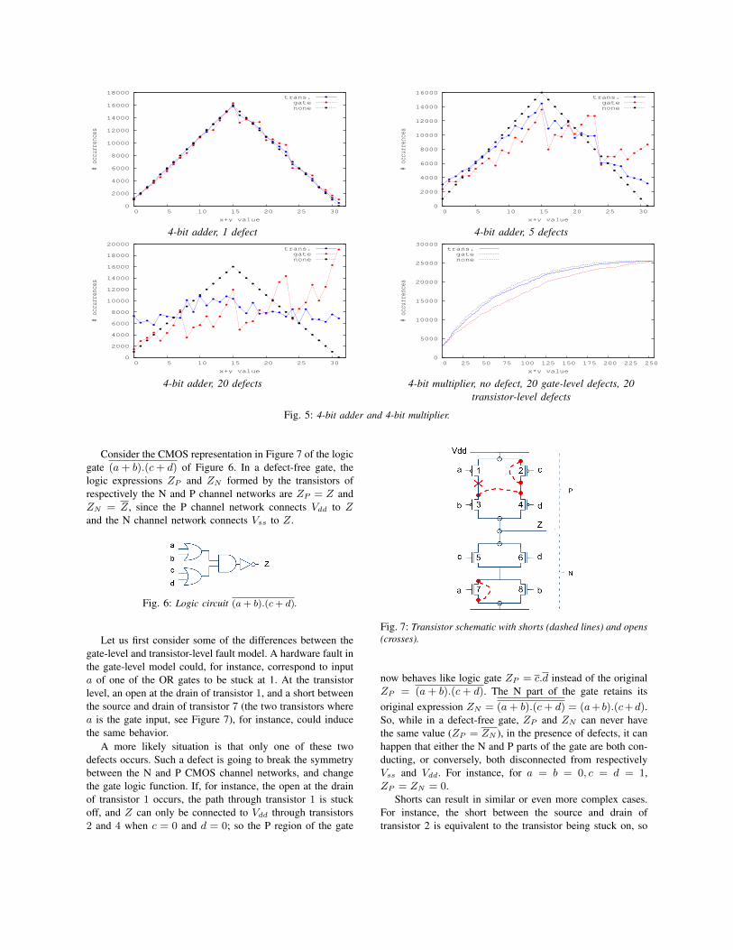
In order to illustrate the behavior discrepancy betweengate-level defect injection and transistor-level defect injection,we inject a random number of defects in adders and multipli-ers (the key logic operators of the neural network); we use 4-bit adders and multipliers in this example, while the networkuses 16-bit operators. The defects are randomly spread overthe operator bits, and within each 1-bit operation, over alltransistors. Then we consider all possible combinations ofthe two 4-bit inputs, and collect the distribution of the valuesof the output. We present the 4-bit input pairs in randomorder in order to avoid any special behavior related to thememory property induced by some faults. The results areshown in Figure 5 for 1, 5 and 20 defects injected in the 4-bit adder, and 20 defects injected in the 4-bit multiplier. Thedotted (black) line corresponds to the distribution of valuesof the error-free sum (see none), the dashed (red) line tothe defects injected at the gate level, and the solid (blue) lineto the defects injected at the transistor level. We repeat thisexperiment 1000 times (injecting different defects each time),and collect the total distribution over these 1000 iterations.
For 1 defect, the behavior of the 4-bit adder is barelyaffected. As the number of defects increases from 5 to 20,the distribution of values becomes increasingly different fromthe actual sum distribution. However, the profile for transistor-level defects remains closer to the error-free profile than thegate-level defects profile. At 20 defects, the gate-level profileis barely related to the error-free profile. A similar behaviorcan be observed for the multiplier. In other words, for suchfundamental operators as the adder and the multiplier, it canbe observed that transistor-level and gate-level defects inducesignificantly different behavior.
B. From Transistor Defects to Logic ExpressionThe goal of this section is twofold: to illustrate why
transistor-level and intra-gate defects can induce significantlydifferent gate-level behavior than stuck-at gate input defects,and to explain how a logic function (or state element) can bereconstructed after transistor-level defect injection, in orderto emulate the behavior of a faulty circuit.
0
2000
4000
6000
8000
10000
12000
14000
16000
18000
0 5 10 15 20 25 30
# oc
curr
ence
s
x+y value
trans.gatenone
4-bit adder, 1 defect
0
2000
4000
6000
8000
10000
12000
14000
16000
0 5 10 15 20 25 30
# oc
curr
ence
s
x+y value
trans.gatenone
4-bit adder, 5 defects
0
2000
4000
6000
8000
10000
12000
14000
16000
18000
20000
0 5 10 15 20 25 30
# oc
curr
ence
s
x+y value
trans.gatenone
4-bit adder, 20 defects
0
5000
10000
15000
20000
25000
30000
0 25 50 75 100 125 150 175 200 225 250
# oc
curr
ence
s
x*y value
trans.gatenone
4-bit multiplier, no defect, 20 gate-level defects, 20transistor-level defects
Fig. 5: 4-bit adder and 4-bit multiplier.
Consider the CMOS representation in Figure 7 of the logicgate (a+ b).(c+ d) of Figure 6. In a defect-free gate, thelogic expressions Z
P
and Z
N
formed by the transistors ofrespectively the N and P channel networks are Z
P
= Z andZ
N
= Z, since the P channel network connects V
dd
to Z
and the N channel network connects V
ss
to Z.
Fig. 6: Logic circuit (a+ b).(c+ d).
Let us first consider some of the differences between thegate-level and transistor-level fault model. A hardware fault inthe gate-level model could, for instance, correspond to inputa of one of the OR gates to be stuck at 1. At the transistorlevel, an open at the drain of transistor 1, and a short betweenthe source and drain of transistor 7 (the two transistors wherea is the gate input, see Figure 7), for instance, could inducethe same behavior.
A more likely situation is that only one of these twodefects occurs. Such a defect is going to break the symmetrybetween the N and P CMOS channel networks, and changethe gate logic function. If, for instance, the open at the drainof transistor 1 occurs, the path through transistor 1 is stuckoff, and Z can only be connected to V
dd
through transistors2 and 4 when c = 0 and d = 0; so the P region of the gate
Fig. 7: Transistor schematic with shorts (dashed lines) and opens(crosses).
now behaves like logic gate Z
P
= c.d instead of the originalZ
P
= (a+ b).(c+ d). The N part of the gate retains itsoriginal expression Z
N
= (a+ b).(c+ d) = (a+ b).(c+d).So, while in a defect-free gate, Z
P
and Z
N
can never havethe same value (Z
P
= Z
N
), in the presence of defects, it canhappen that either the N and P parts of the gate are both con-ducting, or conversely, both disconnected from respectivelyV
ss
and V
dd
. For instance, for a = b = 0, c = d = 1,Z
P
= Z
N
= 0.Shorts can result in similar or even more complex cases.
For instance, the short between the source and drain oftransistor 2 is equivalent to the transistor being stuck on, so

Fig. 8: B-Block and its truth table; logic expression of Z using aB-Block for the example of Figures 6,7 with short between sourceand drain of transistor 2.
Z can be connected either when a = b = 0 or when d = 0,so Z
P
= a.b + d = (a+ b).d. The short connecting thedrain of transistor 1 and the drain of transistor 2 would affectthe logic expression of Z
P
in a more subtle way. Transistors1 and 2 are now in parallel, as well as transistors 3 and 4,so Z is connected to V
dd
if a = c = 0 or a = b = 0 orc = b = 0 or c = d = 0, so the expression of Z
P
is changedto Z
P
= a.d+ a.b+ c.b+ c.d = (a.c) + (b.d). Again, thereare cases where Z
N
= Z
P
.What happens when Z
N
= Z
P
and how to reconstruct alogic function expression with asymmetric N and P channelnetworks ? When Z
P
= 1 and Z
N
= 1 simultaneously, bothV
ss
and V
dd
are connected to Z but the path from ground(Z
N
) dominates and the output is pulled to the logic value 0[27].
When Z
P
= 0 and Z
N
= 0 simultaneously, there is nopath from either V
ss
or V
dd
to Z, so the output retains itsprevious value, there is a memory effect [32].
As a result, with asymmetric N and P channel networks,not only the logic expression of Z has changed (becauseof case Z
N
= Z
P
= 1) but it has also become a stateelement (because of case Z
N
= Z
P
= 0). This state elementcan be modeled with a B-block gate [27] and its truth tableis shown in Figure 8. Using this B-block, it is possibleto give a logic representation of the asymmetric transistorschematic resulting from opens and shorts, as shown in Figure8. The main feature is that the B-block allows to separatelyreconstruct the N and P-channel network logic functions, andto later combine them so as to obtain the gate logic value.
A delay due to partial shorts and opens, or gate todrain/source shorts, etc, can also be inserted anywhere in theN or P channel networks, breaking up the corresponding logicfunction into two sub-functions. It takes the form of a stateelement that stores the line value and propagates it at the next
transition(s).The process for injecting transistor-level defects and ob-
taining an altered logic expression can be summarized asfollows:
1) Logic to schematic. The first step is to convert thelogic function into a CMOS transistor schematic, andto inject defects, see Figure 9(a).
2) TLogic nodes. During the reconstruction process, fromthe transistor schematic to the logic function, the no-tion of TLogic (Transistor-Logic) nodes is introducedin order to represent gates with a source and drain,i.e., partially converted transistors; these hybrid gatescorrespond to transistor bundles, on which transistor-to-logic conversion rules can still be applied as if theywere transistors. See a TAND in Figure 9(c).
3) Splitting connections. Hardware defects introduceasymmetries in the schematic that can prevent the re-construction into a logic function. In order to overcomethe asymmetry, some connections need to be split,sometimes at the cost of virtually replicating transistors.See connection j2 split into j2, j
02 in Figure 9(d).
4) Bypasses. Some hardware defects, such as bridges, canresult in bypasses which void the functional role ofsome transistors. As a result, these transistors can beeliminated when reconstructing the transistor schematicinto a logic function. See bypass j1 ! j4 resulting inthe elimination of serial transistors e and b, in Figure9(e).
5) TLogic to Logic. The final step consists in convertingremaining TLogic gates into normal logic gates, essen-tially removing the source and drain connections. SeeFigure 9(f,g).
We have implemented these different steps as one auto-mated process in order to assess different neural networksorganizations and operators (e.g., different sigmoid functions,different implementations of arithmetic operators, etc).
Currently, one of the main limitations of the approachis that transistor layout is not factored in. In the future, weplan to introduce a simplified form of layout in order toknow which transistors are physically close, and thus mostsusceptible to endure bridging effects, for instance.
IV. Hardware ANN Implementation
In this section, we briefly introduce the hardware neuralnetwork in which we will be injecting defects.
Overview. A scaled down version of the spatially ex-panded hardware neural network accelerator is shown inFigure 3; the actual network contains 90 inputs, 10 hiddenneurons and 10 outputs. The number of inputs and outputsare selected based on the typical number of attributes andclasses in the examples of the UCI repository, as explainedin Section II. The number of hidden neurons (10) is the besttrade-off between accuracy and cost for the example caseswe consider, see Section V. The network is fully connected.

Fig. 9: (a) Bridge defect between connections j1 and j4; (b) resulting transistor schematic; (c) first replacement of transistors c andd with TAND(c,d); (d) splitting connection j2; (e) bypass j1 ! j4 voids transistors b (between j7 and j2) and e (between j2 and j4),and transistor b is serially connected with TAND(c,d); (f) transforming Tlogic into plain logic; (g) reconstructed logic function.
There are two main types of application scenarios forclassifiers: off-line training where the classifier is trained thendelivered (and periodically retrained when necessary), andon-line training where the classifier is continuously trained.The latter scenario usually corresponds to smart sensors andindustrial control, while the former scenario corresponds tothe high-performance processing of large volumes of dataand is the most typical scenario. We focus our acceleratordesign on that scenario, and perform the ANN training in acompanion core, though using the forward hardware logic.Therefore, if a defect occurs within the hardware ANN, theretraining will factor in the faulty elements. The acceleratorcan also be extended to include training hardware for tacklingboth the on-line and off-line scenarios.
Input/Output.Fetching input rows. We use a DMA for efficiently
fetching the input rows. The DMA uses a 2-latch bufferfor each input in order to let the accelerator use one rowwhile it fetches the next. Similarly, the DMA uses a 2-latchoutput buffer for each output. The accelerator and the DMAcommunicate through a simple 2-signal handshaking protocol(ready/accept).
Writing synaptic weights during training. We use the sameinterface for fetching input rows, and for writing synapticweights (during training). For that purpose, each internal wireis connected to both the input of multipliers and the synapticweights input latches, see Figure 3. Each neuron of layer l
is reloaded one by one: all its N
l�1 synaptic weights areloaded, then stored. A write signal wl
j
, for neuron j at layer
l, is activated by the DMA. Then the synaptic weights of thenext neuron are loaded, etc.
Fixed-Point computations. Even though many softwareimplementations of ANNs rely on floating-point computa-tions, this is usually overkill [16]. Fixed-Point computationswith as little as 8 bits have been shown to achieve similaraccuracy for a broad range of problems [24], and as a result,many past hardware implementations have relied on fixed-point arithmetic with a limited number of bits. In order toconsider a sufficiently broad set of problems, we opt for a16-bit design, with a 6-bit integral part, 10-bit decimal part.We empirically checked that, for all the problems we considerin this article, this 16-bit design allows to achieve the sameaccuracy as a floating-point design.
Activation function. The sigmoid function implementsthe non-linear behavior of artificial neurons. We implementthis function using a piecewise linear approximation usinga small look-up table (x ! f(x) = a
i
⇥ x + b
i
), whereeach table entry contains the pair of coefficients (a
i
, b
i
), seeFigure 4. Each segment i applies to a limited range of theinput value x. We empirically observed that approximatingthe function with 16 segments has no noticeable impact onthe network accuracy compared to the original sigmoid. Theactivation function characteristics are reported in Table IIIusing the Synopsys Design Compiler at 90nm; the latencycorresponds to the computation of f(x) (read access to theLU, multiplication then addition).
Partial time-multiplexing. For the problems which donot fit in the spatially expanded network, we can still resort

to time-multiplexing. All neurons of the network are thenconsidered to belong to one large layer. As a result, we mustnow be able to directly feed inputs to neurons in the outputlayer, or collect the output of neurons in the hidden layer.For that purpose, we alter the design in several ways, seeadd-ons in grey in Figure 3. We add as many input latchesas the number of hidden neurons, and connect these inputlatches to the internal buses between the hidden and outputlayers. These input latches can feed input values directly tothe neurons of the output layer. And the output of the hiddenneurons is connected to the additional output latches. As aresult, all neurons can now be used as if they were part of asingle layer.
Processing one input row of a neural network whichcontains N times the number of neurons of the hardwareneural network requires at least N times the delay necessaryto process one input row in the hardware neural network.
V. Experimental FrameworkWe implement the accelerator and the memory interface
in Verilog and synthesize them with the Synopsys DesignCompiler, using the TSMC 90nm library.
We have developed two other software models of the artifi-cial neural network. One model is meant for network trainingand testing, training is performed using back-propagation;this model has been validated against the FANN library [44].The model is also used to inject hardware defects as laterexplained in Section VI-C. The second model is just meantfor feed-forward testing within the processor simulator. It isoriented towards very fast execution, and it is a trimmed downversion of a neural network which performs only the sameoperations as the hardware version, albeit in C.
For the superscalar processor, we use Wattch/SimpleScalarand configured the processor so that it roughly emulates anIntel Stealey (A110) core [14]. Our goal is to compare theaccelerator against a low-power high-performance core, suchas the Intel Atom, using the same 90nm technology node.While the Atom was first implemented in the 45nm process,the Stealey (A100 and A110), derived from the Pentium Mand implemented at 90nm, is considered a predecessor of theAtom. The Stealey is a 800MHz, 3W processor.
While the initial version of Wattch was designed fora 350nm technology [8], the 100nm technology has beenadded to version 1.02. We use the fudge factor to furtherslightly scale down the technology to 90nm. Wattch has anapproximate evaluation of leakage power, however at 90nm,leakage power is still roughly less than 30% of total power[38]; moreover, we will see later on that the energy differencebetween the processor and the accelerator is such that thislack of precision on leakage power is tolerable. It could bemore significant with much smaller technology nodes.
The trimmed down software model is compiled into Alphabinary using the crosstools [28], and the -O optimizationlevel. The overhead of the initialization and readout steps arerendered negligible by executing the ANN computations for1000 input rows.
Hyper Parameter From To Step# Hidden neurons 2 16 +2# Epochs 100 3200 *2Learning rate 0.1 0.9 +0.1Momentum 0.1 0.9 +0.1
TABLE I: Hyper-Parameter space.
Problem Description # In, ⌘,# Out # Epochs,
# Hiddenbreast Breast cancer 30, 2 0.1,
diagnostic 200, 14glass Glass oxides 9, 6 0.1,
identification 800, 10(forensic)
ionosphere Radar returns from 34, 2 0.3,ionosphere 100, 6
iris Plants 4, 3 0.2,classification 100, 8
optdigits Handwritten digits 64, 10 0.1,recognition 200, 14
robot Failure 90, 5 0.2,detection 1600, 6
sonar Metal vs. Rock 60, 2 0.1,sonar returns 100, 10
spam Email spam 57, 2 0.1,identification 800, 6
vehicle Vehicle silhouettes 18, 4 0.1,recognition 400, 6
wine Wine origin based 13, 3 0.2,on chemicals 1600, 4
TABLE II: # Inputs (attributes) and outputs (classes), and besthyper-parameters (⌘ = learning rate, hidden = optimal # ofhidden neurons).
We have selected 10 applications from the UCI Machine-Learning repository to serve as a “benchmark” suite [3]. Thetwo selection criteria were application diversity and havingless than 100 attributes. The data characteristics are summa-rized in Table II. For each application, we have searched theoptimal accuracy within a hyper-parameter space indicatedin Table I. We report the main optimum training hyper-parameters (epoch, learning rate) in Table II. All accuracymeasurements provided in the remainder of the article uses10-fold cross validation. The network is trained using MSE(Mean Squared Error) though we report accuracy measure-ments.
VI. Evaluation
A. Accelerator area, energy, latency and accuracy char-acteristics
We evaluate the area cost, latency and energy of thenetwork using the Synopsys Design Compiler. The energyincludes both the dynamic and leakage power. The neuralnetwork accelerator characteristics are provided in Table III.At 90nm, the accelerator footprint is 9.02mm2, the totaldissipated power is 4.70W, the time to process one input rowis 14.92ns, and the total energy spent per input row is 70.16nJper row.

Characteristic Accelerator Activation InterfaceTime (in ns) 14.92 ns 2.84 nsFreq. (in Mhz) 800Area (in mm2) 9.02 0.017 0.047Power (in W) 4.70 0.0019 0.0054Energy per input row 70.16 0.0053 0.0021(in nJ)
TABLE III: Accelerator, memory interface and activation func-tion characteristics.
Characteristic ValueClock frequency 800MHz# cycles per row 19680Avg. power per cycle 2.78(in W)Energy per row (in nJ) 68388
TABLE IV: Processor execution characteristics.
Memory interface and key logic. We have separatelyevaluated the characteristics of the memory interface becauseit is part of the key logic, i.e., logic that cannot be scaleddown like the ANN logic because it must be defect-free.The memory interface includes the DMA controller, whilethe write signals for synaptic weights latches, the controlsignals for connecting the output of the hidden neurons, andthe additional input latches (for partial time-multiplexing) tothe internal wires are included in the key logic.
The target network configuration has 90 attributes, so90⇥16 = 1440 bits must be loaded to feed one input row tothe neural network. To maximize the accelerator throughput,1440 bits must be fetched every 14.92 nanoseconds, i.e.,11.23GB/s; these numbers are in line with the bandwidth ofthe recent Intel Quick Path Interconnect [39], for instance(12.8GB/s in one direction). We assume two links capable ofbringing 64 bits each every cycle, and must clock the interfaceat 754MHz, or higher, for achieving the maximal processingbandwidth of the accelerator (11.23GB/s); we use 800MHz.The memory interface characteristics are reported in TableIII.
At 90nm, the interface and key logic area accounts for anegligible amount of the overall accelerator area. Assuminga factor of area size reduction of 2 across technology nodes,with the interface and key logic area remaining constant,it would only account for less than 10% of the overallaccelerator area after 4 technology generations (22nm), and25% at the 6th generation (11nm). Moreover, the numberof neurons in the accelerator can also be scaled up acrossgenerations, further reducing the relative overhead.
B. Accelerator vs. processor
Characteristics of processor execution. As mentioned inSection V, we simulate a trimmed down software model sothat it performs almost the same operations as the hardwareaccelerator.
Since we assume an identical underlying memory system,and since we do not aim at comparing DMA vs. memoryhierarchy and hardware prefetching, we restrict the compari-son to the accelerator and the processor. For that reason, weassume a perfect 1-cycle L1 cache, and subtract the powerand energy used by the L1 and L2 caches. The 1-cycle perfectcache aims at bringing the processor-to-memory latency at thelevel of a DMA, and to avoid biasing the comparison towardsthe neural network with a more efficient memory subsystem.
We clock the processor at 800MHz, the maximal fre-quency of the Intel Stealey, and the same as for the DMA.
The performance characteristics of the processor run areshown in Table IV for a 90-10-10 software ANN. The numberof cycles and energy are provided per input row, i.e., for eachset of 90 inputs. The measured accelerator power (4.70W)is actually higher than the processor power (2.78W) due tothe large number of computing elements in the accelerator.But the energy consumed by the accelerator (70.16 nJ perrow) is drastically lower than that of the processor (68388nJ per row) because processing one input row requires only14.92ns in the accelerator, thanks to the massive parallelmultiplications/additions and circuit-level parallelism, whileit requires 19680 cycles in the processor, i.e., 24600ns at800MHz.
While high, this energy ratio is consistent with previousresearch, such as the work by Hameed et al. [21], whichreports a slightly lower energy ratio of 500x for an H264decoder run on a general-purpose core and implemented asa custom circuit; Chung et al. [12] report lower ratios ofabout 100x, but both studies factor in the impact of memoryaccesses, while the numbers reported in Table III are for theaccelerator only, as mentioned above. Other accelerators canalso provide significantly better energy efficiency than cores,especially GPUs and FPGAs. While precise energy ratios canvary wildly across applications, architectures and technology,GPUs and FPGAs can roughly be an order of magnitude moreenergy efficient than CPUs [12], and FPGAs are at least anorder of magnitude less energy efficient than ASICs [12],[31].
C. Defect ToleranceIn order to evaluate the impact of defects, we randomly
pick one of the logic operators or latches within the input andhidden layers, and one 1-bit operator or wire within the targetoperator or latch. The operator is then altered because of thedefect, and replaced by a reconstructed logic gate function,according to the process described in Section III-B. In ourhigh-level ANN software model used for training and testing,it is possible to mark a neuron as having one or severaldefect(s) for a specific operator, in which case a softwarefunction is called to perform that operator in place of thenative operator.
The impact of such defects, as a function of the number ofdefects, is shown in Figure 10. For each number of defects,we report the accuracy obtained after re-training, in orderto demonstrate the network capacity to silence out defects.

0
0.1
0.2
0.3
0.4
0.5
0.6
0.7
0.8
0.9
1
0 3 6 9 12 15 18 21 24 27
Accuracy
# Defects
winebreastglass
ionosphereiris
robotsonar
vehiclespam
optdigits
Fig. 10: Accuracy vs. # of defects in input and hidden layers.
0
0.1
0.2
0.3
0.4
0.5
0.6
0.7
0.8
0.9
1
0.001 0.01 0.1 1 10 100 1000
Accuracy
Error amplitude
winebreastglass
ionosphereiris
robotsonar
vehiclespam
optdigits
Fig. 11: Accuracy vs. # error amplitude in the output layer.
We reproduce the experiment 100 times, each time randomlyvarying the component where the defects occur; howeverthe N defects of a network remain the same while thenetwork is re-trained and tested on all target problems. Forall applications considered, the accelerator can tolerate upto 12 defects, independently of which bit is affected, andmost applications are not significantly affected by up to 20defects. Even if errors occur on bits which significantly swaythe neuron output, the neuron can be silenced by re-training.Afterward, accuracy can degrade sharply as too many neuronsare affected.
In the output layer, a defect occurring at the activationfunction, or the adder just before the activation function,has a strong influence, though the rescaling effect of theactivation function may tame it. In such cases, the networkaccuracy is fairly sensitive to the amplitude of the errorintroduced by the defect, as it directly affects the class value(or prediction). Within a digital neural network, the amplitudeof the error depends on the position of the bit which incurredthe error. We have introduced single defects in either of thetwo most sensitive parts of the output layer (adders, activationfunctions). For each such randomly generated faulty network,we evaluate the network accuracy after re-training; for each
individual input row during the network test phase, we alsomeasure the error amplitude at the adder output of the faultyneuron (the absolute value of the difference between theoutput of that adder with and without the defect). We thenreport the average accuracy as a function of the amplitudein Figure 11. For about half of the applications, such asionosphere, the accuracy remains high as long as the erroramplitude is not such that it can sway the class. However, forsome applications, such as iris and robot, even tiny errorscan sway the class and affect the accuracy.
Consequently, the adders and activation functions of theoutput layer should be considered a defect-sensitive part ofthe accelerator. For our network, these elements account for25.9% of the output layer, and 2.3% of the total area. Thereare two possible ways to improve the defect tolerance ofthese elements of the network layer: consider the adders andactivation functions of the output layer as key logic, or simplyadd spare (redundant) output neurons. The former solution ispreferable as long as the fraction of the overall area coveredby the output adders and activation functions is small; astechnology scales down, the latter method will become morearea efficient.
VII. Related Work
On hardware neural networks, there is a large body ofwork and it would not be possible to cite a representativesubset here. Multiple implementations have been proposed,including commercial ones [15], such as the Intel ETANN[25], or recent ones for high-performance multimedia pro-cessing [33], but most are time-multiplexed. Some hardwarenetworks are meant for industrial control [7], and others forsmart sensor applications; many of the latter designs are low-power analog (or mixed-mode digital/analog) neural networks[48]. Analog logic is attractive because it is dense and lowpower, but the energy reductions and performance improve-ments are limited by their sensitivity to noise (temperature,mismatch,. . . ). Moreover, noise accumulates over long chainsof operators, limiting the number of bits carried per wire [9],or requiring to frequently convert into the digital domain forrestoring the signal. Still, small-scale analog networks havebeen successfully shown to be applicable to high-performancesystems, for instance for efficiently implementing a percep-tron branch predictor [2]. Another popular field of researchfor analog hardware neural networks is biological emulation,with up to 60 million analog neurons implemented on onefull wafer [46], but such implementations are only remotelyrelated to computing applications.
While there is a large body of work on defect tolerancein hardware neural networks as well, there are few workssimultaneously addressing high-performance, low-power anddefect tolerance issues, especially at the transistor level. A notso recent but interesting example is the Philips LNeuro [40]which had to fulfill all these criteria due to a projected appli-cation in a satellite; though the design is time-multiplexed, itis modular for both scalability and reliability purposes. Most

of the research work on defect models for neural networksfocus on the stuck-at-0 or stuck-at-1 defects in synapticweights [20], [45], [22]. Special training algorithms have alsobeen proposed to compensate for such stuck-at defects [26].
Beyond neural networks, there are several successful at-tempts at tackling transient faults or permanent defects withinexisting or modified processor architectures. Kumar et al.[30] show how a combined hardware and software approachcan detect the occurrence of many transient faults. Kruijfet al. [29] introduce the notion that a degree of hardwareinaccuracy can be tolerated provided the impact of errorson applications is controlled with algorithm-specific metrics.Chakrapani et al. [11] have even introduced transistor-leveltradeoffs between energy and algorithm accuracy (PCMOS)and demonstrated applications to low-power ASICs; recently,Esmaeilzadeh et al. [19] have used similar concepts withinprocessors themselves.
The approach used for determining the impact of hardwaredefects on the functional behavior of the neural networkleverages existing test techniques [32], including expressingthe impact of transistor-level defects, such as bridges [42], atthe level of gates. However, unlike test techniques, the goal isnot to find the appropriate test sequences which will allow toidentify errors, but to attempt to reconstruct the output of thefaulty circuit. Banerjee et al. [4] have shown that transistor-level defects cannot be modeled only using stuck-at faults atthe input of logic gates, and can manifest themselves in manyother ways (modification of the logic function, introductionof state, delays, etc). Alam et al. [1] recently outlined currenttrends in VLSI defects.
VIII. Conclusions and Future Work
Due to technology constraints, micro-architecture researchmay progressively shift its focus to accelerators, and espe-cially energy-efficient and defect-tolerant accelerators. Wemake the case for hardware neural networks to be consideredas one of the possible candidate accelerators. While hardwareneural networks have already been considered in the past, weargue that the situation has drastically changed in terms oftechnology constraints, application scope, and even machine-learning algorithms. We outline the differences between past(time-multiplexed) designs and our proposed spatially ex-panded design, and especially that spatial expansion bringsbenefits in energy and defect tolerance. We particularly focuson validating and quantifying the intrinsic defect tolerancecapabilities of hardware neural networks in the presenceof transistor-level faults. The defect tolerance of neuralnetworks proves to be not just a conceptual notion, but anactual property of hardware neural networks, provided theneural network is periodically retrained. As a result, it pavesthe way for hardware accelerators intrinsically capable ofcoping with hardware faults, without having to identify anddisable the faulty parts.
We are currently working on two follow-up research paths.First, we want to illustrate the potentially broad application
scope of a hardware neural network accelerator by demon-strating competitive implementations of multiple emerginghigh-performance tasks using neural network algorithms andrun on a hardware neural network accelerator. Second, wewant to increase the size of the neural networks that canbe mapped without time-multiplexing, in order to efficientlytackle very large networks, such as Deep Networks. Forthat purpose, we are investigating three different approacheswhich could ultimately be combined: analog neurons fordenser and more energy-efficient neurons, 3D stacking forthe dense implementation of multiple network layers, andmemristors for the dense implementation of synapses.
AcknowledgmentsWe would like to thank the anonymous reviewers for theirhelpful comments and advices.
References
[1] M. Alam, K. Roy, and C. Augustine. Reliability- and process-variation aware design of integrated circuits - a broader per-spective. In Reliability Physics Symposium (IRPS), 2011 IEEEInternational, pages 4A.1.1 –4A.1.11, april 2011.
[2] R. S. Amant, D. A. Jimenez, and D. Burger. Low-power, high-performance analog neural branch prediction. In InternationalSymposium on Microarchitecture, pages 447–458, 2008.
[3] A. Asuncion and D. Newman. UCI machine learning repository,2007.
[4] P. Banerjee and J. A. Abraham. Characterization and testing ofphysical failures in mos logic circuits. IEEE Design and Test,pages 76–86, Aug. 1984.
[5] C. Bienia, S. Kumar, J. P. Singh, and K. Li. The parsec bench-mark suite: Characterization and architectural implications. InProceedings of the 17th International Conference on ParallelArchitectures and Compilation Techniques, October 2008.
[6] S. Borkar. Design perspectives on 22nm cmos and be-yond. In Design Automation Conference, 2009. DAC ’09. 46thACM/IEEE, pages 93 –94, july 2009.
[7] B. K. Bose. Neural network applications in power electronicsand motor drives – an introduction and perspective. IndustrialElectronics, IEEE Transactions on, 54(1):14–33, Feb. 2007.
[8] D. Brooks, V. Tiwari, and M. Martonosi. Wattch: a frameworkfor architectural-level power analysis and optimizations. InISCA ’00: Proceedings of the 27th annual international sympo-sium on Computer architecture, pages 83–94, New York, NY,USA, 2000. ACM.
[9] S. Chakrabartty and G. Cauwenberghs. Sub-microwatt analogvlsi support vector machine for pattern classification and se-quence estimation. In Advances in Neural Information Pro-cessing Systems (NIPS), Dec. 2004.
[10] S. Chakradhar, M. Sankaradas, V. Jakkula, and S. Cadambi. Adynamically configurable coprocessor for convolutional neuralnetworks. In International symposium on Computer Architec-ture, page 247, Saint Malo, France, June 2010. ACM Press.
[11] L. N. Chakrapani, P. Korkmaz, B. E. S. Akgul, and K. V. Palem.Probabilistic system-on-a-chip architectures. ACM Transactionson Design Automation of Electronic Systems, 12(3), August2007.
[12] E. S. Chung, P. A. Milder, J. C. Hoe, and K. Mai. Single-chip heterogeneous computing: Does the future include customlogic, fpgas, and gpgpus? In MICRO, pages 225–236. IEEE,2010.

[13] N. Clark, A. Hormati, and S. Mahlke. Veal. In InternationalSymposium on Computer Architecture, pages 389–400, Beijing,June 2008.
[14] I. Corporation. Intel processor a100 and a110 on 90 nm processdatasheet, January 2008.
[15] F. M. Dias, A. Antunes, and A. M. Mota. Artificial neuralnetworks: a review of commercial hardware. EngineeringApplications of Artificial Intelligence, 17(8):945 – 952, 2004.
[16] S. Draghici. On the capabilities of neural networks using limitedprecision weights. Neural Netw., 15(3):395–414, 2002.
[17] P. Dubey. Recognition, mining and synthesis moves computersto the era of tera. TechnologyIntel Magazine, 09, Feb 2005.
[18] H. Esmaeilzadeh, E. Blem, R. S. Amant, K. Sankaralingam, andD. Burger. Dark Silicon and the End of Multicore Scaling. InProceedings of the 38th International Symposium on ComputerArchitecture (ISCA), June 2011.
[19] H. Esmaeilzadeh, A. Sampson, L. Ceze, and D. Burger. Archi-tecture support for disciplined approximate programming. InT. Harris and M. L. Scott, editors, ASPLOS, pages 301–312.ACM, 2012.
[20] J. Fieres, J. Schemmel, and K. Meier. A convolutional neuralnetwork tolerant of synaptic faults for low-power analog hard-ware. Lecture Notes in Artificial Intelligence, 4087:122–132,2006.
[21] R. Hameed, W. Qadeer, M. Wachs, O. Azizi, A. Solomatnikov,B. C. Lee, S. Richardson, C. Kozyrakis, and M. Horowitz.Understanding sources of inefficiency in general-purpose chips.In International Symposium on Computer Architecture, page 37,New York, New York, USA, 2010. ACM Press.
[22] A. Hashmi, H. Berry, O. Temam, and M. H. Lipasti. Automaticabstraction and fault tolerance in cortical microachitectures. InISCA 2011, San Jose, 2011.
[23] S. Haykin. Neural Networks. Prentice Hall Intl, London, UK,2nd edition, 1999.
[24] J. Holi and J.-N. Hwang. Finite precision error analysis ofneural network hardware implementations. IEEE Transactionson Computers, 42(3):281–290, 1993.
[25] M. Holler, S. Tam, H. Castro, and R. Benson. An electricallytrainable artificial neural network (ETANN) with 10240 “Float-ing Gate” synapses. IEEE Press, Piscataway, NJ, USA, 1990.
[26] T. Horita, T. Murata, and I. Takanami. A multiple-weight-and-neuron-fault tolerant digital multilayer neural network. InDefect and Fault Tolerance in VLSI Systems, 2006. DFT ’06.21st IEEE International Symposium on, pages 554–562, Oct.2006.
[27] S. K. Jain and V. D. Agrawal. Modeling and Test GenerationAlgorithms for MOS Circuits. IEEE Transactions on Comput-ers, 34(5):426–433, May 1985.
[28] D. Kegel. Crosstools, 2006.[29] M. D. Kruijf, S. Nomura, and K. Sankaralingam. Relax : An
Architectural Framework for Software Recovery of HardwareFaults. In International Symposium on Computer Architecture,Saint-Malo, 2010. ACM Press.
[30] S. Kumar, S. K. S. Hari, M.-L. Li, P. Ramachandran, B. Choi,and S. V. Adve. mSWAT : Low-Cost Hardware Fault Detectionand Diagnosis for Multicore Systems. In International Sym-posium on Microarchitecture, pages 122–132, New York, NY,2009.
[31] I. Kuon and J. Rose. Measuring the Gap Between FPGAsand ASICs. IEEE Transactions on Computer-Aided Design ofIntegrated Circuits and Systems, 26(2):203–215, Feb. 2007.
[32] P. K. Lala. An Introduction to Logic Circuit Testing. SynthesisLectures on Digital Circuits and Systems. Morgan & ClaypoolPublishers, 2008.
[33] D. Larkin, A. Kinane, and N. E. O’Connor. Towards hardwareacceleration of neuroevolution for multimedia processing ap-plications on mobile devices. In I. King, J. Wang, L. Chan,
and D. L. Wang, editors, ICONIP (3), volume 4234 of LectureNotes in Computer Science, pages 1178–1188. Springer, 2006.
[34] H. Larochelle, D. Erhan, A. C. Courville, J. Bergstra, andY. Bengio. An empirical evaluation of deep architectures onproblems with many factors of variation. In Z. Ghahramani,editor, ICML, volume 227 of ACM International ConferenceProceeding Series, pages 473–480. ACM, 2007.
[35] Y. Lecun, L. Bottou, Y. Bengio, and P. Haffner. Gradient-basedlearning applied to document recognition. In Proceedings ofthe IEEE, pages 2278–2324, 1998.
[36] M.-L. Li, P. Ramachandran, U. R. Karpuzcu, S. K. S. Hari, andS. V. Adve. Accurate microarchitecture-level fault modeling forstudying hardware faults. In International Symposium on HighPerformance Computer Architecture, page 105116, Raleigh,North Carolina, February 2009. IEEE Press.
[37] M.-l. Li, P. Ramachandran, S. K. Sahoo, S. V. Adve, V. S.Adve, and Y. Zhou. Understanding the Propagation of HardErrors to Software and Implications for Resilient System De-sign. In International Conference on Architectural Support forProgramming Languages and Operating Systems, Seattle, WA,2008. ACM Press.
[38] G. M. Link and N. Vijaykrishnan. Thermal trends in emergingtechnologies. In ISQED ’06: Proceedings of the 7th Interna-tional Symposium on Quality Electronic Design, pages 625–632, Washington, DC, USA, 2006. IEEE Computer Society.
[39] R. A. Maddox, G. Singh, and R. J. Safranek. Weaving HighPerformance Multiprocessor Fabric Architectural Insights to theIntel QuickPath Interconnect. Intel Press, July 2009.
[40] N. Mauduit, M. Duranton, J. Gobert, and J.-A. Sirat. Lneuro1.0: a piece of hardware lego for building neural networksystems. Neural Networks, IEEE Transactions on, 3(3):414–422, May 1992.
[41] A. Meixner, M. E. Bauer, and D. Sorin. Argus: Low-Cost, Com-prehensive Error Detection in Simple Cores. In InternationalSymposium on Microarchitecture, pages 210–222. IEEE Press,December 2007.
[42] W. Moore, C. Hora, M. Konijnenburg, and G. Gronthoud. AGate-Level Method for Transistor-Level Bridging Fault Diag-nosis. In VLSI Test Symposium, pages 266–271. IEEE Press,2006.
[43] M. Muller. Dark Silicon and the Internet. In EE Times”Designing with ARM” virtual conference, 2010.
[44] S. Nissen. Implementation of a fast artificial neural network li-brary (fann). Technical report, Dpt. CS of Univ. of Copenhagen(DIKU), Oct 2003.
[45] D. Phatak and I. Koren. Complete and partial fault tolerance offeedforward neural nets. Neural Networks, IEEE Transactionson, 6(2):446–456, Mar 1995.
[46] J. Schemmel, J. Fieres, and K. Meier. Wafer-scale integrationof analog neural networks. In Neural Networks, 2008. IJCNN2008. (IEEE World Congress on Computational Intelligence).IEEE International Joint Conference on, pages 431–438, June2008.
[47] J.-s. Seo, B. Brezzo, Y. Liu, B. Parker, S. Esser, R. Montoye,B. Rajendran, J. Tierno, L. Chang, D. Modha, and Others. A45nm CMOS neuromorphic chip with a scalable architecturefor learning in networks of spiking neurons. In IEEE CustomIntegrated Circuits Conference, pages 1–4. IEEE, Sept. 2011.
[48] F. Tenore, R. J. Vogelstein, R. Etienne-Cummings, G. Cauwen-berghs, and P. Hasler. A floating-gate programmable arrayof silicon neurons for central pattern generating networks.In International Symposium on Circuits and Systems (ISCAS2006), 21-24 May 2006, Island of Kos, Greece. IEEE, 2006.
[49] G. Venkatesh, J. Sampson, N. Goulding-hotta, S. K. Venkata,M. B. Taylor, and S. Swanson. QsCORES : Trading DarkSilicon for Scalable Energy Efficiency with Quasi-SpecificCores Categories and Subject Descriptors. In InternationalSymposium on Microarchitecture, 2011.