a design optimisation tool for maximising the power
TRANSCRIPT

The University of Manchester Research
A Design Optimisation Tool for Maximising the PowerDensity of 3-Phase DC-AC Converters Using SiliconCarbide (SiC) DevicesDOI:10.1109/TPEL.2017.2705805
Document VersionAccepted author manuscript
Link to publication record in Manchester Research Explorer
Citation for published version (APA):Laird, I., Yuan, X., Scoltock, J., & Forsyth, A. (2017). A Design Optimisation Tool for Maximising the Power Densityof 3-Phase DC-AC Converters Using Silicon Carbide (SiC) Devices. IEEE Transactions on Power Electronics.https://doi.org/10.1109/TPEL.2017.2705805
Published in:IEEE Transactions on Power Electronics
Citing this paperPlease note that where the full-text provided on Manchester Research Explorer is the Author Accepted Manuscriptor Proof version this may differ from the final Published version. If citing, it is advised that you check and use thepublisher's definitive version.
General rightsCopyright and moral rights for the publications made accessible in the Research Explorer are retained by theauthors and/or other copyright owners and it is a condition of accessing publications that users recognise andabide by the legal requirements associated with these rights.
Takedown policyIf you believe that this document breaches copyright please refer to the University of Manchester’s TakedownProcedures [http://man.ac.uk/04Y6Bo] or contact [email protected] providingrelevant details, so we can investigate your claim.
Download date:27. Feb. 2022

0885-8993 (c) 2016 IEEE. Personal use is permitted, but republication/redistribution requires IEEE permission. See http://www.ieee.org/publications_standards/publications/rights/index.html for more information.
This article has been accepted for publication in a future issue of this journal, but has not been fully edited. Content may change prior to final publication. Citation information: DOI 10.1109/TPEL.2017.2705805, IEEETransactions on Power Electronics
1
A Design Optimisation Tool for Maximising thePower Density of 3-Phase DC-AC Converters Using
Silicon Carbide (SiC) DevicesIan Laird, Member, IEEE, Xibo Yuan, Senior member, IEEE, James Scoltock, Member, IEEE
and Andrew J. Forsyth, Senior member, IEEE
Abstract—The emergence of wide-bandgap devices, e.g. siliconcarbide (SiC), has the potential to enable very high-densitypower converter design with high-switching frequency operationcapability. A comprehensive design tool with a holistic designapproach is critical to maximise the overall system power density,e.g by identifying the optimal switching frequency. This paperpresents a system level design tool that optimises the powerdensity (volume or mass) of a 3-phase, 2-level DC-AC converter.The design tool optimises the selection of the devices, heatsinkand passive components (including the design of the line, EMIand DC-link filters) to maximise the power density. The structureof the optimisation algorithm has been organised to reduce thenumber of potential design combinations by over 99%, and thusproduces fast simulation times. The design tool predicts thatwhen SiC devices are used instead of Si ones, the power densityis increased by 159.4%. A 5 kW, 600 V DC-link, 3-phase, 2-level DC-AC converter was experimentally evaluated in order toconfirm the accuracy of the design tool.
Index Terms—Silicon Carbide (SiC), Design Optimisation,Power density, Switching frequency, DC-AC converters
I. INTRODUCTION
THE CONTINUING technological development in theareas of electric and hybrid electric vehicles (EVs and
HEVs), more electric aircraft (MEA) and portable consumerelectronics has lead to a greater desire for power converterdesigns that are not only robust and efficient, but also achievethe highest possible power density [1], [2]. For example, HEVstypically require converters rated at 10 to 20 kW for highwaycruising and 60 to over 100 kW for accelerating. Without ahigh power density system, these demands can force vehicledesigners to eliminate certain amenities, such as a full sizespare tyre, in order to accommodate all the hybrid components[2]. Similarly for aerospace applications, light and compactconverters enable the replacement of the mechanical, hydraulicand pneumatic systems with electrical systems for generation,
This work was supported by the UK EPSRC National Centre for PowerElectronics under Grant EP/K035096/1 and EP/K035304/1.
I. Laird and X. Yuan are with the Electrical Energy Management Group(EEMG), Department of Electrical and Electronic Engineering, The Uni-versity of Bristol, Bristol BS8 1UB, UK (e-mail: [email protected];[email protected]).
J. Scoltock and A. J. Forsyth are with the School of Electrical andElectronic Engineering, The University of Manchester, Sackville Street,Manchester M13 9PL, UK (e-mail: [email protected]; [email protected]).
Corresponding author: Xibo Yuan; Postal address: Department of Electricaland Electronic Engineering, Merchant Venturers Building, Woodland Road,Bristol, BS8 1UB, UK; Telephone number: +44 01179545186; Fax: +4401179545206; e-mail: [email protected]
actuation, distribution and hybrid propulsion systems, the socalled MEA.
One of the major factors in determining what power densitycan be achieved is the component selection. This includes theselection of:
• the switching devices and/or modules (MOSFET, BJT,IGBT);
• the cooling method (heatsink, fan, cold plate); and• the passive components (line filter, EMI filter, DC-link
capacitor, boost inductor)Improving any of these components will produce higher
power densities, however it is the recent advances in widebandgap (WBG) technology that has created the best oppor-tunities for increasing the power density. WBG devices, suchas silicon carbide (SiC), possess properties that are superiorto that of silicon (Si). Properties of SiC include:
• a higher critical electrical field which produces higherbreakdown voltages from a smaller die thickness than Siand hence lowers the conduction resistance. This makesSiC devices superior to Si in the 1.2-1.7 kV range [3].
• higher thermal conductivity which allows more heat to bedissipated from a device subject to a smaller temperaturedifferential.
• higher operating temperatures of up to 400C as com-pared to the maximum 150C limit that applies to Si,however package limitations prevent this limit from beingreached.
• a higher current density of approximately 2 to 3 timesthat of Si [4].
• the ability to create unipolar power devices (MOSFETs,JFETs, etc.) at breakdown voltages ≥ 1.2 kV resultingin superior dynamic performance and lower switchingenergy losses than Si IGBTs. [5] showed that an all-SiC switch / free-wheeling diode combination provided a70% reduction in switching losses compared to an all-Sicombination.
As a result of the lower conduction and switching losses,along with higher thermal conductivity and operating tem-peratures, SiC devices can use smaller heatsinks to improvepower density. Additionally, the potential for higher frequencyoperation reduces the size of the various inductors and capac-itors needed to limit the ripple currents and voltages withinthe circuit. These attributes have been taken advantage ofto produce converters of high power densities such as those
0885-8993 (c) 2016 IEEE. Personal use is permitted, but republication/redistribution requires IEEE permission. See http://www.ieee.org/publications_standards/publications/rights/index.html for more information.
This article has been accepted for publication in a future issue of this journal, but has not been fully edited. Content may change prior to final publication. Citation information: DOI 10.1109/TPEL.2017.2705805, IEEETransactions on Power Electronics
2
shown in [6]–[8].However, what is not clear is exactly how much SiC devices
improve the power density. For the example of a 3-phase, 2-level DC-AC converter, whilst SiC devices can reduce thesize of the line filter and DC-link capacitor by increasingthe switching frequency, it may not produce a design thatis smaller overall due to, firstly the heatsink size increasingwith the switching frequency, and secondly the complex rela-tionship between the component values of the electromagneticinterference (EMI) filter and the switching frequency [9]. SinceSiC MOSFETs, in particular, open up the potential switchingfrequency range for a multi-kW DC-AC converter to severalhundred kHz, it becomes paramount to be able to determinewhat exactly is the optimal switching frequency from thesystem power density point of view. Also, since SiC devicesare more expensive than their Si counterparts, the overallpower density of a SiC converter must increase by a sufficientamount in order to justify their usage over Si. Given that thistrade-off should be made for every new design, an engineerwould greatly benefit from a design optimisation tool that canquickly evaluate the effect that various types of semiconductordevices have on the overall power density of the converter.As the tool needs to optimise the design at the system level,a holistic design approach that considers all the componentspecifications and constraints in unison will be essential.
In order to create a design tool such as this, all the interde-pendencies between the various components need to be prop-erly understood so that decisions that are made as part of thedesign process in regard to one component will not adverselyaffect other parts of the circuit. To this effect, research hasalready been carried out into determining the design equationsthat govern the potential power density of a converter. [10]performed calculations to estimate the power densities of Siand SiC DC-DC converters. It predicted that a 7kW DC-DC(100V/2kV) converter using Si devices and operating at a 50kHz switching frequency and a temperature of 150C wouldhave an efficiency of 85%. By comparison the SiC version waspredicted that by operating at 500 kHz and 300C, it couldachieve an efficiency of 89% and improve the power densityby 50% over that of the Si version. Similarly [11] predictedthat by 2025, converters fully utilising SiC devices will beable to reach power ratings of 1 MW that will be 1/50 oftheir former size. [12] analysed many of the key componentsthat determine the power density of a converter, includingthe thermal management, magnetic devices, EMI filters andDC-link capacitors. While in-depth discussions were given,no converter was constructed for experimental validation. [13]further expanded on this work by developing an automatic op-timisation algorithm to maximise the power densities of botha phase-shift and a series-parallel resonant DC-DC converterthat were designed for a telecom power supply application.The work is experimentally verified however the approachto the problem involves optimising the geometry of a singlecustom-designed integrated heatsink and inductor/transformerrather than a range of off-the-shelf components. Similarlythe capacitor volume prediction is made by extrapolating thecapacitance-volumetric density of a single reference compo-nent, chosen for the specific design, rather than searching
through a database of components which possesses a widerange of capacitance densities. In [14] a systematic evaluationmethodology was used to optimise and compare several differ-ent AC-AC converter topologies utilising SiC devices, howeverthe simulation tool was not validated experimentally. The keydesign parameters of the optimisation included the switchingfrequency, modulation scheme and passive values in order toaccess their impact on the converter’s losses, harmonics, EMI,control and protection. [15] outlines the design optimisationof a single-phase power factor correction (PFC) converter with2 interleaved boost cells. The converter is rated at 300W andcovers the optimisation of the boost inductor, output capacitor,semiconductor selection and the differential mode (DM) andcommon mode (CM) filters. The optimised design is carriedon a small database of components and the performance ofthe converter is experimentally verified, however while ituses SiC devices for the diodes, it uses Si devices for theswitches. Similarly [16] outlines the optimisation process forthe passives and heatsink of an interleaved boost converterwhich uses SiC devices for the diodes but Si CoolMOSdevices for the switches. In [17] an optimisation process for awater-cooled 50-kW 3-phase DC-AC converter was discussedwithout experimental verification.
In practice a converter design is not just limited by thetheoretical power density limits but also by the range ofcomponents that a design engineer has at their disposal. Al-though previous research efforts have focused on the governingdesign equations, as stated above, there has not been muchconsideration given to developing an automated design toolthat can produce a high power density converter by selectinga set of components from a range of common electronicsupplier component databases. More critically, the theoreticaloptimisation and prediction may not agree with the realcomponent characteristics. This paper has highlighted whichcomponents differed the most from manufacturer datasheetinformation and needed to be paid the most attention to ina practical design. Additionally, this paper focuses on thedesign optimisation of SiC MOSFET based converters. TheSiC MOSFET is likely to be the preferred choice compared tothe SiC BJT, JFET, etc. because of its normally-off state andsimpler gate drive requirements. This paper has carried outextensive characterisation of SiC MOSFET devices in orderto provide accurate models for the design tool. It has beendemonstrated that the SiC MOSFET converter can operate upto 100 kHz with an efficiency of 97.5%. Finally, this paperoutlines a system level design tool that optimises the powerdensity (volume or mass) of a 3-phase, 2-level DC-AC con-verter. The design tool selects from a database the combinationof device, heatsink and passive components that will producethe highest power density. Included in the automated process isthe design of the line, EMI and DC-link filters. The structure ofthe optimisation algorithm has been organised to reduce thenumber of potential design combinations by over 99%, andthus produces fast simulation times. In addition, the designtool is used to compare the power densities of 3-phase, 2-level DC-AC converters using either SiC or Si power devices.With the design tool, a power density of 3.585 kW/L canbe achieved with a SiC MOSFET converter by searching the
0885-8993 (c) 2016 IEEE. Personal use is permitted, but republication/redistribution requires IEEE permission. See http://www.ieee.org/publications_standards/publications/rights/index.html for more information.
This article has been accepted for publication in a future issue of this journal, but has not been fully edited. Content may change prior to final publication. Citation information: DOI 10.1109/TPEL.2017.2705805, IEEETransactions on Power Electronics
3
Core
Selection
Winding
DesignSelection Layout
Inductor Design Capacitor Design
Heatsink
Selection
Thermal
Design
Line InductorDC-link
CapacitorEMI Filter
Device
Selection
Loss
Modelling
Current Ripple
Modelling
Harmonics
Analysis
Voltage Ripple
Modelling
Operating Conditions Selection (Modulation method / Switching
frequency etc.)
Specifications ObjectivesConstraints
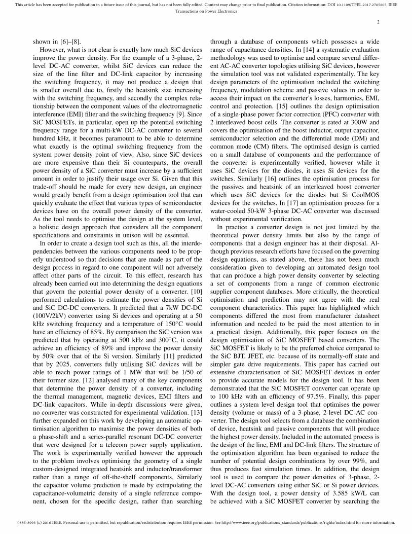
Fig. 1. Overview of the operational structure of the design optimisation tool
optimal switching frequency as compared to 1.426 kW/L fora Si IGBT converter.
The paper is organised as follows. Section II overviews thedesign tool, discussing its various component models throughway of a design example. Section III describes the operationof the optimisation algorithm and discusses how the algo-rithm’s structure can be altered to improve its computationalefficiency. Section IV outlines the experimental work carriedout on a 5 kW, 600 V DC-link SiC MOSFET based 3-phase inverter, in order to assess the accuracy of both themanufacturer data used in the design tool and the results ofthe design tool for the 2-level converter using SiC devices.Finally conclusions are drawn in section V.
II. DESIGN OPTIMISATION TOOL OVERVIEW
The design optimisation tool is composed of a set of inter-dependent component models, as shown in Fig. 1, each ofwhich are responsible for selecting and optimising a specificcomponent of the converter. The component models canbe categorised into one of three main areas; device lossmodelling, heatsink design and passive components design.This section discusses each of these areas by outlining thefundamental equations and selection criteria that govern themodels contained within them. To aid the discussion a designexample, based on the specifications and constraints givenin Table I, will be used to demonstrate the operation andoutputs of each of the component models. The objective ofthe example will be to minimise the overall volume, and byeffect the weight, of the converter.
TABLE IDESIGN EXAMPLE SPECIFICATIONS AND CONSTRAINTS
Specification ValueRated Power (Po) 5 kWDC-link voltage (Vdc) 600 VFundamental frequency (f0) 400 HzModulation index (M ) 0.9Power factor (PF ) 0.99Maximum junction temperature (Tj ) 125 CAmbient temperature (Ta) 40 CMaximum output current ripple (∆Io) 10% of IoMaximum DC-link voltage ripple (∆Vdc) 0.5% of VdcMinimum converter efficiency (η) 98%EMI limit standard DO-160E
A. Devices: Loss Modelling and Selection
The devices in the 3-phase, 2-level DC-AC converter con-tribute both conduction and switching losses. In [18] theconduction losses are split into those created when currentflows through the device’s channel and when it flows throughits anti-parallel or body diode. The optimisation carried outin this work will focus exclusively on SiC MOSFETs andtherefore the conduction losses in the channel and bodydiode, when the switching dead-time periods are ignored, arerespectively given by:
PQ =
(1
8+M
3πcos θ
)Rds(on)Id
2(1)
PD =
(1
8− M
3πcos θ
)RD(on)Id
2(2)
where Id = Peak MOSFET drain currentM = Modulation indexθ = Converter/output current phase angleRds(on) = MOSFET channel on resistanceRD(on) = Diode forward-biased resistance
For MOSFETs synchronous conduction is normally usedto reduce the conduction loss. This involves the channelconducting instead of the body diode when the current reversesthrough the MOSFET. In this case RD(on) in equation (2) isreplaced by Rds(on). The total conduction loss is then givenby:
Pcond = PQ + PD
=1
4Rds(on)Id
2(3)
The device switching losses are broken down into turn-on, turn-off, reverse-recovery and output capacitor losses.According to [19] the turn-on and turn-off losses are calculatedas follows:
Px = fsVdcVCC
(A0(x)
2+B0(x)
πId +
C0(x)
4Id
2)
(4)

0885-8993 (c) 2016 IEEE. Personal use is permitted, but republication/redistribution requires IEEE permission. See http://www.ieee.org/publications_standards/publications/rights/index.html for more information.
This article has been accepted for publication in a future issue of this journal, but has not been fully edited. Content may change prior to final publication. Citation information: DOI 10.1109/TPEL.2017.2705805, IEEETransactions on Power Electronics
4
where fs = Switching/carrier frequencyVCC = Test voltage of deviceA0(x)
B0(x)
C0(x)
=Device specific constants for xswitching losses
The constants A0(x), B0(x) and C0(x) can be taken from adevice’s datasheet switching energy, drain current relationship.Equation (4) can also be used to calculate the total reverserecovery losses. During the turn-off transition of a device’sbody diode, the reverse recovery effect will produce lossesin both the diode and the complementary device that issimultaneously turning on. The total losses in both the diodeand device can be obtained from equation (4) by setting A0(rr)
and C0(rr) to zero and then setting B0(rr) to:
B0(rr) =QrrVCC
ICC(5)
where Qrr = Reverse recovery chargeICC = Test current of device
Equation (4) then becomes:
Prr =fsVdcQrr
π
IdICC
(6)
The output capacitor of the MOSFET must discharge itsstored energy every switching cycle and thus has a switchingloss associated with it. This loss can be calculated by usingthe relationship between the device’s output capacitor storedenergy (Eoss) and its drain to source voltage (VDS) that isgiven graphically in the datasheet. The information can beapproximated by a quadratic and thus results in the followingformula:
Poss = fsVdcVCC
(AossVdc
2 +BossVdc)
(7)
whereAoss
Boss
=
Device specific constants forthe Eoss - VDS relationship
Summing all the various conduction and switching losseswill give the total loss for each device, which in turn can beused to determine the predicted efficiency of the converter foreach device. This is illustrated in Fig. 2 where the combinedconduction and switching losses of various devices from theCree C2M SiC MOSFET series have been used to calculatethe predicted converter efficiency over a range of switchingfrequencies for the design example specified in Table I. InFig. 2 the effect on efficiency due exclusively to conductionloss of the devices is given by the values at fs = 0 Hz,while the switching energy loss of each device correlates to thegradient of the curves where the larger the switching energythe steeper the gradient will be. From Fig. 2 it is clear thatdevices that have the lowest conduction losses also have thehighest switching energy loss. This trade-off of different losses
0 50 100 150 200 250 300 350 40092
93
94
95
96
97
98
99
100
fs (kHz)
Dev
ice
effi
cien
cy (
%)
C2M0025120D (90 A, 25 mΩ)C2M0040120D (60 A, 40 mΩ)C2M0080120D (36 A, 80 mΩ)C2M0160120D (19 A, 160 mΩ)C2M0280120D (10 A, 280 mΩ)
Fig. 2. Converter efficiency as a function of switching frequency when thetotal conduction and switching losses of various different Cree C2M seriesMOSFETs are considered
is a natural result of the size of the chip area of the device.As the chip area increases the on resistance (Rds(on) willdecrease and hence reduce the conduction losses. Howeverincreasing the area will also increase the output capacitance(Cds) which results in larger switching losses. Each devicehas a different chip area and thus the ratio of conduction toswitching losses is different for each device. Thus there areclearly defined switching frequency ranges where a specificdevice will have the smallest total loss. In practice, deviceselection is based first and foremost on whether the voltage andcurrent ratings of the device are greater than the voltages andcurrents it will be subject to in the converter. However for thecase were multiple devices meet the voltage and current ratingrequirements, these switching frequency ranges, based on thedevice losses, form the device selection criteria used by theoptimisation tool. Additionally at this stage of the process thedesign tool is able to determine which switching frequenciesproduce designs that meet the minimum efficiency requirementsince the power losses are dominated by the device switchinglosses.
Ultimately this method led the design tool to select theC2M0040120D device since it covers the range of frequenciesthat are most likely to be used by the optimisation toolin its final design. Despite the C2M0040120D possessing anominal current rating (60 A) well above the device’s RMScurrent (calculated at approximately 8.8 A), the device wasstill predicted to have the lowest combined conduction andswitching losses. Furthermore, the higher device rating isopportune for a couple of reasons. Firstly, the 60 A currentlimit is based on an operational temperature of 25 C, howeveras the converter is designed to operate at 125 C, temperaturede-rating of the current limit must be taken into account.According to the C2M0040120D datasheet, at 125 C thecurrent limit will be approximately 30 A. Secondly, 8.8 A isthe device’s RMS value, however in reality it will be subjectedto peak currents higher than this (calculated at 12.5A not
0885-8993 (c) 2016 IEEE. Personal use is permitted, but republication/redistribution requires IEEE permission. See http://www.ieee.org/publications_standards/publications/rights/index.html for more information.
This article has been accepted for publication in a future issue of this journal, but has not been fully edited. Content may change prior to final publication. Citation information: DOI 10.1109/TPEL.2017.2705805, IEEETransactions on Power Electronics
5
0 50 100 150 200 250 300 350 40090
92
94
96
98
100
fs (kHz)
Eff
icie
ncy
(%)
0 50 100 150 200 250 300 350 4000
150
300
450
600
750
Pow
er lo
ss (
W)
Simulation input = Datasheet information
Simulation input = Double pulse test data
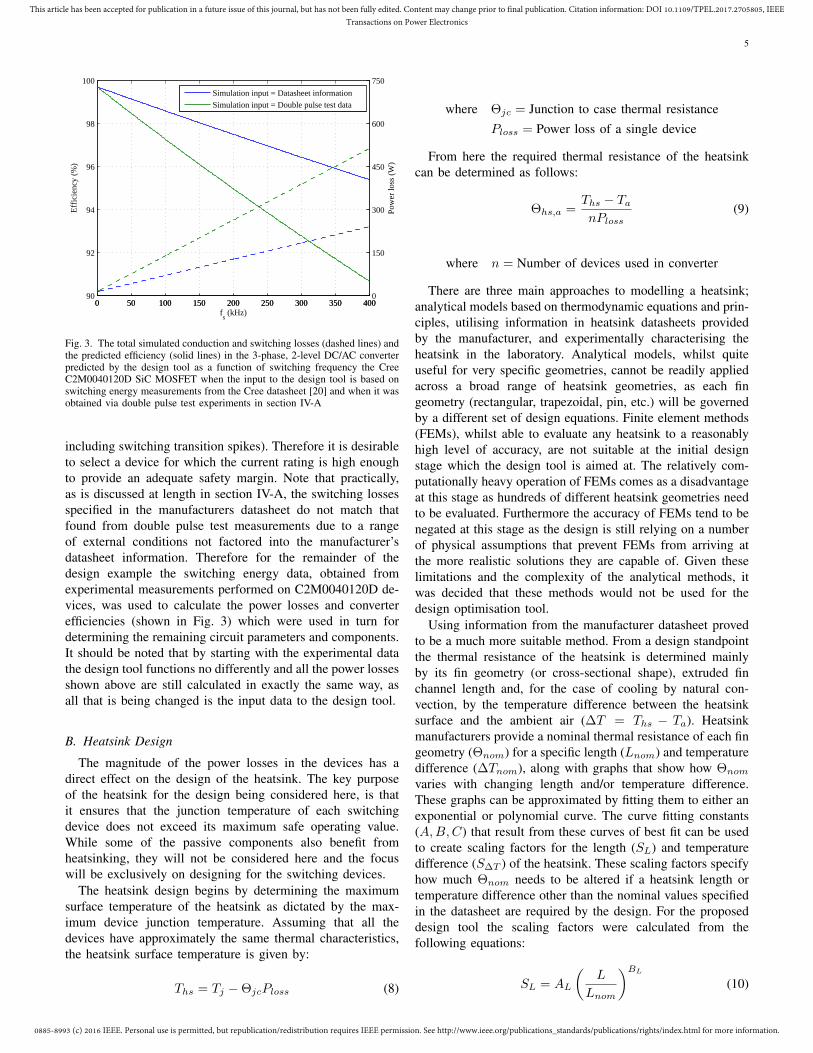
Fig. 3. The total simulated conduction and switching losses (dashed lines) andthe predicted efficiency (solid lines) in the 3-phase, 2-level DC/AC converterpredicted by the design tool as a function of switching frequency the CreeC2M0040120D SiC MOSFET when the input to the design tool is based onswitching energy measurements from the Cree datasheet [20] and when it wasobtained via double pulse test experiments in section IV-A
including switching transition spikes). Therefore it is desirableto select a device for which the current rating is high enoughto provide an adequate safety margin. Note that practically,as is discussed at length in section IV-A, the switching lossesspecified in the manufacturers datasheet do not match thatfound from double pulse test measurements due to a rangeof external conditions not factored into the manufacturer’sdatasheet information. Therefore for the remainder of thedesign example the switching energy data, obtained fromexperimental measurements performed on C2M0040120D de-vices, was used to calculate the power losses and converterefficiencies (shown in Fig. 3) which were used in turn fordetermining the remaining circuit parameters and components.It should be noted that by starting with the experimental datathe design tool functions no differently and all the power lossesshown above are still calculated in exactly the same way, asall that is being changed is the input data to the design tool.
B. Heatsink Design
The magnitude of the power losses in the devices has adirect effect on the design of the heatsink. The key purposeof the heatsink for the design being considered here, is thatit ensures that the junction temperature of each switchingdevice does not exceed its maximum safe operating value.While some of the passive components also benefit fromheatsinking, they will not be considered here and the focuswill be exclusively on designing for the switching devices.
The heatsink design begins by determining the maximumsurface temperature of the heatsink as dictated by the max-imum device junction temperature. Assuming that all thedevices have approximately the same thermal characteristics,the heatsink surface temperature is given by:
Ths = Tj −ΘjcPloss (8)
where Θjc = Junction to case thermal resistancePloss = Power loss of a single device
From here the required thermal resistance of the heatsinkcan be determined as follows:
Θhs,a =Ths − TanPloss
(9)
where n = Number of devices used in converter
There are three main approaches to modelling a heatsink;analytical models based on thermodynamic equations and prin-ciples, utilising information in heatsink datasheets providedby the manufacturer, and experimentally characterising theheatsink in the laboratory. Analytical models, whilst quiteuseful for very specific geometries, cannot be readily appliedacross a broad range of heatsink geometries, as each fingeometry (rectangular, trapezoidal, pin, etc.) will be governedby a different set of design equations. Finite element methods(FEMs), whilst able to evaluate any heatsink to a reasonablyhigh level of accuracy, are not suitable at the initial designstage which the design tool is aimed at. The relatively com-putationally heavy operation of FEMs comes as a disadvantageat this stage as hundreds of different heatsink geometries needto be evaluated. Furthermore the accuracy of FEMs tend to benegated at this stage as the design is still relying on a numberof physical assumptions that prevent FEMs from arriving atthe more realistic solutions they are capable of. Given theselimitations and the complexity of the analytical methods, itwas decided that these methods would not be used for thedesign optimisation tool.
Using information from the manufacturer datasheet provedto be a much more suitable method. From a design standpointthe thermal resistance of the heatsink is determined mainlyby its fin geometry (or cross-sectional shape), extruded finchannel length and, for the case of cooling by natural con-vection, by the temperature difference between the heatsinksurface and the ambient air (∆T = Ths − Ta). Heatsinkmanufacturers provide a nominal thermal resistance of each fingeometry (Θnom) for a specific length (Lnom) and temperaturedifference (∆Tnom), along with graphs that show how Θnom
varies with changing length and/or temperature difference.These graphs can be approximated by fitting them to either anexponential or polynomial curve. The curve fitting constants(A,B,C) that result from these curves of best fit can be usedto create scaling factors for the length (SL) and temperaturedifference (S∆T ) of the heatsink. These scaling factors specifyhow much Θnom needs to be altered if a heatsink length ortemperature difference other than the nominal values specifiedin the datasheet are required by the design. For the proposeddesign tool the scaling factors were calculated from thefollowing equations:
SL = AL
(L
Lnom
)BL
(10)

0885-8993 (c) 2016 IEEE. Personal use is permitted, but republication/redistribution requires IEEE permission. See http://www.ieee.org/publications_standards/publications/rights/index.html for more information.
This article has been accepted for publication in a future issue of this journal, but has not been fully edited. Content may change prior to final publication. Citation information: DOI 10.1109/TPEL.2017.2705805, IEEETransactions on Power Electronics
6
S∆T = A∆T
(∆T
∆Tnom
)2
+B∆T
(∆T
∆Tnom
)+ C∆T (11)
where L = Heatsink extrusion lengthLnom = Nominal extrusion length∆Tnom = Nominal temperature differenceAL/∆T
BL/∆T
CL/∆T
= Curve fitting constants
Using these scaling factors the actual thermal resistance forany combination of length and temperature difference is givenby the following equation:
Θsa = SLS∆T Θnom (12)
where Θnom = Nominal thermal resistance
Given that ∆T is already fixed, equations (10) to (12) canbe used to determine the required length of the heatsink whichin turn can be used to determine the heatsink mass and volumeenvelope.
Additionally, the heatsink design is also subject to variouslimiting constraints such as the maximum and minimumextrusion lengths. Manufacturers provide extrusions that arecut to a stock length which a designer may cut down to ashorter length. Longer extrusions can be acquired by makinga custom order, however since the optimisation tool presentedhere focuses on utilising readily available components, themaximum extrusion length will be restricted to the stocklength provided by the manufacturer. The minimum extrusionlength is constrained by the minimum length required to fit thefootprints of all the devices onto the heatsink. If we considerthat n devices of the dimensions Lm ×Wm need to fit atopthe heatsink then these devices can be arranged in 2N wayswhere N is the number of factors of n including 1 and itself.The factor of 2 is a result of the fact that as long as Lm 6= Wm
then the device can be orientated either with its length orwidth aligned with the front edge of the heatsink. Fig. 4 showsall the possible arrangements, and how it affects the overallfootprint length and width, for the case of n = 4. The layoutarrangement that will be selected by the optimisation tool willby the one that has the shortest overall footprint length (LFP )while also ensuring that the overall footprint width is less thanthe heatsink width (WFP < WHS).
Returning to the design example, Fig. 5 shows the heatsinkextrusion lengths and volume envelopes for four differ-ent heatsink fin geometries from Aavid Thermalloy [21].The power losses were calculated for an inverter utilisingC2M0040120D devices as in accord with the results shownin Fig. 3. The solid lines display the calculated heatsinklength and volume with the minimum and maximum lengthconstraints included, while the dotted lines show the length and
LFP
LFP
LFP
LFP
LFP
LFP
WFP
WFP
WFP
WFP
Wm
Lm
Individual Device
Footprint
Potential Layout
Footprints
Fig. 4. Device footprint layouts, and their corresponding dimensions, for 4devices
volume that could be achieved if there were no length con-straints. The minimum length constraints produce the horizon-tal portions of the curves that occur at the lowest frequenciesin Fig. 5. They show that below a certain switching frequencythe minimum length, and subsequently the minimum volume,has been reached and no shorter lengths can be achieved atlower frequencies. The maximum length constraints producethe vertical portions of the curves in Fig. 5. In this case assoon as the switching frequency increases to a value where itproduces the maximum length of a particular extrusion (suchas 150 mm for the 0K267), all switching frequencies greaterthan this value will set the length to infinity (or a suitablyhigh value) thus creating the vertical portions of the curve.This ensures that the design tool will not be able to selectthat particular extrusion at these higher switching frequencies.Focusing on the 0K267 heatsink in Fig. 5, despite it being thelongest in length, its compact profile produces the smallestvolume envelope. However, given that its maximum length isonly 150 mm it is limited to switching frequencies below 52kHz, after which 000EK* becomes the best option.
Finally it should be noted that while the datasheet basedmethod is useful for the initial design stage, just like for theanalytical methods, it is limited in its accuracy due to it lackingparticular pieces of realistic information. As a result the designhad to be supplemented with an experimental characterisationwhich will be discussed in section IV-B.
C. Passive Components Design
The passive components that the converter is comprised ofinclude a DC link capacitor at the input, and a line and EMIfilter at the output. The purpose of the DC link filter is tolimit the input voltage ripple of the converter while the linefilter is used to limit the output current ripple. The purposeof the EMI filter is to limit the amount of both the conducteddifferential mode (DM) and common mode (CM) noise of theconverter. Similar to the heatsink design, the optimisation tool

0885-8993 (c) 2016 IEEE. Personal use is permitted, but republication/redistribution requires IEEE permission. See http://www.ieee.org/publications_standards/publications/rights/index.html for more information.
This article has been accepted for publication in a future issue of this journal, but has not been fully edited. Content may change prior to final publication. Citation information: DOI 10.1109/TPEL.2017.2705805, IEEETransactions on Power Electronics
7
(a)
0 50 100 150 200 250 3000
50
100
150
200
250
300
350
fs (kHz)
LH
S (m
m)
000EK*000EM0K2670K278
(b)
0 50 100 150 200 250 3000
500
1000
1500
2000
2500
3000
3500
4000
fs (kHz)
VH
S (cm
2 )
000EK*000EM0K2670K278
(c)
Fig. 5. Examples of heatsink fin geometries analysed by the optimisation tool: (a) Extrusion cross-section dimensions, (b) Minimum required extrusion lengthand (c) Minimum volume envelope. Figures (b) and (c) are created assuming C2M0040120D devices have been selected. Dotted lines indicate the length ifno maximum or minimum limits are applied to the extrusion length
assesses a range of switching frequencies to determine whichcombination of components and switching frequency producesthe design with the smallest total volume.
When selecting the DC-link capacitor, two main objectivesmust be taken into consideration. Firstly the capacitance mustbe large enough to meet the voltage ripple requirement ofthe inverter. Secondly, the capacitor must be able to sustainthe ripple current that the circuit will subject it to otherwiseit may overheat and exceed its temperature rating. Appropri-ate capacitor types for the DC-link filter include aluminiumelectrolytic capacitors and metallised polypropylene film ca-pacitors. Electrolytic capacitors exhibit high capacitance perunit volume but possess a relatively high equivalent seriesresistance (ESR) and thus are limited by the ripple currentrequirements. Metallised polypropylene film capacitors exhibitlow ESR and low capacitance per unit volume and thus arelimited by the voltage ripple requirement [22]. As a resultthe proposed design tool implements different capacitor sizing
methods depending on which type of capacitor and thus whichmajor ripple limitation needs to be considered.
In order to correctly size an electrolytic capacitor so thatit adheres to the ripple current requirement, one must firstcalculate the RMS value of the current flowing through thecapacitor. This is done according to the following equation[23]:
IC(rms) = Irms
√√√√2M
(√3
4π+ cos2 θ
(√3
π− 9
16M
))(13)
where Irms = RMS output phase current
As IC(rms) is fundamentally an AC current it can becompared with the ripple current ratings (Irip) given in theelectrolytic datasheets. As ripple currents are typically definedfor an operational frequency of 120 Hz, an appropriate ripple

0885-8993 (c) 2016 IEEE. Personal use is permitted, but republication/redistribution requires IEEE permission. See http://www.ieee.org/publications_standards/publications/rights/index.html for more information.
This article has been accepted for publication in a future issue of this journal, but has not been fully edited. Content may change prior to final publication. Citation information: DOI 10.1109/TPEL.2017.2705805, IEEETransactions on Power Electronics
8
n
LΔI LDM LCM
CDM CCM
RL
Cdc
+
Vdc−
Fig. 6. Experimental setup of filter components of the 2-level, 3-phase DC/AC converter
current multiplier must be selected from the datasheet toensure that the ripple current rating is scaled for use with thekHz frequency range that the design tool will operate within.With this information the design tool can select a capacitor (orcapacitor combination) that has a higher ripple current ratingthen the capacitor current i.e. Irip > IC(rms).
For a metallised polypropylene film capacitor whose designis based primarily on the voltage ripple requirement (∆V ), itscapacitance, which will be the main dictator of its physicalsize, can be approximately calculated according to the follow-ing equation [24]:
Cdc =MIrms
16∆V fs
√√√√(6− 96√
3
5πM + 9
2M2
)cos2 θ +
8√
3
5πM
(14)At the output of each phase is an LC network that combines
to form the line and EMI filters. The filter consists of threemain stages, as shown in Fig. 6, which is representative forgrid-tie and inverter applications (other filter types can alsobe considered). The first stage is the line filter which consistsof a single inductor on each phase (L∆I ). The second is theDM filter which consists of capacitors (CDM ) and additionalinductors (LDM ) that when combined with L∆I creates anLCL network that forms the full DM filter. The final stageis the CM filter which consists of capacitors (CCM ) and a 3-phase CM choke (LCM ) that when combined with L∆I createsan LCL network that forms the full CM filter. The optimisationtool designs each of these stages in turn, beginning with theline filter and adding on the DM and CM filters afterwards.
The size of the line filter’s inductance is determined bythe design constraint governing the maximum allowable ripplecurrent. This results in a single inductance value for eachpossible switching frequency. The relationship between themaximum ripple current and line inductance (for low to mid-range switching frequencies) is approximated by the followingequation [25]:
∆I =VdcMTs
4√
3L∆I
(15)
where Ts = Switching/carrier period
Both the DM and CM components of the EMI filter aredesigned so that they conform to the L, M and H categoriesof the DO-160E standard [26]. In order to achieve this, the DMand CM harmonics are calculated for the frequencies specifiedby the standard. If it is assumed that naturally sampled, sine-triangle modulation is used to control the converter, thenaccording to [27] the major harmonics occur at frequenciesof f(m,n) = mfs + nf0, where m and n are integer values.These major harmonics can be decomposed into their DM andCM voltage components by using equations (16a) and (16b)[28]. Example results for these equations are shown in Fig. 7which displays the DM and CM voltage harmonics for thecase where the switching frequency is 63 kHz and all otherparameters are as given in Table I.
∣∣VDM(m,n)
∣∣ =
∣∣∣∣4Vdc√3πX(m,n) sin
(nπ
3
)∣∣∣∣ (16a)

0885-8993 (c) 2016 IEEE. Personal use is permitted, but republication/redistribution requires IEEE permission. See http://www.ieee.org/publications_standards/publications/rights/index.html for more information.
This article has been accepted for publication in a future issue of this journal, but has not been fully edited. Content may change prior to final publication. Citation information: DOI 10.1109/TPEL.2017.2705805, IEEETransactions on Power Electronics
9
50 100 150 200 250 3000
10
20
30
40
50
60
70
80
90
Frequency (kHz)
VD
M a
mpl
itude
(V
)
(a)
50 100 150 200 250 3000
50
100
150
200
250
Frequency (kHz)
VC
M a
mpl
itude
(V
)
(b)
Fig. 7. Frequency spectra of the (a) DM voltage harmonics and (b) CM voltage harmonics for fs = 63 kHz, f0 = 400 Hz, Vdc = 600 V and M = 0.9
L1 L2
Cf
+
VDM
−
Vc
Io
RL
(a)
L1 L2
Cf
+
VCM
−
Vc
Io
RL
Cg
(b)
L1 L2
Cf
+
Vi
−
Vc
Io
(c)
Fig. 8. Single-phase LCL filter models for the (a) DM EMI filter, (b) CM EMI filter and (c) DM and CM filter with a short-circuit load
∣∣VCM(m,n)
∣∣ =
∣∣∣∣2Vdc3πX(m,n)
(1 + 2 cos
(n
2π
3
))∣∣∣∣ (16b)
where X(m,n) =1
mJn
(mπ
2M)
sin(
(m+ n)π
2
)In order to adhere to the design’s specifications, the opti-
misation tool needs to ensure that the load current harmonicsof each phase are below the limit specified by the DO-160Estandard (Ilim). As mentioned above, the DM and CM filterswere modelled as LCL filters each connected to an appropriateload. For the DM filter this is just a resistance (RL) whereasfor the CM filter it was a resistance plus a parasitic capacitanceto ground (Cg) as shown in Fig. 8a and 8b respectively.Typically in either case the impedance of the filter inductorswill be much higher than the load resistance (i.e. ωL > RL),and thus the load can be treated as a short circuit (RL = 0).This assumption is beneficial during the design process as itcorresponds to the worst case scenario when the load currentis at its maximum. With this in mind it is therefore useful toreplace Cg with a short-circuit, in the case of the CM filter, toensure that the worst case scenario is designed for. Thereforeboth the DM and CM models simplify to that shown in Fig. 8cand the resulting LCL filter will produce the following transferfunction:
Vi(jω(m,n)
)Io(jω(m,n)
) = jω(m,n)
(L1 + L2 − ω(m,n)
2L1L2Cf
)(17)
From (17) it can be seen that the angular resonant frequencyof an LCL filter is given by ωres =
√L1+L2
L1L2Cf. Substituting
this into (17) produces:
∣∣∣∣∣Vi(jω(m,n)
)Io(jω(m,n)
) ∣∣∣∣∣ = ω(m,n) (L1 + L2)
∣∣ω(m,n)2 − ωres
2∣∣
ωres2
(18)
Equation (18) shows that the filter attenuation at a particularfrequency is dependent on the total filter inductance (L1 +L2)and the resonant frequency. The optimisation tool specifies thatL1 be the line inductance, as calculated from (15). Basingthe value of L1 on the ripple current requirement may resultin a slightly larger filter volume than if L1 was optimisedsimultaneously with L2 and Cf , however doing so doesn’thave a detrimental affect on the overall power density, sincethe EMI requirements are typically much stricter than thecurrent ripple requirements of an application. For exampleif the current ripple is allowed to be larger than 10% (as isthe case in this design example), then the size of the lineinductor would decrease. However, the size of all the EMIfilter components would need to increase in order to meetthe EMI requirements and thus the overall volume wouldnot be significantly reduced. Furthermore, basing L1 on onlyripple current greatly improves the computation time of thedesign tool as it only has to simultaneously search throughtwo component databases (L2 and Cf ) rather than three, and
0885-8993 (c) 2016 IEEE. Personal use is permitted, but republication/redistribution requires IEEE permission. See http://www.ieee.org/publications_standards/publications/rights/index.html for more information.
This article has been accepted for publication in a future issue of this journal, but has not been fully edited. Content may change prior to final publication. Citation information: DOI 10.1109/TPEL.2017.2705805, IEEETransactions on Power Electronics
10
thus was considered to be the better design methodology forthe optimisation tool.
Next the design tool specifies a range of inductances thatL2 is allowed to take. For each potential value of L2 theoptimisation tool calculates the resonant frequency of thefilter, that will be required to achieve the desired attenuation,according to the following equation:
ωres = ω(m,n)
√ω(m,n) (L1 + L2)
∣∣Io(m,n)
∣∣ω(m,n) (L1 + L2)
∣∣Io(m,n)
∣∣+∣∣Vi(m,n)
∣∣(19)
From here the range of values of L2 and its correspondingrange of resonant frequencies are translated into a range ofvalues for the capacitance Cf . This completes a range ofinductance-capacitance (L − C) pairs that will comprise theDM and CM parts of the EMI filter. For the DM section of thefilter, the optimisation tool substitutes the following values intoequation (19): Vi = VDM , Io = Ilim, L1 = L∆I , L2 = LDM ,Cf = CDM . For the CM section it substitutes the following:Vi = VCM , Io = Ilim, L1 = 1
3L∆I , L2 = LCM , Cf = CCM .At this point in the optimisation process, each and every
switching frequency will yield a single L or C value for theline inductor and DC-link capacitor, and a range of L − Cpairs for the DM and CM portions of the EMI filter. For thenext stage of the optimisation process, the tool will convertall the L and C values into real physical parts by designingand selecting each component from a suitable subset of parts.The line and DM inductors are constructed from gapped ferritecores where the optimisation tool determines the core size, gaplength, winding diameter and number of turns. The diameter ofthe windings are selected based on the desired current densityof the wire (Jrms). The core selection was based on the area-product method outlined in [29] which states that the core sizemust satisfy the following inequality:
AwAcore >LIIrms
KuJrmsB(20)
where Aw = Winding window areaAcore = Core area
I = Peak inductor currentIrms = RMS inductor currentKu = Window utilisation factor
B = Maximum allowable flux density
Once the core has been selected the number of turns andthe gap length are calculated according to the following:
n =LI
BAcore
(21)
lg =µn2Acore
L(22)
where µ = Core permeability
0 50 100 150 200 250 300 350 4000
50
100
150
200
250
300
350
400
450
500
fs (kHz)
Vol
ume
(cm
3 )
L
DM
CDM
Total DM
Fig. 9. Optimised volume of the differential mode (DM) filter components(excluding the line inductor) as a function of switching frequency
The optimisation tool constructs the CM inductor from atoroidal coil. The winding diameter is, once more, set by thedesired current density. Once selected, the winding diameteris used to determine the maximum number of turns, andhence the maximum inductance, that each specific core in thecomponent database is capable of producing. The EMI filter iscompleted by the optimisation tool selecting film suppressioncapacitors for CDM and CCM . For safety reasons class X1capacitors were used in the DM filter while class Y2 were usedin the CM one. The selection process involves the optimisationtool assessing each capacitor in the component database bydetermining the number that would need to be paralleledto meet the capacitance requirement and then selecting thatwhich has the lowest overall volume. The DC link capacitoris selected via the same method however it is selected from adatabase of film and/or electrolytic capacitors suitable for DCfiltering.
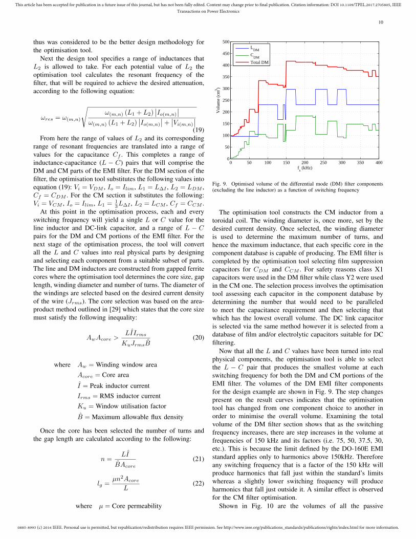
Now that all the L and C values have been turned into realphysical components, the optimisation tool is able to selectthe L − C pair that produces the smallest volume at eachswitching frequency for both the DM and CM portions of theEMI filter. The volumes of the DM EMI filter componentsfor the design example are shown in Fig. 9. The step changespresent on the result curves indicates that the optimisationtool has changed from one component choice to another inorder to minimise the overall volume. Examining the totalvolume of the DM filter section shows that as the switchingfrequency increases, there are step increases in the volume atfrequencies of 150 kHz and its factors (i.e. 75, 50, 37.5, 30,etc.). This is because the limit defined by the DO-160E EMIstandard applies only to harmonics above 150kHz. Thereforeany switching frequency that is a factor of the 150 kHz willproduce harmonics that fall just within the standard’s limitswhereas a slightly lower switching frequency will produceharmonics that fall just outside it. A similar effect is observedfor the CM filter optimisation.
Shown in Fig. 10 are the volumes of all the passive

0885-8993 (c) 2016 IEEE. Personal use is permitted, but republication/redistribution requires IEEE permission. See http://www.ieee.org/publications_standards/publications/rights/index.html for more information.
This article has been accepted for publication in a future issue of this journal, but has not been fully edited. Content may change prior to final publication. Citation information: DOI 10.1109/TPEL.2017.2705805, IEEETransactions on Power Electronics
11
0 50 100 150 200 250 300 350 4000
200
400
600
800
1000
1200
1400
1600
fs (kHz)
Vol
ume
(cm
3 )
L∆I
DMCMC
dc
Total
Fig. 10. Optimised total volume of the all the passive components as afunction of switching frequency. Note that “DM” refers to the combinedvolume of LDM and CDM , and “CM” refers to the combined volume ofLCM and CCM
components and their combined overall volume as a functionof the switching frequency. The DM and CM filter volumesfollow the patterns described above. Since only a finite numberof components can be selected from the database, not everyintermediate volume value can be obtained and thus the resultsplot as a step-based discrete function. This is most clearlyseen with the volume of the line inductor where each stepon the curve represents a distinct inductor core and bobbin. Ifevery intermediate inductor volume could be achieved then thevolume curve would be approximately inversely proportionalto the switching frequency. However, since there are a finitenumber of cores and bobbins, optimising over a range ofswitching frequencies results in volume steps that follow thistrend but don’t match it exactly. For example the step startingat 63 kHz and finishing at 95 kHz represents the ETD59/31/22core and bobbin where the number of turns decreases as thefrequency increases. At 63 kHz the number of turns completelyfills the winding window however this will not change theoverall volume envelope as the windings will all be containedwithin the space defined by the bobbin. Therefore if theswitching frequency was to be made lower than 63 kHz then alarger core would be required. Since the ETD59 core was thelargest one in the database, the design tool sets the volume tovirtual infinity for all switching frequencies below 63 kHz soto indicate that no core will meet the design specifications atthese frequencies. At 96 kHz the design tool is able to identitya smaller core and bobbin, that when its winding window iscompletely filled, produces the required amount of inductance.Thus the design tool selects this smaller volume core for allfurther switching frequencies until the process repeats and aneven smaller core can achieve the required inductance.
D. Overall Converter Results
To finish the design process the optimisation tool calculatesthe total converter volume by adding the heatsink and passive
0 50 100 150 200 250 300 350 4000
500
1000
1500
2000
2500
3000
3500
4000
4500
5000
63 kHz, 1427 cm3
fs (kHz)
Vol
ume
(cm
3 )
HeatsinkPassivesTotal
Fig. 11. Optimised total converter volume (i.e combined heatsink and passivecomponents volume) as a function of the switching frequency with a markerindictating the absolute minimum volume and the optimal frequency at whichit occurs
component volumes at each potential switching frequency,as is shown for the design example in Fig. 11. It can beseen that as the switching frequency increases the heatsinkvolume increases while the volume of the passive componentstends to decreases, however in this case the rate of increaseof the heatsink is much greater than any decrease in thepassives. With this final piece of information the optimisationtool is able select the converter design that produces thesmallest total volume, which for the design example is 1427.19cm3 produced at a switching frequency of 63 kHz. The fullcomponent details of the optimal design for this example aregiven in Table II while a breakdown of the contribution of eachcomponent to the total converter volume is shown in Fig. 12a.For the sake of comparison, the optimisation tool was used todesign a converter with the same specifications except this timeit was to use Si IGBT devices. The design produced by the toolis also shown in Table II, side by side with the SiC MOSFETdesign, and a volume breakdown of the converter is shown inFig. 12c. As can be seen the switching frequency is reducedto 6 kHz leading to a significant increase in the volume ofthe passive components, especially the line inductor. The endresult is that the power density of the SiC MOSFET design is159.4% higher than the Si IGBT one. It should also be notedthat the efficiency of the Si IGBT design is only 96% as nocomponents in the database could be combined to achieve thedesired 98% efficiency and thus a compromise had to be madeso that a valid design could be presented.
III. OPTIMISATION ALGORITHM IMPLEMENTATION
A simplified operational flow diagram of the optimisationtool is shown in Fig. 13. The process begins by the userdefining the specifications (e.g. output voltage, power rat-ing), constraints (e.g. minimum converter efficiency, maximumcomponent temperatures) and objectives (e.g. minimise thevolume). The algorithm then combines all the suitable itemsin the component databases with all the potential converter

0885-8993 (c) 2016 IEEE. Personal use is permitted, but republication/redistribution requires IEEE permission. See http://www.ieee.org/publications_standards/publications/rights/index.html for more information.
This article has been accepted for publication in a future issue of this journal, but has not been fully edited. Content may change prior to final publication. Citation information: DOI 10.1109/TPEL.2017.2705805, IEEETransactions on Power Electronics
12
658.3 cm3
(46%)
94.41 cm3
(7%)
117.5 cm3
(8%)
23.7 cm3 (2%)
39.5 cm3 (3%)
12 cm3 (< 1%)
481.7 cm3
(34%)
L∆I
LDM
CDM
LCM
CCM
Cdc
Heatsink
(a) Volume optimised SiC converter
1.294 kg(59%)
0.1347 kg(6%)
0.1218 kg(6%)
0.07167 kg (3%)
0.04207 kg (2%)0.01278 kg (< 1%)
0.5159 kg(24%)
(b) Mass optimised SiC converter
2730 cm3
(74%)
13.33 cm3 (< 1%)
27.81 cm3 (< 1%)
8.921 cm3 (< 1%)
3.564 cm3 (< 1%)
77.63 cm3 (2%)
840.3 cm3
(23%)
L∆I
LDM
CDM
LCM
CCM
Cdc
Heatsink
(c) Volume optimised Si converter
6.371 kg(78%)
0.02934 kg (< 1%)
0.0369 kg (< 1%)
0.004834 kg (< 1%)
0.02103 kg (< 1%)
0.05732 kg (< 1%)
1.634 kg(20%)
(d) Mass optimised Si converter
Fig. 12. Contribution of each component in a SiC MOSFET or Si IGBT based converter that has been optimised for either volume or mass
operating conditions (e.g. the range of allowable switchingfrequencies) to create every possible design within the solu-tion space. Each design is checked to see if it satisfies theconstraints and, if successful, will have its objective valuecalculated, referred to as the design’s cost (e.g. the design’stotal volume or mass). If the calculated cost of the currentdesign is less than the cost of all the other designs that havebeen examined thus far, then the optimisation algorithm willstore the current design as the best design and all the remainingdesigns will be compared against it until a design with an evenlower cost is found. Upon completion the algorithm will haveiterated through all the possible designs and selected the onethat has the lowest cost as the optimal design. This methodis effective in finding the optimal design however it is veryinefficient as it must check through every possible design inthe solution space in order to do so.
The reason that the method described above is inefficientis because it is effectively a nested loop structure where eachlevel of the structure is occupied by a single design variableset. An example of this structure for 4 design variable sets isshown in Fig. 14a. In this case the total number of designsthat will need assessing is equal to Na × Nb × Nc × Nd. Itcan be seen that as the number of design variables increases,the number of designs grows exponentially. In order to reduce
the number of designs, and hence improve the computationalefficiency, the algorithm has been structured so that it exploitsthe interdependency relationships of the design variables. Thismethod identifies whether or not one variable is directly de-pendent on another variable or if they are indirectly connectedthrough a chain of variables. Identifying variables by thismanner results in a structure where dependent variables branchoff from each other. The variables that has the most dependentvariables branching from it forms the underlying outer loopof the design tool algorithm while the other variables formthe various nested loop levels. The overall effect is that thenumber of nested loop levels is reduced. An example of thisis given in Fig. 14b where the same 4 design variables shownin Fig. 14a have been reused. In this case variable B branchesfrom variable A while variables C and D branch from A ratherthan B as was the case in Fig. 14a. Therefore the total numberof designs is now given by Na (Nb +NcNd).
This type of branching structure shown in Fig. 14b wasapplied to the design optimisation tool by examining itsoperational structure shown in Fig. 1. The structure links thevarious design specifications, constraints and objectives feedinto the tool by the user, to the various component modelsand selection procedures controlled by the tool’s algorithm.At the highest level the optimisation tool makes selections

0885-8993 (c) 2016 IEEE. Personal use is permitted, but republication/redistribution requires IEEE permission. See http://www.ieee.org/publications_standards/publications/rights/index.html for more information.
This article has been accepted for publication in a future issue of this journal, but has not been fully edited. Content may change prior to final publication. Citation information: DOI 10.1109/TPEL.2017.2705805, IEEETransactions on Power Electronics
13
Combine solution space variables to create
every possible design, S = s1, s2, ... sN
Compute component values and
operational parameters for design ‘sn’
Constraints
satisfied?
Compute cost c(sn)
c(sn) <
c(s*)?
c(s*) = c(sn), s* = sn
START
END
n = N?
n = n + 1
No
No
No
n = 1
Yes
Yes
Yes
Define specifications
Initiate c(s*) = ∞ , s* =
Define solution space
Define constraints
Define objective
‘USER’
Fig. 13. Operational flow diagram of the optimisation tool [30]
A = a1,…,aNa
B = b1,…,bNb
C = c1,…,cNc
D = d1,…,dNd
(a)
A = a1,…,aNa
C = c1,…,cNc
B = b1,…,bNb
D = d1,…,dNd
(b)
Switching frequency
DC-link capacitor
Device
Line inductor
Heatsink
EMI filter
(c)
Fig. 14. Design variable arrangement structures; (a) Nested loop structure, (b)Branching variable structure, (c) 3-phase DC/AC inverter design tool structure
TABLE IIDESIGN EXAMPLE OPTIMISED COMPONENT DETAILS
Design parameter SiC MOSFET Si IGBTVolume 1427.19 cm3 3701.96 cm3
Switching frequency 63 kHz 6 kHzDevice C2M0040120D FGW15N120VDHeatsink 000EK* 000EK*• Length 40.15 mm 70.03 mmL∆I 964.7 µH 10.417 mH• Core ETD59/31/22 E100/60/28• # turns 71 375• Gap length 2.4 mm 12.5 mm• Wire size 1.8 mm 1.8 mmLDM 50 µH 5 µH• Core ETD29/16/10 E19/8/5• # turns 18 6• Gap length 0.6 mm 0.2 mm• Wire size 1.8 mm 1.8 mmCDM 1.76 µF 0.33 µF• Type 474R32201A12 BFC23381X334• # in parallel 8 1LCM 646.38 µH 188.19 µH• Core TX36/23/15-3E5 R25.3/14.8/10-T37• # turns 9 6• Wire size 1.8 mm 1.8 mmCCM 0.44 µF 0.015 µF• Type B32024A3224M B32022A3153M• # in parallel 2 1Cdc 3 µF 30 µF• Type MKP1848530094K2 C4AEOBW5300A3MJ• # in parallel 1 1
in regards to the operating conditions of converter such asthe switching frequency, which is then passed down into thecomponent models in order to design and select all the variouscomponents such as the switching devices, the heatsink and thepassive components. The selected components are then passedback up the structure to be measured against the specifications,constraints and objectives and help inform the tool’s decisionas to what the optimal operating conditions should be. FromFig. 1 it can be seen that the devices and heatsink selectionform one branch off of the operating conditions and switchingfrequency, while the passive component selection proceduresform a separate branch. Therefore these sections of the algo-rithm can make use of the branching variable structure in theway shown in Fig. 14c where the switching frequency formsthe outer loop of the algorithm from which the other variablesbranch off from.
For the design example discussed in section II the com-ponent database and circuit parameters that the tool wasable to select and form potential designs from is given inTable III. Without restructuring, the algorithm is requiredto assess approximately 2.2 × 10¹² designs. By comparison,using the independent variable separated structure illustratedin Fig. 14b, the number of designs is reduced to 224,822 whichis a reduction of over 99.9%.

0885-8993 (c) 2016 IEEE. Personal use is permitted, but republication/redistribution requires IEEE permission. See http://www.ieee.org/publications_standards/publications/rights/index.html for more information.
This article has been accepted for publication in a future issue of this journal, but has not been fully edited. Content may change prior to final publication. Citation information: DOI 10.1109/TPEL.2017.2705805, IEEETransactions on Power Electronics
14
TABLE IIIDESIGN EXAMPLE COMPONENT DATABASE AND CIRCUIT PARAMETERS
Design parameter ValuesDevice type Cree C2M MOSFETs (5 in total)Switching frequency 10, 11, , 400 kHzLine and DM inductor Ferroxcube gapped double ETD cores
core type (7 in total)CM inductor core type TDK/EPCOS & Ferroxcube toroids
(44 in total)DM capacitor type Kemet & Vishay X1 class film (21 in total)CM capacitor type Kemet, TDK & Vishay Y2 class film
(68 in total)DC link capacitor type AVX, Kemet & Vishay DC film (36 in total)Heatsink types Aavid thermalloy (14 in total)
IV. DESIGN OPTIMISATION TOOL EXPERIMENTALVERIFICATION
In order to fully assess the design optimisation tool, it isnecessary to first determine whether or not the componentdata used by the tool matches that of an actual experimentalconverter. This section first focuses on the two areas wherethe greatest discrepancy between component manufacturerdata and actual converter measurements usually occur; deviceswitching losses and heatsink thermal resistance. It then in-vestigates the performance of a converter built according tothe results of the design example given in Table II. Throughexperiments carried out on the converter, the device loss modeland the output filter design model of the optimisation tool areevaluated.
A. Device Switching Loss Measurement
The switching energy loss of a converter is affected bynot only the inherent switching energy of the device itself,but also by the surrounding circuitry in which the deviceis placed. The switching energy (Eon, Eoff ) specified ina manufacturer’s datasheet is based on a clamped inductiveswitching test that inserts the device under test (DUT) into anevaluation board. The board itself consists of a single phaseleg where the DUT is usually paired with a Schottky diodesince a Schottky has low switching losses and no reverserecovery. External components such as gate drive circuitsand load inductances are added externally so that variousdifferent operating conditions can be tested. Consequently, theswitching energy results produced are specific to componentvalues, board layout and the operating conditions used.
The uniqueness of the manufacturer’s results becomes prob-lematic when trying to apply them to a converter design forseveral reasons. Firstly the components used in the actual 3-phase converter will be different and thus change the switchingdynamics of the system. The phase leg typically consistsof two SiC MOSFETs placed in both the upper and lowerpositions, one of which is the DUT, as the current in the phaseleg must be bi-directional and thus changes the switchingwaveforms that the DUT is subject to. The gate drive circuitrywill also be different to that used in the manufacturer’s setupin order to meet the speed, power and stability requirements
Q1
C2M0040120D
Q2
C2M0040120D
1.31mH
120μF, 900V
MKP1848
600V
EA-PS 8600-70
19Ω
Gate drive
boardDUT
Fig. 15. Schematic of the double pulse test setup
Fig. 16. Power board, devices and gate drivers of a 3-phase, 2-level DC-ACconverter created by the design optimisation tool. A single phase leg was usedfor double pulse test measurements
of the actual converter. As a result the gate drive producessignals that might transition faster or slower, or even beshaped differently altogether to the signals that produced themanufacturer’s results. Secondly, the PCB layout of the actualconverter will be different to the manufacturer’s setup andhence will be subject to different parasitic components thatwill change the shape of the turn-on and turn-off transitions.This is of particular importance for SiC devices since smallchanges in the layout can have significant effects on theswitching energy requirement of the devices, much more sothan is the case for Si devices.
For these reasons, double pulse tests (DPTs) were carriedout on the converter created by the optimisation design tool, todetermine the real switching losses of the chosen SiC devices.A simplified schematic of the double pulse setup is shownin Fig. 15 along with the various component values used inthe double pulse test. Fig. 16 shows the converter’s powerboard containing the 3 phase legs with their upper and lowerdevices, of which a single phase leg was used for the DPTs.Fig. 17 shows the turn-on and turn-off transitions capturedduring the DPTs for load currents of 10 A, 25 A and 40 Awhere the gate resistance used was 24Ω. The current overshootpresent on all the turn-on transitions (Fig. 17a, 17b and 17c) isproduced in part by the high dv/dt experienced by the outputcapacitance of the devices and in part by the reverse recoveryeffect of the complementary device’s body diode. The turn on

0885-8993 (c) 2016 IEEE. Personal use is permitted, but republication/redistribution requires IEEE permission. See http://www.ieee.org/publications_standards/publications/rights/index.html for more information.
This article has been accepted for publication in a future issue of this journal, but has not been fully edited. Content may change prior to final publication. Citation information: DOI 10.1109/TPEL.2017.2705805, IEEETransactions on Power Electronics
15
Time (ns)
Vol
tage
(V
)
0 200 400 600 800−100
0
100
200
300
400
500
600
700
0 200 400 600 800−2.5
0
2.5
5
7.5
10
12.5
15
17.5
Cur
rent
(A
)
(a)
Time (ns)
Vol
tage
(V
)
0 200 400 600 800−100
0
100
200
300
400
500
600
700
0 200 400 600 800−5
0
5
10
15
20
25
30
35
Cur
rent
(A
)
(b)
Time (ns)
Vol
tage
(V
)
0 200 400 600 800−100
0
100
200
300
400
500
600
0 200 400 600 800−10
0
10
20
30
40
50
60
Cur
rent
(A
)
(c)
Time (ns)
Vol
tage
(V
)
0 200 400 600 800−100
0
100
200
300
400
500
600
700
0 200 400 600 800−2
0
2
4
6
8
10
12
14C
urre
nt (
A)
(d)
Time (ns)
Vol
tage
(V
)
0 200 400 600 800−100
0
100
200
300
400
500
600
700
0 200 400 600 800−5
0
5
10
15
20
25
30
35
Cur
rent
(A
)
(e)
Time (ns)
Vol
tage
(V
)
0 200 400 600 800−100
0
100
200
300
400
500
600
700
0 200 400 600 800−10
0
10
20
30
40
50
60
70
Cur
rent
(A
)
(f)
Fig. 17. Turn on switching transitions for load currents of (a) 10 A, (b) 25 A, (c) 40 A, and turn off switching transitions for load currents of (d) 10 A, (e)25 A, (f) 40 A produced by double pulse tests. The gate resistance for all the transitions was 24Ω
Device current (A)
Sw
itchi
ng e
nerg
y (µJ
)
0 5 10 15 20 25 30 35 40 45 50−500
0
500
1000
1500
2000Turn off (Experiment)Turn on (Experiment)Turn off (Datasheet)Turn on (Datasheet)
Fig. 18. Turn on and turn off switching energy as a function of the devicecurrent for Cree’s C2M0040120D MOSFET obtained from the DPT and fromCree’s official datasheet
transitions also show a small drop in the device voltage duringthe device’s initial current rise. This is produced primarily bythe parasitic inductance in the main power loop, created by thePCB layout, interacting with the high di/dt of the transition.As can be seen the voltage drop is only approximately 5% ofthe DC-link voltage and hence could be neglected in the losscalculation of the design tool. During the turn-off transitionsshown in Fig. 17d, 17e and 17f overshoot and ringing areobserved on the device voltage waveforms. This too is causedby parasitic inductance of the power loop, however once again
it produces a negligible switching energy that can also beignored by the design tool (calculated at approximately 0.5%of the total turn-off energy). This can partly be attributed tothe board layout, which was designed to minimise the lengthof the tracks that form the loop of Q1, Q2 and Cdc in Fig. 15,and to the choice of gate resistance that limited the magnitudeof the di/dt experienced at the transition. Fig. 18 shows theturn-on and turn-off switching energy as a function of thedrain current that were measured from all the DPTs conductedwith a gate resistance of 24Ω. In order to compare thesemeasurements, Cree’s switching energy measurements given inthe C2M0040120D datasheet [20] is also included in Fig. 18.The results clearly show the discrepancy that is created bythe variations in the components and layout between the twomeasurement circuits as the experimentally measured turn-onswitching energies are approximately 2 to 4 times higher thanthose from the datasheet, while the measured turn-off energiesare approximately 2 times higher than the datasheet. Thereforein order to maximise the accuracy of the design optimisationtool, the switching energy data produced by the double pulsetests was used in place of Cree’s datasheet information.
B. Heatsink Thermal Resistance Measurements
Like for the switching losses, the measured thermal re-sistance of a heatsink extrusion is highly dependent on theoperating conditions of the measurement test. According to theheatsink manufacturers datasheet [21] used by the design tool,the thermal resistances were measured using 150 mm longextrusions in the vertical orientation, a sink-to-ambient tem-perature difference of 75C and a uniform load on the heatsinkbase. While the datasheet provides information showing how

0885-8993 (c) 2016 IEEE. Personal use is permitted, but republication/redistribution requires IEEE permission. See http://www.ieee.org/publications_standards/publications/rights/index.html for more information.
This article has been accepted for publication in a future issue of this journal, but has not been fully edited. Content may change prior to final publication. Citation information: DOI 10.1109/TPEL.2017.2705805, IEEETransactions on Power Electronics
16
(a)
(b)
Fig. 19. Setup for thermal resistance measurements: (a) Device and wiringconnections (b) Insulated heatsink and ambient temperature thermocoupleplate
the thermal resistance can be adjusted for different extrusionlengths and temperature differences, it does not provide anyinformation on how to adjust for changes in orientation or foruneven thermal loads. In the case of commercial converters,the heatsink may have to be orientated in a particular way inorder to fit with the dimensions of the enclosure. Furthermore,the devices and modules attached to the heatsink will notproduce a uniform thermal load, especially in the case wheremultiple discrete devices are used as this leads to hotspotsthroughout the heatsink.
Thermal resistance measurements were carried out for a 40mm long Aavid thermalloy 000EK type extrusion, as shownin Fig. 5a. The C2M0040120D devices were attached to theheatsink in the same manner that they would be for theoptimised converter (see Fig. 16). In order to accurately controlthe power dissipated from the devices, the setup depicted inFig. 19a was used. In this setup the drain-source terminalsof the devices were connected in a single series chain withthe gate terminals left unconnected. During the test a voltagewas applied across the series chain with the positive potentialbeing applied at the source end of the chain and the negativeat the drain end so that heat was generated by current flowingthrough the internal body diodes of the devices. As a means ofchecking whether or not the body diodes of each device werecontributing equally to the total power, twisted wire pairs weresoldered across the source-drain terminals of each device inorder to measure their voltage throughout the test. The currententering the experimental setup was measured by an LEMHX 05-P/SP2 current transducer. For each test, thermocoupleswere attached at various different locations on the heatsinkwith fiberglass tape. High performance polyamide 6 (nylon 6)foam was placed on the top side of the heatsink in order tolimit the amount of heat that escapes from the system throughthe front of the device cases. In order to measure the ambienttemperature a thermocouple was attached to an aluminiumplate and placed away from the experimental setup as shownin Fig. 19b. The aluminium plate acted as a low-pass filter,preventing sudden changes in the ambient temperature fromappearing in the measurements. The temperature, voltage andcurrent measurements were recorded by an Agilent 34972A
0
0.5
1
1.5
2
2.5
0 10 20 30 40 50 60 70 80 90
Th
erm
al r
esis
tan
ce (°C
/W)
Power dissipation (W)
Fins down Fins up Fins vertical
Fig. 20. Thermal resistance as a function of power dissipation for variousheatsink fin orientations
data acquisition and multiplexer unit.To determine the effect of the fin orientation, thermal
resistance measurements were recorded for three differentheatsink orientations; the fins pointing directly down, the finspointing directly up, and the fins pointing at a 90 angle toallow vertical airflow along the channels between the fins.For these tests just the two central devices were used so itcould be assumed that the heat source was effectively a singlepoint located in the centre of the heatsink between the twodevices, and thus make the thermal resistance calculations ofthe heatsink simpler. The calculated thermal resistances fromthe assumed heat source point to the ambient air for the threeorientations at various different power levels are shown inFig. 20. In all cases the thermal resistance decreases withincreasing power dissipation due the thermal energy beingmore able to spread throughout the heatsink and better utilisethe entire geometry. Regardless of the changes with powerdissipation, it is clear that the vertical airflow orientation (aver-age ΘHS = 1.347C/W) produces a lower thermal resistancethan both the fins down (ΘHS = 1.641C/W) and fins up(ΘHS = 1.382C/W) orientations. For various design andmeasurement reasons, the heatsink of the optimised converterwas orientated with its fins pointing down, thus resulting in ahigher thermal resistance than the one predicted by the designoptimisation tool.
If a uniform thermal load was applied to entire top surface ofthe heatsink, the temperature would be constant regardless ofthe position along its width. The thermal energy would travelthrough the baseplate to the fins, in a direction perpendicularto the top surface, at every position on that surface. Thereforethe thermal resistance at every position would be equal as thepath from the heat source to the ambient air would be identical.The uneven temperature distribution of the heatsink, resultingfrom hotspots generated by the devices, was measured byattaching thermocouples in the locations shown in Fig. 21a,the results of which, for various power dissipation levels,are shown in Fig. 21b. The thermal energy spreads out tocreate a thermal equilibrium however the fins located furtheraway from the devices will require the heat to travel along

0885-8993 (c) 2016 IEEE. Personal use is permitted, but republication/redistribution requires IEEE permission. See http://www.ieee.org/publications_standards/publications/rights/index.html for more information.
This article has been accepted for publication in a future issue of this journal, but has not been fully edited. Content may change prior to final publication. Citation information: DOI 10.1109/TPEL.2017.2705805, IEEETransactions on Power Electronics
17
0 70 1 2 3 4 5 6
(a)
70
80
90
100
110
120
130
140
150
0 1 2 3 4 5 6 7
Tem
per
atu
re (°C
)
Position from heatsink centre50W 75W 100W 100W (Fan assisted)
(b)
Fig. 21. Heatsink temperature profile: (a) Thermocouple locations, (b) Resultsfor various power levels including fan assisted results
paths of higher thermal resistance, thus causing the uneventemperature distribution. In essence the edges of the heatsinkare under-utilised and therefore, in comparison to a uniformthermal load, the overall thermal resistance from the devicejunctions to ambient air is increased. Fig. 21b shows thatfor a power dissipation of 100 W (equivalent to the powerdissipation occurring during the converter’s rated full load)the temperature at the centre of the heatsink is in excess ofthe maximum operating temperature. Thus in order to obtain athermal resistance equivalent to that determined by the modeldescribed in the design optimisation tool, a fan was placed atthe centre of the heatsink, the results of which are also shownin Fig. 21b.
To determine the actual thermal resistance of the heatsinkduring operation (given the effects of the fins down orienta-tion, the uneven thermal load and the assistance of the fan)the devices, the thermal pad (between the devices and theheatsink), and the heatsink itself were approximated by thethermal model shown in Fig. 22. The model assumes that theheatsink can be separated into three parts, one for each phaseleg, where the heat generated by the devices on each phaseleg passes through the heatsink into the ambient air withoutspreading out into the other two parts. Thus the thermalresistance of each branch can be calculated by measuring theambient temperature (Ta), the temperature at the surface ofthe heatsink between the upper and lower devices of eachphase leg (THS(Tx)) and the power dissipated in the devices(QDx). In reality heat from the two side phase legs spread intothe centre phase legs while heat for the centre leg will alsospread to side legs, altering the thermal resistance of each partof the model. However this assumption can still be useful ifthe temperatures on the top surface of the heatsink are almostequal (i.e. THS(TL) = THS(TC) = THS(TR)) as this allowsthe three heatsink branches in the model (ΘHS(x) + Θa(x))
ϴHS(C)
ϴa(C)
Ta
THS(TC)
THS(BC)
QC
ϴPC
ϴD3 ϴD4
QD3 QD4
TP(TC)
TD3 TD4
ϴHS(L)
ϴa(L)
THS(TL)
THS(BL)
QL
ϴPL
ϴD1 ϴD2
QD1 QD2
TP(TL)
TD1 TD2
ϴHS(R)
ϴa(R)
THS(TR)
THS(BR)
QR
ϴPR
ϴD5 ϴD6
QD5 QD6
TP(TR)
TD5 TD6
Devices
Thermal
pad
Heatsink
Fig. 22. Thermal model of devices and heatsink under typical operatingconditions
TABLE IVTHERMAL MEASUREMENT RESULTS
Parameter ValueAmbient temperature 25.60 CDevice case temperature 107.3 CPad temperature 89.59 CHeatsink temperature 82.62 CDevice thermal resistance 1.084 C/WPad thermal resistance 0.0680 C/W• per device 0.4081 C/WHeatsink thermal resistance 0.7016 C/W• per device 4.210 C/W
to be paralleled together which nearly eliminates the effect ofthe heat spreading between the parts. Using these assumptionsand the temperature and power measurements obtained fromthe experiment, the thermal resistances of the devices, thermalpad and heatsink were calculated and the results are shown inTable IV.
In conclusion, the discrepancies between the heatsinkdatasheet information and the experimental measurements aredue to differences in the heatsink’s orientation and the uneventhermal load created by the multiple discrete devices. Experi-mental results showed that the heatsink orientation used by theoptimisation design (fins down) resulted in an average thermalresistance 22% larger than the orientation used according tothe datasheet (fins vertical). Additionally the thermocouplemeasurements revealed that the thermal hotspots created bythe discrete devices produced a heatsink temperature profileat 100 W where the minimum and maximum temperaturesdiffered by 22.1C when the average temperature of theprofile was 130.4C. Both the orientation and uneven thermalload resulted in an increase in the thermal resistance of theheatsink such that a fan was required to reduce it to the level

0885-8993 (c) 2016 IEEE. Personal use is permitted, but republication/redistribution requires IEEE permission. See http://www.ieee.org/publications_standards/publications/rights/index.html for more information.
This article has been accepted for publication in a future issue of this journal, but has not been fully edited. Content may change prior to final publication. Citation information: DOI 10.1109/TPEL.2017.2705805, IEEETransactions on Power Electronics
18
assumed by the design tool. Future versions of the design toolwill consider these experimental results so that more precisethermal designs can be achieved.
C. Device Loss Model Test and Validation
The device switching energy and the thermal resistancescalculated in the previous sections were used to test the validityof the device loss model used in the design optimisation tool.This was done through a thermal superposition test where theconverter was operated at the rated load for multiple differentswitching frequencies. The case temperature of all six deviceswere measured using thermocouples and covered over withpolyamide 6 foam to minimise the heat transfer from the casesdirectly to the ambient air. The converter was run until itreached thermal equilibrium before the device temperatureswere recorded and averaged over a set period of time. Athermal image of the setup with the insulation foam removedso that the devices are visible is shown in Fig. 23. Using thethermal resistances that were measured during the heatsinkcharacterisation, the power loss of the devices were estimatedfor each switching frequency. The device switching energythat was measured during the double pulse tests was usedby the design optimisation tool to simulate the device losses.Both the simulation and thermal superposition results areshown in Fig. 24 where they are plotted as the switching lossefficiency as a function of the switching frequency. The switch-ing loss efficiency calculated from the experimental thermalsuperposition method at 40, 60 and 75 kHz was 98.8%,98.3% and 97.8% respectively, where the difference betweenthe simulation and thermal superposition results were 0.17%,0.18% and 0.04% respectively. Using this close agreementbetween the simulation and experimental results, it can alsobe seen in Fig. 24 that at 100 kHz, the SiC converter will havean estimated efficiency of 97.5%. In conclusion the very closeagreement between the simulation and experimental results,especially given the expected precision of the thermocoupletemperature measurements, shows that the device loss modelof the optimisation tool produces accurate results so long asthe measured switching energy of the devices is used.
D. Line and EMI Filter Design Test and Validation
The models governing the line and EMI filters of theconverter were tested through various electrical tests. Theconverter was subjected to the operating conditions givenin Table I and each phase was loaded with 25Ω to ensurethat the power draw of the converter didn’t exceed the ratedoutput of 5 kW. The converter was operated at 60 kHz ratherthan the optimised value of 63 kHz due to limitations inthe control hardware. The input and output voltages, currentsand power produced by this test are shown in Table V. Ascan be seen the targeted efficiency of 98% has almost beenachieved. In order to demonstrate the converter operating asclose as possible to the rated power, another test was conductedwhere all the operating conditions were kept the same exceptfor the modulation index which was increased to 0.94. Theresults for this test are displayed in Table VI which shows anincrease in the output power of 326.9 W while the power losses
Fig. 23. Thermal image of the switching devices under fan assisted normaloperation
0 20 40 60 80 100 120 14096
96.5
97
97.5
98
98.5
99
99.5
100
Switching frequency (kHz)
Eff
icie
ncy
(%)
Design tool calculation based on double pulse testExperimental thermal superposition
Fig. 24. Converter switching device efficiency as calculated by the designoptimisation tool compared to the experimentally measured thermal superpo-sition results
increase by only 3.1 W and the efficiency rises to 97.75%. Theoutput phase to neutral voltage waveform of one phase and theoutput phase current waveforms of all three phases that wereproduced from this test are shown in Fig. 25.
The EMI filter design model was assessed by performing afrequency spectrum analysis on the output phase waveforms ofthe converter. To minimise any electrical noise not producedby the switching action of the devices, and so obtain anoise floor low enough to allow proper assessment of theDO-160E EMI standard, the converter was operated until itreached thermal equilibrium, at which point the waveformsampling method described in [31] was used. The sampledwaveforms were averaged and decomposed into their DM andCM components for frequency spectrum analysis, the resultsof which are shown in Fig. 26a and 26b respectively. As canbe seen the harmonics of interest that fall close to and withinthe range of the DO-160E standard (as marked by circles in

0885-8993 (c) 2016 IEEE. Personal use is permitted, but republication/redistribution requires IEEE permission. See http://www.ieee.org/publications_standards/publications/rights/index.html for more information.
This article has been accepted for publication in a future issue of this journal, but has not been fully edited. Content may change prior to final publication. Citation information: DOI 10.1109/TPEL.2017.2705805, IEEETransactions on Power Electronics
19
TABLE VEXPERIMENTAL CONVERTER RESULTS (Vdc = 600 V, M = 0.9,
RL = 25Ω, f0 = 400 Hz AND fs = 60 kHz)
Parameter ValueDC-link voltage (Vdc) 599.31 VOutput phase voltage (Vo) 187.05 V (rms)Input current (Ii) 6.932 AOutput current (Io) 7.225 A (rms)Input power (Pi) 4.152 kWOutput power (Po) 4.0543 kWPower loss (Ploss) 97.7 WEfficiency (η) 97.65%
TABLE VIEXPERIMENTAL CONVERTER RESULTS (Vdc = 600 V, M = 0.94,
RL = 25Ω, f0 = 400 Hz AND fs = 60 kHz)
Parameter ValueDC-link voltage (Vdc) 599.32 VOutput phase voltage (Vo) 194.65 V (rms)Input current (Ii) 7.482 AOutput current (Io) 7.503 A (rms)Input power (Pi) 4.482 kWOutput power (Po) 4.3812 kWPower loss (Ploss) 100.8 WEfficiency (η) 97.75%
Fig. 26a and 26b) are all well below the limit for both DMand CM components. The CM results are significantly lowerthan the limit and this is partially because the optimisationtool designed for the worst-case scenario where the load is ashort-circuit. Therefore the frequency results are better thanexpected as increasing the resistance value of the load furtherreduces the harmonics. Though dead-time compensation wasimplemented in the PWM, there are still noticeable low orderharmonics, e.g. multiples of fundamental frequencies (400Hz) in the spectrum, which are primarily due to the regular-sampled PWM and various non-idealities of the convertersuch as unsymmetrical pulses, device voltage drop, switching
Fig. 25. Experimental output waveforms of the optimised converter operatingat Vdc = 600 V, M = 0.94, RL = 25Ω, f0 = 400 Hz and fs = 60 kHz.Traces include Phase A output voltage (VAn), Phase A output current (IA),Phase B output current (IB), Phase C output current (IC )
(a)
(b)
Fig. 26. Experimental converter output current (a) differential mode (DM)and (b) common mode (CM) component frequency spectrum for Vdc = 600V, M = 0.9, RL = 25Ω, f0 = 400 Hz and fs = 60 kHz
transition (turn-on, turn-off) time, etc. In conclusion the resultsfor both the DM spectrum and CM spectrum suggest thatthe model over-sizes the EMI filter components and thatthere is room for further volume reduction. This is becausethe design optimisation tool designs the DM and CM filtersseparately assuming the DM and CM components exclusivelyaid their respective filters. However in reality LDM contributesto the CM filter and CCM contributes to the DM filter, thusimproving the attenuation of both.
V. CONCLUSION
In conclusion this paper has presented a design optimisationtool that can optimise the volume or mass of a 3-phase2-level DC-AC converter that uses SiC switching devices.The component models governing the design tool (includingthe device, heatsink and passive components) were discussedin light of a design example which was subsequently builtinto an experimental converter that was used to assess the

0885-8993 (c) 2016 IEEE. Personal use is permitted, but republication/redistribution requires IEEE permission. See http://www.ieee.org/publications_standards/publications/rights/index.html for more information.
This article has been accepted for publication in a future issue of this journal, but has not been fully edited. Content may change prior to final publication. Citation information: DOI 10.1109/TPEL.2017.2705805, IEEETransactions on Power Electronics
20
performance of these models. Using SiC MOSFETs the designtool produced a converter with a power density of 3.503 kW/Lwhich is 159.4% higher than one based on Si IGBTs. Thealgorithm structure of the converter has been discussed alongwith methods that can be used to improve its computationalefficiency. The algorithm improved computational speed byreducing the number of potential designs by over 99.9%.Discussions based on measurements that were made of theSiC device switching energy loss and of the heatsink thermalresistance, explained the external conditions that result indiscrepancies between manufacturer and experimental data.Furthermore examination of the experimental converter re-vealed that the device models accurately predict the powerlosses, and the output EMI filter was shown to meet thedesign specifications. The experimental converter achieved ameasured efficiency of 97.75% at a switching frequency of 60kHz.
However as was discussed, the design optimisation tooldoes have some limitations. The main one is its dependenceon datasheet information that can potentially be inaccurateand/or incomplete such as was the case with the switchingenergy data and the heatsink thermal resistance. Howeverit should be noted that this limitation can be overcome byperforming pre-experimental characterisation, as was done insection IV-A and IV-B. Another limitation is the absence ofPCB parasitics in the model and their effect on the switchingperformance. Despite the fact that they were observed to bealmost negligible in the experimental results of the converterpresented here, these parasitics could however cause prob-lems for other circuits where the PCB layout has not beencarefully designed. The absence of a detailed thermal modelthat factors in the orientation and the position of the deviceson the heatsink limited the accuracy of the tool. Howeversince this information is not given in manufacturer datasheets,experimental measurements, as were carried out here, are theonly valid means of accounting for these attributes. Lastly theworst case scenario design methodology used on the EMI filterlead to a slightly oversized design that lowered the overallpower density.
Future work will focus on better understanding the switch-ing energy losses created by the gate drive circuit and thePCB layout. Work will also be carried out into understandingthe effect of localised heat sources and thermal spreading inorder to improve the heatsink design models. Finally, this workdetermined the total converter volume from the sum of theindividual volume envelopes of the components. In reality thegeometric layout of the components will determine the truevolume of the converter. Future work will investigate how thedesign tool can optimise this part of the design.
REFERENCES
[1] R. Jayabalan, B. Fahimi, A. Koenig, and S. Pekarek, “Applications ofpower electronics-based systems in vehicular technology: state-of-the-artand future trends,” in Power Electronics Specialists Conference, 2004.PESC 04. 2004 IEEE 35th Annual, vol. 3, Jun. 2004, pp. 1887–1894.
[2] J. Miller, “Power electronics in hybrid electric vehicle applications,” inApplied Power Electronics Conference and Exposition, 2003. APEC ’03.Eighteenth Annual IEEE, vol. 1, Feb. 2003, pp. 23–29.
[3] J. Millan, P. Godignon, X. Perpina, A. Perez-Tomas, and J. Rebollo,“A survey of wide bandgap power semiconductor devices,” PowerElectronics, IEEE Transactions on, vol. 29, no. 5, pp. 2155–2163, May2014.
[4] H. Choi, “Overview of silicon carbide power devices,” Fairchild Semi-conductor.
[5] N. Oswald, P. Anthony, N. McNeill, and B. Stark, “An experimentalinvestigation of the tradeoff between switching losses and EMI genera-tion with hard-switched all-Si, Si-SiC, and all-SiC device combinations,”Power Electronics, IEEE Transactions on, vol. 29, no. 5, pp. 2393–2407,May 2014.
[6] B. Whitaker, A. Barkley, Z. Cole, B. Passmore, D. Martin, T. McNutt,A. Lostetter, J. S. Lee, and K. Shiozaki, “A high-density, high-efficiency,isolated on-board vehicle battery charger utilizing silicon carbide powerdevices,” Power Electronics, IEEE Transactions on, vol. 29, no. 5, pp.2606–2617, May 2014.
[7] G. Calderon-Lopez, A. Forsyth, D. Gordon, and J. McIntosh, “Evalua-tion of SiC BJTs for high-power DC-DC converters,” Power Electronics,IEEE Transactions on, vol. 29, no. 5, pp. 2474–2481, May 2014.
[8] J. Rabkowski, D. Peftitsis, and H.-P. Nee, “Parallel-operation of discreteSiC BJTs in a 6-kW/250-kHz DC/DC boost converter,” Power Electron-ics, IEEE Transactions on, vol. 29, no. 5, pp. 2482–2491, May 2014.
[9] R. Lai, F. Wang, Y. Pei, R. Burgos, and B. Dushan, “Minimizing passivecomponents in high-frequency high-density AC active voltage sourceconverters,” in Power Electronics Specialists Conference, 2007. PESC2007. IEEE, Jun. 2007, pp. 672–677.
[10] K. Shenai, “Silicon carbide power converters for next generationaerospace electronics applications,” in National Aerospace and Electron-ics Conference, 2000. NAECON 2000. Proceedings of the IEEE 2000,2000, pp. 516–523.
[11] I. Takahashi, “SiC power converter technology in future,” in ElectricMachines and Drives Conference, 2003. IEMDC’03. IEEE International,vol. 3, Jun. 2003, pp. 1903–1908.
[12] J. Kolar, U. Drofenik, J. Biela, M. Heldwein, H. Ertl, T. Friedli,and S. Round, “PWM converter power density barriers,” in PowerConversion Conference - Nagoya, 2007. PCC ’07, Apr. 2007, pp. 9–29.
[13] J. Biela, U. Badstuebner, and J. Kolar, “Impact of power density maxi-mization on efficiency of DC-DC converter systems,” Power Electronics,IEEE Transactions on, vol. 24, no. 1, pp. 288–300, Jan. 2009.
[14] R. Lai, F. Wang, R. Burgos, Y. Pei, D. Boroyevich, B. Wang, T. Lipo,V. Immanuel, and K. Karimi, “A systematic topology evaluation method-ology for high-density three-phase PWM AC-AC converters,” PowerElectronics, IEEE Transactions on, vol. 23, no. 6, pp. 2665–2680, Nov.2008.
[15] K. Raggl, T. Nussbaumer, G. Doerig, J. Biela, and J. Kolar, “Comprehen-sive design and optimization of a high-power-density single-phase boostPFC,” Industrial Electronics, IEEE Transactions on, vol. 56, no. 7, pp.2574–2587, Jul. 2009.
[16] C.-m. Ho, H. Breuninger, S. Pettersson, G. Escobar, L. Serpa, andA. Coccia, “Practical design and implementation procedure of an in-terleaved boost converter using SiC diodes for PV applications,” PowerElectronics, IEEE Transactions on, vol. 27, no. 6, pp. 2835–2845, Jun.2012.
[17] A. Nawawi, C. F. Tong, Y. Liu, A. Sakanova, S. Yin, Y. Liu, K. Men,K. Y. See, K. Tseng, R. Simanjorang, C. Gajanayake, and A. Gupta,“Design of high power density converter for aircraft applications,” inElectrical Systems for Aircraft, Railway, Ship Propulsion and RoadVehicles (ESARS), 2015 International Conference on, Mar. 2015, pp.1–6.
[18] F. Casanellas, “Losses in pwm inverters using IGBTs,” Electric PowerApplications, IEE Proceedings -, vol. 141, no. 5, pp. 235–239, Sep.1994.
[19] S. Dieckerhoff, S. Bernet, and D. Krug, “Power loss-oriented evaluationof high voltage IGBTs and multilevel converters in transformerlesstraction applications,” Power Electronics, IEEE Transactions on, vol. 20,no. 6, pp. 1328–1336, Nov. 2005.
[20] C. Inc., “C2M0040120D datasheet,” Cree Inc., 4600 Silicon Drive,Durham, NC 27703. [Online]. Available: http://http://cree.com/Power/Products/MOSFETs/TO247/C2M0040120D
[21] 2002 Extrusion Selection Guide Power Profiles for the European Market,Aavid Thermalloy, 80 Commercial Street, Concord, New Hampshire,USA, 2002.
[22] B. Karanayil, V. Agelidis, and J. Pou, “Performance evaluation ofthree-phase grid-connected photovoltaic inverters using electrolytic orpolypropylene film capacitors,” Sustainable Energy, IEEE Transactionson, vol. 5, no. 4, pp. 1297–1306, Oct. 2014.

0885-8993 (c) 2016 IEEE. Personal use is permitted, but republication/redistribution requires IEEE permission. See http://www.ieee.org/publications_standards/publications/rights/index.html for more information.
This article has been accepted for publication in a future issue of this journal, but has not been fully edited. Content may change prior to final publication. Citation information: DOI 10.1109/TPEL.2017.2705805, IEEETransactions on Power Electronics
21
[23] J. Kolar, T. Wolbank, and M. Schrodl, “Analytical calculation of theRMS current stress on the DC link capacitor of voltage DC link PWMconverter systems,” in Electrical Machines and Drives, 1999. NinthInternational Conference on (Conf. Publ. No. 468), 1999, pp. 81–89.
[24] H. Wen, W. Xiao, X. Wen, and P. Armstrong, “Analysis and evaluationof DC-link capacitors for high-power-density electric vehicle drivesystems,” IEEE Transactions on Vehicular Technology, vol. 61, no. 7,pp. 2950–2964, Sep. 2012.
[25] J. Loncarski, Peak-to-Peak Output Current Ripple Analysis in Multiphaseand Multilevel Inverters. Springer, 2014.
[26] Environmental Conditions and Test Procedures for Airborne Equipment,RTCA Inc. Std. DO-160E, 2004.
[27] G. D. Holmes and T. A. Lipo, Pulse Width Modulation for PowerConverters: Principles and Practice. IEEE Press & Wiley-Interscience,2003.
[28] A. Kempski, “EMI noise splitting into common and differential modesin PWM inverter drive system,” in IEEE Compatibility in Power Elec-tronics, 2005., Jun. 2005, pp. 200–203.
[29] N. Mohan, T. M. Undeland, and W. P. Robbins, Power Electronics:Converters, Applications and Design, 3rd ed. John Wiley & Sons, inc.,2003.
[30] I. Laird, J. Scoltock, A.J.Forsyth, and X. Yuan, “A unified framework forcomputationally efficient power converter design optimisation,” in PowerElectronics, Machines and Drives, 2016, PEMD’16, IET Conference on,Apr. 2016, pp. 1–6.
[31] N. Oswald, B. H. Stark, N. McNeill, and D. Holliday, “High-bandwidth,high-fidelity in-circuit measurement of power electronic switching wave-forms for EMI generation analysis,” in 2011 IEEE Energy ConversionCongress and Exposition, Sep. 2011, pp. 3886–3893.
Ian Laird (S’09-M’11) received both the B.Eng.degree (Hons. I) in mechatronic engineering in 2008and the PhD degree in electrical engineering (powerelectronics) in 2013 from the University of Sydney,NSW, Australia. From 2008 to 2009 he worked atthe CSIRO material science and engineering divisionin Lindfield, NSW, Australia in the thermoelectricenergy group. Since 2014 he has been a researchassociate with the Electrical Energy ManagementGroup (EEMG) at the University of Bristol as partof its work with the EPSRC Centre for Power Elec-
tronics. His research interests include thermoelectrics, converter topologies,wide band-gap devices and design optimisation.
Xibo Yuan (S’09-M’11-SM’15) received the B.S.degree from China University of Mining and Tech-nology, Xuzhou, China, and the Ph.D. degree fromTsinghua University, Beijing, China, in 2005 and2010, respectively, both in electrical engineering.
He is currently a Reader in the Electrical En-ergy Management Group, Department of Electricaland Electronic Engineering, University of Bristol,Bristol, U.K. He also holds a Royal Academy ofEngineering/Safran Senior Research Fellowship. Hewas a Visiting Scholar at the Center for Power
Electronics Systems, Virginia Tech, Blacksburg, VA, USA, and the Instituteof Energy Technology, Aalborg University, Denmark. He was a PostdoctoralResearch Associate in the Electrical Machines and Drives Research Group,Department of Electronic and Electrical Engineering, University of Sheffield,Sheffield, U.K.
His research interests include power electronics and motor drives, windpower generation, multilevel converters, application of wide-bandgap devices,and more electric aircraft technologies.
James Scoltock (S’09-M’15) received the B.E.(Hons) and Ph.D. degrees, both in electrical andelectronic engineering, from The University ofAuckland, New Zealand, in 2009 and 2015, respec-tively. He is currently a Research Assocaite with theSchool of Electrical and Electronic Engineering, TheUniversity of Manchester, United Kingdom. His re-search interests include power electronics, electricaldrives, and model predictive control.
Andrew J. Forsyth (M’98-SM’06) received theB.Sc.(Eng) degree in electrical engineering from Im-perial College, London, U.K., in 1981 and the Ph.D.degree in power electronics from the University ofCambridge, Cambridge, U.K., in 1987.
He was a Design Engineer with GEC ElectricalProjects Ltd from 1981 to 1983, a Lecturer at theUniversity of Bath from 1986-1990, and a Lecturer/ Senior Lecturer at Birmingham University from1991 to 2004. Since 2004 he has been Professor ofPower Electronics at the University of Manchester,
Manchester U.K. His research interests include high-frequency convertersand magnetic components, wide-band-gap device applications, more-electricaircraft and electric vehicle systems.